EP3410477A1 - Semiconductor module - Google Patents
Semiconductor module Download PDFInfo
- Publication number
- EP3410477A1 EP3410477A1 EP16888007.8A EP16888007A EP3410477A1 EP 3410477 A1 EP3410477 A1 EP 3410477A1 EP 16888007 A EP16888007 A EP 16888007A EP 3410477 A1 EP3410477 A1 EP 3410477A1
- Authority
- EP
- European Patent Office
- Prior art keywords
- semiconductor module
- conductor layer
- substrate
- surrounding wall
- wall portion
- Prior art date
- Legal status (The legal status is an assumption and is not a legal conclusion. Google has not performed a legal analysis and makes no representation as to the accuracy of the status listed.)
- Withdrawn
Links
Images




Classifications
-
- H—ELECTRICITY
- H10—SEMICONDUCTOR DEVICES; ELECTRIC SOLID-STATE DEVICES NOT OTHERWISE PROVIDED FOR
- H10W—GENERIC PACKAGES, INTERCONNECTIONS, CONNECTORS OR OTHER CONSTRUCTIONAL DETAILS OF DEVICES COVERED BY CLASS H10
- H10W40/00—Arrangements for thermal protection or thermal control
- H10W40/20—Arrangements for cooling
- H10W40/25—Arrangements for cooling characterised by their materials
- H10W40/255—Arrangements for cooling characterised by their materials having a laminate or multilayered structure, e.g. direct bond copper [DBC] ceramic substrates
-
- H—ELECTRICITY
- H10—SEMICONDUCTOR DEVICES; ELECTRIC SOLID-STATE DEVICES NOT OTHERWISE PROVIDED FOR
- H10W—GENERIC PACKAGES, INTERCONNECTIONS, CONNECTORS OR OTHER CONSTRUCTIONAL DETAILS OF DEVICES COVERED BY CLASS H10
- H10W40/00—Arrangements for thermal protection or thermal control
- H10W40/70—Fillings or auxiliary members in containers or in encapsulations for thermal protection or control
- H10W40/77—Auxiliary members characterised by their shape
- H10W40/778—Auxiliary members characterised by their shape in encapsulations
-
- H—ELECTRICITY
- H10—SEMICONDUCTOR DEVICES; ELECTRIC SOLID-STATE DEVICES NOT OTHERWISE PROVIDED FOR
- H10W—GENERIC PACKAGES, INTERCONNECTIONS, CONNECTORS OR OTHER CONSTRUCTIONAL DETAILS OF DEVICES COVERED BY CLASS H10
- H10W42/00—Arrangements for protection of devices
- H10W42/20—Arrangements for protection of devices protecting against electromagnetic or particle radiation, e.g. light, X-rays, gamma-rays or electrons
-
- H—ELECTRICITY
- H10—SEMICONDUCTOR DEVICES; ELECTRIC SOLID-STATE DEVICES NOT OTHERWISE PROVIDED FOR
- H10W—GENERIC PACKAGES, INTERCONNECTIONS, CONNECTORS OR OTHER CONSTRUCTIONAL DETAILS OF DEVICES COVERED BY CLASS H10
- H10W42/00—Arrangements for protection of devices
- H10W42/20—Arrangements for protection of devices protecting against electromagnetic or particle radiation, e.g. light, X-rays, gamma-rays or electrons
- H10W42/261—Arrangements for protection of devices protecting against electromagnetic or particle radiation, e.g. light, X-rays, gamma-rays or electrons characterised by their shapes or dispositions
- H10W42/273—Arrangements for protection of devices protecting against electromagnetic or particle radiation, e.g. light, X-rays, gamma-rays or electrons characterised by their shapes or dispositions the arrangements being between laterally adjacent chips, e.g. walls between chips
-
- H—ELECTRICITY
- H10—SEMICONDUCTOR DEVICES; ELECTRIC SOLID-STATE DEVICES NOT OTHERWISE PROVIDED FOR
- H10W—GENERIC PACKAGES, INTERCONNECTIONS, CONNECTORS OR OTHER CONSTRUCTIONAL DETAILS OF DEVICES COVERED BY CLASS H10
- H10W42/00—Arrangements for protection of devices
- H10W42/60—Arrangements for protection of devices protecting against electrostatic charges or discharges, e.g. Faraday shields
-
- H—ELECTRICITY
- H10—SEMICONDUCTOR DEVICES; ELECTRIC SOLID-STATE DEVICES NOT OTHERWISE PROVIDED FOR
- H10W—GENERIC PACKAGES, INTERCONNECTIONS, CONNECTORS OR OTHER CONSTRUCTIONAL DETAILS OF DEVICES COVERED BY CLASS H10
- H10W72/00—Interconnections or connectors in packages
-
- H—ELECTRICITY
- H10—SEMICONDUCTOR DEVICES; ELECTRIC SOLID-STATE DEVICES NOT OTHERWISE PROVIDED FOR
- H10W—GENERIC PACKAGES, INTERCONNECTIONS, CONNECTORS OR OTHER CONSTRUCTIONAL DETAILS OF DEVICES COVERED BY CLASS H10
- H10W72/00—Interconnections or connectors in packages
- H10W72/60—Strap connectors, e.g. thick copper clips for grounding of power devices
-
- H—ELECTRICITY
- H10—SEMICONDUCTOR DEVICES; ELECTRIC SOLID-STATE DEVICES NOT OTHERWISE PROVIDED FOR
- H10W—GENERIC PACKAGES, INTERCONNECTIONS, CONNECTORS OR OTHER CONSTRUCTIONAL DETAILS OF DEVICES COVERED BY CLASS H10
- H10W74/00—Encapsulations, e.g. protective coatings
- H10W74/10—Encapsulations, e.g. protective coatings characterised by their shape or disposition
-
- H—ELECTRICITY
- H10—SEMICONDUCTOR DEVICES; ELECTRIC SOLID-STATE DEVICES NOT OTHERWISE PROVIDED FOR
- H10W—GENERIC PACKAGES, INTERCONNECTIONS, CONNECTORS OR OTHER CONSTRUCTIONAL DETAILS OF DEVICES COVERED BY CLASS H10
- H10W74/00—Encapsulations, e.g. protective coatings
- H10W74/10—Encapsulations, e.g. protective coatings characterised by their shape or disposition
- H10W74/111—Encapsulations, e.g. protective coatings characterised by their shape or disposition the semiconductor body being completely enclosed
- H10W74/114—Encapsulations, e.g. protective coatings characterised by their shape or disposition the semiconductor body being completely enclosed by a substrate and the encapsulations
-
- H—ELECTRICITY
- H10—SEMICONDUCTOR DEVICES; ELECTRIC SOLID-STATE DEVICES NOT OTHERWISE PROVIDED FOR
- H10W—GENERIC PACKAGES, INTERCONNECTIONS, CONNECTORS OR OTHER CONSTRUCTIONAL DETAILS OF DEVICES COVERED BY CLASS H10
- H10W74/00—Encapsulations, e.g. protective coatings
- H10W74/10—Encapsulations, e.g. protective coatings characterised by their shape or disposition
- H10W74/111—Encapsulations, e.g. protective coatings characterised by their shape or disposition the semiconductor body being completely enclosed
- H10W74/121—Encapsulations, e.g. protective coatings characterised by their shape or disposition the semiconductor body being completely enclosed by multiple encapsulations, e.g. by a thin protective coating and a thick encapsulation
-
- H—ELECTRICITY
- H10—SEMICONDUCTOR DEVICES; ELECTRIC SOLID-STATE DEVICES NOT OTHERWISE PROVIDED FOR
- H10W—GENERIC PACKAGES, INTERCONNECTIONS, CONNECTORS OR OTHER CONSTRUCTIONAL DETAILS OF DEVICES COVERED BY CLASS H10
- H10W74/00—Encapsulations, e.g. protective coatings
- H10W74/40—Encapsulations, e.g. protective coatings characterised by their materials
-
- H—ELECTRICITY
- H10—SEMICONDUCTOR DEVICES; ELECTRIC SOLID-STATE DEVICES NOT OTHERWISE PROVIDED FOR
- H10W—GENERIC PACKAGES, INTERCONNECTIONS, CONNECTORS OR OTHER CONSTRUCTIONAL DETAILS OF DEVICES COVERED BY CLASS H10
- H10W76/00—Containers; Fillings or auxiliary members therefor; Seals
- H10W76/10—Containers or parts thereof
- H10W76/12—Containers or parts thereof characterised by their shape
- H10W76/15—Containers comprising an insulating or insulated base
-
- H—ELECTRICITY
- H10—SEMICONDUCTOR DEVICES; ELECTRIC SOLID-STATE DEVICES NOT OTHERWISE PROVIDED FOR
- H10W—GENERIC PACKAGES, INTERCONNECTIONS, CONNECTORS OR OTHER CONSTRUCTIONAL DETAILS OF DEVICES COVERED BY CLASS H10
- H10W76/00—Containers; Fillings or auxiliary members therefor; Seals
- H10W76/40—Fillings or auxiliary members in containers, e.g. centering rings
- H10W76/42—Fillings
- H10W76/47—Solid or gel fillings
-
- H—ELECTRICITY
- H10—SEMICONDUCTOR DEVICES; ELECTRIC SOLID-STATE DEVICES NOT OTHERWISE PROVIDED FOR
- H10W—GENERIC PACKAGES, INTERCONNECTIONS, CONNECTORS OR OTHER CONSTRUCTIONAL DETAILS OF DEVICES COVERED BY CLASS H10
- H10W90/00—Package configurations
-
- H—ELECTRICITY
- H10—SEMICONDUCTOR DEVICES; ELECTRIC SOLID-STATE DEVICES NOT OTHERWISE PROVIDED FOR
- H10W—GENERIC PACKAGES, INTERCONNECTIONS, CONNECTORS OR OTHER CONSTRUCTIONAL DETAILS OF DEVICES COVERED BY CLASS H10
- H10W90/00—Package configurations
- H10W90/401—Package configurations characterised by multiple insulating or insulated package substrates, interposers or RDLs
-
- H—ELECTRICITY
- H10—SEMICONDUCTOR DEVICES; ELECTRIC SOLID-STATE DEVICES NOT OTHERWISE PROVIDED FOR
- H10W—GENERIC PACKAGES, INTERCONNECTIONS, CONNECTORS OR OTHER CONSTRUCTIONAL DETAILS OF DEVICES COVERED BY CLASS H10
- H10W70/00—Package substrates; Interposers; Redistribution layers [RDL]
- H10W70/60—Insulating or insulated package substrates; Interposers; Redistribution layers
- H10W70/67—Insulating or insulated package substrates; Interposers; Redistribution layers characterised by their insulating layers or insulating parts
- H10W70/68—Shapes or dispositions thereof
- H10W70/681—Shapes or dispositions thereof comprising holes not having chips therein, e.g. for outgassing, underfilling or bond wire passage
-
- H—ELECTRICITY
- H10—SEMICONDUCTOR DEVICES; ELECTRIC SOLID-STATE DEVICES NOT OTHERWISE PROVIDED FOR
- H10W—GENERIC PACKAGES, INTERCONNECTIONS, CONNECTORS OR OTHER CONSTRUCTIONAL DETAILS OF DEVICES COVERED BY CLASS H10
- H10W72/00—Interconnections or connectors in packages
- H10W72/071—Connecting or disconnecting
- H10W72/073—Connecting or disconnecting of die-attach connectors
- H10W72/07351—Connecting or disconnecting of die-attach connectors characterised by changes in properties of the die-attach connectors during connecting
-
- H—ELECTRICITY
- H10—SEMICONDUCTOR DEVICES; ELECTRIC SOLID-STATE DEVICES NOT OTHERWISE PROVIDED FOR
- H10W—GENERIC PACKAGES, INTERCONNECTIONS, CONNECTORS OR OTHER CONSTRUCTIONAL DETAILS OF DEVICES COVERED BY CLASS H10
- H10W72/00—Interconnections or connectors in packages
- H10W72/071—Connecting or disconnecting
- H10W72/073—Connecting or disconnecting of die-attach connectors
- H10W72/07351—Connecting or disconnecting of die-attach connectors characterised by changes in properties of the die-attach connectors during connecting
- H10W72/07354—Connecting or disconnecting of die-attach connectors characterised by changes in properties of the die-attach connectors during connecting changes in dispositions
-
- H—ELECTRICITY
- H10—SEMICONDUCTOR DEVICES; ELECTRIC SOLID-STATE DEVICES NOT OTHERWISE PROVIDED FOR
- H10W—GENERIC PACKAGES, INTERCONNECTIONS, CONNECTORS OR OTHER CONSTRUCTIONAL DETAILS OF DEVICES COVERED BY CLASS H10
- H10W72/00—Interconnections or connectors in packages
- H10W72/20—Bump connectors, e.g. solder bumps or copper pillars; Dummy bumps; Thermal bumps
- H10W72/251—Materials
- H10W72/252—Materials comprising solid metals or solid metalloids, e.g. PbSn, Ag or Cu
-
- H—ELECTRICITY
- H10—SEMICONDUCTOR DEVICES; ELECTRIC SOLID-STATE DEVICES NOT OTHERWISE PROVIDED FOR
- H10W—GENERIC PACKAGES, INTERCONNECTIONS, CONNECTORS OR OTHER CONSTRUCTIONAL DETAILS OF DEVICES COVERED BY CLASS H10
- H10W72/00—Interconnections or connectors in packages
- H10W72/30—Die-attach connectors
-
- H—ELECTRICITY
- H10—SEMICONDUCTOR DEVICES; ELECTRIC SOLID-STATE DEVICES NOT OTHERWISE PROVIDED FOR
- H10W—GENERIC PACKAGES, INTERCONNECTIONS, CONNECTORS OR OTHER CONSTRUCTIONAL DETAILS OF DEVICES COVERED BY CLASS H10
- H10W72/00—Interconnections or connectors in packages
- H10W72/30—Die-attach connectors
- H10W72/341—Dispositions of die-attach connectors, e.g. layouts
- H10W72/347—Dispositions of multiple die-attach connectors
-
- H—ELECTRICITY
- H10—SEMICONDUCTOR DEVICES; ELECTRIC SOLID-STATE DEVICES NOT OTHERWISE PROVIDED FOR
- H10W—GENERIC PACKAGES, INTERCONNECTIONS, CONNECTORS OR OTHER CONSTRUCTIONAL DETAILS OF DEVICES COVERED BY CLASS H10
- H10W72/00—Interconnections or connectors in packages
- H10W72/30—Die-attach connectors
- H10W72/351—Materials of die-attach connectors
- H10W72/352—Materials of die-attach connectors comprising metals or metalloids, e.g. solders
-
- H—ELECTRICITY
- H10—SEMICONDUCTOR DEVICES; ELECTRIC SOLID-STATE DEVICES NOT OTHERWISE PROVIDED FOR
- H10W—GENERIC PACKAGES, INTERCONNECTIONS, CONNECTORS OR OTHER CONSTRUCTIONAL DETAILS OF DEVICES COVERED BY CLASS H10
- H10W72/00—Interconnections or connectors in packages
- H10W72/30—Die-attach connectors
- H10W72/381—Auxiliary members
-
- H—ELECTRICITY
- H10—SEMICONDUCTOR DEVICES; ELECTRIC SOLID-STATE DEVICES NOT OTHERWISE PROVIDED FOR
- H10W—GENERIC PACKAGES, INTERCONNECTIONS, CONNECTORS OR OTHER CONSTRUCTIONAL DETAILS OF DEVICES COVERED BY CLASS H10
- H10W72/00—Interconnections or connectors in packages
- H10W72/60—Strap connectors, e.g. thick copper clips for grounding of power devices
- H10W72/641—Dispositions of strap connectors
- H10W72/646—Dispositions of strap connectors the connected ends being on auxiliary connecting means on bond pads, e.g. on a bump connector
-
- H—ELECTRICITY
- H10—SEMICONDUCTOR DEVICES; ELECTRIC SOLID-STATE DEVICES NOT OTHERWISE PROVIDED FOR
- H10W—GENERIC PACKAGES, INTERCONNECTIONS, CONNECTORS OR OTHER CONSTRUCTIONAL DETAILS OF DEVICES COVERED BY CLASS H10
- H10W72/00—Interconnections or connectors in packages
- H10W72/851—Dispositions of multiple connectors or interconnections
- H10W72/853—On the same surface
- H10W72/856—Bump connectors and die-attach connectors
-
- H—ELECTRICITY
- H10—SEMICONDUCTOR DEVICES; ELECTRIC SOLID-STATE DEVICES NOT OTHERWISE PROVIDED FOR
- H10W—GENERIC PACKAGES, INTERCONNECTIONS, CONNECTORS OR OTHER CONSTRUCTIONAL DETAILS OF DEVICES COVERED BY CLASS H10
- H10W72/00—Interconnections or connectors in packages
- H10W72/851—Dispositions of multiple connectors or interconnections
- H10W72/853—On the same surface
- H10W72/865—Die-attach connectors and bond wires
-
- H—ELECTRICITY
- H10—SEMICONDUCTOR DEVICES; ELECTRIC SOLID-STATE DEVICES NOT OTHERWISE PROVIDED FOR
- H10W—GENERIC PACKAGES, INTERCONNECTIONS, CONNECTORS OR OTHER CONSTRUCTIONAL DETAILS OF DEVICES COVERED BY CLASS H10
- H10W72/00—Interconnections or connectors in packages
- H10W72/851—Dispositions of multiple connectors or interconnections
- H10W72/853—On the same surface
- H10W72/871—Bond wires and strap connectors
-
- H—ELECTRICITY
- H10—SEMICONDUCTOR DEVICES; ELECTRIC SOLID-STATE DEVICES NOT OTHERWISE PROVIDED FOR
- H10W—GENERIC PACKAGES, INTERCONNECTIONS, CONNECTORS OR OTHER CONSTRUCTIONAL DETAILS OF DEVICES COVERED BY CLASS H10
- H10W72/00—Interconnections or connectors in packages
- H10W72/851—Dispositions of multiple connectors or interconnections
- H10W72/874—On different surfaces
- H10W72/877—Bump connectors and die-attach connectors
-
- H—ELECTRICITY
- H10—SEMICONDUCTOR DEVICES; ELECTRIC SOLID-STATE DEVICES NOT OTHERWISE PROVIDED FOR
- H10W—GENERIC PACKAGES, INTERCONNECTIONS, CONNECTORS OR OTHER CONSTRUCTIONAL DETAILS OF DEVICES COVERED BY CLASS H10
- H10W72/00—Interconnections or connectors in packages
- H10W72/851—Dispositions of multiple connectors or interconnections
- H10W72/874—On different surfaces
- H10W72/881—Bump connectors and strap connectors
-
- H—ELECTRICITY
- H10—SEMICONDUCTOR DEVICES; ELECTRIC SOLID-STATE DEVICES NOT OTHERWISE PROVIDED FOR
- H10W—GENERIC PACKAGES, INTERCONNECTIONS, CONNECTORS OR OTHER CONSTRUCTIONAL DETAILS OF DEVICES COVERED BY CLASS H10
- H10W72/00—Interconnections or connectors in packages
- H10W72/851—Dispositions of multiple connectors or interconnections
- H10W72/874—On different surfaces
- H10W72/884—Die-attach connectors and bond wires
-
- H—ELECTRICITY
- H10—SEMICONDUCTOR DEVICES; ELECTRIC SOLID-STATE DEVICES NOT OTHERWISE PROVIDED FOR
- H10W—GENERIC PACKAGES, INTERCONNECTIONS, CONNECTORS OR OTHER CONSTRUCTIONAL DETAILS OF DEVICES COVERED BY CLASS H10
- H10W72/00—Interconnections or connectors in packages
- H10W72/851—Dispositions of multiple connectors or interconnections
- H10W72/874—On different surfaces
- H10W72/886—Die-attach connectors and strap connectors
-
- H—ELECTRICITY
- H10—SEMICONDUCTOR DEVICES; ELECTRIC SOLID-STATE DEVICES NOT OTHERWISE PROVIDED FOR
- H10W—GENERIC PACKAGES, INTERCONNECTIONS, CONNECTORS OR OTHER CONSTRUCTIONAL DETAILS OF DEVICES COVERED BY CLASS H10
- H10W72/00—Interconnections or connectors in packages
- H10W72/90—Bond pads, in general
- H10W72/921—Structures or relative sizes of bond pads
- H10W72/926—Multiple bond pads having different sizes
-
- H—ELECTRICITY
- H10—SEMICONDUCTOR DEVICES; ELECTRIC SOLID-STATE DEVICES NOT OTHERWISE PROVIDED FOR
- H10W—GENERIC PACKAGES, INTERCONNECTIONS, CONNECTORS OR OTHER CONSTRUCTIONAL DETAILS OF DEVICES COVERED BY CLASS H10
- H10W72/00—Interconnections or connectors in packages
- H10W72/90—Bond pads, in general
- H10W72/931—Shapes of bond pads
- H10W72/932—Plan-view shape, i.e. in top view
-
- H—ELECTRICITY
- H10—SEMICONDUCTOR DEVICES; ELECTRIC SOLID-STATE DEVICES NOT OTHERWISE PROVIDED FOR
- H10W—GENERIC PACKAGES, INTERCONNECTIONS, CONNECTORS OR OTHER CONSTRUCTIONAL DETAILS OF DEVICES COVERED BY CLASS H10
- H10W72/00—Interconnections or connectors in packages
- H10W72/90—Bond pads, in general
- H10W72/941—Dispositions of bond pads
- H10W72/944—Dispositions of multiple bond pads
-
- H—ELECTRICITY
- H10—SEMICONDUCTOR DEVICES; ELECTRIC SOLID-STATE DEVICES NOT OTHERWISE PROVIDED FOR
- H10W—GENERIC PACKAGES, INTERCONNECTIONS, CONNECTORS OR OTHER CONSTRUCTIONAL DETAILS OF DEVICES COVERED BY CLASS H10
- H10W74/00—Encapsulations, e.g. protective coatings
-
- H—ELECTRICITY
- H10—SEMICONDUCTOR DEVICES; ELECTRIC SOLID-STATE DEVICES NOT OTHERWISE PROVIDED FOR
- H10W—GENERIC PACKAGES, INTERCONNECTIONS, CONNECTORS OR OTHER CONSTRUCTIONAL DETAILS OF DEVICES COVERED BY CLASS H10
- H10W90/00—Package configurations
- H10W90/20—Configurations of stacked chips
-
- H—ELECTRICITY
- H10—SEMICONDUCTOR DEVICES; ELECTRIC SOLID-STATE DEVICES NOT OTHERWISE PROVIDED FOR
- H10W—GENERIC PACKAGES, INTERCONNECTIONS, CONNECTORS OR OTHER CONSTRUCTIONAL DETAILS OF DEVICES COVERED BY CLASS H10
- H10W90/00—Package configurations
- H10W90/20—Configurations of stacked chips
- H10W90/288—Configurations of stacked chips characterised by arrangements for thermal management of the stacked chips
-
- H—ELECTRICITY
- H10—SEMICONDUCTOR DEVICES; ELECTRIC SOLID-STATE DEVICES NOT OTHERWISE PROVIDED FOR
- H10W—GENERIC PACKAGES, INTERCONNECTIONS, CONNECTORS OR OTHER CONSTRUCTIONAL DETAILS OF DEVICES COVERED BY CLASS H10
- H10W90/00—Package configurations
- H10W90/20—Configurations of stacked chips
- H10W90/291—Configurations of stacked chips characterised by containers, encapsulations, or other housings for the stacked chips
-
- H—ELECTRICITY
- H10—SEMICONDUCTOR DEVICES; ELECTRIC SOLID-STATE DEVICES NOT OTHERWISE PROVIDED FOR
- H10W—GENERIC PACKAGES, INTERCONNECTIONS, CONNECTORS OR OTHER CONSTRUCTIONAL DETAILS OF DEVICES COVERED BY CLASS H10
- H10W90/00—Package configurations
- H10W90/701—Package configurations characterised by the relative positions of pads or connectors relative to package parts
-
- H—ELECTRICITY
- H10—SEMICONDUCTOR DEVICES; ELECTRIC SOLID-STATE DEVICES NOT OTHERWISE PROVIDED FOR
- H10W—GENERIC PACKAGES, INTERCONNECTIONS, CONNECTORS OR OTHER CONSTRUCTIONAL DETAILS OF DEVICES COVERED BY CLASS H10
- H10W90/00—Package configurations
- H10W90/701—Package configurations characterised by the relative positions of pads or connectors relative to package parts
- H10W90/721—Package configurations characterised by the relative positions of pads or connectors relative to package parts of bump connectors
- H10W90/722—Package configurations characterised by the relative positions of pads or connectors relative to package parts of bump connectors between stacked chips
-
- H—ELECTRICITY
- H10—SEMICONDUCTOR DEVICES; ELECTRIC SOLID-STATE DEVICES NOT OTHERWISE PROVIDED FOR
- H10W—GENERIC PACKAGES, INTERCONNECTIONS, CONNECTORS OR OTHER CONSTRUCTIONAL DETAILS OF DEVICES COVERED BY CLASS H10
- H10W90/00—Package configurations
- H10W90/701—Package configurations characterised by the relative positions of pads or connectors relative to package parts
- H10W90/721—Package configurations characterised by the relative positions of pads or connectors relative to package parts of bump connectors
- H10W90/724—Package configurations characterised by the relative positions of pads or connectors relative to package parts of bump connectors between a chip and a stacked insulating package substrate, interposer or RDL
-
- H—ELECTRICITY
- H10—SEMICONDUCTOR DEVICES; ELECTRIC SOLID-STATE DEVICES NOT OTHERWISE PROVIDED FOR
- H10W—GENERIC PACKAGES, INTERCONNECTIONS, CONNECTORS OR OTHER CONSTRUCTIONAL DETAILS OF DEVICES COVERED BY CLASS H10
- H10W90/00—Package configurations
- H10W90/701—Package configurations characterised by the relative positions of pads or connectors relative to package parts
- H10W90/731—Package configurations characterised by the relative positions of pads or connectors relative to package parts of die-attach connectors
- H10W90/732—Package configurations characterised by the relative positions of pads or connectors relative to package parts of die-attach connectors between stacked chips
-
- H—ELECTRICITY
- H10—SEMICONDUCTOR DEVICES; ELECTRIC SOLID-STATE DEVICES NOT OTHERWISE PROVIDED FOR
- H10W—GENERIC PACKAGES, INTERCONNECTIONS, CONNECTORS OR OTHER CONSTRUCTIONAL DETAILS OF DEVICES COVERED BY CLASS H10
- H10W90/00—Package configurations
- H10W90/701—Package configurations characterised by the relative positions of pads or connectors relative to package parts
- H10W90/731—Package configurations characterised by the relative positions of pads or connectors relative to package parts of die-attach connectors
- H10W90/734—Package configurations characterised by the relative positions of pads or connectors relative to package parts of die-attach connectors between a chip and a stacked insulating package substrate, interposer or RDL
-
- H—ELECTRICITY
- H10—SEMICONDUCTOR DEVICES; ELECTRIC SOLID-STATE DEVICES NOT OTHERWISE PROVIDED FOR
- H10W—GENERIC PACKAGES, INTERCONNECTIONS, CONNECTORS OR OTHER CONSTRUCTIONAL DETAILS OF DEVICES COVERED BY CLASS H10
- H10W90/00—Package configurations
- H10W90/701—Package configurations characterised by the relative positions of pads or connectors relative to package parts
- H10W90/731—Package configurations characterised by the relative positions of pads or connectors relative to package parts of die-attach connectors
- H10W90/736—Package configurations characterised by the relative positions of pads or connectors relative to package parts of die-attach connectors between a chip and a stacked lead frame, conducting package substrate or heat sink
-
- H—ELECTRICITY
- H10—SEMICONDUCTOR DEVICES; ELECTRIC SOLID-STATE DEVICES NOT OTHERWISE PROVIDED FOR
- H10W—GENERIC PACKAGES, INTERCONNECTIONS, CONNECTORS OR OTHER CONSTRUCTIONAL DETAILS OF DEVICES COVERED BY CLASS H10
- H10W90/00—Package configurations
- H10W90/701—Package configurations characterised by the relative positions of pads or connectors relative to package parts
- H10W90/751—Package configurations characterised by the relative positions of pads or connectors relative to package parts of bond wires
- H10W90/753—Package configurations characterised by the relative positions of pads or connectors relative to package parts of bond wires between laterally-adjacent chips
-
- H—ELECTRICITY
- H10—SEMICONDUCTOR DEVICES; ELECTRIC SOLID-STATE DEVICES NOT OTHERWISE PROVIDED FOR
- H10W—GENERIC PACKAGES, INTERCONNECTIONS, CONNECTORS OR OTHER CONSTRUCTIONAL DETAILS OF DEVICES COVERED BY CLASS H10
- H10W90/00—Package configurations
- H10W90/701—Package configurations characterised by the relative positions of pads or connectors relative to package parts
- H10W90/761—Package configurations characterised by the relative positions of pads or connectors relative to package parts of strap connectors
- H10W90/764—Package configurations characterised by the relative positions of pads or connectors relative to package parts of strap connectors between a chip and a stacked insulating package substrate, interposer or RDL
Definitions
- the present invention relates to a semiconductor module.
- the conventional semiconductor module 8 includes: a substrate 810 having an insulating substrate 811, a conductor layer 812 formed on one surface of the insulating substrate 811 and other conductor layers 813, 814 formed at positions spaced apart from the conductor layer 812; a device part (semiconductor element) 820 having a first electrode 821 on one surface (a lower surface in Fig. 9 ) and two second electrodes 822, 823 on the other surface (an upper surface in Fig.
- a wall portion 816 formed along an outer periphery of the insulating substrate 811; a resin portion 860 formed in a state where a resin is disposed in a recessed space which is defined by the insulating substrate 811 and the wall portion 816; a resin-made lid portion 862 disposed on an upper surface of the resin portion 860; and terminals 874, 876 for external connection where one-side ends of the terminals 874, 876 are electrically connected to the other conductor layers 813, 814, and the terminals 874, 876 extend toward the outside (vertically upward) through the resin portion 860 and the lid portion 862 from the one-side ends.
- one second electrode 822 is electrically connected to the terminal 874 through a wire 870 and the other conductor layer 813, and the other second electrode 823 is electrically connected to the terminal 876 through a wire 872.
- the conventional semiconductor module 8 has the resin portion 860 which is formed by disposing a resin in the recessed space defined by the substrate 810 and the wall portion 816 thus providing a semiconductor module having impact resistance.
- a semiconductor module 9 relating to the prior patent application includes: a first substrate 910 having a first insulating substrate 911 and a first conductor layer 912 which is formed on at least one surface of the first insulating substrate 911; a device part (semiconductor element) 920 having a first electrode 921 on one surface thereof and a second electrode 922 on the other surface thereof and having the first electrode 921 bonded to the first conductor layer 912; a second substrate 930 having a second insulating substrate 931 and a second conductor layer 932 formed on at least one surface of the second insulating substrate 931, wherein the second conductor layer 932 has a bonding portion 933 bonded to the second electrode 922 and a surrounding wall portion 934 formed at a position which surrounds the bonding portion 933 as viewed in a plan view in a state where an upper end surface of the surrounding wall portion 934 projects from a bonding surface between the bonding portion 933 and the second electrode 922, and the
- the drive part 920 is disposed such that the whole device part 920 is positioned inside a region defined by the surrounding wall portion 934 as viewed in a plan view.
- the second conductor layer 932 includes the surrounding wall portion 934 formed at the position which surrounds the bonding portion 933 as viewed in a plan view in a state where an upper end surface of the surrounding wall portion 934 projects from the bonding surface between the bonding portion 933 and the second electrode 922. Accordingly, it is unnecessary to additionally prepare a member for forming the structure for resin sealing (for example, the wall portion 816 in the conventional semiconductor module 8) and hence, the structure for resin sealing can be formed easily.
- the second electrode 922 of the device part 920 is bonded to the second conductor layer 932 formed on the one surface of the second insulating substrate 931.
- the present invention has been made to overcome the above-mentioned drawbacks, and it is an object of the present invention to provide a semiconductor module which satisfies a demand for miniaturization of a product even in the case where a semiconductor module includes a control IC which controls a power device part.
- the semiconductor module of the present invention the first substrate, the power device part, the second substrate and the control IC are stacked in this order. Accordingly, even in the case where the semiconductor module includes the control IC which controls the power device part, it is unnecessary to secure a region where the control IC is mounted on one surface side of the first insulating substrate and hence, it is possible to narrow an area occupied by parts compared to the case where the control IC is mounted in a juxtaposed manner with the power device part on one surface side of the first insulating substrate. As a result, as the semiconductor module of the present invention, it is possible to provide a semiconductor module which satisfies a demand for miniaturization of a product.
- a hole is formed in the second insulating substrate at a position corresponding to the position of the gate electrode, a connecting member is disposed in the inside of the hole formed in the second insulating substrate, and the gate electrode is electrically connected to a control signal output terminal of the control IC through the connecting member. Accordingly, even when the control IC is disposed on the third conductor layer, it is possible to control the power device part by the control IC without being obstructed by the second insulating substrate.
- the connecting member is disposed in the inside of the hole formed in the second insulating substrate, and the gate electrode is electrically connected to the control signal output terminal of the control IC through the connecting member. Accordingly, a length of a line (a length of the connecting member) between the gate electrode of the power device part and the control signal output terminal of the control IC can be shortened and hence, the semiconductor module is minimally affected by noise from the outside.
- the second conductor layer has the surrounding wall portion which is formed at the position which surrounds the bonding portion as viewed in a plan view. Accordingly, even in the case where the inner resin portion ignites due to the generation of heat which occurs as a result of applying an excessive load to the power device part, the surrounding wall portion plays a role of a fire wall so that spreading of fire to the surrounding can be prevented.
- the second conductor layer has the surrounding wall portion which is formed at the position which surrounds the bonding portion as viewed in a plan view. Accordingly, it is possible to shield the power device part from the outside by the surrounding wall portion and hence, it is possible to prevent the occurrence of a phenomenon that oscillations are generated or an erroneous operation occurs in the power device part due to noises from the outside of the power device part. As a result, it is possible to provide a semiconductor module where drawbacks caused by oscillations or an erroneous operation can be minimized as the semiconductor module of the present invention.
- a semiconductor module 1 of the embodiment 1 includes: a first substrate 10; a power device part; a second substrate 30; an inner resin portion 40; a control IC 50; an outer resin portion 60; and a connector (connecting member) 70.
- the first substrate 10, the power device part, the second substrate 30 and the control IC 50 are stacked in this order.
- the first substrate 10 is a mounting substrate which has: a first insulating substrate 11; a first conductor layer 12 formed on one-surface side of the first insulating substrate 11; a fourth conductor layer 13 bonded to a surrounding wall portion 34 described later at a position spaced apart from the first conductor layer 12; an external-connection-use conductor layer 14 disposed at a position spaced apart from the first conductor layer 12 and the fourth conductor layer 13; and a heat radiation conductor layer 15 formed on the other surface of the first insulating substrate 11.
- the first insulating substrate 11 is made of ceramics (for example, alumina), while the first conductor layer 12, the fourth conductor layer 13, the external-connection-use conductor layer 14 and the heat radiation conductor layer 15 are made of metal (for example, copper).
- the first substrate 10 is a DCB substrate (direct copper bonding substrate) where the first insulating substrate 11 and the respective conductor layers are bonded to each other by eutectic bonding. With such a configuration, it is possible to provide the semiconductor module having high heat radiation property.
- a groove portion 16 which engages with a surrounding wall portion 34 described later is formed on the fourth conductor layer 13.
- the groove portion 16 is formed by etching the fourth conductor layer 13.
- the external-connection-use conductor layer 14 is connected with an external circuit (not shown in the drawing), since a portion of the external-connection-use conductor layer 14 is not covered by an outer resin portion 60 or the external-connection-use conductor layer 14 is connected with a terminal for external connection (not shown in the drawing).
- the external-connection-use conductor layer 14 is electrically connected with an input terminal (or a control signal output terminal) of the control IC 50 through a third conductor layer 35 and a wire 80 described later.
- the power device part is formed of one semiconductor element 20.
- a first electrode 21 is formed on one surface (a lower side in Fig. 1 ) of the semiconductor element 20, and a second electrode 22 and a gate electrode 23 are formed on the other surface (an upper side in Fig. 1 ) of the semiconductor element 20.
- the power device part is disposed such that the whole semiconductor element 20 is positioned inside a region defined by the surrounding wall portion 34 as viewed in a plan view.
- the semiconductor element 20 is a semiconductor element having three terminals (for example, IGBT).
- the gate electrode 23 is electrically connected to a control signal output terminal 52 of the control IC 50 through the connector 70.
- the first electrode 21 is electrically connected to the first conductor layer 12 by bonding by a bonding material S (for example, solder), and the second electrode 22 is electrically connected to a bonding portion 33 of the second substrate 30 described later by bonding by the bonding material S (for example, solder).
- a bonding material S for example, solder
- the second substrate 30 has: a second insulating substrate 31; a second conductor layer 32 formed on one-surface side of the second insulating substrate 31; and a third conductor layer 35 formed on the other surface of the second insulating substrate 31.
- the second insulating substrate 31 is made of ceramics (for example, alumina) while the second conductor layer 32 and the third conductor layer 35 are made of metal (for example copper).
- the second substrate 30 is a DCB substrate where the second insulating substrate 31 and the respective conductor layers are bonded to each other by eutectic bonding.
- a hole 36 is formed in the second insulating substrate 31 (and the second conductor layer 32 and the third conductor layer 35) at a position corresponding to the position of the gate electrode 23.
- the second conductor layer 32 has: a bonding portion 33 which is bonded to the second electrode 22; a surrounding wall portion 34 which is formed at a position which surrounds the bonding portion 33 as viewed in a plan view in a state where an upper end surface of the surrounding wall portion 34 projects from a bonding surface between the second electrode 22 and the bonding portion 33; and a flat portion 37.
- the second substrate 30 is brought into contact with the first substrate 10 with the surrounding wall portion 34 interposed therebetween.
- the bonding portion 33 and the surrounding wall portion 34 are formed by etching one copper layer. With such a configuration, the bonding portion 33 and the surrounding wall portion 34 can be formed with high accuracy.
- the surrounding wall portion 34 is formed at a position which surrounds the whole circumference of the bonding portion 33 as viewed in a plan view (see Fig. 1(b) ). That is, the surrounding wall portion 34 has a "hollow square" shape as viewed in a plan view.
- the surrounding wall portion 34 is formed continuously with the bonding portion 33 by way of the flat portion 37 of the second conductor layer 32.
- the surrounding wall portion 34 engages with the groove portion 16 formed on the fourth conductor layer 13 of the first substrate 10, and is bonded to the groove portion 16 by a bonding material (for example, solder).
- a bonding material for example, solder
- a length from a boundary surface between the second insulating substrate 31 and the second conductor layer 32 to an upper end surface of the surrounding wall portion 34 is set to a value which falls within a range of from 0.2 to 1.0mm, for example.
- a thickness of the bonding portion 33 is set to a value which falls within a range of from 0.15 to 0.5mm, for example.
- the inner resin portion 40 is made of a resin disposed in "a space defined by the surrounding wall portion 34 and sandwiched between the first insulating substrate 11 and the second insulating substrate 31".
- a suitable resin for example, an epoxy resin
- the control IC 50 controls driving of the power device part by controlling turning on or off of the gate electrode 23 of the power device part.
- the control IC 50 is disposed on the third conductor layer 35.
- the control IC 50 has a predetermined control signal output terminal 52, and the control signal output terminal 52 and the gate electrode 23 are electrically connected with each other through the connector 70 described later.
- the outer resin portion 60 is made of a resin, and is disposed on one surface side of the first substrate 10 so as to cover at least the second substrate 30 and the control IC 50.
- a resin equal to a resin for forming the inner resin portion 40 is used as the resin for forming the outer resin portion 60, a resin which differs from the resin for forming the inner resin portion 40 can be also used.
- the connector (connecting member) 70 is disposed in the inside of the hole 36 formed in the second insulating substrate 31.
- the connector 70 has an elongated columnar shape. One end of the connector 70 is electrically connected to the gate electrode 23 of the power device part, and the other end of the connector 70 is electrically connected to the control signal output terminal 52 of the control IC 50.
- the connector 70 is formed by blanking or bending a metal plate. As a material of the metal plate, a suitable material (for example, aluminum) can be used.
- the semiconductor module 1 of the embodiment 1 the first substrate 10, the power device part (semiconductor element 20), the second substrate 30 and the control IC 50 are stacked in this order. Accordingly, even in the case where the semiconductor module 1 includes the control IC 50 which controls the power device part, it is unnecessary to secure a region where the control IC 50 is mounted on one surface side of the first insulating substrate 11 and hence, it is possible to narrow an area occupied by parts compared to the case where the control IC 50 is mounted in a juxtaposed manner with the power device part on one surface side of the first insulating substrate 11. As a result, as the semiconductor module 1 of the embodiment 1, it is possible to provide a semiconductor module which satisfies a demand for miniaturization of a product.
- the hole 36 is formed in the second insulating substrate 31 at a position corresponding to the position of the gate electrode 23, a connector 70 is disposed in the inside of the hole 36 formed in the second insulating substrate 31, and the gate electrode 23 is electrically connected to a control signal output terminal 52 of the control IC 50 through the connector 70. Accordingly, even when the control IC 50 is disposed on the third conductor layer 35, it is possible to control the power device part by the control IC 50 without being obstructed by the second insulating substrate 31.
- the connector 70 is disposed in the inside of the hole 36 formed in the second insulating substrate 31, and the gate electrode 23 is electrically connected to the control signal output terminal 52 of the control IC 50 through the connector 70. Accordingly, a length of a line (a length of the connector 70) between the gate electrode 23 of the power device part and the control signal output terminal 52 of the control IC 50 can be shortened and hence, the semiconductor module 1 is minimally affected by noises from the outside.
- the second conductor layer 32 has the surrounding wall portion 34 which is formed at the position which surrounds the bonding portion 33 as viewed in a plan view. Accordingly, in the case where the inner resin portion 40 ignites due to the generation of heat which occurs as a result of applying an excessive load to the power device part, the surrounding wall portion 34 plays a role of a fire wall so that spreading of fire to the surrounding can be prevented.
- the second conductor layer 32 has the surrounding wall portion 34 which is formed at the position which surrounds the bonding portion 33 as viewed in a plan view. Accordingly, it is possible to shield the power device part from the outside by the surrounding wall portion 34 and hence, it is possible to prevent the occurrence of a phenomenon that oscillations are generated or an erroneous operation occurs in the power device part due to noises from the outside of the power device part. As a result, it is possible to provide a semiconductor module where drawbacks caused by oscillations or an erroneous operation can be minimized as the semiconductor module 1 of the embodiment 1.
- the surrounding wall portion 34 is formed at a position which surrounds the whole circumference of the bonding portion 33 as viewed in a plan view. Accordingly, in the case where the inner resin portion 40 ignites due to the generation of heat which occurs as a result of applying an excessive load to the power device part, the surrounding wall portion 34 completely surrounds the inner resin portion 40 so that spreading of fire to the surrounding can be prevented with certainty. Further, it is possible to completely shield the power device part from the outside by the surrounding wall portion 34 and hence, it is possible to prevent with certainty the occurrence of a phenomenon that oscillations are generated or an erroneous operation occurs in the power device part due to noises from the outside of the power device part.
- the surrounding wall portion 34 is formed continuously with the bonding portion 33
- the first substrate 10 further includes a fourth conductor layer 13 which is bonded to the surrounding wall portion 34 at a position spaced apart from the first conductor layer 12 on one-surface side of the second insulating substrate 31, and the fourth conductor layer 13 is electrically connected to the second electrode 22 through the surrounding wall portion 34 and the bonding portion 33.
- the second electrode 22 of the power device part can be electrically connected to the outside through the bonding portion 33, the surrounding wall portion 34 and the fourth conductor layer 13. All of the bonding portion 33, the surrounding wall portion 34 and the fourth conductor layer 13 have larger cross-sectional areas and lower resistances than the wire and hence, when a large electric current is supplied to the semiconductor module, drawbacks minimally occur and hence, it is possible to provide a semiconductor module having further reliability.
- the semiconductor module 1 has the above-mentioned configuration and hence, heat generated by the power device part can be radiated to the outside through the bonding portion 33, the surrounding wall portion 34 and the fourth conductor layer 13 whereby it is possible to provide a semiconductor module having further heat radiation property.
- the groove portion 16 which engages with the surrounding wall portion 34 is formed on the fourth conductor layer 13. Accordingly, in steps of manufacturing the semiconductor module, at the time of mounting the second substrate 30 on the first substrate 10, it is possible to easily position the second substrate 30 by fitting the surrounding wall portion 34 of the second substrate 30 into the groove portion 16 of the fourth conductor layer 13.
- the power device part is formed of one semiconductor element 20, and the semiconductor element 20 has the first electrode 21 on one surface thereof and has the second electrode 22 and the gate electrode 23 on the other surface thereof. Accordingly, it is possible to provide a semiconductor module where a design of wiring can be performed easily.
- the bonding portion 33 and the surrounding wall portion 34 are formed of one copper layer. Accordingly, in the manufacturing steps of the semiconductor module, even when the semiconductor module 1 is introduced into a high temperature furnace for melting a bonding material (for example, solder), a length of the surrounding wall portion 34 minimally changes. Accordingly, a load applied to the second substrate 30 is dispersed to the surrounding wall portion 34 and hence, there is no possibility that the load applied to the second substrate 30 concentrates on the power device part.
- a bonding material for example, solder
- the power device part is minimally broken and hence, not only the semiconductor module can be manufactured at a high yield but also it is possible to prevent a change in thickness of a bonding material (for example, solder) even when the semiconductor module is introduced into a high temperature furnace for melting the bonding material and hence, it is possible to provide a highly reliable semiconductor module.
- a bonding material for example, solder
- the bonding portion 33 and the surrounding wall portion 34 are formed of one copper layer. Accordingly, there is no possibility that the surrounding wall portion 34 is inclined. Accordingly, in the steps of manufacturing the semiconductor module, there is no possibility that the second substrate 30 is rotated in the ⁇ direction as viewed in a plan view and hence, it is possible to accurately position the second substrate 30.
- a semiconductor module 2 of the embodiment 2 has substantially the same configuration as the semiconductor module 1 of the embodiment 1.
- the semiconductor module 2 of the embodiment 2 differs from the semiconductor module 1 of the embodiment 1 with respect to the configuration of a surrounding wall portion. That is, in the semiconductor module 2 of the embodiment 2, as shown in Fig. 3 , the surrounding wall portion 34 is formed only at a predetermined portion of the position which surrounds a bonding portion 33 as viewed in a plan view (the position which surrounds 3/4 of the whole circumference of the bonding portion 33) (see Fig. 3(b) ). That is, the surrounding wall portion 34 has a U shape as viewed in a plan view.
- the semiconductor module 2 of the embodiment 2 differs from the semiconductor module 1 of the embodiment 1 with respect to the configuration of the surrounding wall portion.
- a first substrate 10 a power device part (semiconductor element 20), a second substrate 30a and a control IC 50 are stacked in this order.
- the semiconductor module includes the control IC 50 which controls the power device part, it is unnecessary to secure a region where the control IC 50 is mounted on one surface side of a first insulating substrate 11 and hence, it is possible to narrow an area occupied by parts compared to the case where the control IC 50 is mounted in a juxtaposed manner with the power device part on one surface side of the first insulating substrate 11.
- the semiconductor module 2 of the embodiment 2 it is possible to provide a semiconductor module which satisfies a demand for miniaturization of a product.
- the surrounding wall portion 34a is formed only at a predetermined portion of the position which surrounds the bonding portion 33 as viewed in a plan view. Accordingly, in forming the inner resin portion 40, a resin can be filled into a space defined by the surrounding wall portion 34 and sandwiched between a first insulating substrate 11 and a second insulating substrate 31 through "a space sandwiched by the first insulating substrate 11 and the second insulating substrate 31 at the portion of the position which surrounds a bonding portion 33 as viewed in a plan view where the surrounding wall portion 34 is not formed".
- the semiconductor module 2 of the embodiment 2 has substantially the same configuration as the semiconductor module 1 of the embodiment 1 with respect to points except for the configuration of the surrounding wall portion. Accordingly, out of the advantageous effects which the semiconductor module 1 of the embodiment 1 acquires, the semiconductor module 2 of the embodiment 2 can acquire advantageous effects brought about by the substantially same configuration.
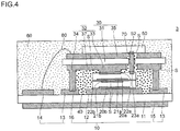
- a semiconductor module 3 of the embodiment 3 has substantially the same configuration as the semiconductor module 1 of the embodiment 1. However, the semiconductor module 3 of the embodiment 3 differs from the semiconductor module 1 of the embodiment 1 with respect to the configuration of a power device part. That is, in the semiconductor module 3 of the embodiment 3, as shown in Fig. 4 , the power device part has the structure where two semiconductor elements 20a, 20b are stacked.
- the power device part has the structure where the semiconductor element 20a having three terminals are stacked on the semiconductor element 20b having two terminals.
- a first electrode 21a formed on one surface (lower surface) of the semiconductor element 20a is electrically connected to a second electrode 22b of the semiconductor element 20b
- a second electrode 22a formed on the other surface (upper surface) of the semiconductor element 20a is electrically connected to a bonding portion 33a having three terminals
- a gate electrode 23a is electrically connected to a control signal output terminal 52 of a control IC 50 through a connector 70.
- a first electrode 21b formed on one surface (lower surface) of the semiconductor element 20b is electrically connected to a first conductor layer 12, and a second electrode 22b formed on the other surface (upper surface) of the semiconductor element 20b is electrically connected to the first electrode 21a of the semiconductor element 20a having three terminals.
- the semiconductor module 3 of the embodiment 3 differs from the semiconductor module 1 of the embodiment 1 with respect to the configuration of the power device part.
- a first substrate 10 the power device part (semiconductor elements 20a, 20b), a second substrate 30 and the control IC 50 are stacked in this order.
- the semiconductor module includes the control IC 50 which controls the power device part, it is unnecessary to secure a region where the control IC 50 is mounted on one surface side of a first insulating substrate 11 and hence, it is possible to narrow an area occupied by parts compared to the case where the control IC 50 is mounted in a juxtaposed manner with the power device part on one surface side of the first insulating substrate 11.
- the semiconductor module 3 of the embodiment 3 it is possible to provide a semiconductor module which satisfies a demand for miniaturization of a product.
- the power device part has the structure where two semiconductor elements 20a, 20b are stacked. Accordingly, it is possible to narrow an area occupied by parts compared to the case where two semiconductor elements 20a, 20b are mounted in a juxtaposed manner on one surface side of the first insulating substrate 11. As a result, it is possible to provide a semiconductor module which satisfies a demand for miniaturization of a product at a high level.
- the semiconductor module 3 of the embodiment 3 has substantially the same configuration as the semiconductor module 1 of the embodiment 1 with respect to points except for the configuration of the power device part. Accordingly, out of the advantageous effects which the semiconductor module 1 of the embodiment 1 acquires, the semiconductor module 3 of the embodiment 3 can acquire advantageous effects brought about by the substantially same configuration.
- a semiconductor module 4 of the embodiment 4 has substantially the same configuration as the semiconductor module 3 of the embodiment 3. However, the semiconductor module 4 of the embodiment 4 differs from the semiconductor module 3 of the embodiment 3 with respect to a point where the semiconductor module 4 includes a second connecting member. That is, in the semiconductor module 4 of the embodiment 4, as shown in Fig. 5 , the semiconductor module 4 includes the second connecting member 82 having one end thereof sandwiched between two semiconductor elements 20a, 20b and the other end thereof electrically connected to a fifth conductor layer 17 described later.
- the second connecting member 82 is formed by blanking or bending a metal plate (for example, aluminum plate). One end of the second connecting member 82 is formed one size larger than two semiconductor elements 20a, 20b as viewed in a plan view, an upper side (second substrate side) at one end of the second connecting member 82 is bonded to a first electrode 21a of the semiconductor element 20a by a bonding material (solder), and a lower side (first substrate side) at one end of the second connecting member 82 is bonded to a second electrode 22b of the semiconductor element 20b by a bonding material (solder).
- a bonding material for example, aluminum plate
- a first substrate 10 further includes a fifth conductor layer 17 disposed at a position spaced apart from both of a first conductor layer 12 and an external-connection-use conductor layer 14.
- the fifth conductor layer 17 is connected with an external circuit (not shown in the drawing), since a portion of the fifth conductor layer 17 is not covered by an outer resin portion 60 or the fifth conductor layer 17 is connected with a terminal for external connection (not shown in the drawing).
- the surrounding wall portion 34b is formed only at a predetermined portion of the position which surrounds a bonding portion 33b as viewed in a plan view (a position which surrounds 3/4 of the whole circumference of the bonding portion 33) (see Fig. 5(b) ). That is, the surrounding wall portion 34b has a U shape as viewed in a plan view.
- the second connecting member 82 is formed such that the second connecting member 82 passes through "a space sandwiched by a first insulating substrate 11 and a second insulating substrate 31b at the position which surrounds the bonding portion 33b as viewed in a plan view and where the surrounding wall portion 34b is not formed".
- the semiconductor module 4 of the embodiment 4 differs from the semiconductor module 3 of the embodiment 3 with respect to a point where the semiconductor module 4 includes the second connecting member.
- the first substrate 10, the power device part (semiconductor elements 20a, 20b), a second substrate 30b and a control IC 50 are stacked in this order.
- the semiconductor module includes the control IC 50 which controls the power device part, it is unnecessary to secure a region where the control IC 50 is mounted on one surface side of the first insulating substrate 11 and hence, it is possible to narrow an area occupied by parts compared to the case where the control IC 50 is mounted in a juxtaposed manner with the power device part on one surface side of the first insulating substrate 11.
- the semiconductor module 4 of the embodiment 4 it is possible to provide a semiconductor module which satisfies a demand for miniaturization of a product.
- the semiconductor module 4 includes the second connecting member 82 having one end thereof sandwiched between two semiconductor elements 20a, 20b and the other end thereof electrically connected to the fifth conductor layer 17. Accordingly, it is possible to provide the semiconductor module having the higher degree of freedom in design.
- the semiconductor module 4 of the embodiment 4 has substantially the same configuration as the semiconductor module 3 of the embodiment 3 with respect to points except for the point where the semiconductor module 4 includes the second connecting member. Accordingly, out of the advantageous effects which the semiconductor module 3 of the embodiment 3 acquires, the semiconductor module 4 of the embodiment 4 can acquire advantageous effects brought about by the substantially same configuration.
- a semiconductor module 5 of the embodiment 5 has substantially the same configuration as the semiconductor module 3 of the embodiment 3. However, the semiconductor module 5 of the embodiment 5 differs from the semiconductor module 3 of the embodiment 3 with respect to the configuration of a power device part. That is, in the semiconductor module 5 of the embodiment 5, as shown in Fig. 6 , both of two semiconductor elements 20a, 20c (assuming the semiconductor element on a second substrate side as the semiconductor element 20a and the semiconductor element on a first substrate side as the semiconductor element 20c) have a first electrode 21a, 21c on one surface and a second electrode 22a, 22c and two gate electrodes 23a, 23c on the other surface.
- Each of the two semiconductor elements 20a, 20c is stacked such that the whole semiconductor element is positioned inside a region defined by a surrounding wall portion 34 as viewed in a plan view.
- a second insulating substrate 31 has holes which respectively correspond to the gate electrodes 23a, 23c of two semiconductor elements 20a, 20c, and connectors 70a, 70c are disposed in the inside of the respective holes.
- the semiconductor module 5 of the embodiment 5 differs from the semiconductor module 3 of the embodiment 3 with respect to the configuration of the power device part.
- a first substrate 10 the power device part (semiconductor elements 20a, 20c), a second substrate 30 and a control IC 50 are stacked in this order.
- the semiconductor module includes the control IC 50 which controls the power device part, it is unnecessary to secure a region where the control IC 50 is mounted on one surface side of the first insulating substrate 11 and hence, it is possible to narrow an area occupied by parts compared to the case where the control IC 50 is mounted in a juxtaposed manner with the power device part on one surface side of the first insulating substrate 11.
- the semiconductor module 5 of the embodiment 5 it is possible to provide a semiconductor module which satisfies a demand for miniaturization of a product.
- each of the two semiconductor elements 20a, 20c is stacked such that the whole semiconductor element is positioned inside a region defined by the surrounding wall portion 34 as viewed in a plan view. Accordingly, it is possible to completely shield the two semiconductor elements 20a, 20c by the surrounding wall portion 34 from the outside. As a result, it is possible to prevent with certainty the occurrence of a phenomenon that oscillations are generated or an erroneous operation occurs in the two semiconductor elements 20a, 20c due to noises from the outside.
- the semiconductor module 5 of the embodiment 5 has substantially the same configuration as the semiconductor module 3 of the embodiment 3 with respect to points except for the configuration of the power device part. Accordingly, out of the advantageous effects which the semiconductor module 3 of the embodiment 3 acquires, the semiconductor module 5 of the embodiment 5 can acquire advantageous effects brought about by the substantially same configuration.
- a semiconductor module 6 of the embodiment 6 has substantially the same configuration as the semiconductor module 5 of the embodiment 5. However, the semiconductor module 6 of the embodiment 6 differs from the semiconductor module 5 of the embodiment 5 with respect to the configuration of a power device part. That is, in the semiconductor module 6 of the embodiment 6, as shown in Fig. 7 , one of the two semiconductor elements (semiconductor element 20c on a lower side) is stacked such that a gate electrode 23c of a semiconductor element 20c is positioned outside a region defined by a surrounding wall portion 34c as viewed in a plan view.
- the semiconductor module 6 of the embodiment 6 further includes a second connecting member 82 having one end thereof sandwiched between two semiconductor elements 20a, 20c and the other end thereof electrically connected to a fifth conductor layer 17.
- One end of the second connecting member 82 is formed one size larger than semiconductor elements 20a, 20c as viewed in a plan view, an upper side (second substrate side) at one end of the second connecting member 82 is bonded to a first electrode 21a of the semiconductor element 20a by a bonding material (solder), and a lower side (first substrate side) at one end of the second connecting member 82 is bonded to a second electrode 22c of the semiconductor element 20c by a bonding material (solder).
- the surrounding wall portion 34c is formed only at a predetermined portion of the position which surrounds a bonding portion 33c as viewed in a plan view (a position which surrounds a half of the whole circumference of the bonding portion 33 as viewed in a plan view) (see Fig. 7(b) ). That is, the surrounding wall portion 34c has an L shape as viewed in a plan view.
- the gate electrode 23c of the semiconductor element 20c (on a lower side) is electrically connected with a control signal output terminal 52b of a control IC 50b disposed at a position spaced apart from the surrounding wall portion 34c through a wire 80.
- the gate electrode 23c be away from an outer periphery of a region defined by the surrounding wall portion 34c as viewed in a plan view three times as large as a width of the gate electrode 23c in the predetermined direction.
- the semiconductor module 6 of the embodiment 6 differs from the semiconductor module 5 of the embodiment 5 with respect to the configuration of the power device part.
- a first substrate 10 the power device part (semiconductor elements 20a, 20c), a second substrate 30c and the control IC 50b are stacked in this order.
- the semiconductor module includes the control IC 50a which controls the power device part, it is unnecessary to secure a region where the control IC 50a is mounted on one surface side of a first insulating substrate 11 and hence, it is possible to narrow an area occupied by parts compared to the case where the control IC 50a is mounted in a juxtaposed manner with the power device part on one surface side of the first insulating substrate 11.
- the semiconductor module 6 of the embodiment 6 it is possible to provide a semiconductor module which satisfies a demand for miniaturization of a product.
- the gate electrode 23c of the semiconductor element 20c is stacked such that the gate electrode 23c is positioned outside a region defined by the surrounding wall portion 34c as viewed in a plan view. Accordingly, even in the case where the second substrate 30c is provided over the most portion of the power device part, the gate electrode 23c of the power device part and the control signal output terminal 52b of the control IC 50b can be connected with each other by the wire 80 having a small diameter. As a result, as the semiconductor module 6 of the embodiment 6, it is possible to provide a semiconductor module capable of controlling the power device part (the semiconductor element 20c on a lower side of the power device part) by the control IC 50b.
- the semiconductor module 6 of the embodiment 6 has substantially the same configuration as the semiconductor module 5 of the embodiment 5 with respect to points except for the configuration of the power device part. Accordingly, out of the advantageous effects which the semiconductor module 5 of the embodiment 5 acquires, the semiconductor module 6 of the embodiment 6 can acquire advantageous effects brought about by the substantially same configuration.
- a semiconductor module 7 of the embodiment 7 has substantially the same configuration as the semiconductor module 1 of the embodiment 1. However, the semiconductor module 7 of the embodiment 7 differs from the semiconductor module 1 of the embodiment 1 with respect to the configuration of a surrounding wall portion. That is, in the semiconductor module 7 of the embodiment 7, as shown in Fig. 8 , the surrounding wall portion 34d is formed in a state where the surrounding wall portion 34d is spaced apart from a bonding portion 33d.
- the first substrate 10 further includes a fourth conductor layer 13 which is bonded to the surrounding wall portion 34d at a position spaced apart from a first conductor layer 12 on one-surface side of a first insulating substrate 11, and a groove portion 16 which engages with the surrounding wall portion 34d is formed on the fourth conductor layer 13.
- the semiconductor module 7 of the embodiment 7 differs from the semiconductor module 1 of the embodiment 1 with respect to the configuration of the surrounding wall portion.
- the semiconductor module 1 of the embodiment 1 the first substrate 10, the power device part (semiconductor element 20), a second substrate 30d and a control IC 50 are stacked in this order. Accordingly, even in the case where the semiconductor module includes the control IC 50 which controls the power device part, it is unnecessary to secure a region where the control IC 50 is mounted on one surface side of the first insulating substrate 11 and hence, it is possible to narrow an area occupied by parts compared to the case where the control IC 50 is mounted in a juxtaposed manner with the power device part on one surface side of the first insulating substrate 11. As a result, as the semiconductor module 7 of the embodiment 7, it is possible to provide a semiconductor module which satisfies a demand for miniaturization of a product.
- the surrounding wall portion 34d is formed in a state where the surrounding wall portion 34d is spaced apart from the bonding portion 33d. Accordingly, it is possible to prevent the bonding portion 33d from being short-circuited with the other conductor layers or other semiconductor elements through the surrounding wall portion 34d and hence, it is possible to provide the semiconductor module which is minimally broken.
- the semiconductor module 7 of the embodiment 7 has substantially the same configuration as the semiconductor module 1 of the embodiment 1 with respect to points except for the configuration of the surrounding wall portion. Accordingly, out of the advantageous effects which the semiconductor module 1 of the embodiment 1 acquires, the semiconductor module 7 of the embodiment 7 can acquire advantageous effects brought about by the substantially same configuration.
Landscapes
- Cooling Or The Like Of Semiconductors Or Solid State Devices (AREA)
- Engineering & Computer Science (AREA)
- Chemical & Material Sciences (AREA)
- Ceramic Engineering (AREA)
- Physics & Mathematics (AREA)
- Health & Medical Sciences (AREA)
- Electromagnetism (AREA)
- Toxicology (AREA)
- Structures Or Materials For Encapsulating Or Coating Semiconductor Devices Or Solid State Devices (AREA)
- Inverter Devices (AREA)
- Microelectronics & Electronic Packaging (AREA)
- Production Of Multi-Layered Print Wiring Board (AREA)
Abstract
Description
- The present invention relates to a semiconductor module.
- Conventionally, there has been known a semiconductor module having a substrate and a semiconductor element (see
patent literature 1, for example). - As shown in
Fig. 9 , theconventional semiconductor module 8 includes: asubstrate 810 having aninsulating substrate 811, aconductor layer 812 formed on one surface of theinsulating substrate 811 andother conductor layers conductor layer 812; a device part (semiconductor element) 820 having afirst electrode 821 on one surface (a lower surface inFig. 9 ) and twosecond electrodes Fig. 9 ) and making thefirst electrode 821 and theconductor layer 812 bonded to each other; awall portion 816 formed along an outer periphery of theinsulating substrate 811; aresin portion 860 formed in a state where a resin is disposed in a recessed space which is defined by theinsulating substrate 811 and thewall portion 816; a resin-madelid portion 862 disposed on an upper surface of theresin portion 860; andterminals terminals other conductor layers terminals resin portion 860 and thelid portion 862 from the one-side ends. - Out of two
second electrodes semiconductor element 820, onesecond electrode 822 is electrically connected to theterminal 874 through awire 870 and theother conductor layer 813, and the othersecond electrode 823 is electrically connected to theterminal 876 through awire 872. - The
conventional semiconductor module 8 has theresin portion 860 which is formed by disposing a resin in the recessed space defined by thesubstrate 810 and thewall portion 816 thus providing a semiconductor module having impact resistance. - Recently, in the technical field of semiconductor modules, there has been a demand for a semiconductor module where the structure for resin sealing can be easily formed.
- Under such circumstances, inventors of the present invention have come up with a semiconductor module where the structure for resin sealing can be easily formed, and already filed international patent application
PCT/JP2015/051655 - As shown in
Fig. 10 , asemiconductor module 9 relating to the prior patent application includes:
afirst substrate 910 having a firstinsulating substrate 911 and afirst conductor layer 912 which is formed on at least one surface of the firstinsulating substrate 911; a device part (semiconductor element) 920 having afirst electrode 921 on one surface thereof and asecond electrode 922 on the other surface thereof and having thefirst electrode 921 bonded to thefirst conductor layer 912; asecond substrate 930 having a secondinsulating substrate 931 and asecond conductor layer 932 formed on at least one surface of the secondinsulating substrate 931, wherein thesecond conductor layer 932 has abonding portion 933 bonded to thesecond electrode 922 and a surroundingwall portion 934 formed at a position which surrounds thebonding portion 933 as viewed in a plan view in a state where an upper end surface of the surroundingwall portion 934 projects from a bonding surface between thebonding portion 933 and thesecond electrode 922, and thesecond substrate 930 is brought into contact with thefirst substrate 910 by way of the surroundingwall portion 934; and aresin portion 940 made of a resin and disposed in a space defined by the surroundingwall portion 934 and sandwiched between the firstinsulating substrate 911 and the secondinsulating substrate 931. - In the
semiconductor module 9 according to the prior patent application, thedrive part 920 is disposed such that thewhole device part 920 is positioned inside a region defined by the surroundingwall portion 934 as viewed in a plan view. - In the
semiconductor module 9 according to the prior patent application, thesecond conductor layer 932 includes the surroundingwall portion 934 formed at the position which surrounds thebonding portion 933 as viewed in a plan view in a state where an upper end surface of the surroundingwall portion 934 projects from the bonding surface between thebonding portion 933 and thesecond electrode 922. Accordingly, it is unnecessary to additionally prepare a member for forming the structure for resin sealing (for example, thewall portion 816 in the conventional semiconductor module 8) and hence, the structure for resin sealing can be formed easily. - Further, in the
semiconductor module 9 according to the prior patent application, thesecond electrode 922 of thedevice part 920 is bonded to thesecond conductor layer 932 formed on the one surface of the secondinsulating substrate 931. With such a configuration, in addition to the radiation of heat generated by thedevice part 920 to the outside through thefirst conductor layer 912 and the firstinsulating substrate 911, such heat can be radiated to the outside through thesecond conductor layer 932 and the secondinsulating substrate 931. Accordingly, as thesemiconductor module 9 according to the prior patent application, it is possible to provide a semiconductor module having higher heat radiation property than conventional semiconductor modules. - PTL 1:
JP-A-2006-134990 - Recently, in a technical field of semiconductor modules, there has been requested a semiconductor module which satisfies a demand for miniaturization of a product. However, in such a semiconductor module, in the case where a power device part (power semiconductor element) having a gate electrode is used as a device part, and a control IC which controls the power device part is mounted on one surface side of a first insulating substrate, it is necessary to secure a region where the control IC is mounted on one surface side of the first insulating substrate and hence, an area occupied by parts is expanded. Accordingly, there arises a drawback that a semiconductor module which satisfies a demand for miniaturization of a product cannot be provided.
- The present invention has been made to overcome the above-mentioned drawbacks, and it is an object of the present invention to provide a semiconductor module which satisfies a demand for miniaturization of a product even in the case where a semiconductor module includes a control IC which controls a power device part.
-
- [1] A semiconductor module of the present invention includes: a first substrate having a first insulating substrate and a first conductor layer which is formed on one-surface side of the first insulating substrate; a power device part having a first electrode on one surface thereof and a second electrode and a gate electrode on the other surface thereof, and having the first electrode electrically connected to the first conductor layer; a second substrate having a second insulating substrate, a second conductor layer formed on one-surface side of the second insulating substrate and a third conductor layer formed on the other surface of the second insulating substrate, wherein a hole is formed in the second insulating substrate at a position corresponding to a position of the gate electrode, the second conductor layer has a bonding portion bonded to the second electrode and a surrounding wall portion formed at a position which surrounds the bonding portion as viewed in a plan view in a state where an upper end surface of the surrounding wall portion projects from a bonding surface between the second electrode and the bonding portion, and the second substrate is brought into contact with the first substrate by way of the surrounding wall portion; an inner resin portion made of a resin and disposed in a space defined by the surrounding wall portion and sandwiched between the first insulating substrate and the second insulating substrate; a control IC disposed on the third conductor layer; and an outer resin portion made of a resin and disposed on one surface side of the first substrate so as to cover the second substrate and the control IC, wherein the first substrate, the power device part, the second substrate and the control IC are stacked in this order, wherein a connecting member is disposed in the inside of the hole formed in the second insulating substrate, and the gate electrode is electrically connected to a control signal output terminal of the control IC through the connecting member.
In this specification, "a surrounding wall portion formed at a position which surrounds the bonding portion" includes not only the case where the surrounding wall portion is formed at a position which surrounds the whole circumference of the bonding portion as viewed in a plan view but also the case where the surrounding wall portion is formed only at a predetermined portion of the position which surrounds the bonding portion. - [2] In the semiconductor module of the present invention, it is preferable that the surrounding wall portion be formed at a position which surrounds the whole circumference of the bonding portion as viewed in a plan view.
- [3] In the semiconductor module of the present invention, it is preferable that the surrounding wall portion be formed only at a predetermined portion of a position which surrounds the bonding portion as viewed in a plan view.
- [4] In the semiconductor module of the present invention, it is preferable that the surrounding wall portion be formed continuously with the bonding portion, the first substrate further have a fourth conductor layer which is bonded to the surrounding wall portion at a position spaced apart from the first conductor layer on one-surface side of the first insulating substrate, and the fourth conductor layer be electrically connected to the second electrode through the surrounding wall portion and the bonding portion.
In this specification, "the surrounding wall portion is formed continuously with the bonding portion" includes not only the case where the surrounding wall portion is disposed adjacently to the bonding portion but also the case where a member which differs from the surrounding wall portion and the bonding portion is sandwiched between the surrounding wall portion and the bonding portion. - [5] In the semiconductor module of the present invention, it is preferable that a groove portion which engages with the surrounding wall portion be formed on the fourth conductor layer.
- [6] In the semiconductor module of the present invention, it is preferable that the surrounding wall portion be formed in a state where the surrounding wall portion is spaced apart from the bonding portion.
- [7] In the semiconductor module of the present invention, it is preferable that the first substrate further have a fourth conductor layer which is bonded to the surrounding wall portion at a position spaced apart from the first conductor layer on one-surface side of the first insulating substrate, and a groove portion which engages with the surrounding wall portion be formed on the fourth conductor layer.
- [8] In the semiconductor module of the present invention, it is preferable that the power device part be formed of one semiconductor element, and the one semiconductor element have a first electrode on one surface thereof and have a second electrode and a gate electrode on the other surface thereof.
- [9] In the semiconductor module of the present invention, it is preferable that the power device part have the structure where a plurality of semiconductor elements are stacked, and at least one semiconductor element among the plurality of semiconductor elements have a first electrode on one surface thereof and have a second electrode and a gate electrode on the other surface thereof.
In this specification, when two or more semiconductor elements respectively have the gate electrode, and the semiconductor elements are stacked in a state where the respective gate electrodes are displaced from each other such that the respective gate electrodes can be electrically connected to the connecting member. - [10] In the semiconductor module of the present invention, it is preferable that the power device part have the structure where a plurality of semiconductor elements are stacked, the first substrate further have a fifth conductor layer disposed at a position spaced apart from the first conductor layer, and the semiconductor module further have a second connecting member which has one end thereof sandwiched between two semiconductor elements among the plurality of semiconductor elements and has the other end thereof electrically connected to the fifth conductor layer.
- [11] In the semiconductor module of the present invention, it is preferable that the power device part have the structure where a plurality of semiconductor elements are stacked, each of at least two semiconductor elements among the plurality of semiconductor elements have a first electrode on one surface thereof and have a second electrode and a gate electrode on the other surface thereof, and each of the at least two semiconductor elements be stacked such that the whole semiconductor element is positioned inside a region defined by the surrounding wall portion as viewed in a plan view.
- [12] In the semiconductor module of the present invention, it is preferable that the power device part have the structure where a plurality of semiconductor elements are stacked, each of at least two semiconductor elements among the plurality of semiconductor elements have a first electrode on one surface thereof and have a second electrode and a gate electrode on the other surface thereof, and at least one of the at least two semiconductor elements be stacked such that the gate electrode of the semiconductor element is positioned outside a region defined by the surrounding wall portion as viewed in a plan view.
- [13] In the semiconductor module of the present invention, it is preferable that the bonding portion and the surrounding wall portion be formed of one copper layer.
- According to the semiconductor module of the present invention, the first substrate, the power device part, the second substrate and the control IC are stacked in this order. Accordingly, even in the case where the semiconductor module includes the control IC which controls the power device part, it is unnecessary to secure a region where the control IC is mounted on one surface side of the first insulating substrate and hence, it is possible to narrow an area occupied by parts compared to the case where the control IC is mounted in a juxtaposed manner with the power device part on one surface side of the first insulating substrate. As a result, as the semiconductor module of the present invention, it is possible to provide a semiconductor module which satisfies a demand for miniaturization of a product.
- Further, according to the semiconductor module of the present invention, a hole is formed in the second insulating substrate at a position corresponding to the position of the gate electrode, a connecting member is disposed in the inside of the hole formed in the second insulating substrate, and the gate electrode is electrically connected to a control signal output terminal of the control IC through the connecting member. Accordingly, even when the control IC is disposed on the third conductor layer, it is possible to control the power device part by the control IC without being obstructed by the second insulating substrate.
- Further, according to the semiconductor module of the present invention, the connecting member is disposed in the inside of the hole formed in the second insulating substrate, and the gate electrode is electrically connected to the control signal output terminal of the control IC through the connecting member. Accordingly, a length of a line (a length of the connecting member) between the gate electrode of the power device part and the control signal output terminal of the control IC can be shortened and hence, the semiconductor module is minimally affected by noise from the outside.
- Further, according to the semiconductor module of the present invention, the second conductor layer has the surrounding wall portion which is formed at the position which surrounds the bonding portion as viewed in a plan view. Accordingly, even in the case where the inner resin portion ignites due to the generation of heat which occurs as a result of applying an excessive load to the power device part, the surrounding wall portion plays a role of a fire wall so that spreading of fire to the surrounding can be prevented.
- Still further, according to the semiconductor module of the present invention, the second conductor layer has the surrounding wall portion which is formed at the position which surrounds the bonding portion as viewed in a plan view. Accordingly, it is possible to shield the power device part from the outside by the surrounding wall portion and hence, it is possible to prevent the occurrence of a phenomenon that oscillations are generated or an erroneous operation occurs in the power device part due to noises from the outside of the power device part. As a result, it is possible to provide a semiconductor module where drawbacks caused by oscillations or an erroneous operation can be minimized as the semiconductor module of the present invention.
-
-
Fig. 1(a) and Fig. 1(b) are views showing asemiconductor module 1 of anembodiment 1, whereinFig. 1(a) is a cross-sectional view of thesemiconductor module 1, andFig. 1(b) is a planer cross-sectional view of thesemiconductor module 1 taken along a line A-A inFig. 1(a) . -
Fig. 2 (a) and Fig. 2(b) are views for describing asecond substrate 30, whereinFig. 2(a) is a plan view of thesecond substrate 30, andFig. 2(b) is a cross-sectional view of thesemiconductor module 2 taken along a line B-B inFig. 2(a) . -
Fig. 3(a) and Fig. 3(b) are views showing asemiconductor module 2 according to anembodiment 2, whereinFig. 3(a) is a cross-sectional view of thesemiconductor module 2, andFig. 3(b) is a planer cross-sectional view of thesemiconductor module 2 taken along a line C-C inFig. 3(a) . -
Fig. 4 is a cross-sectional view showing asemiconductor module 3 according to anembodiment 3. -
Fig. 5 (a) and Fig. 5(b) are views showing asemiconductor module 4 according to anembodiment 4, whereinFig. 5(a) is a cross-sectional view of thesemiconductor module 4, andFig. 5(b) is a planar cross-sectional view of thesemiconductor module 4 taken along a line D-D inFig. 5(a) . -
Fig. 6(a) and Fig. 6(b) are views showing asemiconductor module 5 according to anembodiment 5, whereinFig. 6(a) is a cross-sectional view of thesemiconductor module 5, andFig. 6(b) is a planar cross-sectional view of thesemiconductor module 5 taken along a line E-E inFig. 6(a) . -
Fig. 7 (a) and Fig. 7(b) are views showing asemiconductor module 6 according to anembodiment 6, whereinFig. 7(a) is a cross-sectional view of thesemiconductor module 6, andFig. 7(b) is a planar cross-sectional view of thesemiconductor module 6 taken along a line F-F inFig. 7(a) . -
Fig. 8 is a cross-sectional view showing asemiconductor module 7 according to anembodiment 7. -
Fig. 9 is a cross-sectional view showing aconventional semiconductor module 8, whereinsymbol 815 indicates a heat radiation conductor layer of asubstrate 810. -
Fig. 10 is a cross-sectional view showing asemiconductor module 9 according to a prior patent application. In the drawing,symbol 913 indicates a third conductor layer,symbol 915 indicates a heat radiation conductor layer of afirst substrate 910,symbol 916 indicates a groove portion,symbol 935 indicates a heat radiation conductor layer of asecond substrate 930,symbol 937 indicates a flat portion, and symbol S indicates a solder. - Hereinafter, a semiconductor module of the present invention is described in conjunction with an embodiment shown in drawings.
- As shown in
Fig. 1 , asemiconductor module 1 of theembodiment 1 includes: afirst substrate 10; a power device part; asecond substrate 30; aninner resin portion 40; acontrol IC 50; anouter resin portion 60; and a connector (connecting member) 70. Thefirst substrate 10, the power device part, thesecond substrate 30 and thecontrol IC 50 are stacked in this order. - The
first substrate 10 is a mounting substrate which has: a first insulatingsubstrate 11; afirst conductor layer 12 formed on one-surface side of the first insulatingsubstrate 11; afourth conductor layer 13 bonded to a surroundingwall portion 34 described later at a position spaced apart from thefirst conductor layer 12; an external-connection-use conductor layer 14 disposed at a position spaced apart from thefirst conductor layer 12 and thefourth conductor layer 13; and a heatradiation conductor layer 15 formed on the other surface of the first insulatingsubstrate 11. - In the
first substrate 10, the first insulatingsubstrate 11 is made of ceramics (for example, alumina), while thefirst conductor layer 12, thefourth conductor layer 13, the external-connection-use conductor layer 14 and the heatradiation conductor layer 15 are made of metal (for example, copper). Thefirst substrate 10 is a DCB substrate (direct copper bonding substrate) where the first insulatingsubstrate 11 and the respective conductor layers are bonded to each other by eutectic bonding. With such a configuration, it is possible to provide the semiconductor module having high heat radiation property. - A
groove portion 16 which engages with a surroundingwall portion 34 described later is formed on thefourth conductor layer 13. Thegroove portion 16 is formed by etching thefourth conductor layer 13. The external-connection-use conductor layer 14 is connected with an external circuit (not shown in the drawing), since a portion of the external-connection-use conductor layer 14 is not covered by anouter resin portion 60 or the external-connection-use conductor layer 14 is connected with a terminal for external connection (not shown in the drawing). The external-connection-use conductor layer 14 is electrically connected with an input terminal (or a control signal output terminal) of thecontrol IC 50 through athird conductor layer 35 and awire 80 described later. - The power device part is formed of one
semiconductor element 20. Afirst electrode 21 is formed on one surface (a lower side inFig. 1 ) of thesemiconductor element 20, and asecond electrode 22 and agate electrode 23 are formed on the other surface (an upper side inFig. 1 ) of thesemiconductor element 20. The power device part is disposed such that thewhole semiconductor element 20 is positioned inside a region defined by the surroundingwall portion 34 as viewed in a plan view. Thesemiconductor element 20 is a semiconductor element having three terminals (for example, IGBT). - The
gate electrode 23 is electrically connected to a controlsignal output terminal 52 of thecontrol IC 50 through theconnector 70. Thefirst electrode 21 is electrically connected to thefirst conductor layer 12 by bonding by a bonding material S (for example, solder), and thesecond electrode 22 is electrically connected to abonding portion 33 of thesecond substrate 30 described later by bonding by the bonding material S (for example, solder). - As shown in
Fig. 1 andFig. 2 , thesecond substrate 30 has: a second insulatingsubstrate 31; asecond conductor layer 32 formed on one-surface side of the second insulatingsubstrate 31; and athird conductor layer 35 formed on the other surface of the second insulatingsubstrate 31. In thesecond substrate 30, the second insulatingsubstrate 31 is made of ceramics (for example, alumina) while thesecond conductor layer 32 and thethird conductor layer 35 are made of metal (for example copper). Thesecond substrate 30 is a DCB substrate where the second insulatingsubstrate 31 and the respective conductor layers are bonded to each other by eutectic bonding. - As shown in
Fig. 2 , ahole 36 is formed in the second insulating substrate 31 (and thesecond conductor layer 32 and the third conductor layer 35) at a position corresponding to the position of thegate electrode 23. - As shown in
Fig. 1 andFig. 2 , thesecond conductor layer 32 has: a bondingportion 33 which is bonded to thesecond electrode 22; a surroundingwall portion 34 which is formed at a position which surrounds thebonding portion 33 as viewed in a plan view in a state where an upper end surface of the surroundingwall portion 34 projects from a bonding surface between thesecond electrode 22 and thebonding portion 33; and aflat portion 37. Thesecond substrate 30 is brought into contact with thefirst substrate 10 with the surroundingwall portion 34 interposed therebetween. Thebonding portion 33 and the surroundingwall portion 34 are formed by etching one copper layer. With such a configuration, thebonding portion 33 and the surroundingwall portion 34 can be formed with high accuracy. - The surrounding
wall portion 34 is formed at a position which surrounds the whole circumference of thebonding portion 33 as viewed in a plan view (seeFig. 1(b) ). That is, the surroundingwall portion 34 has a "hollow square" shape as viewed in a plan view. - The surrounding
wall portion 34 is formed continuously with thebonding portion 33 by way of theflat portion 37 of thesecond conductor layer 32. The surroundingwall portion 34 engages with thegroove portion 16 formed on thefourth conductor layer 13 of thefirst substrate 10, and is bonded to thegroove portion 16 by a bonding material (for example, solder). With such a configuration, thesecond electrode 22 and thefourth conductor layer 13 are electrically connected with each other through thebonding portion 33 and the surroundingwall portion 34. - A length from a boundary surface between the second insulating
substrate 31 and thesecond conductor layer 32 to an upper end surface of the surroundingwall portion 34 is set to a value which falls within a range of from 0.2 to 1.0mm, for example. A thickness of thebonding portion 33 is set to a value which falls within a range of from 0.15 to 0.5mm, for example. - As shown in
Fig. 1 , theinner resin portion 40 is made of a resin disposed in "a space defined by the surroundingwall portion 34 and sandwiched between the first insulatingsubstrate 11 and the second insulatingsubstrate 31". As the resin which is used for forming theinner resin portion 40, a suitable resin (for example, an epoxy resin) can be used. - The
control IC 50 controls driving of the power device part by controlling turning on or off of thegate electrode 23 of the power device part. Thecontrol IC 50 is disposed on thethird conductor layer 35. Thecontrol IC 50 has a predetermined controlsignal output terminal 52, and the controlsignal output terminal 52 and thegate electrode 23 are electrically connected with each other through theconnector 70 described later. - The
outer resin portion 60 is made of a resin, and is disposed on one surface side of thefirst substrate 10 so as to cover at least thesecond substrate 30 and thecontrol IC 50. Although a resin equal to a resin for forming theinner resin portion 40 is used as the resin for forming theouter resin portion 60, a resin which differs from the resin for forming theinner resin portion 40 can be also used. - The connector (connecting member) 70 is disposed in the inside of the
hole 36 formed in the second insulatingsubstrate 31. Theconnector 70 has an elongated columnar shape. One end of theconnector 70 is electrically connected to thegate electrode 23 of the power device part, and the other end of theconnector 70 is electrically connected to the controlsignal output terminal 52 of thecontrol IC 50. Theconnector 70 is formed by blanking or bending a metal plate. As a material of the metal plate, a suitable material (for example, aluminum) can be used. - According to the
semiconductor module 1 of theembodiment 1, thefirst substrate 10, the power device part (semiconductor element 20), thesecond substrate 30 and thecontrol IC 50 are stacked in this order. Accordingly, even in the case where thesemiconductor module 1 includes thecontrol IC 50 which controls the power device part, it is unnecessary to secure a region where thecontrol IC 50 is mounted on one surface side of the first insulatingsubstrate 11 and hence, it is possible to narrow an area occupied by parts compared to the case where thecontrol IC 50 is mounted in a juxtaposed manner with the power device part on one surface side of the first insulatingsubstrate 11. As a result, as thesemiconductor module 1 of theembodiment 1, it is possible to provide a semiconductor module which satisfies a demand for miniaturization of a product. - Further, according to the
semiconductor module 1 of theembodiment 1, thehole 36 is formed in the second insulatingsubstrate 31 at a position corresponding to the position of thegate electrode 23, aconnector 70 is disposed in the inside of thehole 36 formed in the second insulatingsubstrate 31, and thegate electrode 23 is electrically connected to a controlsignal output terminal 52 of thecontrol IC 50 through theconnector 70. Accordingly, even when thecontrol IC 50 is disposed on thethird conductor layer 35, it is possible to control the power device part by thecontrol IC 50 without being obstructed by the second insulatingsubstrate 31. - Further, according to the
semiconductor module 1 of theembodiment 1, theconnector 70 is disposed in the inside of thehole 36 formed in the second insulatingsubstrate 31, and thegate electrode 23 is electrically connected to the controlsignal output terminal 52 of thecontrol IC 50 through theconnector 70. Accordingly, a length of a line (a length of the connector 70) between thegate electrode 23 of the power device part and the controlsignal output terminal 52 of thecontrol IC 50 can be shortened and hence, thesemiconductor module 1 is minimally affected by noises from the outside. - Further, according to the
semiconductor module 1 of theembodiment 1, thesecond conductor layer 32 has the surroundingwall portion 34 which is formed at the position which surrounds thebonding portion 33 as viewed in a plan view. Accordingly, in the case where theinner resin portion 40 ignites due to the generation of heat which occurs as a result of applying an excessive load to the power device part, the surroundingwall portion 34 plays a role of a fire wall so that spreading of fire to the surrounding can be prevented. - Still further, according to the
semiconductor module 1 of theembodiment 1, thesecond conductor layer 32 has the surroundingwall portion 34 which is formed at the position which surrounds thebonding portion 33 as viewed in a plan view. Accordingly, it is possible to shield the power device part from the outside by the surroundingwall portion 34 and hence, it is possible to prevent the occurrence of a phenomenon that oscillations are generated or an erroneous operation occurs in the power device part due to noises from the outside of the power device part. As a result, it is possible to provide a semiconductor module where drawbacks caused by oscillations or an erroneous operation can be minimized as thesemiconductor module 1 of theembodiment 1. - According to the
semiconductor module 1 of theembodiment 1, the surroundingwall portion 34 is formed at a position which surrounds the whole circumference of thebonding portion 33 as viewed in a plan view. Accordingly, in the case where theinner resin portion 40 ignites due to the generation of heat which occurs as a result of applying an excessive load to the power device part, the surroundingwall portion 34 completely surrounds theinner resin portion 40 so that spreading of fire to the surrounding can be prevented with certainty. Further, it is possible to completely shield the power device part from the outside by the surroundingwall portion 34 and hence, it is possible to prevent with certainty the occurrence of a phenomenon that oscillations are generated or an erroneous operation occurs in the power device part due to noises from the outside of the power device part. - In the
semiconductor module 1 of theembodiment 1, the surroundingwall portion 34 is formed continuously with thebonding portion 33, thefirst substrate 10 further includes afourth conductor layer 13 which is bonded to the surroundingwall portion 34 at a position spaced apart from thefirst conductor layer 12 on one-surface side of the second insulatingsubstrate 31, and thefourth conductor layer 13 is electrically connected to thesecond electrode 22 through the surroundingwall portion 34 and thebonding portion 33. - With such a configuration, the
second electrode 22 of the power device part can be electrically connected to the outside through thebonding portion 33, the surroundingwall portion 34 and thefourth conductor layer 13. All of thebonding portion 33, the surroundingwall portion 34 and thefourth conductor layer 13 have larger cross-sectional areas and lower resistances than the wire and hence, when a large electric current is supplied to the semiconductor module, drawbacks minimally occur and hence, it is possible to provide a semiconductor module having further reliability. - According to the
semiconductor module 1 of theembodiment 1, thesemiconductor module 1 has the above-mentioned configuration and hence, heat generated by the power device part can be radiated to the outside through thebonding portion 33, the surroundingwall portion 34 and thefourth conductor layer 13 whereby it is possible to provide a semiconductor module having further heat radiation property. - According to the
semiconductor module 1 of theembodiment 1, thegroove portion 16 which engages with the surroundingwall portion 34 is formed on thefourth conductor layer 13. Accordingly, in steps of manufacturing the semiconductor module, at the time of mounting thesecond substrate 30 on thefirst substrate 10, it is possible to easily position thesecond substrate 30 by fitting thesurrounding wall portion 34 of thesecond substrate 30 into thegroove portion 16 of thefourth conductor layer 13. - According to the
semiconductor module 1 of theembodiment 1, the power device part is formed of onesemiconductor element 20, and thesemiconductor element 20 has thefirst electrode 21 on one surface thereof and has thesecond electrode 22 and thegate electrode 23 on the other surface thereof. Accordingly, it is possible to provide a semiconductor module where a design of wiring can be performed easily. - According to the
semiconductor module 1 of theembodiment 1, thebonding portion 33 and the surroundingwall portion 34 are formed of one copper layer. Accordingly, in the manufacturing steps of the semiconductor module, even when thesemiconductor module 1 is introduced into a high temperature furnace for melting a bonding material (for example, solder), a length of the surroundingwall portion 34 minimally changes. Accordingly, a load applied to thesecond substrate 30 is dispersed to the surroundingwall portion 34 and hence, there is no possibility that the load applied to thesecond substrate 30 concentrates on the power device part. As a result, in the steps of manufacturing the semiconductor module, the power device part is minimally broken and hence, not only the semiconductor module can be manufactured at a high yield but also it is possible to prevent a change in thickness of a bonding material (for example, solder) even when the semiconductor module is introduced into a high temperature furnace for melting the bonding material and hence, it is possible to provide a highly reliable semiconductor module. - According to the
semiconductor module 1 of theembodiment 1, thebonding portion 33 and the surroundingwall portion 34 are formed of one copper layer. Accordingly, there is no possibility that the surroundingwall portion 34 is inclined. Accordingly, in the steps of manufacturing the semiconductor module, there is no possibility that thesecond substrate 30 is rotated in the θ direction as viewed in a plan view and hence, it is possible to accurately position thesecond substrate 30. - A
semiconductor module 2 of theembodiment 2 has substantially the same configuration as thesemiconductor module 1 of theembodiment 1. However, thesemiconductor module 2 of theembodiment 2 differs from thesemiconductor module 1 of theembodiment 1 with respect to the configuration of a surrounding wall portion. That is, in thesemiconductor module 2 of theembodiment 2, as shown inFig. 3 , the surroundingwall portion 34 is formed only at a predetermined portion of the position which surrounds abonding portion 33 as viewed in a plan view (the position which surrounds 3/4 of the whole circumference of the bonding portion 33) (seeFig. 3(b) ). That is, the surroundingwall portion 34 has a U shape as viewed in a plan view. - In this manner, the
semiconductor module 2 of theembodiment 2 differs from thesemiconductor module 1 of theembodiment 1 with respect to the configuration of the surrounding wall portion. However, in the same manner as thesemiconductor module 1 of theembodiment 1, afirst substrate 10, a power device part (semiconductor element 20), asecond substrate 30a and acontrol IC 50 are stacked in this order. Accordingly, even in the case where the semiconductor module includes thecontrol IC 50 which controls the power device part, it is unnecessary to secure a region where thecontrol IC 50 is mounted on one surface side of a first insulatingsubstrate 11 and hence, it is possible to narrow an area occupied by parts compared to the case where thecontrol IC 50 is mounted in a juxtaposed manner with the power device part on one surface side of the first insulatingsubstrate 11. As a result, as thesemiconductor module 2 of theembodiment 2, it is possible to provide a semiconductor module which satisfies a demand for miniaturization of a product. - According to the
semiconductor module 2 of theembodiment 2, the surroundingwall portion 34a is formed only at a predetermined portion of the position which surrounds thebonding portion 33 as viewed in a plan view. Accordingly, in forming theinner resin portion 40, a resin can be filled into a space defined by the surroundingwall portion 34 and sandwiched between a first insulatingsubstrate 11 and a second insulatingsubstrate 31 through "a space sandwiched by the first insulatingsubstrate 11 and the second insulatingsubstrate 31 at the portion of the position which surrounds abonding portion 33 as viewed in a plan view where the surroundingwall portion 34 is not formed". - The
semiconductor module 2 of theembodiment 2 has substantially the same configuration as thesemiconductor module 1 of theembodiment 1 with respect to points except for the configuration of the surrounding wall portion. Accordingly, out of the advantageous effects which thesemiconductor module 1 of theembodiment 1 acquires, thesemiconductor module 2 of theembodiment 2 can acquire advantageous effects brought about by the substantially same configuration. - A
semiconductor module 3 of theembodiment 3 has substantially the same configuration as thesemiconductor module 1 of theembodiment 1. However, thesemiconductor module 3 of theembodiment 3 differs from thesemiconductor module 1 of theembodiment 1 with respect to the configuration of a power device part. That is, in thesemiconductor module 3 of theembodiment 3, as shown inFig. 4 , the power device part has the structure where twosemiconductor elements - In the semiconductor module of the
embodiment 3, the power device part has the structure where thesemiconductor element 20a having three terminals are stacked on thesemiconductor element 20b having two terminals. - In the
semiconductor element 20a having three terminals, afirst electrode 21a formed on one surface (lower surface) of thesemiconductor element 20a is electrically connected to asecond electrode 22b of thesemiconductor element 20b, asecond electrode 22a formed on the other surface (upper surface) of thesemiconductor element 20a is electrically connected to abonding portion 33a having three terminals, and agate electrode 23a is electrically connected to a controlsignal output terminal 52 of acontrol IC 50 through aconnector 70. - In the
semiconductor element 20b having two terminals, afirst electrode 21b formed on one surface (lower surface) of thesemiconductor element 20b is electrically connected to afirst conductor layer 12, and asecond electrode 22b formed on the other surface (upper surface) of thesemiconductor element 20b is electrically connected to thefirst electrode 21a of thesemiconductor element 20a having three terminals. - In this manner, the
semiconductor module 3 of theembodiment 3 differs from thesemiconductor module 1 of theembodiment 1 with respect to the configuration of the power device part. However, in the same manner as thesemiconductor module 1 of theembodiment 1, afirst substrate 10, the power device part (semiconductor elements second substrate 30 and thecontrol IC 50 are stacked in this order. Accordingly, even in the case where the semiconductor module includes thecontrol IC 50 which controls the power device part, it is unnecessary to secure a region where thecontrol IC 50 is mounted on one surface side of a first insulatingsubstrate 11 and hence, it is possible to narrow an area occupied by parts compared to the case where thecontrol IC 50 is mounted in a juxtaposed manner with the power device part on one surface side of the first insulatingsubstrate 11. As a result, as thesemiconductor module 3 of theembodiment 3, it is possible to provide a semiconductor module which satisfies a demand for miniaturization of a product. - Still further, in the
semiconductor module 3 of theembodiment 3, the power device part has the structure where twosemiconductor elements semiconductor elements substrate 11. As a result, it is possible to provide a semiconductor module which satisfies a demand for miniaturization of a product at a high level. - The
semiconductor module 3 of theembodiment 3 has substantially the same configuration as thesemiconductor module 1 of theembodiment 1 with respect to points except for the configuration of the power device part. Accordingly, out of the advantageous effects which thesemiconductor module 1 of theembodiment 1 acquires, thesemiconductor module 3 of theembodiment 3 can acquire advantageous effects brought about by the substantially same configuration. - A
semiconductor module 4 of theembodiment 4 has substantially the same configuration as thesemiconductor module 3 of theembodiment 3. However, thesemiconductor module 4 of theembodiment 4 differs from thesemiconductor module 3 of theembodiment 3 with respect to a point where thesemiconductor module 4 includes a second connecting member. That is, in thesemiconductor module 4 of theembodiment 4, as shown inFig. 5 , thesemiconductor module 4 includes the second connectingmember 82 having one end thereof sandwiched between twosemiconductor elements fifth conductor layer 17 described later. - The second connecting
member 82 is formed by blanking or bending a metal plate (for example, aluminum plate). One end of the second connectingmember 82 is formed one size larger than twosemiconductor elements member 82 is bonded to afirst electrode 21a of thesemiconductor element 20a by a bonding material (solder), and a lower side (first substrate side) at one end of the second connectingmember 82 is bonded to asecond electrode 22b of thesemiconductor element 20b by a bonding material (solder). - A
first substrate 10 further includes afifth conductor layer 17 disposed at a position spaced apart from both of afirst conductor layer 12 and an external-connection-use conductor layer 14. Thefifth conductor layer 17 is connected with an external circuit (not shown in the drawing), since a portion of thefifth conductor layer 17 is not covered by anouter resin portion 60 or thefifth conductor layer 17 is connected with a terminal for external connection (not shown in the drawing). - The surrounding
wall portion 34b is formed only at a predetermined portion of the position which surrounds a bonding portion 33b as viewed in a plan view (a position which surrounds 3/4 of the whole circumference of the bonding portion 33) (seeFig. 5(b) ). That is, the surroundingwall portion 34b has a U shape as viewed in a plan view. The second connectingmember 82 is formed such that the second connectingmember 82 passes through "a space sandwiched by a first insulatingsubstrate 11 and a second insulating substrate 31b at the position which surrounds the bonding portion 33b as viewed in a plan view and where the surroundingwall portion 34b is not formed". - In this manner, the
semiconductor module 4 of theembodiment 4 differs from thesemiconductor module 3 of theembodiment 3 with respect to a point where thesemiconductor module 4 includes the second connecting member. However, in the same manner as thesemiconductor module 3 of theembodiment 3, thefirst substrate 10, the power device part (semiconductor elements second substrate 30b and acontrol IC 50 are stacked in this order. Accordingly, even in the case where the semiconductor module includes thecontrol IC 50 which controls the power device part, it is unnecessary to secure a region where thecontrol IC 50 is mounted on one surface side of the first insulatingsubstrate 11 and hence, it is possible to narrow an area occupied by parts compared to the case where thecontrol IC 50 is mounted in a juxtaposed manner with the power device part on one surface side of the first insulatingsubstrate 11. As a result, as thesemiconductor module 4 of theembodiment 4, it is possible to provide a semiconductor module which satisfies a demand for miniaturization of a product. - Further, according to the
semiconductor module 4 of theembodiment 4, thesemiconductor module 4 includes the second connectingmember 82 having one end thereof sandwiched between twosemiconductor elements fifth conductor layer 17. Accordingly, it is possible to provide the semiconductor module having the higher degree of freedom in design. - The
semiconductor module 4 of theembodiment 4 has substantially the same configuration as thesemiconductor module 3 of theembodiment 3 with respect to points except for the point where thesemiconductor module 4 includes the second connecting member. Accordingly, out of the advantageous effects which thesemiconductor module 3 of theembodiment 3 acquires, thesemiconductor module 4 of theembodiment 4 can acquire advantageous effects brought about by the substantially same configuration. - A
semiconductor module 5 of theembodiment 5 has substantially the same configuration as thesemiconductor module 3 of theembodiment 3. However, thesemiconductor module 5 of theembodiment 5 differs from thesemiconductor module 3 of theembodiment 3 with respect to the configuration of a power device part. That is, in thesemiconductor module 5 of theembodiment 5, as shown inFig. 6 , both of twosemiconductor elements semiconductor element 20a and the semiconductor element on a first substrate side as thesemiconductor element 20c) have afirst electrode second electrode gate electrodes - Each of the two
semiconductor elements wall portion 34 as viewed in a plan view. - A second insulating
substrate 31 has holes which respectively correspond to thegate electrodes semiconductor elements connectors - In this manner, the
semiconductor module 5 of theembodiment 5 differs from thesemiconductor module 3 of theembodiment 3 with respect to the configuration of the power device part. However, in the same manner as thesemiconductor module 3 of theembodiment 3, afirst substrate 10, the power device part (semiconductor elements second substrate 30 and acontrol IC 50 are stacked in this order. Accordingly, even in the case where the semiconductor module includes thecontrol IC 50 which controls the power device part, it is unnecessary to secure a region where thecontrol IC 50 is mounted on one surface side of the first insulatingsubstrate 11 and hence, it is possible to narrow an area occupied by parts compared to the case where thecontrol IC 50 is mounted in a juxtaposed manner with the power device part on one surface side of the first insulatingsubstrate 11. As a result, as thesemiconductor module 5 of theembodiment 5, it is possible to provide a semiconductor module which satisfies a demand for miniaturization of a product. - Further, according to the
semiconductor module 5 of theembodiment 5, each of the twosemiconductor elements wall portion 34 as viewed in a plan view. Accordingly, it is possible to completely shield the twosemiconductor elements wall portion 34 from the outside. As a result, it is possible to prevent with certainty the occurrence of a phenomenon that oscillations are generated or an erroneous operation occurs in the twosemiconductor elements - The
semiconductor module 5 of theembodiment 5 has substantially the same configuration as thesemiconductor module 3 of theembodiment 3 with respect to points except for the configuration of the power device part. Accordingly, out of the advantageous effects which thesemiconductor module 3 of theembodiment 3 acquires, thesemiconductor module 5 of theembodiment 5 can acquire advantageous effects brought about by the substantially same configuration. - A
semiconductor module 6 of theembodiment 6 has substantially the same configuration as thesemiconductor module 5 of theembodiment 5. However, thesemiconductor module 6 of theembodiment 6 differs from thesemiconductor module 5 of theembodiment 5 with respect to the configuration of a power device part. That is, in thesemiconductor module 6 of theembodiment 6, as shown inFig. 7 , one of the two semiconductor elements (semiconductor element 20c on a lower side) is stacked such that agate electrode 23c of asemiconductor element 20c is positioned outside a region defined by a surroundingwall portion 34c as viewed in a plan view. - The
semiconductor module 6 of theembodiment 6 further includes a second connectingmember 82 having one end thereof sandwiched between twosemiconductor elements fifth conductor layer 17. One end of the second connectingmember 82 is formed one size larger thansemiconductor elements member 82 is bonded to afirst electrode 21a of thesemiconductor element 20a by a bonding material (solder), and a lower side (first substrate side) at one end of the second connectingmember 82 is bonded to asecond electrode 22c of thesemiconductor element 20c by a bonding material (solder). - The surrounding
wall portion 34c is formed only at a predetermined portion of the position which surrounds abonding portion 33c as viewed in a plan view (a position which surrounds a half of the whole circumference of thebonding portion 33 as viewed in a plan view) (seeFig. 7(b) ). That is, the surroundingwall portion 34c has an L shape as viewed in a plan view. - The
gate electrode 23c of thesemiconductor element 20c (on a lower side) is electrically connected with a controlsignal output terminal 52b of acontrol IC 50b disposed at a position spaced apart from the surroundingwall portion 34c through awire 80. - In a predetermined direction perpendicular to an outer periphery of the surrounding
wall portion 34c, it is preferable that thegate electrode 23c be away from an outer periphery of a region defined by the surroundingwall portion 34c as viewed in a plan view three times as large as a width of thegate electrode 23c in the predetermined direction. With such a configuration, a straight line distance between thewire 80 which connects thegate electrode 23c and the control signal output terminal 52c of thecontrol IC 50b to each other and the surroundingwall portion 34c becomes long and hence, short-circuiting minimally occurs. - In this manner, the
semiconductor module 6 of theembodiment 6 differs from thesemiconductor module 5 of theembodiment 5 with respect to the configuration of the power device part. However, in the same manner as thesemiconductor module 5 of theembodiment 5, afirst substrate 10, the power device part (semiconductor elements second substrate 30c and thecontrol IC 50b are stacked in this order. Accordingly, even in the case where the semiconductor module includes thecontrol IC 50a which controls the power device part, it is unnecessary to secure a region where thecontrol IC 50a is mounted on one surface side of a first insulatingsubstrate 11 and hence, it is possible to narrow an area occupied by parts compared to the case where thecontrol IC 50a is mounted in a juxtaposed manner with the power device part on one surface side of the first insulatingsubstrate 11. As a result, as thesemiconductor module 6 of theembodiment 6, it is possible to provide a semiconductor module which satisfies a demand for miniaturization of a product. - According to the
semiconductor module 6 of theembodiment 6, thegate electrode 23c of thesemiconductor element 20c is stacked such that thegate electrode 23c is positioned outside a region defined by the surroundingwall portion 34c as viewed in a plan view. Accordingly, even in the case where thesecond substrate 30c is provided over the most portion of the power device part, thegate electrode 23c of the power device part and the controlsignal output terminal 52b of thecontrol IC 50b can be connected with each other by thewire 80 having a small diameter. As a result, as thesemiconductor module 6 of theembodiment 6, it is possible to provide a semiconductor module capable of controlling the power device part (thesemiconductor element 20c on a lower side of the power device part) by thecontrol IC 50b. - The
semiconductor module 6 of theembodiment 6 has substantially the same configuration as thesemiconductor module 5 of theembodiment 5 with respect to points except for the configuration of the power device part. Accordingly, out of the advantageous effects which thesemiconductor module 5 of theembodiment 5 acquires, thesemiconductor module 6 of theembodiment 6 can acquire advantageous effects brought about by the substantially same configuration. - A
semiconductor module 7 of theembodiment 7 has substantially the same configuration as thesemiconductor module 1 of theembodiment 1. However, thesemiconductor module 7 of theembodiment 7 differs from thesemiconductor module 1 of theembodiment 1 with respect to the configuration of a surrounding wall portion. That is, in thesemiconductor module 7 of theembodiment 7, as shown inFig. 8 , the surroundingwall portion 34d is formed in a state where the surroundingwall portion 34d is spaced apart from abonding portion 33d. - The
first substrate 10 further includes afourth conductor layer 13 which is bonded to the surroundingwall portion 34d at a position spaced apart from afirst conductor layer 12 on one-surface side of a first insulatingsubstrate 11, and agroove portion 16 which engages with the surroundingwall portion 34d is formed on thefourth conductor layer 13. - In this manner, the
semiconductor module 7 of theembodiment 7 differs from thesemiconductor module 1 of theembodiment 1 with respect to the configuration of the surrounding wall portion. However, in the same manner as thesemiconductor module 1 of theembodiment 1, thefirst substrate 10, the power device part (semiconductor element 20), asecond substrate 30d and acontrol IC 50 are stacked in this order. Accordingly, even in the case where the semiconductor module includes thecontrol IC 50 which controls the power device part, it is unnecessary to secure a region where thecontrol IC 50 is mounted on one surface side of the first insulatingsubstrate 11 and hence, it is possible to narrow an area occupied by parts compared to the case where thecontrol IC 50 is mounted in a juxtaposed manner with the power device part on one surface side of the first insulatingsubstrate 11. As a result, as thesemiconductor module 7 of theembodiment 7, it is possible to provide a semiconductor module which satisfies a demand for miniaturization of a product. - Further, according to the
semiconductor module 7 of theembodiment 7, the surroundingwall portion 34d is formed in a state where the surroundingwall portion 34d is spaced apart from thebonding portion 33d. Accordingly, it is possible to prevent thebonding portion 33d from being short-circuited with the other conductor layers or other semiconductor elements through the surroundingwall portion 34d and hence, it is possible to provide the semiconductor module which is minimally broken. - The
semiconductor module 7 of theembodiment 7 has substantially the same configuration as thesemiconductor module 1 of theembodiment 1 with respect to points except for the configuration of the surrounding wall portion. Accordingly, out of the advantageous effects which thesemiconductor module 1 of theembodiment 1 acquires, thesemiconductor module 7 of theembodiment 7 can acquire advantageous effects brought about by the substantially same configuration. - Although the present invention has been described based on the above-mentioned embodiments heretofore, the present invention is not limited to the above-mentioned embodiments. Various modes can be carried out without departing from the gist of the present invention, and the following modifications are also conceivable, for example.
- (1) The numbers, materials, shapes, positions, sizes and the like of the constitutional elements described in the above-mentioned embodiments are provided only for an exemplifying the semiconductor module according to the present invention, and can be changed within a range that advantageous effects of the present invention are not impaired.
- (2) In the above-mentioned
embodiments 3 to 7, the power device part has the structure where two semiconductor elements are stacked on each other. However, the present invention is not limited to such a power device part structure. For example, the power device part may have a structure where three or more semiconductor elements are stacked on each other. - (3) In the above-mentioned
embodiment 5, two semiconductor elements are stacked on each other in a state where two semiconductor elements are displaced from each other by an angle of 90°. However, the present invention is not limited to such a case. For example, two semiconductor elements may be stacked on each other in a state where two semiconductor elements are displaced from each other by an angle other than 90°. - (4) In the above-mentioned respective embodiments, the first substrate is a DCB substrate. However, the present invention is not limited to such a substrate. For example, the first substrate may be a printed circuit board used in general or an aluminum substrate.
- (5) In the above-mentioned respective embodiments, the second substrate is a DCB substrate. However, the present invention is not limited to such a substrate. For example, the second substrate may be a printed circuit board used in general or an aluminum substrate.
- (6) In the above-mentioned respective embodiments, the heat radiation conductor layer is formed on the other surface side of the first substrate. However, the present invention is not limited to such an arrangement. A heat radiation conductor layer may not be formed.
- (7) In the above-mentioned respective embodiments, the bonding portion and the surrounding wall portion are formed by etching one conductor layer. However, the present invention is not limited to such a case. The bonding portion and the surrounding wall portion may be formed by forming a bonding portion forming member and a surrounding wall portion forming member separately and by bonding these members to the second insulating
substrate 31. - (8) In the above-mentioned respective embodiments, the groove portion which engages with the surrounding wall portion is formed on the third conductor layer. However, the present invention is not limited to such a case. The groove portion may not be formed on the fourth conductor layer.
-
- 1, 2, 3, 4, 5, 6, 7, 8, 9: semiconductor module
- 10: first substrate
- 11: first insulating substrate
- 12: first conductor layer
- 13: fourth conductor layer
- 14: external-connection-use conductor layer
- 15: heat radiation conductor layer
- 16: groove portion
- 17: fifth conductor layer
- 20, 20a, 20c: semiconductor element (having three terminals)
- 20b: semiconductor element (having two terminals)
- 21, 21a, 21b, 21c: first electrode
- 22, 22a, 22b, 22c: second electrode
- 23, 23a, 23c: gate electrode
- 30, 30a, 30b, 30c, 30d: second substrate
- 31: second insulating substrate
- 32, 32a, 32b, 32c, 32d: second conductor layer
- 33, 33a, 33b, 33c, 33d: bonding portion
- 34, 34a, 34b, 34c, 34d: surrounding wall portion
- 35: third conductor layer
- 36: hole
- 37: flat portion
- 40: inner resin portion
- 50, 50a, 50b: control IC
- 52, 52a, 52b: control signal output terminal
- 60: outer resin portion
- 70: connector (for connecting gate electrode)
- 80: wire
- 82: second connecting member
- S: bonding material
Claims (13)
- A semiconductor module comprising:a first substrate having a first insulating substrate and a first conductor layer which is formed on one-surface side of the first insulating substrate;a power device part having a first electrode on one surface thereof and a second electrode and a gate electrode on the other surface thereof, and having the first electrode electrically connected to the first conductor layer;a second substrate having a second insulating substrate, a second conductor layer formed on one-surface side of the second insulating substrate and a third conductor layer formed on the other surface of the second insulating substrate, wherein a hole is formed in the second insulating substrate at a position corresponding to a position of the gate electrode, the second conductor layer has a bonding portion bonded to the second electrode and a surrounding wall portion formed at a position which surrounds the bonding portion as viewed in a plan view in a state where an upper end surface of the surrounding wall portion projects from a bonding surface between the second electrode and the bonding portion, and the second substrate is brought into contact with the first substrate by way of the surrounding wall portion;an inner resin portion made of a resin and disposed in a space defined by the surrounding wall portion and sandwiched between the first insulating substrate and the second insulating substrate;a control IC disposed on the third conductor layer; andan outer resin portion made of a resin and disposed on one surface side of the first substrate so as to cover the second substrate and the control IC, whereinthe first substrate, the power device part, the second substrate and the control IC are stacked in this order, whereina connecting member is disposed in the inside of the hole formed in the second insulating substrate, andthe gate electrode is electrically connected to a control signal output terminal of the control IC through the connecting member.
- The semiconductor module according to claim 1, wherein the surrounding wall portion is formed at a position which surrounds the whole circumference of the bonding portion as viewed in a plan view.
- The semiconductor module according to claim 1, wherein the surrounding wall portion is formed only at a predetermined portion of a position which surrounds the bonding portion as viewed in a plan view.
- The semiconductor module according to any one of claims 1 to 3, wherein the surrounding wall portion is formed continuously with the bonding portion,
the first substrate further has a fourth conductor layer which is bonded to the surrounding wall portion at a position spaced apart from the first conductor layer on one-surface side of the first insulating substrate, and
the fourth conductor layer is electrically connected to the second electrode through the surrounding wall portion and the bonding portion. - The semiconductor module according to claim 4, wherein a groove portion which engages with the surrounding wall portion is formed on the fourth conductor layer.
- The semiconductor module according to any one of claims 1 to 3, wherein the surrounding wall portion is formed in a state where the surrounding wall portion is spaced apart from the bonding portion.
- The semiconductor module according to claim 6, wherein the first substrate further has a fourth conductor layer which is bonded to the surrounding wall portion at a position spaced apart from the first conductor layer on one-surface side of the first insulating substrate, and
a groove portion which engages with the surrounding wall portion is formed on the fourth conductor layer. - The semiconductor module according to any one of claims 1 to 7, wherein the power device part is formed of one semiconductor element, and
the one semiconductor element has a first electrode on one surface thereof and has a second electrode and a gate electrode on the other surface thereof. - The semiconductor module according to any one of claims 1 to 7, wherein the power device part has the structure where a plurality of semiconductor elements are stacked, and
at least one semiconductor element among the plurality of semiconductor elements has a first electrode on one surface thereof and has a second electrode and a gate electrode on the other surface thereof. - The semiconductor module according to any one of claims 1 to 7, wherein
the power device part has the structure where a plurality of semiconductor elements are stacked,
the first substrate further has a fifth conductor layer disposed at a position spaced apart from the first conductor layer, and
the semiconductor module further has a second connecting member which has one end thereof sandwiched between two semiconductor elements among the plurality of semiconductor elements and has the other end thereof electrically connected to the fifth conductor layer. - The semiconductor module according to any one of claims 1 to 7, wherein the power device part has the structure where a plurality of semiconductor elements are stacked,
each of at least two semiconductor elements among the plurality of semiconductor elements has a first electrode on one surface thereof and has a second electrode and a gate electrode on the other surface thereof, and
each of the at least two semiconductor elements is stacked such that the whole semiconductor element is positioned inside a region defined by the surrounding wall portion as viewed in a plan view. - The semiconductor module according to any one of claims 1 to 7, wherein the power device part has the structure where a plurality of semiconductor elements are stacked,
each of at least two semiconductor elements among the plurality of semiconductor elements has a first electrode on one surface thereof and has a second electrode and a gate electrode on the other surface thereof, and
at least one of the at least two semiconductor elements is stacked such that the gate electrode of the semiconductor element is positioned outside a region defined by the surrounding wall portion as viewed in a plan view. - The semiconductor module according to any one of claims 1 to 12, wherein the bonding portion and the surrounding wall portion are formed of one copper layer.
Applications Claiming Priority (1)
| Application Number | Priority Date | Filing Date | Title |
|---|---|---|---|
| PCT/JP2016/052843 WO2017130421A1 (en) | 2016-01-31 | 2016-01-31 | Semiconductor module |
Publications (2)
| Publication Number | Publication Date |
|---|---|
| EP3410477A1 true EP3410477A1 (en) | 2018-12-05 |
| EP3410477A4 EP3410477A4 (en) | 2019-09-11 |
Family
ID=59397786
Family Applications (1)
| Application Number | Title | Priority Date | Filing Date |
|---|---|---|---|
| EP16888007.8A Withdrawn EP3410477A4 (en) | 2016-01-31 | 2016-01-31 | SEMICONDUCTOR MODULE |
Country Status (5)
| Country | Link |
|---|---|
| US (1) | US10461042B2 (en) |
| EP (1) | EP3410477A4 (en) |
| JP (1) | JP6254299B2 (en) |
| CN (1) | CN108475672B (en) |
| WO (1) | WO2017130421A1 (en) |
Families Citing this family (10)
| Publication number | Priority date | Publication date | Assignee | Title |
|---|---|---|---|---|
| US10622340B2 (en) * | 2016-11-21 | 2020-04-14 | Samsung Electronics Co., Ltd. | Semiconductor package |
| JP6999462B2 (en) * | 2018-03-26 | 2022-01-18 | 日立Astemo株式会社 | Power semiconductor device |
| KR102448248B1 (en) * | 2018-05-24 | 2022-09-27 | 삼성전자주식회사 | Package-on-package type semiconductor package and method for fabricating the same |
| FR3082369B1 (en) * | 2018-06-08 | 2021-02-19 | Valeo Equip Electr Moteur | ELECTRICAL CIRCUIT, SWITCHING ARM AND VOLTAGE CONVERTER |
| JP7279324B2 (en) * | 2018-09-14 | 2023-05-23 | 富士電機株式会社 | semiconductor module |
| JP6997340B2 (en) * | 2018-11-26 | 2022-01-17 | 三菱電機株式会社 | Semiconductor packages, their manufacturing methods, and semiconductor devices |
| JP7254156B2 (en) * | 2018-11-26 | 2023-04-07 | 三菱電機株式会社 | Semiconductor package and semiconductor device |
| CN110729255A (en) * | 2019-08-08 | 2020-01-24 | 厦门云天半导体科技有限公司 | Three-dimensional packaging structure and method for bonding wall fan-out device |
| DE102021214625A1 (en) | 2021-12-17 | 2023-06-22 | Robert Bosch Gesellschaft mit beschränkter Haftung | power module |
| JP7760360B2 (en) * | 2021-12-23 | 2025-10-27 | 新光電気工業株式会社 | Semiconductor Devices |
Family Cites Families (29)
| Publication number | Priority date | Publication date | Assignee | Title |
|---|---|---|---|---|
| US6081028A (en) * | 1994-03-29 | 2000-06-27 | Sun Microsystems, Inc. | Thermal management enhancements for cavity packages |
| JP3448159B2 (en) * | 1996-06-20 | 2003-09-16 | 株式会社東芝 | Power semiconductor device |
| EP1271640A3 (en) * | 1996-07-12 | 2003-07-16 | Fujitsu Limited | Mold for manufacturing semiconductor device |
| JP3879150B2 (en) | 1996-08-12 | 2007-02-07 | 株式会社デンソー | Semiconductor device |
| JP3840761B2 (en) * | 1997-09-25 | 2006-11-01 | 株式会社日立製作所 | Multichip module and manufacturing method thereof |
| CN1167131C (en) * | 1997-08-19 | 2004-09-15 | 株式会社日立制作所 | Base substrate and method of fabricating a structure for mounting a plurality of semiconductor bare chip devices |
| JP2001127246A (en) * | 1999-10-29 | 2001-05-11 | Fujitsu Ltd | Semiconductor device |
| JP4119146B2 (en) * | 2002-03-29 | 2008-07-16 | 富士通株式会社 | Electronic component package |
| JP4635564B2 (en) | 2004-11-04 | 2011-02-23 | 富士電機システムズ株式会社 | Semiconductor device |
| JP4551321B2 (en) * | 2005-07-21 | 2010-09-29 | 新光電気工業株式会社 | Electronic component mounting structure and manufacturing method thereof |
| KR101037229B1 (en) * | 2006-04-27 | 2011-05-25 | 스미토모 베이클리트 컴퍼니 리미티드 | Semiconductor device and manufacturing method of semiconductor device |
| JP5028947B2 (en) | 2006-10-19 | 2012-09-19 | 三菱マテリアル株式会社 | Power module laminated structure |
| US8227908B2 (en) * | 2008-07-07 | 2012-07-24 | Infineon Technologies Ag | Electronic device having contact elements with a specified cross section and manufacturing thereof |
| JP2011151103A (en) | 2010-01-20 | 2011-08-04 | Fujikura Ltd | Electronic component interconnecting structure and connecting method |
| JP5570476B2 (en) * | 2011-07-05 | 2014-08-13 | 三菱電機株式会社 | Semiconductor device and manufacturing method of semiconductor device |
| JP2013069942A (en) * | 2011-09-24 | 2013-04-18 | Denso Corp | Semiconductor device and manufacturing method of the same |
| CN103594386A (en) * | 2012-08-17 | 2014-02-19 | 宏启胜精密电子(秦皇岛)有限公司 | Laminated packaging composition and making method thereof |
| JP6076653B2 (en) * | 2012-08-29 | 2017-02-08 | 新光電気工業株式会社 | Electronic component built-in substrate and manufacturing method of electronic component built-in substrate |
| JP2014175485A (en) * | 2013-03-08 | 2014-09-22 | Ibiden Co Ltd | Wiring board and manufacturing method of the same |
| CN104303289B (en) * | 2013-05-13 | 2017-10-24 | 新电元工业株式会社 | Electronic module and its manufacture method |
| JP6371610B2 (en) * | 2014-01-17 | 2018-08-08 | ローム株式会社 | Power module and manufacturing method thereof |
| TWI748456B (en) * | 2014-02-28 | 2021-12-01 | 日商半導體能源研究所股份有限公司 | Method for manufacturing display device and method for manufacturing electronic device |
| JP6093093B2 (en) | 2015-01-22 | 2017-03-08 | 新電元工業株式会社 | Semiconductor module |
| JP6086989B1 (en) * | 2015-04-28 | 2017-03-01 | 新電元工業株式会社 | Semiconductor module |
| CN106463481B (en) * | 2015-04-28 | 2019-11-08 | 新电元工业株式会社 | Semiconductor module and method of manufacturing the same |
| JP6761276B2 (en) * | 2015-05-28 | 2020-09-23 | 株式会社半導体エネルギー研究所 | How to make a display device and how to make an electronic device |
| US10181457B2 (en) * | 2015-10-26 | 2019-01-15 | Invensas Corporation | Microelectronic package for wafer-level chip scale packaging with fan-out |
| US9984992B2 (en) * | 2015-12-30 | 2018-05-29 | Invensas Corporation | Embedded wire bond wires for vertical integration with separate surface mount and wire bond mounting surfaces |
| EP3410476A4 (en) * | 2016-01-31 | 2019-09-11 | Shindengen Electric Manufacturing Co., Ltd. | SEMICONDUCTOR MODULE |
-
2016
- 2016-01-31 WO PCT/JP2016/052843 patent/WO2017130421A1/en not_active Ceased
- 2016-01-31 EP EP16888007.8A patent/EP3410477A4/en not_active Withdrawn
- 2016-01-31 US US15/740,924 patent/US10461042B2/en active Active
- 2016-01-31 CN CN201680078362.XA patent/CN108475672B/en active Active
- 2016-01-31 JP JP2016560940A patent/JP6254299B2/en active Active
Also Published As
| Publication number | Publication date |
|---|---|
| WO2017130421A1 (en) | 2017-08-03 |
| CN108475672B (en) | 2021-04-27 |
| JPWO2017130421A1 (en) | 2018-02-01 |
| JP6254299B2 (en) | 2017-12-27 |
| US20180226356A1 (en) | 2018-08-09 |
| US10461042B2 (en) | 2019-10-29 |
| EP3410477A4 (en) | 2019-09-11 |
| CN108475672A (en) | 2018-08-31 |
Similar Documents
| Publication | Publication Date | Title |
|---|---|---|
| US10461042B2 (en) | Semiconductor module | |
| US10319704B2 (en) | Semiconductor module | |
| CN106171049B (en) | Electronic equipment | |
| CN110036469B (en) | High frequency module | |
| US10903130B2 (en) | Semiconductor apparatus and manufacturing method of semiconductor apparatus | |
| US8658908B2 (en) | Multiple patterning wiring board, wiring board and electronic apparatus | |
| US10229884B2 (en) | Semiconductor device | |
| US11640860B2 (en) | Circuit module and interposer | |
| US20220148946A1 (en) | Semiconductor device | |
| WO2013015216A1 (en) | Package for accommodating semiconductor element, semiconductor device provided with same, and electronic device | |
| US10334740B2 (en) | Electronic-component mount substrate, electronic device, and electronic module | |
| CN109511279B (en) | electronic module | |
| CN107211533B (en) | circuit structure | |
| CN106252332B (en) | Thermistor Mounting Device and Thermistor Components | |
| US9922918B2 (en) | Substrate for stacked module, stacked module, and method for manufacturing stacked module | |
| US20200045839A1 (en) | Electronic Module and Method for Producing an Electronic Module | |
| US20240213433A1 (en) | Substrate, package, electronic component, and light emitting device | |
| JP2014103270A (en) | Semiconductor module | |
| EP3261416A1 (en) | Semiconductor device | |
| JP6959785B2 (en) | Circuit boards, electronic components and electronic modules | |
| US11212908B2 (en) | Semiconductor apparatus | |
| JPWO2020090411A1 (en) | Semiconductor device | |
| US20250259957A1 (en) | Electronic module | |
| US20260068737A1 (en) | Semiconductor module and manufacturing method of semiconductor module | |
| JP7025845B2 (en) | Wiring boards, electronic devices and electronic modules |
Legal Events
| Date | Code | Title | Description |
|---|---|---|---|
| STAA | Information on the status of an ep patent application or granted ep patent |
Free format text: STATUS: THE INTERNATIONAL PUBLICATION HAS BEEN MADE |
|
| PUAI | Public reference made under article 153(3) epc to a published international application that has entered the european phase |
Free format text: ORIGINAL CODE: 0009012 |
|
| STAA | Information on the status of an ep patent application or granted ep patent |
Free format text: STATUS: REQUEST FOR EXAMINATION WAS MADE |
|
| 17P | Request for examination filed |
Effective date: 20171127 |
|
| AK | Designated contracting states |
Kind code of ref document: A1 Designated state(s): AL AT BE BG CH CY CZ DE DK EE ES FI FR GB GR HR HU IE IS IT LI LT LU LV MC MK MT NL NO PL PT RO RS SE SI SK SM TR |
|
| AX | Request for extension of the european patent |
Extension state: BA ME |
|
| DAV | Request for validation of the european patent (deleted) | ||
| DAX | Request for extension of the european patent (deleted) | ||
| A4 | Supplementary search report drawn up and despatched |
Effective date: 20190812 |
|
| RIC1 | Information provided on ipc code assigned before grant |
Ipc: H01L 23/498 20060101ALI20190806BHEP Ipc: H01L 25/07 20060101ALI20190806BHEP Ipc: H01L 23/31 20060101ALI20190806BHEP Ipc: H01L 23/60 20060101ALI20190806BHEP Ipc: H01L 23/48 20060101ALI20190806BHEP Ipc: H01L 25/16 20060101AFI20190806BHEP |
|
| REG | Reference to a national code |
Ref country code: DE Ref legal event code: R079 Free format text: PREVIOUS MAIN CLASS: H01L0025070000 Ipc: H01L0025160000 |
|
| GRAP | Despatch of communication of intention to grant a patent |
Free format text: ORIGINAL CODE: EPIDOSNIGR1 |
|
| STAA | Information on the status of an ep patent application or granted ep patent |
Free format text: STATUS: GRANT OF PATENT IS INTENDED |
|
| RIC1 | Information provided on ipc code assigned before grant |
Ipc: H01L 23/433 20060101ALI20231129BHEP Ipc: H01L 23/24 20060101ALI20231129BHEP Ipc: H01L 23/053 20060101ALI20231129BHEP Ipc: H01L 23/48 20060101ALI20231129BHEP Ipc: H01L 25/07 20060101ALI20231129BHEP Ipc: H01L 23/373 20060101ALI20231129BHEP Ipc: H01L 23/498 20060101ALI20231129BHEP Ipc: H01L 23/552 20060101ALI20231129BHEP Ipc: H01L 23/31 20060101ALI20231129BHEP Ipc: H01L 25/16 20060101AFI20231129BHEP |
|
| RIC1 | Information provided on ipc code assigned before grant |
Ipc: H01L 23/433 20060101ALI20231201BHEP Ipc: H01L 23/24 20060101ALI20231201BHEP Ipc: H01L 23/053 20060101ALI20231201BHEP Ipc: H01L 23/488 20060101ALI20231201BHEP Ipc: H01L 23/48 20060101ALI20231201BHEP Ipc: H01L 25/07 20060101ALI20231201BHEP Ipc: H01L 23/373 20060101ALI20231201BHEP Ipc: H01L 23/498 20060101ALI20231201BHEP Ipc: H01L 23/552 20060101ALI20231201BHEP Ipc: H01L 23/31 20060101ALI20231201BHEP Ipc: H01L 25/16 20060101AFI20231201BHEP |
|
| INTG | Intention to grant announced |
Effective date: 20231219 |
|
| STAA | Information on the status of an ep patent application or granted ep patent |
Free format text: STATUS: THE APPLICATION IS DEEMED TO BE WITHDRAWN |
|
| 18D | Application deemed to be withdrawn |
Effective date: 20240420 |