EP3404484A1 - Screen for display - Google Patents
Screen for display Download PDFInfo
- Publication number
- EP3404484A1 EP3404484A1 EP17738405.4A EP17738405A EP3404484A1 EP 3404484 A1 EP3404484 A1 EP 3404484A1 EP 17738405 A EP17738405 A EP 17738405A EP 3404484 A1 EP3404484 A1 EP 3404484A1
- Authority
- EP
- European Patent Office
- Prior art keywords
- light
- screen
- microlens array
- microlens
- image
- Prior art date
- Legal status (The legal status is an assumption and is not a legal conclusion. Google has not performed a legal analysis and makes no representation as to the accuracy of the status listed.)
- Withdrawn
Links
Images






Classifications
-
- G—PHYSICS
- G02—OPTICS
- G02B—OPTICAL ELEMENTS, SYSTEMS OR APPARATUS
- G02B3/00—Simple or compound lenses
- G02B3/0006—Arrays
- G02B3/0037—Arrays characterized by the distribution or form of lenses
- G02B3/0056—Arrays characterized by the distribution or form of lenses arranged along two different directions in a plane, e.g. honeycomb arrangement of lenses
-
- G—PHYSICS
- G02—OPTICS
- G02B—OPTICAL ELEMENTS, SYSTEMS OR APPARATUS
- G02B5/00—Optical elements other than lenses
- G02B5/003—Light absorbing elements
-
- G—PHYSICS
- G02—OPTICS
- G02B—OPTICAL ELEMENTS, SYSTEMS OR APPARATUS
- G02B27/00—Optical systems or apparatus not provided for by any of the groups G02B1/00 - G02B26/00, G02B30/00
- G02B27/01—Head-up displays
-
- G—PHYSICS
- G02—OPTICS
- G02B—OPTICAL ELEMENTS, SYSTEMS OR APPARATUS
- G02B27/00—Optical systems or apparatus not provided for by any of the groups G02B1/00 - G02B26/00, G02B30/00
- G02B27/01—Head-up displays
- G02B27/0101—Head-up displays characterised by optical features
-
- G—PHYSICS
- G02—OPTICS
- G02B—OPTICAL ELEMENTS, SYSTEMS OR APPARATUS
- G02B3/00—Simple or compound lenses
- G02B3/0006—Arrays
-
- G—PHYSICS
- G03—PHOTOGRAPHY; CINEMATOGRAPHY; ANALOGOUS TECHNIQUES USING WAVES OTHER THAN OPTICAL WAVES; ELECTROGRAPHY; HOLOGRAPHY
- G03B—APPARATUS OR ARRANGEMENTS FOR TAKING PHOTOGRAPHS OR FOR PROJECTING OR VIEWING THEM; APPARATUS OR ARRANGEMENTS EMPLOYING ANALOGOUS TECHNIQUES USING WAVES OTHER THAN OPTICAL WAVES; ACCESSORIES THEREFOR
- G03B21/00—Projectors or projection-type viewers; Accessories therefor
- G03B21/54—Accessories
- G03B21/56—Projection screens
- G03B21/60—Projection screens characterised by the nature of the surface
- G03B21/62—Translucent screens
-
- G—PHYSICS
- G03—PHOTOGRAPHY; CINEMATOGRAPHY; ANALOGOUS TECHNIQUES USING WAVES OTHER THAN OPTICAL WAVES; ELECTROGRAPHY; HOLOGRAPHY
- G03B—APPARATUS OR ARRANGEMENTS FOR TAKING PHOTOGRAPHS OR FOR PROJECTING OR VIEWING THEM; APPARATUS OR ARRANGEMENTS EMPLOYING ANALOGOUS TECHNIQUES USING WAVES OTHER THAN OPTICAL WAVES; ACCESSORIES THEREFOR
- G03B21/00—Projectors or projection-type viewers; Accessories therefor
- G03B21/54—Accessories
- G03B21/56—Projection screens
- G03B21/60—Projection screens characterised by the nature of the surface
- G03B21/62—Translucent screens
- G03B21/625—Lenticular translucent screens
Definitions
- the present disclosure relates to a screen for display, and in particular to a transmissive screen.
- Patent Literature 1 discloses a transmissive screen for a head-up display (HUD). Such a screen includes a microlens array positioned on the incident side of laser light and an aperture array positioned on the output side (Claim 1 of Patent Literature 1). The light shielding portion of the aperture array is formed of a material that absorbs visible light such as a black resist (paragraph [0052] of Patent Literature 1).
- the head up display of Patent Literature 1 can absorb external light reaching the screen by the light shielding portion (paragraph [0054] of the same Literature). Accordingly, the contrast of the displayed image can be enhanced by reducing the external light reflection on the screen (paragraph [0056] of the same Literature).
- Patent Literature 1 Japanese Unexamined Patent Application Publication No. 2012-208440
- the light shielding portion of the above-described aperture array absorbs external light. Accordingly, the light shielding portion acts as a heat collector for the external light. As a result, overheating of the light shielding part may cause overheating of the entire screen.
- Fig. 1 illustrates a cross-sectional view of a transmissive screen 20.
- the screen 20 includes a microlens array 21 and an aperture array 24.
- the aperture array 24 is arranged on the surface on the other side of the surface on which the microlens array 21 is arranged.
- the microlens array 21 and the aperture array 24 are arranged on a transparent base member 28 made of resin.
- the screen 20 illustrated in Fig. 1 let an image light 31 pass therethrough.
- individual microlenses 22 of the microlens array 21 generate diffusion 32 of the image light 31.
- the screen 20 functions as an optical screen.
- the diffusion angle in the diffusion 32 can be made as desired in accordance with the design of the microlens 22.
- the diffusion angle may be defined as a spread angle which represents positions at which a value of luminance of the diffused image light 31 becomes equal to a half value of the center luminance of the image light 31.
- the microlens 22 has a convex surface projecting outward of the screen 20, i.e., downward in the figure.
- the aperture array 24 illustrated in Fig. 1 includes a light shielding portion 25 and an aperture 26. Accordingly, the diffused image light 31 which has been diffused as described above finally passes through the screen 20 via the aperture 26. In other words, it is preferable that the light shielding portion 25 is provided only in the portions other than the portion through which the image light 31 passes.
- the inner diameter of the aperture 26 illustrated in Fig. 1 is equal to or larger than the diameter of the spread of the image light 31 on the cross section of the image light 31 at the aperture 26.
- it is so designed in a head-up display that includes the screen 20.
- the image light 31 reflected by an inner surface 29 of the light shielding portion 25 can be reduced.
- the inner surface 29 is a surface of the light shielding portion 25 and located on the top surface side of the transparent base member 28, i.e., the surface opposite an outer surface 27.
- Fig. 2 is an image obtained by capturing one example of the aperture array 24. As illustrated in the captured image, apertures 26 are arranged in a lattice pattern on the aperture array 24. The aperture 26 is surrounded by the light shielding portion 25.
- the light shielding portion 25 is a metal film. It is preferable that the metal film is a film formed by any one of vapor deposition, sputtering, and electroforming. It is preferable that the metal film is a vapor-deposited film.
- the outer surface 27 of the metal film constituting the light shielding portion 25 has a mirror surface.
- the outer surface 27 is the surface farther from the microlens array 21.
- the reflectance of light having a wavelength of 380 nanometers (nm) to 780 nm is preferably 80% or more, more preferably 83% or more, and further preferably 87% or more.
- the reflectance of the outer surface 27 illustrated in Fig. 1 is obtained, for example, from a value resulting when irradiating a metal film with light, the metal film being fabricated in the same manner as the light shielding portion 25 and having no aperture and measuring the brightness of the reflected light using a spectrophotometer.
- the incident light is incident on the outer surface 27 at an angle of 10 degrees with respect to the normal line of the outer surface 27.
- U-4100 manufactured by Hitachi High-Tech Science Corporation may be used as the spectrophotometer.
- FIG. 3 An optical system 30 of the head-up display is illustrated in Fig. 3 .
- Such a head-up display includes the screen 20.
- the screen 20 constitutes a part of the optical system 30.
- the image light 31 indicated by the solid line in Fig. 3 is projected onto the screen 20 from the microlens array 21 side.
- the image light 31 is generated by, for example, a picture generation unit (PGU).
- PGU picture generation unit
- the image light 31 is guided to the screen 20 by a projection optical system.
- the image light 31 illustrated in Fig. 3 is diffused by the microlens array 21.
- the image light 31 passes through the screen 20.
- the image light 31 is emitted from the screen 20 as diffused light and is reflected by a concave mirror 35. Thereafter, the image light 31 is presented as an image of a virtual image to an observer viewing the head-up display.
- the screen 20 includes the microlens array 21.
- the diffusion angle, efficiency, and the like of the screen 20 can be readily controlled by the microlens array 21.
- use of the microlens array 21 makes it possible to adjust the image presented by the image light 31 so that it has an angle of view at which the observer can readily view the image.
- the head-up display is mounted in a vehicle and the vehicle is arranged outdoors.
- sunlight may enter the optical system 30 illustrated in Fig. 3 as an external light 34.
- the external light 34 indicated by the broken line in Fig. 3 is reflected by the concave mirror 35.
- the external light 34 may reach the screen 20.
- the external light 34 entering from the opposite direction to the image light 31 is reflected by the screen 20. Specifically, it is reflected by the microlens array 21 or the aperture array 24.
- the optical axis of the image light 31 and the optical axis of the external light 34 are parallel to each other, there is a possibility that the external light 34 is mixed with the image light 31.
- the screen 20 is inclined so that the optical axis of the image light 31 emitted from the aperture 26 is not parallel to the optical axis of the external light 34 reflected by the light shielding portion 25.
- the screen 20 is inclined such that the screen 20 is inclined with respect to the optical axis of the image light 31 projected on the screen 20 from the microlens array 21 side.
- the entering external light 34 can escape in a direction different from the optical axis of the image light 31. Accordingly, since the external light 34 is not easily mixed with the image light 31, whitening of the image is suppressed.
- the head up display in accordance with this embodiment further includes a light absorbing portion 36.
- the external light 34 reflected by the light shielding portion 25 strikes the light absorbing portion 36.
- the light absorbing portion 36 is subjected to black painting, alumite treatment, and the like.
- the light absorbing portion 36 absorbs the external light 34. Accordingly, occurrence of a phenomenon where the external light 34 becomes stray light in the optical system 30 is suppressed.
- the contrast of the image can be enhanced.
- the external light 34 illustrated in Fig. 3 is collected on the screen by the concave mirror 35, the energy of the external light 34 is efficiently absorbed with the black matrix. Accordingly, the screen may be easily overheated along with the black matrix.
- an absorptive type contrast enhancing means such as a black matrix is not suitable for the screen in a head-up display.
- Such a problem is not limited to the case where the external light 34 is sunlight. The same problem may arise even in any other case where the head-up display is not mounted in a vehicle.
- the external light 34 that has reached the screen 20 can escape to the light absorbing portion 36.
- the screen 20 is provided with the light shielding portion 25 made of a metal film.
- the light shielding portion 25 reflects the external light 34 by regular reflection. As a result, the light shielding portion 25 is not easily overheated and accordingly the screen 20 is not easily overheated.
- the microlens array 21 illustrated in Fig. 1 can be formed as a sheet in accordance with a known method.
- the mold used to shape the microlens array sheet may be formed by cutting.
- a template may be formed by photolithography to form the mold on the basis of such a template.
- the mold may be fabricated by laser ablation. Any mold can be used as long as it can withstand the shaping of the microlens array sheet.
- a resin sheet such as injection molding, press molding, and shaping by ultraviolet curing
- various means suitable for shaping a resin sheet such as injection molding, press molding, and shaping by ultraviolet curing, can be used.
- the sheet obtained by shaping may be attached to the transparent base member 28.
- a resin disposed on the transparent base member 28 may be shaped.
- the aperture array 24 blocks the external light 34 but does not block the image light 31. Accordingly, it is necessary to accurately form a pattern of the aperture array on the transparent base member 28 in accordance with the arrangement of the microlenses 22 in the microlens array 21.
- self-alignment exposure it is preferable in this embodiment to use self-alignment exposure as the pattern forming method.
- a photoresist is exposed using the light collection function of the microlens array 21 as such illustrated in Figs. 1 and 3 .
- Fig. 4 is a schematic diagram of resist application.
- the microlens array 21 is formed on one side of the transparent base member 28, i.e., the bottom surface 38.
- the resist 41 is applied to the top surface 39 of the transparent base member 28.
- the top surface 39 is a surface opposite to the bottom surface 38.
- the resist 41 is a negative resist. It is preferable that the resist 41 comprises a photosensitive resin.
- Spin coating, die coating, spray coating, roll coating, and the like can be used as the method of coating the resist 41 on the top surface 39 illustrated in Fig. 4 . Further, drying is performed to volatilize the solvent of the applied resist 41. For drying, a hot plate, oven, vacuum dryer, infrared heater, and the like can be used. As a method that does not involve application and drying, a method of laminating a film resist can be adopted.
- Fig. 5 is a schematic view of exposure of the resist.
- An exposure light 44 is emitted from the side of the microlens array 21 toward the transparent base member 28. It is preferable that the exposure light 44 is ultraviolet light.
- the exposure light 44 is collected by each microlens of the microlens array 21.
- the resist 41 is exposed by the exposure light 44.
- the aperture diameter may change according to the focal length and diffusion angle of the microlens.
- the exposure light 44 illustrated in Fig. 5 it is possible to use light containing wavelengths that can cause the resist 41 to be exposed. It is preferable that the light source of the exposure light 44 is a light source capable of emitting light having substantially the same projection angle and pupil diameter as those of the image light 31 illustrated in Fig. 3 . It is also preferable that the light source of the exposure light 44 is a light source having a small viewing angle.
- Implementation of the self-alignment exposure as described above is suitable for transmitting the exposure light through substantially the same optical path as the optical path of the image light 31 as illustrated in Fig. 7 which will be described later.
- the implementation is suitable for exposing only the portion of the resist 41 which is considered to allow the image light to pass through.
- the resist 41 in such a portion changes to the to-be-exposed resist 42 illustrated in Fig. 5 .
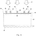
- Fig. 6 illustrates the step of forming the metal film 43.
- the resist 41 and the to-be-exposed resist 42 illustrated in Fig. 5 are developed.
- the exposed resist is exposed to the developing solution along with the transparent base plate 28.
- an alkaline developing solution suitable for the material used in the resist 41 may be used.
- an immersion method, a shaking method, a paddle method, a spray method, or the like can be used.
- the resists are rinsed with pure water and then dried.
- a metal film 48 is formed on the top surface 39 on which the resist pattern 45 has been s formed.
- the formation of the metal film 48 may be performed by any one of, but not limited to, evaporation, sputtering, and electroforming.
- the resist pattern 45 illustrated in Fig. 6 is removed from the transparent base member 28.
- the aperture array 24 composed of the metal film 48 ( Fig. 6 ) is formed as illustrated in Fig. 7 .
- the aperture 26 as illustrated in Fig. 2 is formed in the portion where the to-be-exposed resist 42 is removed.
- the screen 20 can be manufactured.
- the removal of the resist pattern 45 illustrated in Fig. 6 is performed by a lift-off process.
- the lift-off it is preferable to bring the solvent into contact with the to-be-exposed resist 42.
- the lift-off solution may be warmed.
- vibration may be applied to the transparent base member 28.
- a vapor deposition method is suitable as a means for forming the metal film 48 illustrated in Fig. 6 .
- metal particles travel straight as a vapor flow 47. Accordingly, the metal particles will not easily reach the side surface of the to-be-exposed resist 42 in a roundabout manner. Accordingly, the side surface of the to-be-exposed resist 42 is not easily covered with the metal film 48.
- the aperture array shields light except for the portion through which the image light 31 passes. This is because the exposure light 44 illustrated in Fig. 5 passes through the portion where the aperture 26 through which the image light 31 illustrated in Fig. 7 passes should formed by the above self-alignment method. Specifically, it is the gist of the resist pattern formation in accordance with this embodiment that the to-be-exposed resist 42 is provided at a portion where the aperture 26 is to be formed by the above self-alignment method.
- a screen is manufactured by the above self-alignment method, and a head up display can be manufactured by arranging such a screen in a head up display.
- the screen 20 is arranged such that the image light 31 is projected from the microlens array 21 side to the screen 20 illustrated in Fig. 7 .
- the transmission of the image light 31 at the aperture 26 takes place efficiently. This is because the aperture 26 is precisely provided in advance at the position through which the image light 31 passes by the self-alignment method.
- At least one of the exposure light 44 illustrated in Fig. 5 and the image light 31 illustrated in Fig. 7 may be adjusted. Specifically, it may be adjusted such that the image point distance Ex of the exposure light 44 illustrated in Fig. 5 and the image point distance Im of the image light 31 illustrated in Fig. 7 are equal to each other. Alternatively, the difference between these image point distances is preferably in any one of the range of 10, 9, 8, 7, 6, 5, 4, 3, 2, and 1%.
- the inner diameter of the aperture 26 illustrated in Fig. 7 can be made substantially equal to the diameter of the spread of the image light 31 on the cross section at the aperture 26. It is made possible to increase the efficiency of reflection of the external light 34 at the light shielding portion 25 while reducing the image light 31 reflected by the inner surface 29 of the light shielding portion 25.
- the transmission efficiency of the image light and the reflection efficiency of the external light can be balanced in accordance with the design of the optical system of the head-up display illustrated in Fig. 3 , i.e., the design of the optical system 30 illustrated in Fig. 3 . Accordingly, adjustment can be implemented depending on the requirements based on the design of the head-up display such that both increase in the transmission efficiency of the image light and increase in the contrast can be achieved in a compatible manner.
- the image point 50 is an image point of the exposure light 44 with respect to the microlens of the microlens array 21.
- the image point 50 is in front of the applied resist 41 with respect to the microlens.
- the image point 50 is in the transparent base member 28, but in other aspects, the image point 50 may be in the microlens array 21.
- the to-be-exposed resist 42 illustrated in Fig. 6 becomes thicker as it becomes more distant from the microlens array 21.
- the to-be-exposed resist 42 has a so-called reverse tapered shape. This is because the exposure light 44 has already passed the image point 50 at the time when the exposure light 44 reaches the to-be-exposed resist 42 as illustrated in Fig. 5 , and the exposure light 44 is in the course of diffusion.
- the angle of the vapor flow 47 to the top surface 39 is not limited. This is because the side face of the to-be-exposed resist 42 having the inverse tapered shape will always be shaded from the vapor flow 47 in any direction.
- the direction of the vapor flow 47 impinging on the top surface 39 illustrated in Fig. 6 is not inclined with respect to the normal direction of the top surface 39.
- the direction of the vapor flow 47 may be inclined by 0° to 20°.
- the range of such inclination is preferably 0° to 10° and more preferably 0° to 5°. When the inclination becomes smaller, the metal film 46 can be thickened more efficiently.
- the positional relationship between the image point 50 illustrated in Fig. 5 and the applied resist 41 can be adjusted as appropriate. Such a positional relationship can be adjusted by, for example, the thickness of at least either one of the transparent base member 28 and the base portion 19 of the microlens array 21. However, when the sum of these thicknesses increases and the image point distance Ex of the image point 50 does not change, then the distance from the main surface of the microlens array 21 to the resist 41 becomes relatively large. In the figure, the image point distance Ex of the image point 50 also takes into account the fact that the exposure light 44 is refracted at the interface between the microlens array 21 and the transparent base member 28. This also applies to the image point distance Im of the image light 31 illustrated in Fig. 7 .
- Fig. 8 illustrates another aspect of the exposure of the resist.
- the exposure light 44 diffused by each microlens is partially omitted for convenience of explanation.
- the distance between the main surface of the microlens array 21 and the resist 41 becomes relatively small when the total thickness of the transparent base member 28 and the base portion 19 becomes small and the image point distance Ex of the image point 50 does not change.
- the image point of the exposure light 44 with respect to the microlens of the microlens array 21 is farther than the resist 41 with respect to the microlens.
- the image point distance Ex of the image point 50 also takes into account the fact that the exposure light 44 is refracted by the transparent base member 28 and the resist 41.
- the to-be-exposed resist 42 illustrated in Fig. 8 tapers away from the microlens array 21.
- the to-be-exposed resist 42 has a so-called forward tapered shape. This is because the exposure light 44 has not yet passed the image point at the time when the exposure light 44 reaches the to-be-exposed resist 42 as illustrated in the figure, and the exposure light 44 is in the course of convergence.
- a portion exposed is generated on the side surface of the to-be-exposed resist 42, where the exposed portion is not coated with the metal film 48.
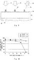
- the magnitude of the inclination in the direction of the vapor flow 51 impinging on the top surface 39 is indicated by the vapor deposition angle Va with reference to the normal direction of the top surface 39. If the vapor deposition angle Va exceeds 60°, the shaded portion of the to-be-exposed resist 42 in the top surface 39 may become large. For this reason, a sufficient amount of metal for forming the light shielding portion cannot be fed to the shaded portion.
- the graph of Fig. 10 illustrates the relationship between the vapor deposition angle Va and the light blocking ratio of the aperture array.
- the graph indicates the light blocking ratio of the aperture array when vapor deposition is performed while changing the deposition angle Va with respect to the top surface 39 illustrated in Fig. 9 .
- the to-be-exposed resist 42 has a substantially cylindrical shape with a diameter of 10 ⁇ m.
- the pitch of the apertures of the aperture array formed on the basis of the to-be-exposed resist 42 is 20 ⁇ m.
- the light blocking ratio illustrated in Fig. 10 indicates the ratio of the area where the metal film is formed on the top surface 39 illustrated in Fig. 9 .
- the height of the to-be-exposed resist 42 is either 1 ⁇ m or 5 ⁇ m. In the case of a height of 5 ⁇ m as compared with the case of a height of 1 ⁇ m, the shaded portion of the to-be-exposed resist 42 becomes large. Accordingly, in the case of a height of 5 ⁇ m, the light blocking ratio is smaller than in the case of a height of 1 ⁇ m. When the height of the to-be-exposed resist 42 is 5 ⁇ m, the light blocking ratio sharply decreases when the deposition angle Va is larger than 60°.
- the graph of Fig. 11 illustrates the relationship between the vapor deposition angle Va and the exposure ratio of the resist.
- the exposure ratio of the resist represents the exposure ratio with reference to the area of the side surface of the to-be-exposed resist 42 illustrated in Fig. 9 .
- the deposition angle Va By setting the deposition angle Va to be larger than 0°, the side surface of the to-be-exposed resist 42 can be exposed.
- the vapor deposition angle Va illustrated in Fig. 9 can be determined by taking:
- the vapor deposition angle Va illustrated in Fig. 9 can be set within the range of 20° to 60°.
- the vapor deposition angle Va is preferably 45°.
- the lift-off can be efficiently performed by suppressing the deposition of metal on the side surface of the to-be-exposed resist 42. Further, it is made possible to efficiently deposit the metal on the top surface 39 where the light shielding portion is to be formed.
- the present disclosure is not limited to the above-described embodiment and can be appropriately modified without departing from the spirit of the invention.
- the transparent base member 28 and the microlens array 21 illustrated in Fig. 1 may be shaped as a seamless integral member.
- a microlens array sheet including the transparent base member 28 and the microlens array 21 illustrated in Fig. 4 was formed.
- the microlens array 21 was shaped on the transparent base member 28 made of a polycarbonate film using ultraviolet curable resin.
- the thickness of the polycarbonate film was 100 ⁇ m.
- An acrylic resin was used as ultraviolet curable resin.
- the irradiation amount of ultraviolet ray was 500 mJ/cm 2 .
- the resist 41 was applied to the back side of the microlens array sheet, i.e., the top surface 39. Coating was carried out by a spin coating method. The number of revolutions of the microlens array sheet as a workpiece was adjusted so that the film thickness of the resist 41 was 5 ⁇ m.
- PMER N-CA 3000 which is a negative type photoresist manufactured by TOKYO OHKA KOGYO CO., LTD. was used. The resist 41 was dried in an oven at 70°C for 20 minutes.
- the microlens array sheet was set on the stage of a UV exposure apparatus. At this point, the microlens array 21 illustrated in Fig. 5 was placed as the upper side. Ultraviolet rays were emitted from the microlens array 21 side. The exposure amount was 500 mJ/cm 2 . After the exposure, the microlens array sheet was subjected to PEB (post exposure bake) treatment in an oven at 70°C for 20 minutes.
- PEB post exposure bake
- the microlens array sheet was immersed in an organic alkaline developing solution (TMAH 2.38%). Also, the microlens array sheet was shaken for 3 minutes. The microlens array sheet taken out from the developer was rinsed with pure water and further dried.
- TMAH organic alkaline developing solution
- the metal film 48 illustrated in Fig. 6 was formed by a vacuum deposition apparatus, where the vapor deposition angle was 45°.
- the weight of the vapor deposition source was 10.4 g.
- the thickness of the vapor-deposited film was about 200 nm.
- the lift-off was carried out by immersing the vapor-deposited microlens array sheet in NMP (n-methyl-2-pyrrolidone).
- NMP n-methyl-2-pyrrolidone
- the microlens array sheet was shaken for 180 seconds.
- the to-be-exposed resist 42 was melted to form the aperture array 24 illustrated in Fig. 7 .
- the screen of the example was obtained.
- the screen taken out from the NMP was rinsed with pure water and air-dried.
- the item that has undergone the processes up to shaping of the microlens array by ultraviolet curable resin according to the example was defined as the screen of a comparative example.
- the reflection characteristics on the back side of the microlens array sheet, i.e., on the top surface 39 side illustrated in Fig. 7 were evaluated.
- Fig. 12 is a schematic diagram of an apparatus for evaluating the reflection characteristics.
- This apparatus is a goniometer for measuring the intensity distribution of the reflected light according to the reflection angles when the test screen 60 is irradiated with the external light 64.
- the test screen 60 was placed on the black sheet 59 with the microlens array as the lower side.
- LED quasi-parallel light having a divergence angle of 5° or less was used as the external light 64 illustrated in Fig. 12 .
- a light source 61 that emits such a parallel light was arranged.
- a part of the external light 64 is diffusely reflected on the test screen 60 and becomes diffuse reflection light 65.
- a part of the external light 64 is specularly reflected by the test screen 60 and becomes specular reflection light 66.
- the specular reflection light 66 is inclined by +20°.
- the intensities of the diffuse reflection light 65 and the specular reflection light 66 illustrated in Fig. 12 were measured using the 2-D luminance meter 62.
- the reflection angle was changed by changing the observation angle Ob of the 2-D luminance meter 62 from -60° to +60°.
- the observation angle Ob when the 2-D luminance meter 62 faces the test screen 60 directly was set to 0°.
- the mounting angle of the test screen 60 when the test screen 60 is installed in the head-up display is 20°. Accordingly, the optical axis of the light source 61 is out of alignment by -20° with the optical axis of the 2-D luminance meter 62 at the observation angle Ob of 0°.
- Fig. 13 is a graph showing the correlation between the brightness of the diffuse reflection light and the observation angle.
- the unit of the brightness of diffuse reflected light is cd/m 2 .
- the inclination angle when the screen is attached to the head-up display is 20°. Accordingly, strong specularly reflected light is prevented from entering the observer's eyes.
Landscapes
- Physics & Mathematics (AREA)
- General Physics & Mathematics (AREA)
- Optics & Photonics (AREA)
- Optical Elements Other Than Lenses (AREA)
- Overhead Projectors And Projection Screens (AREA)
- Devices For Indicating Variable Information By Combining Individual Elements (AREA)
Abstract
Description
- The present disclosure relates to a screen for display, and in particular to a transmissive screen.
-
Patent Literature 1 discloses a transmissive screen for a head-up display (HUD). Such a screen includes a microlens array positioned on the incident side of laser light and an aperture array positioned on the output side (Claim 1 of Patent Literature 1). The light shielding portion of the aperture array is formed of a material that absorbs visible light such as a black resist (paragraph [0052] of Patent Literature 1). - The head up display of
Patent Literature 1 can absorb external light reaching the screen by the light shielding portion (paragraph [0054] of the same Literature). Accordingly, the contrast of the displayed image can be enhanced by reducing the external light reflection on the screen (paragraph [0056] of the same Literature). - Patent Literature 1: Japanese Unexamined Patent Application Publication No.
2012-208440 - The light shielding portion of the above-described aperture array absorbs external light. Accordingly, the light shielding portion acts as a heat collector for the external light. As a result, overheating of the light shielding part may cause overheating of the entire screen.
-
- (1) A transmissive screen including a microlens array,
the screen further including an aperture array disposed on a surface opposite to a surface on which the microlens array is disposed, in which
a light shielding portion of the aperture array is a metal film. - (2) The screen recited in item (1), wherein the metal film is a vapor-deposited film.
- (3) The screen recited in item (1) or (2), wherein an outer surface of the metal film has a mirror surface.
- (4) The screen recited in any one of items (1) to (3), wherein the outer surface of the metal film has a reflectance of 80% or more of light having a wavelength of 380 nm to 780 nm.
- (5) A head-up display including the screen recited in any one of items (1) to (4), wherein
an image light is projected onto the screen from the microlens array side, and
an inner diameter of an aperture of the aperture array is equal to or larger than a diameter of spread of the image light on a cross section at the aperture. - (6) A head-up display including the screen recited in any one of items (1) to (4), wherein
the screen is tilted such that the screen is inclined with respect to an optical axis of the image light projected onto the screen from the microlens array side,
the head-up display further including a light absorbing portion absorbing an external light reflected by the light shielding portion. - (7) A method of manufacturing a transmissive screen including a microlens array and an aperture array disposed on an opposite side of the microlens array, the method including, in forming the aperture array on a transparent base member on one side of which the microlens array is formed, the steps of:
- applying a negative resist to an opposite surface of the transparent base member on one surface of which the microlens array is disposed;
- irradiating the transparent base member with an exposure light, the exposure light being emitted toward the transparent base member from the microlens array side;
- exposing the negative resist with the exposure light and further developing the negative resist to form a resist pattern;
- forming a metal film on a surface of the transparent base member on which the resist pattern has been formed; and
- removing the resist pattern to form the aperture array made of the metal film.
- (8) The method for manufacturing the screen recited in item (7), wherein
an image point of the exposure light with respect to a microlens of the microlens array is in front of the coated negative resist with respect to the microlens,
the metal film is formed by vapor deposition, and
the resist pattern is removed by lift-off. - (9) The method for manufacturing the screen recited in item (8), wherein in the vapor deposition, a direction of a vapor flow impinging on a surface of the transparent base member is not inclined or is inclined by 0° to 20° with respect to a normal direction of the surface of the transparent base member.
- (10) The method for manufacturing the screen recited in item (7), wherein
an image point of the exposure light with respect to the microlens of the microlens array is farther from the microlens than the coated negative resist,
the metal film is formed by vapor deposition,
the resist pattern is removed by lift-off, and
in the vapor deposition, a direction of a vapor flow impinging on a surface of the transparent base member is inclined by 20° to 60° with respect to a normal direction of the surface of the transparent base member. - (11) A method of manufacturing a head-up display whose screen is produced by the method recited in any one of items (7) to (10) and arranged such that an image light is projected from the microlens array side to the screen, wherein
at least one of the exposure light and the image light is adjusted so that an image point distance of the exposure light with respect to the microlens of the microlens array is equal to an image point distance of the image light. - According to the present disclosure, it is made possible to suppress overheating of a transmission type screen.
-
- [
Fig. 1] Fig. 1 is a cross-sectional view of a screen. - [
Fig. 2] Fig. 2 is a captured image of an aperture array. - [
Fig. 3] Fig. 3 is a schematic diagram of an optical system of a head-up display. - [
Fig. 4] Fig. 4 is a schematic diagram of application of a resist. - [
Fig. 5] Fig. 5 is a schematic view of exposure of the resist. - [
Fig. 6] Fig. 6 is a schematic diagram of formation of a metal film. - [
Fig. 7] Fig. 7 is a schematic diagram of a light incident to the screen. - [
Fig. 8] Fig. 8 is a schematic view of exposure of the resist. - [
Fig. 9] Fig. 9 is a schematic diagram of formation of a metal film. - [
Fig. 10] Fig. 10 is a graph showing the correlation between vapor deposition angle and light blocking ratio of the aperture array. - [
Fig. 11] Fig. 11 is a graph showing the correlation between vapor deposition angle and exposure ratio. - [
Fig. 12] Fig. 12 is a schematic diagram of an apparatus for evaluating reflection characteristics. - [
Fig. 13] Fig. 13 is a graph showing the correlation between an intensity of a reflected light and an irradiation angle. -
Fig. 1 illustrates a cross-sectional view of atransmissive screen 20. Thescreen 20 includes amicrolens array 21 and anaperture array 24. Theaperture array 24 is arranged on the surface on the other side of the surface on which themicrolens array 21 is arranged. Themicrolens array 21 and theaperture array 24 are arranged on atransparent base member 28 made of resin. - The
screen 20 illustrated inFig. 1 let animage light 31 pass therethrough. At this point,individual microlenses 22 of themicrolens array 21 generatediffusion 32 of theimage light 31. Accordingly, as the orientation of the optical axis of theimage light 31 is dispersed, thescreen 20 functions as an optical screen. In addition, the diffusion angle in thediffusion 32 can be made as desired in accordance with the design of themicrolens 22. The diffusion angle may be defined as a spread angle which represents positions at which a value of luminance of the diffusedimage light 31 becomes equal to a half value of the center luminance of theimage light 31. Themicrolens 22 has a convex surface projecting outward of thescreen 20, i.e., downward in the figure. - The
aperture array 24 illustrated inFig. 1 includes alight shielding portion 25 and anaperture 26. Accordingly, the diffused image light 31 which has been diffused as described above finally passes through thescreen 20 via theaperture 26. In other words, it is preferable that thelight shielding portion 25 is provided only in the portions other than the portion through which the image light 31 passes. - It is preferable that the inner diameter of the
aperture 26 illustrated inFig. 1 is equal to or larger than the diameter of the spread of theimage light 31 on the cross section of theimage light 31 at theaperture 26. For example, it is so designed in a head-up display that includes thescreen 20. According to such an aspect, theimage light 31 reflected by aninner surface 29 of thelight shielding portion 25 can be reduced. Theinner surface 29 is a surface of thelight shielding portion 25 and located on the top surface side of thetransparent base member 28, i.e., the surface opposite anouter surface 27. -
Fig. 2 is an image obtained by capturing one example of theaperture array 24. As illustrated in the captured image,apertures 26 are arranged in a lattice pattern on theaperture array 24. Theaperture 26 is surrounded by thelight shielding portion 25. Thelight shielding portion 25 is a metal film. It is preferable that the metal film is a film formed by any one of vapor deposition, sputtering, and electroforming. It is preferable that the metal film is a vapor-deposited film. - Referring again to
Fig. 1 , it is preferable that theouter surface 27 of the metal film constituting thelight shielding portion 25 has a mirror surface. In thelight shielding portion 25, theouter surface 27 is the surface farther from themicrolens array 21. On theouter surface 27, the reflectance of light having a wavelength of 380 nanometers (nm) to 780 nm is preferably 80% or more, more preferably 83% or more, and further preferably 87% or more. - The reflectance of the
outer surface 27 illustrated inFig. 1 is obtained, for example, from a value resulting when irradiating a metal film with light, the metal film being fabricated in the same manner as thelight shielding portion 25 and having no aperture and measuring the brightness of the reflected light using a spectrophotometer. In this measurement, it is preferable that the incident light is incident on theouter surface 27 at an angle of 10 degrees with respect to the normal line of theouter surface 27. For example, U-4100 manufactured by Hitachi High-Tech Science Corporation may be used as the spectrophotometer. - An
optical system 30 of the head-up display is illustrated inFig. 3 . Such a head-up display includes thescreen 20. Thescreen 20 constitutes a part of theoptical system 30. - The
image light 31 indicated by the solid line inFig. 3 is projected onto thescreen 20 from themicrolens array 21 side. Theimage light 31 is generated by, for example, a picture generation unit (PGU). Theimage light 31 is guided to thescreen 20 by a projection optical system. - The
image light 31 illustrated inFig. 3 is diffused by themicrolens array 21. The image light 31 passes through thescreen 20. Theimage light 31 is emitted from thescreen 20 as diffused light and is reflected by aconcave mirror 35. Thereafter, theimage light 31 is presented as an image of a virtual image to an observer viewing the head-up display. - As illustrated in
Fig. 3 , thescreen 20 includes themicrolens array 21. By virtue of this, the diffusion angle, efficiency, and the like of thescreen 20 can be readily controlled by themicrolens array 21. In addition, use of themicrolens array 21 makes it possible to adjust the image presented by theimage light 31 so that it has an angle of view at which the observer can readily view the image. - Here, let us consider a case where the head-up display is mounted in a vehicle and the vehicle is arranged outdoors. In this case, sunlight may enter the
optical system 30 illustrated inFig. 3 as anexternal light 34. Theexternal light 34 indicated by the broken line inFig. 3 is reflected by theconcave mirror 35. In addition, after the reflection, theexternal light 34 may reach thescreen 20. - When the
screen 20 illustrated inFig. 3 is arranged on a plane perpendicular to the optical axis of theimage light 31, theexternal light 34 entering from the opposite direction to theimage light 31 is reflected by thescreen 20. Specifically, it is reflected by themicrolens array 21 or theaperture array 24. At this point, since the optical axis of theimage light 31 and the optical axis of theexternal light 34 are parallel to each other, there is a possibility that theexternal light 34 is mixed with theimage light 31. - When the
external light 34 is mixed with theimage light 31 illustrated inFig. 3 , the image presented by theimage light 31 is whitened. Accordingly, the contrast of the image is lowered. For an observer, for example, a driver of a vehicle, not only the visibility of the image is deteriorated but also glaring portions are visually recognized in the image. Such a problem is not limited to the case where theexternal light 34 is sunlight. The same problem arises in any other cases where the head-up display is not mounted on a vehicle. - In accordance with this embodiment, as illustrated in
Fig. 3 , thescreen 20 is inclined so that the optical axis of theimage light 31 emitted from theaperture 26 is not parallel to the optical axis of theexternal light 34 reflected by thelight shielding portion 25. Thescreen 20 is inclined such that thescreen 20 is inclined with respect to the optical axis of theimage light 31 projected on thescreen 20 from themicrolens array 21 side. As a result, the entering external light 34 can escape in a direction different from the optical axis of theimage light 31. Accordingly, since theexternal light 34 is not easily mixed with theimage light 31, whitening of the image is suppressed. - As illustrated in
Fig. 3 , the head up display in accordance with this embodiment further includes alight absorbing portion 36. Theexternal light 34 reflected by thelight shielding portion 25 strikes thelight absorbing portion 36. Thelight absorbing portion 36 is subjected to black painting, alumite treatment, and the like. Thelight absorbing portion 36 absorbs theexternal light 34. Accordingly, occurrence of a phenomenon where theexternal light 34 becomes stray light in theoptical system 30 is suppressed. - As described in the background art section, even if a black matrix like a black resist is used as a substitute for the
light shielding portion 25, the contrast of the image can be enhanced. However, since theexternal light 34 illustrated inFig. 3 is collected on the screen by theconcave mirror 35, the energy of theexternal light 34 is efficiently absorbed with the black matrix. Accordingly, the screen may be easily overheated along with the black matrix. - Here, when the screen is made of a transparent base member made of resin, deformation or ignition of the screen may be caused. For this reason, an absorptive type contrast enhancing means such as a black matrix is not suitable for the screen in a head-up display. Such a problem is not limited to the case where the
external light 34 is sunlight. The same problem may arise even in any other case where the head-up display is not mounted in a vehicle. - On the other hand, in accordance with this embodiment, as illustrated in
Fig. 3 , theexternal light 34 that has reached thescreen 20 can escape to thelight absorbing portion 36. This is because thescreen 20 is provided with thelight shielding portion 25 made of a metal film. Thelight shielding portion 25 reflects theexternal light 34 by regular reflection. As a result, thelight shielding portion 25 is not easily overheated and accordingly thescreen 20 is not easily overheated. - The
microlens array 21 illustrated inFig. 1 can be formed as a sheet in accordance with a known method. The mold used to shape the microlens array sheet may be formed by cutting. In addition, a template may be formed by photolithography to form the mold on the basis of such a template. The mold may be fabricated by laser ablation. Any mold can be used as long as it can withstand the shaping of the microlens array sheet. - In the shaping of the
microlens array 21 illustrated inFig. 1 , various means suitable for shaping a resin sheet, such as injection molding, press molding, and shaping by ultraviolet curing, can be used. Further, the sheet obtained by shaping may be attached to thetransparent base member 28. Further, a resin disposed on thetransparent base member 28 may be shaped. - In the meantime, in forming the aperture array, it is necessary to pay attention to the following aspect. Specifically, as illustrated in
Fig. 3 , theaperture array 24 blocks theexternal light 34 but does not block theimage light 31. Accordingly, it is necessary to accurately form a pattern of the aperture array on thetransparent base member 28 in accordance with the arrangement of themicrolenses 22 in themicrolens array 21. - It is preferable in this embodiment to use self-alignment exposure as the pattern forming method. In the self-alignment exposure, a photoresist is exposed using the light collection function of the
microlens array 21 as such illustrated inFigs. 1 and3 . When the self-alignment exposure is used, it is preferable to combine a lift-off method to selectively remove an unnecessary metal film so as to form theaperture 26. - The method of forming the aperture array on the
transparent base member 28 will be described with reference toFigs. 4 to 8 .Fig. 4 is a schematic diagram of resist application. Themicrolens array 21 is formed on one side of thetransparent base member 28, i.e., thebottom surface 38. The resist 41 is applied to thetop surface 39 of thetransparent base member 28. Thetop surface 39 is a surface opposite to thebottom surface 38. The resist 41 is a negative resist. It is preferable that the resist 41 comprises a photosensitive resin. - Spin coating, die coating, spray coating, roll coating, and the like can be used as the method of coating the resist 41 on the
top surface 39 illustrated inFig. 4 . Further, drying is performed to volatilize the solvent of the applied resist 41. For drying, a hot plate, oven, vacuum dryer, infrared heater, and the like can be used. As a method that does not involve application and drying, a method of laminating a film resist can be adopted. -
Fig. 5 is a schematic view of exposure of the resist. Anexposure light 44 is emitted from the side of themicrolens array 21 toward thetransparent base member 28. It is preferable that theexposure light 44 is ultraviolet light. Theexposure light 44 is collected by each microlens of themicrolens array 21. The resist 41 is exposed by theexposure light 44. In this case, if multiple types of microlenses are included in themicrolens array 21, the aperture diameter may change according to the focal length and diffusion angle of the microlens. - As the
exposure light 44 illustrated inFig. 5 , it is possible to use light containing wavelengths that can cause the resist 41 to be exposed. It is preferable that the light source of theexposure light 44 is a light source capable of emitting light having substantially the same projection angle and pupil diameter as those of theimage light 31 illustrated inFig. 3 . It is also preferable that the light source of theexposure light 44 is a light source having a small viewing angle. - Implementation of the self-alignment exposure as described above is suitable for transmitting the exposure light through substantially the same optical path as the optical path of the
image light 31 as illustrated inFig. 7 which will be described later. Specifically, if the resist 41 illustrated inFig. 4 is irradiated with the image light, the implementation is suitable for exposing only the portion of the resist 41 which is considered to allow the image light to pass through. The resist 41 in such a portion changes to the to-be-exposed resist 42 illustrated inFig. 5 . -
Fig. 6 illustrates the step of forming the metal film 43. Before forming the metal film 43, the resist 41 and the to-be-exposed resist 42 illustrated inFig. 5 are developed. Upon development, the exposed resist is exposed to the developing solution along with thetransparent base plate 28. As the developing solution, an alkaline developing solution suitable for the material used in the resist 41 may be used. As the development method, an immersion method, a shaking method, a paddle method, a spray method, or the like can be used. After the development, the resists are rinsed with pure water and then dried. - As described above, the unexposed portion of the resist 41 is removed. Thereafter, a resist
pattern 45 illustrated inFig. 6 is formed. Ametal film 48 is formed on thetop surface 39 on which the resistpattern 45 has been s formed. The formation of themetal film 48 may be performed by any one of, but not limited to, evaporation, sputtering, and electroforming. - The resist
pattern 45 illustrated inFig. 6 is removed from thetransparent base member 28. By removal of the resistpattern 45, theaperture array 24 composed of the metal film 48 (Fig. 6 ) is formed as illustrated inFig. 7 . Theaperture 26 as illustrated inFig. 2 is formed in the portion where the to-be-exposed resist 42 is removed. Thus, thescreen 20 can be manufactured. - It is preferable that the removal of the resist
pattern 45 illustrated inFig. 6 is performed by a lift-off process. In the lift-off, it is preferable to bring the solvent into contact with the to-be-exposed resist 42. It is also preferable to remove the resistpattern 45 by immersing the resistpattern 45 together thetransparent base member 28 in the lift-off solution. In order to promote the lift-off, the lift-off solution may be warmed. In order to promote the lift-off, vibration may be applied to thetransparent base member 28. - In the above lift-off process, a portion that is not covered with the
metal film 48 but is exposed needs to exist on the side surface of the to-be-exposed resist 42 illustrated inFig. 6 . From the above viewpoint, a vapor deposition method is suitable as a means for forming themetal film 48 illustrated inFig. 6 . In the vapor deposition method, metal particles travel straight as avapor flow 47. Accordingly, the metal particles will not easily reach the side surface of the to-be-exposed resist 42 in a roundabout manner. Accordingly, the side surface of the to-be-exposed resist 42 is not easily covered with themetal film 48. - As illustrated in
Fig. 7 , the aperture array shields light except for the portion through which the image light 31 passes. This is because theexposure light 44 illustrated inFig. 5 passes through the portion where theaperture 26 through which theimage light 31 illustrated inFig. 7 passes should formed by the above self-alignment method. Specifically, it is the gist of the resist pattern formation in accordance with this embodiment that the to-be-exposed resist 42 is provided at a portion where theaperture 26 is to be formed by the above self-alignment method. - In accordance with this embodiment, a screen is manufactured by the above self-alignment method, and a head up display can be manufactured by arranging such a screen in a head up display.
- At this point, the
screen 20 is arranged such that theimage light 31 is projected from themicrolens array 21 side to thescreen 20 illustrated inFig. 7 . In the head-up display manufactured by such a method, the transmission of theimage light 31 at theaperture 26 takes place efficiently. This is because theaperture 26 is precisely provided in advance at the position through which the image light 31 passes by the self-alignment method. - Further, according to the method of manufacturing a head-up display using the self-alignment method, at least one of the
exposure light 44 illustrated inFig. 5 and theimage light 31 illustrated inFig. 7 may be adjusted. Specifically, it may be adjusted such that the image point distance Ex of theexposure light 44 illustrated inFig. 5 and the image point distance Im of theimage light 31 illustrated inFig. 7 are equal to each other. Alternatively, the difference between these image point distances is preferably in any one of the range of 10, 9, 8, 7, 6, 5, 4, 3, 2, and 1%. - As described above, the inner diameter of the
aperture 26 illustrated inFig. 7 can be made substantially equal to the diameter of the spread of theimage light 31 on the cross section at theaperture 26. It is made possible to increase the efficiency of reflection of theexternal light 34 at thelight shielding portion 25 while reducing theimage light 31 reflected by theinner surface 29 of thelight shielding portion 25. - According to the above aspect, the transmission efficiency of the image light and the reflection efficiency of the external light can be balanced in accordance with the design of the optical system of the head-up display illustrated in
Fig. 3 , i.e., the design of theoptical system 30 illustrated inFig. 3 . Accordingly, adjustment can be implemented depending on the requirements based on the design of the head-up display such that both increase in the transmission efficiency of the image light and increase in the contrast can be achieved in a compatible manner. - Referring again to
Fig. 5 , theimage point 50 is an image point of theexposure light 44 with respect to the microlens of themicrolens array 21. Theimage point 50 is in front of the applied resist 41 with respect to the microlens. In the figure, theimage point 50 is in thetransparent base member 28, but in other aspects, theimage point 50 may be in themicrolens array 21. - Here, the to-be-exposed resist 42 illustrated in
Fig. 6 becomes thicker as it becomes more distant from themicrolens array 21. The to-be-exposed resist 42 has a so-called reverse tapered shape. This is because theexposure light 44 has already passed theimage point 50 at the time when theexposure light 44 reaches the to-be-exposed resist 42 as illustrated inFig. 5 , and theexposure light 44 is in the course of diffusion. - When the
vapor flow 47 illustrated inFig. 6 is sprayed from one direction to thetop surface 39, the angle of thevapor flow 47 to thetop surface 39 is not limited. This is because the side face of the to-be-exposed resist 42 having the inverse tapered shape will always be shaded from thevapor flow 47 in any direction. - Accordingly, it is preferable that the direction of the
vapor flow 47 impinging on thetop surface 39 illustrated inFig. 6 is not inclined with respect to the normal direction of thetop surface 39. Also, the direction of thevapor flow 47 may be inclined by 0° to 20°. The range of such inclination is preferably 0° to 10° and more preferably 0° to 5°. When the inclination becomes smaller, the metal film 46 can be thickened more efficiently. - The positional relationship between the
image point 50 illustrated inFig. 5 and the applied resist 41 can be adjusted as appropriate. Such a positional relationship can be adjusted by, for example, the thickness of at least either one of thetransparent base member 28 and thebase portion 19 of themicrolens array 21. However, when the sum of these thicknesses increases and the image point distance Ex of theimage point 50 does not change, then the distance from the main surface of themicrolens array 21 to the resist 41 becomes relatively large. In the figure, the image point distance Ex of theimage point 50 also takes into account the fact that theexposure light 44 is refracted at the interface between themicrolens array 21 and thetransparent base member 28. This also applies to the image point distance Im of theimage light 31 illustrated inFig. 7 . - When the distance from the main surface of the
microlens array 21 to the resist 41 becomes significantly larger than the image point distance Ex of theimage point 50 as described above, there is a possibility that theexposure light 44 diffused at each of the adjacent microlenses in themicrolens array 21 may overlap with each other in the resist 41. In this case, most of the resist 41 is exposed. Accordingly, theaperture 26 surrounded by thelight shielding portion 25 as illustrated inFig. 2 , cannot be formed. As a result, theaperture array 24 illustrated inFig. 3 cannot efficiently reflect theexternal light 34. -
Fig. 8 illustrates another aspect of the exposure of the resist. Theexposure light 44 diffused by each microlens is partially omitted for convenience of explanation. The distance between the main surface of themicrolens array 21 and the resist 41 becomes relatively small when the total thickness of thetransparent base member 28 and thebase portion 19 becomes small and the image point distance Ex of theimage point 50 does not change. In the drawing, the image point of theexposure light 44 with respect to the microlens of themicrolens array 21 is farther than the resist 41 with respect to the microlens. InFig. 8 , the image point distance Ex of theimage point 50 also takes into account the fact that theexposure light 44 is refracted by thetransparent base member 28 and the resist 41. - In the above case, the to-be-exposed resist 42 illustrated in
Fig. 8 tapers away from themicrolens array 21. The to-be-exposed resist 42 has a so-called forward tapered shape. This is because theexposure light 44 has not yet passed the image point at the time when theexposure light 44 reaches the to-be-exposed resist 42 as illustrated in the figure, and theexposure light 44 is in the course of convergence. - In this case, there is a possibility that a problem arises in the lift-off described above. As illustrated in
Fig. 8 , when the to-be-exposed resist 42 is forwardly tapered, the lift-off of the resist pattern may not able to be performed. As illustrated inFig. 9 , when vapor deposition is performed so that thevapor flow 47 perpendicular to thetop surface 39 is sprayed, the to-be-exposed resist 42 is completely covered with the metal particles. This is because no portion can be formed which is shaded from thevapor flow 47 on the side surface of the to-be-exposed resist 42. - In the above case, by inclining the vapor flow like the
vapor flow 51 as illustrated inFig. 9 a portion exposed is generated on the side surface of the to-be-exposed resist 42, where the exposed portion is not coated with themetal film 48. The magnitude of the inclination in the direction of thevapor flow 51 impinging on thetop surface 39 is indicated by the vapor deposition angle Va with reference to the normal direction of thetop surface 39. If the vapor deposition angle Va exceeds 60°, the shaded portion of the to-be-exposed resist 42 in thetop surface 39 may become large. For this reason, a sufficient amount of metal for forming the light shielding portion cannot be fed to the shaded portion. - The graph of
Fig. 10 illustrates the relationship between the vapor deposition angle Va and the light blocking ratio of the aperture array. The graph indicates the light blocking ratio of the aperture array when vapor deposition is performed while changing the deposition angle Va with respect to thetop surface 39 illustrated inFig. 9 . The to-be-exposed resist 42 has a substantially cylindrical shape with a diameter of 10 µm. The pitch of the apertures of the aperture array formed on the basis of the to-be-exposed resist 42 is 20 µm. - The light blocking ratio illustrated in
Fig. 10 indicates the ratio of the area where the metal film is formed on thetop surface 39 illustrated inFig. 9 . The height of the to-be-exposed resist 42 is either 1 µm or 5 µm. In the case of a height of 5 µm as compared with the case of a height of 1 µm, the shaded portion of the to-be-exposed resist 42 becomes large. Accordingly, in the case of a height of 5 µm, the light blocking ratio is smaller than in the case of a height of 1 µm. When the height of the to-be-exposed resist 42 is 5 µm, the light blocking ratio sharply decreases when the deposition angle Va is larger than 60°. - The graph of
Fig. 11 illustrates the relationship between the vapor deposition angle Va and the exposure ratio of the resist. The exposure ratio of the resist represents the exposure ratio with reference to the area of the side surface of the to-be-exposed resist 42 illustrated inFig. 9 . There is almost no difference in the exposure ratio between the case where the height of the to-be-exposed resist 42 is 1 µm and the case where it is 5 µm, By setting the deposition angle Va to be larger than 0°, the side surface of the to-be-exposed resist 42 can be exposed. - From the above, the vapor deposition angle Va illustrated in
Fig. 9 can be determined by taking: - the thickness of the vapor:
- the size of the portion to be exposed on the side surface of the to-be-exposed resist 42; and
- the size of the portion of the
top surface 39 which is not vapor-deposited due to being shadowed from the to-be-exposed resist 42
- into account complementary manner.
- Based on the above principle, the vapor deposition angle Va illustrated in
Fig. 9 can be set within the range of 20° to 60°. The vapor deposition angle Va is preferably 45°. By virtue of such a deposition angle Va, the lift-off can be efficiently performed by suppressing the deposition of metal on the side surface of the to-be-exposed resist 42. Further, it is made possible to efficiently deposit the metal on thetop surface 39 where the light shielding portion is to be formed. - It should be noted that the present disclosure is not limited to the above-described embodiment and can be appropriately modified without departing from the spirit of the invention. For example, the
transparent base member 28 and themicrolens array 21 illustrated inFig. 1 may be shaped as a seamless integral member. - A microlens array sheet including the
transparent base member 28 and themicrolens array 21 illustrated inFig. 4 was formed. Themicrolens array 21 was shaped on thetransparent base member 28 made of a polycarbonate film using ultraviolet curable resin. The thickness of the polycarbonate film was 100 µm. An acrylic resin was used as ultraviolet curable resin. The irradiation amount of ultraviolet ray was 500 mJ/cm2. - As illustrated in
Fig. 4 , the resist 41 was applied to the back side of the microlens array sheet, i.e., thetop surface 39. Coating was carried out by a spin coating method. The number of revolutions of the microlens array sheet as a workpiece was adjusted so that the film thickness of the resist 41 was 5 µm. As the resist 41, PMER N-CA 3000 which is a negative type photoresist manufactured by TOKYO OHKA KOGYO CO., LTD. was used. The resist 41 was dried in an oven at 70°C for 20 minutes. - The microlens array sheet was set on the stage of a UV exposure apparatus. At this point, the
microlens array 21 illustrated inFig. 5 was placed as the upper side. Ultraviolet rays were emitted from themicrolens array 21 side. The exposure amount was 500 mJ/cm2. After the exposure, the microlens array sheet was subjected to PEB (post exposure bake) treatment in an oven at 70°C for 20 minutes. - For development, the microlens array sheet was immersed in an organic alkaline developing solution (TMAH 2.38%). Also, the microlens array sheet was shaken for 3 minutes. The microlens array sheet taken out from the developer was rinsed with pure water and further dried.
- The
metal film 48 illustrated inFig. 6 was formed by a vacuum deposition apparatus, where the vapor deposition angle was 45°. The weight of the vapor deposition source was 10.4 g. The thickness of the vapor-deposited film was about 200 nm. The lift-off was carried out by immersing the vapor-deposited microlens array sheet in NMP (n-methyl-2-pyrrolidone). The microlens array sheet was shaken for 180 seconds. As a result, the to-be-exposed resist 42 was melted to form theaperture array 24 illustrated inFig. 7 . Thus, the screen of the example was obtained. The screen taken out from the NMP was rinsed with pure water and air-dried. - The item that has undergone the processes up to shaping of the microlens array by ultraviolet curable resin according to the example was defined as the screen of a comparative example. In the example and the comparative example, the reflection characteristics on the back side of the microlens array sheet, i.e., on the
top surface 39 side illustrated inFig. 7 were evaluated. -
Fig. 12 is a schematic diagram of an apparatus for evaluating the reflection characteristics. This apparatus is a goniometer for measuring the intensity distribution of the reflected light according to the reflection angles when thetest screen 60 is irradiated with theexternal light 64. Thetest screen 60 was placed on theblack sheet 59 with the microlens array as the lower side. - As the
external light 64 illustrated inFig. 12 , LED quasi-parallel light having a divergence angle of 5° or less was used. Alight source 61 that emits such a parallel light was arranged. A part of theexternal light 64 is diffusely reflected on thetest screen 60 and becomes diffusereflection light 65. A part of theexternal light 64 is specularly reflected by thetest screen 60 and becomesspecular reflection light 66. Thespecular reflection light 66 is inclined by +20°. - The intensities of the diffuse
reflection light 65 and the specular reflection light 66 illustrated inFig. 12 were measured using the 2-D luminance meter 62. The reflection angle was changed by changing the observation angle Ob of the 2-D luminance meter 62 from -60° to +60°. The observation angle Ob when the 2-D luminance meter 62 faces thetest screen 60 directly was set to 0°. - In this measurement, it is assumed that the mounting angle of the
test screen 60 when thetest screen 60 is installed in the head-up display is 20°. Accordingly, the optical axis of thelight source 61 is out of alignment by -20° with the optical axis of the 2-D luminance meter 62 at the observation angle Ob of 0°. -
Fig. 13 is a graph showing the correlation between the brightness of the diffuse reflection light and the observation angle. The unit of the brightness of diffuse reflected light is cd/m2. The intensity of the specular reflection light 66 (Fig. 12 ) to be observed when the observation angle Ob is +20° exceeded the upper limit of the graph range. - As illustrated in
Fig. 13 , it was considered that the intensity of specularly reflected light was larger than in the comparative example in the screen of the example. However, in the region of 0° or less, the intensity of the diffuse reflected light was smaller than that in the comparative example. Accordingly, it is considered that internally reflected light generated by reflection of external light reaching the microlens is blocked by the aperture array. - As described above, in this measurement, the inclination angle when the screen is attached to the head-up display is 20°. Accordingly, strong specularly reflected light is prevented from entering the observer's eyes.
- In the case of the screen of the comparative example, it was found that the observer can visually recognize a part of the internally reflected light generated by the microlens. Such internally reflected light lowers the image contrast. Comparison between the comparative example and the example shows that improvement of image contrast can be expected by suppressing the leakage of the internally reflected light by the aperture array of the metal film of this example.
- This application claims priority based on Japanese Patent Application No.
2016-003410 filed on January 12, 2016 - 19 base member, 20 screen, 21 microlens array, 22 microlens, 24 aperture array, 25 light shielding portion, 26 aperture, 27 outer surface, 28 transparent base member, 29 inner surface, 30 optical system, 31 image light, 32 diffusion, 34 external light, 35 concave mirror, 36 light absorbing portion, 38 bottom surface, 39 top surface, 41 resist, 42 to-be-exposed resist, 43 metal film, 44 exposure light, 45 resist pattern, 46 metal film, 47 vapor flow, 48 metal film, 50 image point, 51 vapor flow, 59 sheet, 60 test screen, 61 light source, 62 2-D luminance meter, 64 external light, 65 diffuse reflection light, 66 specular reflection light, Ex image point distance of exposure light, Im image point distance of the image light, Ob observation angle, Va vapor deposition angle
Claims (11)
- A transmissive screen comprising a microlens array,
the screen further comprising an aperture array disposed on a surface opposite to a surface on which the microlens array is disposed, in which
a light shielding portion of the aperture array is a metal film. - The screen according to Claim 1, wherein the metal film is a vapor-deposited film.
- The screen according to Claim 1 or 2, wherein an outer surface of the metal film has a mirror surface.
- The screen according to any one of Claims 1 to 3, wherein the outer surface of the metal film has a reflectance of 80% or more of light having a wavelength of 380 nm to 780 nm.
- A head-up display comprising the screen according to any one of Claims 1 to 4, wherein
an image light is projected onto the screen from the microlens array side, and
an inner diameter of an aperture of the aperture array is equal to or larger than a diameter of spread of the image light on a cross section at the aperture. - A head-up display comprising the screen according to any one of Claims 1 to 4, wherein
the screen is tilted such that the screen is inclined with respect to an optical axis of the image light projected onto the screen from the microlens array side,
the head-up display further comprising a light absorbing portion absorbing an external light reflected by the light shielding portion. - A method of manufacturing a transmissive screen including a microlens array and an aperture array disposed on an opposite side of the microlens array, the method comprising, in forming the aperture array on a transparent base member on one side of which the microlens array is formed, the steps of:applying a negative resist to an opposite surface of the transparent base member on one surface of which the microlens array is disposed;irradiating the transparent base member with an exposure light, the exposure light being emitted toward the transparent base member from the microlens array side;exposing the negative resist with the exposure light and further developing the negative resist to form a resist pattern;forming a metal film on a surface of the transparent base member on which the resist pattern has been formed; andremoving the resist pattern to form the aperture array made of the metal film.
- The method for manufacturing the screen according to Claim 7, wherein
an image point of the exposure light with respect to a microlens of the microlens array is in front of the coated negative resist with respect to the microlens,
the metal film is formed by vapor deposition, and
the resist pattern is removed by lift-off. - The method for manufacturing the screen according to Claim 8, wherein in the vapor deposition, a direction of a vapor flow impinging on a surface of the transparent base member is not inclined or is inclined by 0° to 20° with respect to a normal direction of the surface of the transparent base member.
- The method for manufacturing the screen according to Claim 7, wherein
an image point of the exposure light with respect to the microlens of the microlens array is farther from the microlens than the coated negative resist,
the metal film is formed by vapor deposition,
the resist pattern is removed by lift-off, and
in the vapor deposition, a direction of a vapor flow impinging on a surface of the transparent base member is inclined by 20° to 60° with respect to a normal direction of the surface of the transparent base member. - A method of manufacturing a head-up display whose screen is produced by the method according to any one of claims 7 to 10 and arranged such that an image light is projected from the microlens array side to the screen, wherein
at least one of the exposure light and the image light is adjusted so that an image point distance of the exposure light with respect to the microlens of the microlens array is equal to an image point distance of the image light.
Applications Claiming Priority (2)
| Application Number | Priority Date | Filing Date | Title |
|---|---|---|---|
| JP2016003410 | 2016-01-12 | ||
| PCT/JP2017/000551 WO2017122651A1 (en) | 2016-01-12 | 2017-01-11 | Screen for display |
Publications (2)
| Publication Number | Publication Date |
|---|---|
| EP3404484A1 true EP3404484A1 (en) | 2018-11-21 |
| EP3404484A4 EP3404484A4 (en) | 2019-09-11 |
Family
ID=59310980
Family Applications (1)
| Application Number | Title | Priority Date | Filing Date |
|---|---|---|---|
| EP17738405.4A Withdrawn EP3404484A4 (en) | 2016-01-12 | 2017-01-11 | SCREEN FOR DISPLAY |
Country Status (6)
| Country | Link |
|---|---|
| US (1) | US10901122B2 (en) |
| EP (1) | EP3404484A4 (en) |
| JP (1) | JPWO2017122651A1 (en) |
| KR (1) | KR102164725B1 (en) |
| CN (1) | CN108700797B (en) |
| WO (1) | WO2017122651A1 (en) |
Cited By (12)
| Publication number | Priority date | Publication date | Assignee | Title |
|---|---|---|---|---|
| WO2020039847A1 (en) * | 2018-08-21 | 2020-02-27 | Ricoh Company, Ltd. | Image projection apparatus, diffusion screen, and mobile object |
| US10838556B2 (en) | 2019-04-05 | 2020-11-17 | Apple Inc. | Sensing system for detection of light incident to a light emitting layer of an electronic device display |
| US11067884B2 (en) | 2018-12-26 | 2021-07-20 | Apple Inc. | Through-display optical transmission, reception, or sensing through micro-optic elements |
| US11295664B2 (en) | 2020-03-11 | 2022-04-05 | Apple Inc. | Display-synchronized optical emitters and transceivers |
| US11327237B2 (en) | 2020-06-18 | 2022-05-10 | Apple Inc. | Display-adjacent optical emission or reception using optical fibers |
| US11487859B2 (en) | 2020-07-31 | 2022-11-01 | Apple Inc. | Behind display polarized optical transceiver |
| US11527582B1 (en) | 2019-09-24 | 2022-12-13 | Apple Inc. | Display stack with integrated photodetectors |
| US11592873B2 (en) | 2020-02-14 | 2023-02-28 | Apple Inc. | Display stack topologies for under-display optical transceivers |
| US11611058B2 (en) | 2019-09-24 | 2023-03-21 | Apple Inc. | Devices and systems for under display image sensor |
| US11839133B2 (en) | 2021-03-12 | 2023-12-05 | Apple Inc. | Organic photodetectors for in-cell optical sensing |
| GB2624439A (en) * | 2022-11-18 | 2024-05-22 | Envisics Ltd | Manufacture of reflection suppression device |
| US12124002B2 (en) | 2021-09-03 | 2024-10-22 | Apple Inc. | Beam deflector metasurface |
Families Citing this family (5)
| Publication number | Priority date | Publication date | Assignee | Title |
|---|---|---|---|---|
| DE102016211511A1 (en) * | 2016-06-27 | 2017-12-28 | Carl Zeiss Smt Gmbh | Lighting unit for microlithography |
| DE102017214592A1 (en) | 2017-08-22 | 2019-02-28 | Continental Automotive Gmbh | Head-Up Display |
| JP2019124859A (en) * | 2018-01-18 | 2019-07-25 | 株式会社Jvcケンウッド | Microlens array unit and display device |
| JP2019164230A (en) * | 2018-03-19 | 2019-09-26 | 株式会社リコー | Image projection device and mobile body |
| EP4148467A4 (en) | 2020-05-15 | 2023-11-01 | Samsung Electronics Co., Ltd. | REFLECTIVE STRUCTURE, REFLECTIVE STRUCTURE ARRAY INCLUDING SAME, AND FLOATING IMAGE DISPLAY DEVICE |
Family Cites Families (18)
| Publication number | Priority date | Publication date | Assignee | Title |
|---|---|---|---|---|
| JPH1039769A (en) * | 1996-07-19 | 1998-02-13 | Toray Ind Inc | Micro lens array sheet |
| JPH10241434A (en) | 1997-02-27 | 1998-09-11 | Toray Ind Inc | Beam directing sheet and directional planar light source using the same |
| JPH11344602A (en) | 1998-03-30 | 1999-12-14 | Seiko Epson Corp | Manufacturing method of microlens substrate with black matrix, counter substrate for liquid crystal panel, liquid crystal panel and projection display device |
| FR2793043B1 (en) * | 1999-04-29 | 2003-06-06 | Synelec Sa | PROJECTION SCREEN |
| JP2001201611A (en) * | 2000-01-21 | 2001-07-27 | Hitachi Ltd | Optical functional sheet, planar light source using the same, and image display device |
| JP3731592B2 (en) * | 2003-09-08 | 2006-01-05 | セイコーエプソン株式会社 | Transmission screen member, transmission screen and rear projector |
| JP2006330631A (en) * | 2005-05-30 | 2006-12-07 | Miraial Kk | Rear projection screen |
| WO2007002797A2 (en) | 2005-06-29 | 2007-01-04 | Reflexite Corporation | Method and apparatus for aperture sculpting in a microlens array film |
| JP2007199212A (en) * | 2006-01-24 | 2007-08-09 | Seiko Epson Corp | Microlens substrate, transmissive screen and rear projector |
| JP2007212887A (en) * | 2006-02-10 | 2007-08-23 | Miraial Kk | Anisotropic light absorbing sheet, method for manufacturing anisotropic light absorbing sheet, method for manufacturing mold for anisotropic light absorbing sheet, and screen for image projection apparatus |
| JP4788405B2 (en) * | 2006-03-07 | 2011-10-05 | 凸版印刷株式会社 | Lens sheet and transmissive projection screen |
| JP4896553B2 (en) * | 2006-03-29 | 2012-03-14 | 藤森工業株式会社 | Manufacturing method of microlens array sheet |
| JP5356627B2 (en) * | 2011-03-11 | 2013-12-04 | シャープ株式会社 | Vapor deposition particle injection apparatus and vapor deposition apparatus |
| JP5732969B2 (en) * | 2011-03-30 | 2015-06-10 | 日本精機株式会社 | Head-up display device |
| US20140198368A1 (en) * | 2013-01-17 | 2014-07-17 | Koc University | High Gain Display Screen with Rotated Microlens Array |
| JP2014149405A (en) * | 2013-01-31 | 2014-08-21 | Nippon Seiki Co Ltd | Head-up display device |
| JP5777772B1 (en) | 2014-06-16 | 2015-09-09 | 株式会社シーエフ | Feather photocatalytic processing method and apparatus |
| JP6372346B2 (en) * | 2014-12-24 | 2018-08-15 | 日本精機株式会社 | Head-up display |
-
2017
- 2017-01-11 US US16/069,344 patent/US10901122B2/en not_active Expired - Fee Related
- 2017-01-11 EP EP17738405.4A patent/EP3404484A4/en not_active Withdrawn
- 2017-01-11 JP JP2017561121A patent/JPWO2017122651A1/en active Pending
- 2017-01-11 WO PCT/JP2017/000551 patent/WO2017122651A1/en not_active Ceased
- 2017-01-11 CN CN201780014969.6A patent/CN108700797B/en not_active Expired - Fee Related
- 2017-01-11 KR KR1020187021403A patent/KR102164725B1/en not_active Expired - Fee Related
Cited By (14)
| Publication number | Priority date | Publication date | Assignee | Title |
|---|---|---|---|---|
| WO2020039847A1 (en) * | 2018-08-21 | 2020-02-27 | Ricoh Company, Ltd. | Image projection apparatus, diffusion screen, and mobile object |
| US11067884B2 (en) | 2018-12-26 | 2021-07-20 | Apple Inc. | Through-display optical transmission, reception, or sensing through micro-optic elements |
| US10838556B2 (en) | 2019-04-05 | 2020-11-17 | Apple Inc. | Sensing system for detection of light incident to a light emitting layer of an electronic device display |
| US11422661B2 (en) | 2019-04-05 | 2022-08-23 | Apple Inc. | Sensing system for detection of light incident to a light emitting layer of an electronic device display |
| US12016237B2 (en) | 2019-09-24 | 2024-06-18 | Apple Inc. | Display stack with integrated photodetectors |
| US11611058B2 (en) | 2019-09-24 | 2023-03-21 | Apple Inc. | Devices and systems for under display image sensor |
| US11527582B1 (en) | 2019-09-24 | 2022-12-13 | Apple Inc. | Display stack with integrated photodetectors |
| US11592873B2 (en) | 2020-02-14 | 2023-02-28 | Apple Inc. | Display stack topologies for under-display optical transceivers |
| US11295664B2 (en) | 2020-03-11 | 2022-04-05 | Apple Inc. | Display-synchronized optical emitters and transceivers |
| US11327237B2 (en) | 2020-06-18 | 2022-05-10 | Apple Inc. | Display-adjacent optical emission or reception using optical fibers |
| US11487859B2 (en) | 2020-07-31 | 2022-11-01 | Apple Inc. | Behind display polarized optical transceiver |
| US11839133B2 (en) | 2021-03-12 | 2023-12-05 | Apple Inc. | Organic photodetectors for in-cell optical sensing |
| US12124002B2 (en) | 2021-09-03 | 2024-10-22 | Apple Inc. | Beam deflector metasurface |
| GB2624439A (en) * | 2022-11-18 | 2024-05-22 | Envisics Ltd | Manufacture of reflection suppression device |
Also Published As
| Publication number | Publication date |
|---|---|
| CN108700797B (en) | 2020-12-08 |
| KR102164725B1 (en) | 2020-10-13 |
| JPWO2017122651A1 (en) | 2018-12-27 |
| KR20180095936A (en) | 2018-08-28 |
| US20190018170A1 (en) | 2019-01-17 |
| CN108700797A (en) | 2018-10-23 |
| US10901122B2 (en) | 2021-01-26 |
| EP3404484A4 (en) | 2019-09-11 |
| WO2017122651A1 (en) | 2017-07-20 |
Similar Documents
| Publication | Publication Date | Title |
|---|---|---|
| US10901122B2 (en) | Screen for display | |
| JP7142701B2 (en) | Projection device for motor vehicle floodlight and method for manufacturing the projection device | |
| KR102468923B1 (en) | heads up display | |
| CN100427971C (en) | light absorbing member | |
| CN111077722B (en) | Projection screen and processing method thereof | |
| JP4224547B2 (en) | Image screen and method for forming light absorption layer thereon | |
| WO2020042563A1 (en) | Projection screen and manufacturing method therefor | |
| KR100538298B1 (en) | Lenticular lens sheet having light-shielding layer and method for manufacture thereof | |
| US9395616B2 (en) | Projection screen and manufacturing method of projection screen | |
| US7336895B2 (en) | Diffuser panel and optical apparatus which uses this diffuser panel | |
| KR20060124565A (en) | Rear projection screen | |
| US20070268585A1 (en) | Light control devices implemented with diffusers having controllable diffusion characteristics | |
| JP2006065266A (en) | Reflective screen, reflective projection system, and reflective screen manufacturing method | |
| JP2006330145A (en) | Reflective screen, reflective projection system, and reflective screen manufacturing method | |
| JP2006047784A (en) | LENS SHEET HAVING Shielding Band AND MANUFACTURING METHOD THEREOF | |
| JP2019020484A (en) | Display screen and manufacturing method thereof | |
| TWI228745B (en) | Projection optics apparatus and thereof display device and thereof manufacturing method | |
| JP2019144470A (en) | Head-up display device | |
| JP2002277614A (en) | Method for producing fresnel lens sheet and method for producing mold for fresnel lens sheet | |
| KR100662911B1 (en) | Lenticular lens sheet and manufacturing method thereof | |
| JPH11142976A (en) | Transmission screen and method of manufacturing the same | |
| JP2000250139A (en) | Rear projection display, transmissive screen and method of manufacturing the same | |
| TWI232993B (en) | Projection optics apparatus and thereof display device and thereof manufacturing method | |
| JP2022018677A (en) | Method of manufacturing transmission type screen | |
| JP2002006112A (en) | Lens sheet, method of manufacturing the same, and transmission screen |
Legal Events
| Date | Code | Title | Description |
|---|---|---|---|
| STAA | Information on the status of an ep patent application or granted ep patent |
Free format text: STATUS: THE INTERNATIONAL PUBLICATION HAS BEEN MADE |
|
| PUAI | Public reference made under article 153(3) epc to a published international application that has entered the european phase |
Free format text: ORIGINAL CODE: 0009012 |
|
| STAA | Information on the status of an ep patent application or granted ep patent |
Free format text: STATUS: REQUEST FOR EXAMINATION WAS MADE |
|
| 17P | Request for examination filed |
Effective date: 20180809 |
|
| AK | Designated contracting states |
Kind code of ref document: A1 Designated state(s): AL AT BE BG CH CY CZ DE DK EE ES FI FR GB GR HR HU IE IS IT LI LT LU LV MC MK MT NL NO PL PT RO RS SE SI SK SM TR |
|
| AX | Request for extension of the european patent |
Extension state: BA ME |
|
| DAV | Request for validation of the european patent (deleted) | ||
| DAX | Request for extension of the european patent (deleted) | ||
| A4 | Supplementary search report drawn up and despatched |
Effective date: 20190809 |
|
| RIC1 | Information provided on ipc code assigned before grant |
Ipc: G03B 21/62 20140101AFI20190805BHEP Ipc: G02B 27/01 20060101ALI20190805BHEP |
|
| STAA | Information on the status of an ep patent application or granted ep patent |
Free format text: STATUS: EXAMINATION IS IN PROGRESS |
|
| 17Q | First examination report despatched |
Effective date: 20200514 |
|
| GRAP | Despatch of communication of intention to grant a patent |
Free format text: ORIGINAL CODE: EPIDOSNIGR1 |
|
| STAA | Information on the status of an ep patent application or granted ep patent |
Free format text: STATUS: GRANT OF PATENT IS INTENDED |
|
| GRAJ | Information related to disapproval of communication of intention to grant by the applicant or resumption of examination proceedings by the epo deleted |
Free format text: ORIGINAL CODE: EPIDOSDIGR1 |
|
| STAA | Information on the status of an ep patent application or granted ep patent |
Free format text: STATUS: EXAMINATION IS IN PROGRESS |
|
| INTG | Intention to grant announced |
Effective date: 20210519 |
|
| INTC | Intention to grant announced (deleted) | ||
| GRAP | Despatch of communication of intention to grant a patent |
Free format text: ORIGINAL CODE: EPIDOSNIGR1 |
|
| STAA | Information on the status of an ep patent application or granted ep patent |
Free format text: STATUS: GRANT OF PATENT IS INTENDED |
|
| INTG | Intention to grant announced |
Effective date: 20210726 |
|
| STAA | Information on the status of an ep patent application or granted ep patent |
Free format text: STATUS: THE APPLICATION IS DEEMED TO BE WITHDRAWN |
|
| 18D | Application deemed to be withdrawn |
Effective date: 20211207 |