EP3401932A1 - An electric circuit for trimming a resistance of a resistor - Google Patents
An electric circuit for trimming a resistance of a resistor Download PDFInfo
- Publication number
- EP3401932A1 EP3401932A1 EP17170814.2A EP17170814A EP3401932A1 EP 3401932 A1 EP3401932 A1 EP 3401932A1 EP 17170814 A EP17170814 A EP 17170814A EP 3401932 A1 EP3401932 A1 EP 3401932A1
- Authority
- EP
- European Patent Office
- Prior art keywords
- section
- trimming
- current path
- resistor
- current
- Prior art date
- Legal status (The legal status is an assumption and is not a legal conclusion. Google has not performed a legal analysis and makes no representation as to the accuracy of the status listed.)
- Granted
Links
- 238000009966 trimming Methods 0.000 title claims abstract description 323
- 238000000034 method Methods 0.000 claims description 10
- 238000013459 approach Methods 0.000 description 29
- 230000007547 defect Effects 0.000 description 1
- 230000000694 effects Effects 0.000 description 1
- 238000004519 manufacturing process Methods 0.000 description 1
- 230000003071 parasitic effect Effects 0.000 description 1
- 239000000758 substrate Substances 0.000 description 1
- 239000002699 waste material Substances 0.000 description 1
Images

Classifications
-
- H—ELECTRICITY
- H01—ELECTRIC ELEMENTS
- H01C—RESISTORS
- H01C10/00—Adjustable resistors
- H01C10/06—Adjustable resistors adjustable by short-circuiting different amounts of the resistive element
-
- H—ELECTRICITY
- H01—ELECTRIC ELEMENTS
- H01C—RESISTORS
- H01C10/00—Adjustable resistors
- H01C10/14—Adjustable resistors adjustable by auxiliary driving means
-
- H—ELECTRICITY
- H01—ELECTRIC ELEMENTS
- H01C—RESISTORS
- H01C17/00—Apparatus or processes specially adapted for manufacturing resistors
- H01C17/22—Apparatus or processes specially adapted for manufacturing resistors adapted for trimming
Definitions
- the disclosure relates to an electric circuit for trimming a resistance of a resistor in a current path.
- the disclosure further relates to a method for trimming a resistance of the resistor.
- Integrated resistors usually undergo a large spread versus process. Starting from a typical value, a variation of a resistance of a resistor as large as +/- 20% can usually be observed in different production lots.
- One of the most typical applications which is affected by this problem is a voltage-to-current converter by means of which a precise reference current is obtained on a chip by loading a bandgap voltage with a resistor. Since the bandgap voltage is usually trimmed as well, the large resistor spread creates a 20% inaccuracy of the generated current.
- the resistance of the resistor should be tuned from 84% to 116% of its nominal value in 6 bits.
- the two extreme values of the resistance range correspond to the trimming options to be selected in cases where the process provides a resistance of the resistor that is 16% bigger than the nominal resistance and 16% smaller than the nominal resistance, respectively.
- the resistance of a resistor does not need to be trimmed from a value of 0 Ohm to the highest possible value.
- the minimum value of the resistance is largely greater than 0 Ohm.
- An electric circuit for trimming a resistance of a resistor which does not consume a large area and allows to trim the resistance of the resistor with high accuracy is specified in claim 1.
- the circuit for trimming the resistance of the resistor comprises a current path including a first section and at least a second section, wherein the first and the at least one second section are connected in series in the current path.
- the first section of the current path includes the resistor to be trimmed.
- the electric circuit may comprise several of the at least one second section in the current path.
- the at least one second section of the current path includes a first current branch and a second current branch being connected in parallel.
- the first current branch of the at least one fifth section of the current path includes a first and a second trimming resistor being connected in parallel.
- the second current branch of the at least one second section of the current path includes a third trimming resistor and a fourth trimming resistor being connected in parallel.
- the second current branch of the at least one second section of the current path includes at least one fifth trimming resistor being connected in series to the parallel connection of the third and the fourth trimming resistor.
- the second current branch of the at least one second section of the current path includes a controllable switch. The controllable switch of the at least one second section of the current path is connected in series to the parallel connection of the third and the fourth trimming resistor.
- the controllable switch of the at least one second section of the current path is configured to electrically connect the second current branch of the at least one second section of the current path, and thus the parallel connection of the third and the fourth trimming resistor, in parallel to the first current branch of the at least one second section of the current path, when the controllable switch of the at least one second section of the current path is operated in the closed state.
- the controllable switch of the at least one second section of the current path is further configured to isolate the second current branch of the at least one second section of the current path, and thus the parallel connection of the third and the fourth trimming resistor, from the first current branch of the at least one second section of the current path, when the controllable switch of the at least one second section of the current path is operated in the open state.
- the current path may further comprise a third section being connected in series to the first section of the current path.
- the third section of the current path may comprise a sixth trimming resistor and a controllable switch.
- the controllable switch of the third section of the current path is configured to electrically connect the sixth trimming resistor in series to the first section of the current path and further in series to the at least one second section of the current path, when the controllable switch is turned in an open state. In the closed state, the controllable switch of the third section of the current path is configured to bypass the sixth trimming resistor so that the first section of the current path is connected to the at least one second section of the current path via the closed controllable switch of the third section of the current path.
- the current path may comprise a fourth section being connected in series to the third section and the at least one second section of the current path.
- the fourth section of the current path may comprise a seventh trimming resistor and an eighth trimming resistor being connected in parallel.
- the fourth section of the current path may comprise a controllable switch that is configured to connect the parallel connection of the seventh and the eighth trimming resistor in series between the second section and the third section of the current path, when the controllable switch is operated in an open state.
- the controllable switch of the fourth section of the current path is further configured to bypass the parallel connection of the seventh and the eighth trimming resistor so that the third section of the current path is electrically connected to the at least one second section of the current path via the controllable switch of the fourth section of the current path, when the controllable switch of the fourth section of the current path is operated in the closed state.
- the current path includes a fifth section comprising a first current branch and a second current branch.
- the first current branch of the fifth section of the current path includes at least a ninth trimming resistor.
- the second current branch of the fifth section of the current path includes a series connection of a controllable switch and at least a tenth and an eleventh and a twelfth trimming resistor.
- the controllable switch of the second current branch of the fifth section of the current path is configured to electrically connect the at least one tenth and eleventh and twelfth trimming resistor of the second current branch of the fifth section of the current path in parallel to the at least one ninth trimming resistor of the first current branch of the fifth section of the current path, when the controllable switch of the second current branch of the fifth section of the current path is operated in a closed state.
- a method for trimming a resistance of a resistor is specified in claim 12.
- the resistance of the (fixed) resistor is trimmed by closing or opening at least one of the controllable switches of the at least one second, the third, the fourth and the fifth section of the current path in dependence on the sections provided in the current path and thus in dependence on the available trimming steps/sections.
- FIG. 1 shows a first embodiment of an electric circuit 1 to trim a resistance of a fixed resistor Rfix.
- the electric circuit 1 comprises a current path 10 being connected between a supply potential VDD and a reference potential VSS.
- the current path comprises a section 11 comprising the (fixed) resistor Rfix.
- the electric circuit 1 may comprise a plurality of sections 12, 13, 14, ..., 1m of the current path 10 in dependence on the trimming accuracy or trimming step size of the resistance of the resistor Rfix.
- Each of the sections may comprise a respective controllable switch S12, S13, S14, ..., S1m and a respective trimming resistor R12, R13, R14, ..., R1m.
- Figure 1 shows the trimming resistors having a resistance R.
- the sections 12, 13, 14, ..., 1m are connected in series in the current path 10 subsequent to the section 11 of the current path that includes the resistor Rfix.
- Each of the respective controllable switches S12, S13, S14, ..., S1m of the sections 12, 13, 14, ..., 1m of the current path 10 may be configured to connect the respective trimming resistor R12, R13, R14, ..., R1m of the sections of the current path 10 in series to a previous and a subsequent section of the current path 10, when the respective controllable switch is operated in the open state.
- each of the controllable switches of the current section 12, 13, 14, ..., 1m is configured to bypass the respective trimming resistor of the respective section of the current path.
- the electric circuit shown in Figure 1 enables to trim the resistance of the (fixed) resistor Rfix by controlling the respective controllable switches S12, S13, S14, ..., S1m of the sections 12, 13, 14, ..., 1m of the current path 10 in the closed or open state. It is clear that, still referring for the sake of simplicity, but not exclusively, to the range 84% to 116% of the resistance of the resistor Rfix with 6 trimming bits, the resistor Rfix is trimmed by using a respective trimming resistor in each of the sections 12, 13, 14, ..., 1m of the current path which is 0.5% of the nominal resistance of the fixed resistor Rfix and put 232 of theses unity elements/trimming resistors in series.
- a unity trimming resistor should be shaped with an L/W ratio (Length/Width ratio) that is quite large so that parasitic contributions of contacts and border effects are negligible. This becomes a serious problem if the total resistance of the resistor to be trimmed is not very large. Under the recommendation that a unity resistor should have at least five (or even ten) squares, this means that if the total resistance of the resistor Rfix is below 1,160 (or 2,320) squares, the less significant bits should be obtained with more trimming resistors in parallel in each of the sections of the current path, as shown in Figure 2 .
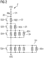
- Figure 2 shows a second embodiment of an electric circuit for trimming a resistance of a (fixed) resistor Rfix.
- Figure 2 illustrates how the structure of Figure 1 changes in the case that the LSB trimming resistor should be obtained as a parallel connection of bigger elements to comply with the minimum L/W rule.
- the embodiment of the electric circuit 2 shown in Figure 2 comprises a current path 20 comprising a plurality of sections 21, 22, 23, 24, ..., 2m.
- the current path 20 with the sections 21 to 20m is connected between a supply potential VDD and a reference potential VSS.
- the section 21 of the current path 20 comprises the (fixed) resistor Rfix to be trimmed.
- the subsequent section 22 that is connected in series to the section 21 of the current path 20 comprises a trimming resistor R22 that may be bypassed by a controllable switch S22.
- Each of the subsequent sections 23, 24, ..., 2m of the current path 20 comprises an increasing number of trimming resistors R22, R23, R24, ..., R2m per section, wherein the trimming resistors are connected in parallel in each of the sections 23, 24, ..., 2m.
- each of the sections 23, 24, ..., 2m of the current path 20 comprises a respective controllable switch S22, S23, S24, ..., S2m to bypass the parallel connection of the trimming resistors of the respective section of the current path 20.
- the respective controllable switch of each of the subsequent sections 22, 23, 24, ..., 2m of the current path 20 may be switched in a closed or open state.
- the LSB generation in the last section 2m of the current path 20 comprises 2 m-2 trimming resistors.
- a polyh resistor (1,200 Ohm per square) is considered to realistically generate 16 ⁇ A under a bandgap voltage. This requires a 75 kilo Ohm resistor, i.e. a little more than 60 squares.
- the second least significant digit would be made by connecting 16 trimming resistors in parallel, then 8 trimming resistors for the third least significant digit, then 4 trimming resistors, 2 trimming resistors and one trimming resistor to complete the trimming section, as shown in Figure 2 .
- this allows the possibility to tune the resistance of the resistor Rfix in a range as large as 24 kilo Ohm, i.e. +/- 16% from the nominal resistance value.
- the resistor Rfix will be trimmed from 63 kilo Ohm to 87 kilo Ohm in steps of 375 Ohm, and a total of 63 unit 10 square resistors will be used for trimming.
- the remaining untrimmed contribution, amounting to 63 kilo Ohm, is easily arranged with five series units plus four units in parallel. As a result, the trimming part of the electric trimming circuit would be seven times larger than the untrimmed portion.
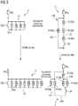
- Figure 3 shows two alternative embodiments of sections of a trimming circuit to generate the same variation of a resistance for a fixed resistor.
- Figure 3 shows, on the left side, the portion 24 of the electric circuit 2 for trimming the resistance of the resistor Rfix.
- the portion 24 comprises the four trimming resistors R24 having a resistance R.
- the trimming resistors may be bypassed by closing the controllable switch S24.
- the section 24 of the electric circuit 2 allows to vary the resistance of the resistor Rfix from 0 Ohm to R/4 Ohm depending on the switching status of the controllable switch S24.
- Figure 3 shows, on the right side, a section 120 of another embodiment of an electric circuit 3 for trimming the resistance of the resistor Rfix.
- the section 120 of the electric circuit 3 comprises a current branch 121 and a current branch 122 that may be connected in parallel by means of a controllable switch S3.
- the current branch 121 of the section 120 of the trimming circuit includes a single trimming resistor R120a having a resistance R.
- the current branch 122 includes a series connection of three trimming resistors R120b, R120c and R120d having a resistance R.
- the trimming resistors R120b, R120c and R120d can be electrically connected in parallel to the trimming resistor R120a, if the controllable switch S3 is turned in a conductive/closed state. In this way, the total resistance varies from 3 ⁇ 4 R to R.
- both embodiments fit the requirement to vary a resistance of a resistor Rfix by the same resistance step, where a resistance of 0 Ohm is not an option.
- the minimum resistance must be at least equal to 3 ⁇ 4 R.
- the same tuning capability is ensured. The difference in the total resistance can be easily corrected by making the untrimmed part consequently smaller, if the architecture of the trimming circuit 3 shown in the right side of Figure 3 is used.
- Figure 3 shows, in the bottom portion, on the left hand side a section 25 of the approach of the trimming circuit 2 and on the right hand side a section 150 of the approach of the trimming circuit 3 to arrange a smaller step of a resistance variation, i.e. a resistance variation of R/8.
- the number of trimming resistors R25 being connected in parallel in the section 25 of the trimming circuit 2 is doubled in comparison to the number of trimming resistors R24 of the section 24 to realize the resistance variation of R/8.
- the section 25 of the trimming circuit 2 comprises 8 trimming resistors.
- the 8 parallel connected trimming resistors R25 may be bypassed by a controllable switch S25.
- any single trimming resistor in the current branches 121 and 122 is replaced by two trimming resistors in parallel, while the series of two trimming resistors in the current branch 122 is replaced by only one trimming resistor.
- the trimming resistor R120a is replaced by the two trimming resistors R150a and R150b connected in parallel in the current branch 151 of the section 150 of the trimming circuit 3.
- the series connection of the two trimming resistors R120c and R120d of the section 120 of the trimming circuit 3 is replaced by a single trimming resistor R150e.
- the single trimming resistor R120b is replaced by the two trimming resistors R150c and R150d being connected in parallel in the current branch 152 of the section 150 of the trimming circuit 3.
- the controllable switch S3 of the section 120 of the trimming circuit 3 arranged in the current branch 122 remains unchanged and corresponds to the controllable switch S4 included in the current branch 152 of the section 150 of the trimming circuit 3.
- the section 25 of the trimming circuit 2 and the section 150 of the trimming circuit 3 are compared, it can be realized that the number of trimming resistors in the section 150 of the trimming circuit 3 is only increased by one, whereas the number of trimming resistors in the section 25 is doubled in comparison to the section 24 of the trimming circuit 2.
- the architecture of the trimming circuit 3 using the section 150 only uses five trimming resistors instead of eight trimming resistors in the section 25 of the trimming circuit 2.
- the configuration of the trimming circuit 3 enables to save area on a supporting substrate, for example a printed circuit board, of the trimming circuit.
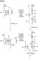
- Figure 4 generalizes the concept how the (N+1)th trimming section is obtained from the (N)th one for both approaches of the trimming circuits 2 and 3 shown in Figure 3 .
- Figure 4 illustrates the two alternative embodiments of respective sections of the trimming circuits 2 and 3 to generate the resistance variation with a step size of 1/2 N+1 starting from the 1/2 N step of resistance variation with M being a positive integer.
- Section 50 of the circuit approach 3 on the top right side of Figure 4 is another way to make a 1/2 N step of resistance change if compared to the structure 40 shown on the top left side of Figure 4 .
- both sections 40 and 50 use the same number of trimming resistors.
- the section 40 of the trimming circuit approach 2 shown on the left side of the top portion of Figure 4 uses 2 N parallel trimming resistors 30 which can be bypassed by a controllable switch S40.
- the section 50 of the other trimming circuit approach 3 shown on the right side of the top portion of Figure 4 uses one trimming resistor 53a in a current branch 51 and a series connection of 2 N -1 trimming resistors 53a, 53b, ..., 53n in a second current branch 52 that can be electrically connected in parallel to the current branch 51 by a controllable switch S50. If the switchable series of 2 N -1 similar trimming resistors 53b, 53c, ..., 53n is put in parallel to the single trimming resistor 53a, the generation of a R/2 N wide trimming step is obtained, changing the resistance from R to R ⁇ 1 ⁇ 1 / 2 N .
- the resistances in both current paths 51 and 52 are halved. That means that the single resistor 53a in the current branch 51 is replaced by a parallel connection of two trimming resistors 73a and 73b in the current branch 71. Furthermore, the series connection of the trimming resistors 53b, 53c, ..., 53n in the current branch 52 is replaced by a series connection of 2 N-1 -1 trimming resistors in the current branch 72 and a parallel connection of two trimming resistors 73c and 73d.
- the section 70 of the trimming circuit 3 comprises a controllable switch S70 that is configured to connect the current branches 71 and 72 electrically in parallel.
- the 1/2 N+1 step of resistance change is obtained with 3 + 2 N-1 trimming resistors, if the embodiment of the trimming circuit 3 is used.
- making the impedance halved using the approach of the trimming circuit 3 means to halve the number of trimming resistors connected in series in the current branch 72, not doubling them as shown for the configuration of the section 60 of the trimming circuit 2.
- the switchable path 52 including an odd number of trimming resistors the next LSB generation according to the scheme of the trimming circuit 3 requires 3 + 2 N-1 trimming resistors in total instead of 2 N+1 trimming resistors for the respective section of the trimming circuit 2. Large area savings follows, especially for large values of N.
- the table below shows the trimming step size (1/2 N+1 ) of the resistance change and the number of trimming resistors used in the last sections of the trimming circuits 2 and 3.
- N being an integer with N ⁇ 1
- the number of trimming resistors in the last section of the current path of the trimming circuit 2 according to the embodiment 2 results in 2 N+1
- number of trimming resistors in the last section of the current path of the trimming circuit 2 according to the embodiment 3 results in 3 + 2 N-1 .
- Trimming step size N Number of trimming resistors in last section of current path of embodiment 2 of trimming circuit Numbers of trimming resistors in last section of current path of embodiment 3 of trimming circuit 1/4 1 4 4 1/8 2 8 5 1/16 3 16 7 1/32 4 32 11 1/64 5 64 19
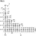
- Figures 5 and 6 respectively show an example for the trimming circuit 2 and 3 of the different approaches.
- Figure 5 shows an embodiment of an electric circuit 2 for trimming a resistance of a resistor Rfix using the approach illustrated on the left side of Figure 4 .
- Figure 6 shows an electric circuit 3 for trimming a resistance of a resistor Rfix using the approach shown on the right side of Figure 4 .
- FIG 5 shows an embodiment of a 5-bit trimming approach of an electric circuit for trimming a resistance of the resistor Rfix.
- the configuration of the electric circuit 2 is based on the approach illustrated in Figure 2 or in the left portions of Figures 3 and 4 .
- the electric circuit 2 comprises a current path 20 including a plurality of sections 21, 22, 23, 24, 25 and 26 being connected in series between a supply potential VDD and a reference potential VSS.
- the section 21 of the current path 20 comprises the (fixed) resistor Rfix of which its resistance is trimmed by the trimming sections 22, 23, 24, 25 and 26.
- the trimming section 22 comprises a single resistor R22 that can be bypassed by a controllable switch S1.
- the subsequent trimming section 23 comprises the two parallel connected resistors R23 that may be bypassed by the controllable switch S2.
- the trimming circuit 2 further comprises the trimming section 24 including the four parallel connected trimming resistors R24 that may be bypassed by a controllable switch S3.
- the subsequently arranged trimming section 25 comprises eight trimming resistors R25 that can be bypassed by the controllable switch S4.
- the last trimming section 26 comprises sixteen trimming resistors R26 that can be bypassed by the controllable switch S5.
- the controllable switches S1, ..., S5 may be controlled to be turned in a closed or open state by means of a controller circuit not shown in Figure 5 .
- the (fixed) resistor Rfix can be trimmed to different resistances.
- the embodiment of the electric trimming circuit 2 shown in Figure 5 to realize the 5-bit trimming approach includes 31 trimming resistors in the several trimming sections 22 to 26 having the same resistance R.
- Figure 5 illustrates that a trimming section is doubled with parallel resistors in the subsequent trimming section to generate the next lower LSB.
- Each trimming section can be bypassed by the corresponding controllable switch S1, ..., S5 to modulate the value of the (fixed) resistor Rfix.
- Figure 5 clearly shows that the area increase for the trimming circuit 2 is exponential with the number of bits. K bits require 2 K -1 trimming resistors.
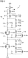
- FIG. 6 shows an embodiment of an electric circuit 3 for trimming a resistance of a (fixed) resistor Rfix.
- the circuit 3 comprises a current path 100 including a section 110 and a section 120.
- the section 110 and the section 120 are connected in series in the current path 10.
- the section 110 includes the fixed resistor Rfix to be trimmed.
- the section 120 of the current path 100 includes a current branch 121 and a current branch 122.
- the current branch 121 of the trimming section 120 of the current path 100 includes at least a trimming resistor R120a.
- the current branch 122 of the trimming section 120 of the current path 100 includes a series connection of a controllable switch S3 and at least a trimming resistor R120b, a trimming resistor R120c and a trimming resistor R120d.
- the current branch 122 comprises at least three trimming resistors.
- the controllable switch S3 of the current branch 122 of the trimming section 120 of the current path 100 is configured to connect the current path 122, i.e. the trimming resistors R120b, R120c and R120d in parallel to the current path 121, i.e. the trimming resistor R120a, when the controllable switch S3 is operated in the closed state.
- the current path 100 further comprises a trimming section 130 being connected in series to the section 110 of the current path 100.
- the trimming section 130 of the current path 100 includes a trimming resistor R130 and a controllable switch S1.
- the controllable switch S1 is configured to connect the trimming resistor R130 in series to the section 110 of the current path 100, i.e. to the (fixed) resistor Rfix, when the controllable switch S1 is turned in an open state.
- the controllable switch S1 is further configured to bypass the trimming resistor R130 so that the section 110 of the current path 100, i.e. the (fixed) resistor Rfix is connected to the trimming section 120 of the current path 100 by/via the controllable switch S1, when the controllable switch S1 of the trimming section 130 of the current path 100 is turned in the closed state.
- the current path 100 further comprises a trimming section 140 being connected in series between the trimming section 130 and the trimming section 120 of the current path 100.
- the trimming section 140 includes a trimming resistor R140a and a trimming resistor R140b being connected in parallel.
- the trimming section 140 further comprises a controllable switch S2 being configured to be operated in a closed and an open state.
- the controllable switch S2 of the trimming section 140 of the current path 100 is configured to connect the parallel connection of the trimming resistors R140a and R140b in series between the trimming section 120 and the trimming section 130 of the current path 100, when the controllable switch S2 is operated in the open state.
- the controllable switch S2 of the trimming section 140 is further configured to bypass the parallel connection of the trimming resistors R140a and R140b so that the trimming section 130 is connected to the trimming section 120 of the current path by/via the controllable switch S2, when the controllable switch S2 is operated in the closed state.
- the current path 100 includes at least one other trimming section being connected in series to the first, the second, the third and the fourth trimming section 110, 120, 130, 140 of the current path 100.
- the current path 100 comprises the trimming section 150 and the additional trimming section 150' that are both connected in series to the first, the second, the third and the fourth trimming section 110, 120, 130, 140 of the current path 100.
- the trimming section 150 of the current path 100 includes a current branch 151 and a current branch 152.
- the current branch 151 of the trimming section 150 includes a trimming resistor R150a and a trimming resistor 150b being connected in parallel.
- the current branch 152 includes a trimming resistor R150c and a trimming resistor R150d being connected in parallel.
- the current branch 152 of the trimming section 150 of the current path 100 further includes at least one trimming resistor R150e being connected in series to the parallel connection of the trimming resistors R150c and R150d.
- the current branch 152 of the trimming section 150 of the current path 100 further includes a controllable switch S4.
- the controllable switch S4 is connected in series to the parallel connection of the trimming resistors R150c and R150d.
- the controllable switch S4 of the trimming section 150 is configured to connect the current branch 152 in parallel to the current branch 151, when the controllable switch S4 of the trimming section 150 is operated in the closed state.
- the controllable switch S4 is further configured to isolate/separate the current branch 152 from the current branch 151, when the controllable switch S4 is operated in the open state.
- the current path 100 comprises the additional trimming section 150' being connected in series to the previous trimming sections 110, 120, 130, 140 and 150.
- the trimming section 150' includes a current branch 151' and a current branch 152' being connected in parallel.
- the current branch 151' comprises a trimming resistor R150'a and a trimming resistor R150'b being connected in parallel in the current branch 151'.
- the current branch 152' includes a trimming resistor R150'c and a trimming resistor R150'd being connected in parallel.
- the current branch 152' includes three trimming resistors R150'e, R150'f and R150'g being connected in series to the parallel connection of the trimming resistors R150'c and R150'd.
- the current branch 152' further comprises a controllable switch S5 that is connected in series to the parallel connection of the trimming resistors R150'c and R150'd.
- the controllable switch S5 of the current branch 152' is configured to connect the current branch 152' in parallel to the current branch 151', when the controllable switch S5 is operated in the closed state.
- the controllable switch S5 is further configured to isolate/separate the current branches 151' and 152' and thus the parallel connection of the trimming resistors R150'c and R150'd of the current branch 152' from the current branch 151', when the controllable switch S5 is operated in the open state.
- the at least one other trimming section comprises the trimming section 150 and the trimming section 150'.
- Each of the current branches 152 and 152' includes an odd number of trimming resistors R150e or R150'e, R150'f and R150'g being connected in series to the parallel connection of the trimming resistors R150c, R150d or R150'c, R150'd.
- Each of the trimming resistors in the trimming sections 130, ..., 150, 150' can have the same resistance R.
- each of the controllable switches S1 to S5 can be switched in the open or closed state.
- the approaches of the electric trimming circuits 2 and 3 are compared, it can be asserted that, as any bit adds an offset. This means that the untrimmed part of the resistance is smaller if the approach of the electric trimming circuit 3 is used. This saves additional area.
- the controllable switches of the sections of the electric trimming circuit 3 are always connected in series to several trimming resistors, unlike in the approach of the trimming circuit 2. In this way, the on-resistance of the controllable switches is less relevant in determining the trimming accuracy. This makes another remarkable saving of area.
- the switch size of the controllable switches in the trimming sections of the trimming circuit 3 is smaller in comparison to the switch size of the controllable switches in the trimming sections of the trimming circuit 2.
- INL integrated non-linearity
- DNL differential non-linearity
Abstract
Description
- The disclosure relates to an electric circuit for trimming a resistance of a resistor in a current path. The disclosure further relates to a method for trimming a resistance of the resistor.
- Integrated resistors usually undergo a large spread versus process. Starting from a typical value, a variation of a resistance of a resistor as large as +/- 20% can usually be observed in different production lots. One of the most typical applications which is affected by this problem is a voltage-to-current converter by means of which a precise reference current is obtained on a chip by loading a bandgap voltage with a resistor. Since the bandgap voltage is usually trimmed as well, the large resistor spread creates a 20% inaccuracy of the generated current.
- To simplify calculations, assuming a +/- 16% spread of the resistance of a resistor, if the accuracy target is 0.5%, the resistance of the resistor should be tuned from 84% to 116% of its nominal value in 6 bits. The two extreme values of the resistance range correspond to the trimming options to be selected in cases where the process provides a resistance of the resistor that is 16% bigger than the nominal resistance and 16% smaller than the nominal resistance, respectively. Remarkably, the resistance of a resistor does not need to be trimmed from a value of 0 Ohm to the highest possible value. The minimum value of the resistance is largely greater than 0 Ohm.
- There is a need to provide an electric circuit for trimming a resistance of a resistor with a high accuracy, wherein the trimming circuit avoids a large area consumption. Furthermore, there is a need to provide a method for trimming a resistance of a resistor with a high accuracy without wasting a large area for the electric circuit.
- An electric circuit for trimming a resistance of a resistor which does not consume a large area and allows to trim the resistance of the resistor with high accuracy is specified in
claim 1. - The circuit for trimming the resistance of the resistor comprises a current path including a first section and at least a second section, wherein the first and the at least one second section are connected in series in the current path. The first section of the current path includes the resistor to be trimmed.
- Depending on the accuracy/step size by which the (fixed) resistor of the first section of the current path is to be trimmed, the electric circuit may comprise several of the at least one second section in the current path. The at least one second section of the current path includes a first current branch and a second current branch being connected in parallel. The first current branch of the at least one fifth section of the current path includes a first and a second trimming resistor being connected in parallel.
- The second current branch of the at least one second section of the current path includes a third trimming resistor and a fourth trimming resistor being connected in parallel. The second current branch of the at least one second section of the current path includes at least one fifth trimming resistor being connected in series to the parallel connection of the third and the fourth trimming resistor. Furthermore, the second current branch of the at least one second section of the current path includes a controllable switch. The controllable switch of the at least one second section of the current path is connected in series to the parallel connection of the third and the fourth trimming resistor.
- The controllable switch of the at least one second section of the current path is configured to electrically connect the second current branch of the at least one second section of the current path, and thus the parallel connection of the third and the fourth trimming resistor, in parallel to the first current branch of the at least one second section of the current path, when the controllable switch of the at least one second section of the current path is operated in the closed state. The controllable switch of the at least one second section of the current path is further configured to isolate the second current branch of the at least one second section of the current path, and thus the parallel connection of the third and the fourth trimming resistor, from the first current branch of the at least one second section of the current path, when the controllable switch of the at least one second section of the current path is operated in the open state.
- The current path may further comprise a third section being connected in series to the first section of the current path. The third section of the current path may comprise a sixth trimming resistor and a controllable switch. The controllable switch of the third section of the current path is configured to electrically connect the sixth trimming resistor in series to the first section of the current path and further in series to the at least one second section of the current path, when the controllable switch is turned in an open state. In the closed state, the controllable switch of the third section of the current path is configured to bypass the sixth trimming resistor so that the first section of the current path is connected to the at least one second section of the current path via the closed controllable switch of the third section of the current path.
- The current path may comprise a fourth section being connected in series to the third section and the at least one second section of the current path. The fourth section of the current path may comprise a seventh trimming resistor and an eighth trimming resistor being connected in parallel. The fourth section of the current path may comprise a controllable switch that is configured to connect the parallel connection of the seventh and the eighth trimming resistor in series between the second section and the third section of the current path, when the controllable switch is operated in an open state. The controllable switch of the fourth section of the current path is further configured to bypass the parallel connection of the seventh and the eighth trimming resistor so that the third section of the current path is electrically connected to the at least one second section of the current path via the controllable switch of the fourth section of the current path, when the controllable switch of the fourth section of the current path is operated in the closed state.
- The current path includes a fifth section comprising a first current branch and a second current branch. The first current branch of the fifth section of the current path includes at least a ninth trimming resistor. The second current branch of the fifth section of the current path includes a series connection of a controllable switch and at least a tenth and an eleventh and a twelfth trimming resistor. The controllable switch of the second current branch of the fifth section of the current path is configured to electrically connect the at least one tenth and eleventh and twelfth trimming resistor of the second current branch of the fifth section of the current path in parallel to the at least one ninth trimming resistor of the first current branch of the fifth section of the current path, when the controllable switch of the second current branch of the fifth section of the current path is operated in a closed state.
- A method for trimming a resistance of a resistor is specified in
claim 12. - According to the method, the resistance of the (fixed) resistor is trimmed by closing or opening at least one of the controllable switches of the at least one second, the third, the fourth and the fifth section of the current path in dependence on the sections provided in the current path and thus in dependence on the available trimming steps/sections.
- Additional features and advantages are set forth in the detailed description that follows and in part will be readily apparent to those skilled in the art from the description or recognized by practising the embodiments as described in the written description and claims hereof, as well as the appended drawings. It is to be understood that both the foregoing general description and the following detailed description are merely exemplary, and are intended to provide an overview or framework to understand the nature and character of the claims.
- The accompanying drawings are included to provide further understanding, and are incorporated in and constitute a part of the specification. The drawings illustrate one or more embodiments, and together with the detailed description serve to explain principles and operation of the various embodiments. As such, the disclosure will become more fully understood from the following detailed description, taken in conjunction with the accompanying figures in which
- Figure 1
- shows a first embodiment of an electric circuit for trimming a resistance of a resistor;
- Figure 2
- shows a second embodiment of an electric circuit for trimming a resistance of a resistor;
- Figure 3
- illustrates different approaches of sections of an electric circuit to provide the same resistance variation of a resistor;
- Figure 4
- illustrates generalized different approaches of sections of an electric circuit to provide the same resistance variation of a resistor;
- Figure 5
- shows a first embodiment of an electric circuit realizing a 5 bit trimming approach;
- Figure 6
- shows a second embodiment of an electric circuit for trimming a resistance of a resistor using a 5 bit trimming approach;
- Reference is now made in detail to various embodiments of the disclosure, examples of which are illustrated in the accompanying drawings. Whenever possible, the same or like reference numbers and symbols are used throughout the drawings to refer to the same or like parts. The drawings are not necessary to scale, and one skilled in the art will recognize where the drawings have been simplified to illustrate the key aspects of the disclosure. The claims as set forth below are incorporated into and constitute part of this detailed description.
-
Figure 1 shows a first embodiment of anelectric circuit 1 to trim a resistance of a fixed resistor Rfix. Theelectric circuit 1 comprises acurrent path 10 being connected between a supply potential VDD and a reference potential VSS. The current path comprises asection 11 comprising the (fixed) resistor Rfix. Theelectric circuit 1 may comprise a plurality ofsections current path 10 in dependence on the trimming accuracy or trimming step size of the resistance of the resistor Rfix. Each of the sections may comprise a respective controllable switch S12, S13, S14, ..., S1m and a respective trimming resistor R12, R13, R14, ..., R1m.Figure 1 shows the trimming resistors having a resistance R. Thesections current path 10 subsequent to thesection 11 of the current path that includes the resistor Rfix. - Each of the respective controllable switches S12, S13, S14, ..., S1m of the
sections current path 10 may be configured to connect the respective trimming resistor R12, R13, R14, ..., R1m of the sections of thecurrent path 10 in series to a previous and a subsequent section of thecurrent path 10, when the respective controllable switch is operated in the open state. In the closed state, each of the controllable switches of thecurrent section sections current path 10, the respective trimming resistor R12, R13, R14, ..., R1m of thesections - The electric circuit shown in
Figure 1 enables to trim the resistance of the (fixed) resistor Rfix by controlling the respective controllable switches S12, S13, S14, ..., S1m of thesections current path 10 in the closed or open state. It is clear that, still referring for the sake of simplicity, but not exclusively, to the range 84% to 116% of the resistance of the resistor Rfix with 6 trimming bits, the resistor Rfix is trimmed by using a respective trimming resistor in each of thesections - Using the respective controllable switches in each of the
sections current path 10, it is possible to bypass one single trimming resistor, i.e. the LSB, to adjust the resistance of the fixed resistor by 0.5%, to bypass two series trimming resistors to obtain a 1% adjustment (second least significant digit) of the resistance of the fixed resistor Rfix, to bypass four series trimming resistors for a 2% adjustment of the resistance of the resistor Rfix and so on until the total trimming range is covered. Any possible combination of the open/closed state of the controllable switches of therespective sections - The use of small unity trimming resistors ensures a large degree of matching, all the elements being equal, which is a key feature to develop a trimming system with small DNL (differential non-linearity) and INL (integral non-linearity).
- Anyhow, it is clear that 232 sections being connected in series in the
current path 10 would take a large area due to the large number of contacts and wiring. At the same time, the layout effort to provide all these connections should not be under-evaluated. - Unfortunately, these are not the only defects of such an approach. In fact, it has to be considered that a unity trimming resistor should be shaped with an L/W ratio (Length/Width ratio) that is quite large so that parasitic contributions of contacts and border effects are negligible. This becomes a serious problem if the total resistance of the resistor to be trimmed is not very large. Under the recommendation that a unity resistor should have at least five (or even ten) squares, this means that if the total resistance of the resistor Rfix is below 1,160 (or 2,320) squares, the less significant bits should be obtained with more trimming resistors in parallel in each of the sections of the current path, as shown in
Figure 2 . -
Figure 2 shows a second embodiment of an electric circuit for trimming a resistance of a (fixed) resistor Rfix.Figure 2 illustrates how the structure ofFigure 1 changes in the case that the LSB trimming resistor should be obtained as a parallel connection of bigger elements to comply with the minimum L/W rule. - The embodiment of the
electric circuit 2 shown inFigure 2 comprises acurrent path 20 comprising a plurality ofsections current path 20 with thesections 21 to 20m is connected between a supply potential VDD and a reference potential VSS. Thesection 21 of thecurrent path 20 comprises the (fixed) resistor Rfix to be trimmed. Thesubsequent section 22 that is connected in series to thesection 21 of thecurrent path 20 comprises a trimming resistor R22 that may be bypassed by a controllable switch S22. Each of thesubsequent sections current path 20 comprises an increasing number of trimming resistors R22, R23, R24, ..., R2m per section, wherein the trimming resistors are connected in parallel in each of thesections - Furthermore, each of the
sections current path 20 comprises a respective controllable switch S22, S23, S24, ..., S2m to bypass the parallel connection of the trimming resistors of the respective section of thecurrent path 20. In order to trim the (fixed) resistor Rfix in thesection 21 of thecurrent path 20, the respective controllable switch of each of thesubsequent sections current path 20 may be switched in a closed or open state. - As shown in
Figure 2 , the LSB generation in thelast section 2m of thecurrent path 20 comprises 2m-2 trimming resistors. This might lead to a significant waste of area. As an example, a polyh resistor (1,200 Ohm per square) is considered to realistically generate 16 µA under a bandgap voltage. This requires a 75 kilo Ohm resistor, i.e. a little more than 60 squares. An accuracy target of 0.5%, i.e. 375 Ohm, means that 1LSB should be made by 32 unity trimming resistors in parallel to comply with the 10 squares minimum rule for resistors. The second least significant digit would be made by connecting 16 trimming resistors in parallel, then 8 trimming resistors for the third least significant digit, then 4 trimming resistors, 2 trimming resistors and one trimming resistor to complete the trimming section, as shown inFigure 2 . In the end, this allows the possibility to tune the resistance of the resistor Rfix in a range as large as 24 kilo Ohm, i.e. +/- 16% from the nominal resistance value. - In the end, the resistor Rfix will be trimmed from 63 kilo Ohm to 87 kilo Ohm in steps of 375 Ohm, and a total of 63
unit 10 square resistors will be used for trimming. The remaining untrimmed contribution, amounting to 63 kilo Ohm, is easily arranged with five series units plus four units in parallel. As a result, the trimming part of the electric trimming circuit would be seven times larger than the untrimmed portion. - As explained above, in most applications the (fixed) resistor Rfix does not need to be trimmed from 0 Ohm. Regarding the approach of
Figure 2 , most of the area of the electric circuit for trimming the resistance of the resistor Rfix is lost to generate one LSB variation in the resistor value. -
Figure 3 shows two alternative embodiments of sections of a trimming circuit to generate the same variation of a resistance for a fixed resistor. -
Figure 3 shows, on the left side, theportion 24 of theelectric circuit 2 for trimming the resistance of the resistor Rfix. Theportion 24 comprises the four trimming resistors R24 having a resistance R. The trimming resistors may be bypassed by closing the controllable switch S24. Thesection 24 of theelectric circuit 2 allows to vary the resistance of the resistor Rfix from 0 Ohm to R/4 Ohm depending on the switching status of the controllable switch S24. -
Figure 3 shows, on the right side, asection 120 of another embodiment of anelectric circuit 3 for trimming the resistance of the resistor Rfix. This structure also enables to vary the resistance of the resistor Rfix by R/4. Thesection 120 of theelectric circuit 3 comprises acurrent branch 121 and acurrent branch 122 that may be connected in parallel by means of a controllable switch S3. Thecurrent branch 121 of thesection 120 of the trimming circuit includes a single trimming resistor R120a having a resistance R. Thecurrent branch 122 includes a series connection of three trimming resistors R120b, R120c and R120d having a resistance R. The trimming resistors R120b, R120c and R120d can be electrically connected in parallel to the trimming resistor R120a, if the controllable switch S3 is turned in a conductive/closed state. In this way, the total resistance varies from ¾ R to R. - If the
section 120 of thetrimming circuit 3 is compared with asection 24 it may be realized that the variation of the resistance in both cases is R/4. Hence, both embodiments fit the requirement to vary a resistance of a resistor Rfix by the same resistance step, where a resistance of 0 Ohm is not an option. Indeed, regarding the architecture of thetrimming circuit 3, the minimum resistance must be at least equal to ¾ R. Besides the difference that the total resistance is increased starting from ¾ R to R in the case that the architecture of the right side inFigure 3 is used, the same tuning capability is ensured. The difference in the total resistance can be easily corrected by making the untrimmed part consequently smaller, if the architecture of thetrimming circuit 3 shown in the right side ofFigure 3 is used. -
Figure 3 shows, in the bottom portion, on the left hand side asection 25 of the approach of thetrimming circuit 2 and on the right hand side asection 150 of the approach of thetrimming circuit 3 to arrange a smaller step of a resistance variation, i.e. a resistance variation of R/8. Starting from the twostructures Figure 3 to realize a resistance variation of R/4, it is sufficient to divide each of thesections - As concerns the approach of the
trimming circuit 2 on the left side ofFigure 3 , the number of trimming resistors R25 being connected in parallel in thesection 25 of thetrimming circuit 2 is doubled in comparison to the number of trimming resistors R24 of thesection 24 to realize the resistance variation of R/8. Instead of 4 parallel connected trimming resistors of thesection 24 of thetrimming circuit 2, thesection 25 of thetrimming circuit 2 comprises 8 trimming resistors. The 8 parallel connected trimming resistors R25 may be bypassed by a controllable switch S25. - If the
section 120 of thetrimming circuit 3 on the right side ofFigure 3 is divided by two to realize a change of the resistance of R/8, any single trimming resistor in thecurrent branches current branch 122 is replaced by only one trimming resistor. In particular, the trimming resistor R120a is replaced by the two trimming resistors R150a and R150b connected in parallel in thecurrent branch 151 of thesection 150 of thetrimming circuit 3. The series connection of the two trimming resistors R120c and R120d of thesection 120 of thetrimming circuit 3 is replaced by a single trimming resistor R150e. The single trimming resistor R120b is replaced by the two trimming resistors R150c and R150d being connected in parallel in thecurrent branch 152 of thesection 150 of thetrimming circuit 3. The controllable switch S3 of thesection 120 of thetrimming circuit 3 arranged in thecurrent branch 122 remains unchanged and corresponds to the controllable switch S4 included in thecurrent branch 152 of thesection 150 of thetrimming circuit 3. - If the
section 25 of thetrimming circuit 2 and thesection 150 of thetrimming circuit 3 are compared, it can be realized that the number of trimming resistors in thesection 150 of thetrimming circuit 3 is only increased by one, whereas the number of trimming resistors in thesection 25 is doubled in comparison to thesection 24 of thetrimming circuit 2. In particular, to realize the resistance variation of R/8, the architecture of thetrimming circuit 3 using thesection 150 only uses five trimming resistors instead of eight trimming resistors in thesection 25 of thetrimming circuit 2. The configuration of thetrimming circuit 3 enables to save area on a supporting substrate, for example a printed circuit board, of the trimming circuit. -
Figure 4 generalizes the concept how the (N+1)th trimming section is obtained from the (N)th one for both approaches of the trimmingcircuits Figure 3 . In particular,Figure 4 illustrates the two alternative embodiments of respective sections of the trimmingcircuits -
Section 50 of thecircuit approach 3 on the top right side ofFigure 4 is another way to make a 1/2N step of resistance change if compared to thestructure 40 shown on the top left side ofFigure 4 . Starting from the 1/2N step of resistance change and consideringsection 40 of thecircuit approach 2 on the left side andsection 50 of thecircuit approach 3 on the right side of the top portion ofFigure 4 , bothsections section 40 of thetrimming circuit approach 2 shown on the left side of the top portion ofFigure 4 uses 2Nparallel trimming resistors 30 which can be bypassed by a controllable switch S40. Thesection 50 of the othertrimming circuit approach 3 shown on the right side of the top portion ofFigure 4 uses onetrimming resistor 53a in acurrent branch 51 and a series connection of 2N-1trimming resistors current branch 52 that can be electrically connected in parallel to thecurrent branch 51 by a controllable switch S50. If the switchable series of 2N-1similar trimming resistors single trimming resistor 53a, the generation of a R/2N wide trimming step is obtained, changing the resistance from R to
- Considering the starting blocks 40 and 50: Making half of these
blocks respective section 60 of thetrimming circuit 2 is illustrated in the bottom portion ofFigure 4 on the left hand side, and therespective section 70 of thetrimming circuit 3 is illustrated in the bottom portion ofFigure 4 on the right hand side. For the approach of thetrimming circuit 2 halving a given number of theparallel trimming resistors 30 means to double their number, as all elements/trimming resistors are still kept in parallel. This leads to 2 x 2N = 2N+1trimming resistors 31 for thesection 60 of thetrimming circuit 2. - In order to halve the change of the resistance of the
section 50 of thetrimming circuit 3 from 1/2N to 1/2N+1, the resistances in bothcurrent paths single resistor 53a in thecurrent branch 51 is replaced by a parallel connection of two trimmingresistors current branch 71. Furthermore, the series connection of the trimmingresistors current branch 52 is replaced by a series connection of 2N-1-1 trimming resistors in thecurrent branch 72 and a parallel connection of two trimmingresistors section 50 of thetrimming circuit 3, thesection 70 of thetrimming circuit 3 comprises a controllable switch S70 that is configured to connect thecurrent branches trimming circuit 3 is used. - When compared to the
section 60, making the impedance halved using the approach of thetrimming circuit 3 means to halve the number of trimming resistors connected in series in thecurrent branch 72, not doubling them as shown for the configuration of thesection 60 of thetrimming circuit 2. Being theswitchable path 52 including an odd number of trimming resistors, the next LSB generation according to the scheme of thetrimming circuit 3 requires 3 + 2N-1 trimming resistors in total instead of 2N+1 trimming resistors for the respective section of thetrimming circuit 2. Large area savings follows, especially for large values of N. - The table below shows the trimming step size (1/2N+1) of the resistance change and the number of trimming resistors used in the last sections of the trimming
circuits trimming circuit 2 according to theembodiment 2 results in 2N+1, and number of trimming resistors in the last section of the current path of thetrimming circuit 2 according to theembodiment 3 results in 3 + 2N-1.Trimming step size N Number of trimming resistors in last section of current path of embodiment 2 of trimming circuitNumbers of trimming resistors in last section of current path of embodiment 3 of trimmingcircuit 1/4 1 4 4 1/8 2 8 5 1/16 3 16 7 1/32 4 32 11 1/64 5 64 19 -
Figures 5 and6 respectively show an example for thetrimming circuit Figure 5 shows an embodiment of anelectric circuit 2 for trimming a resistance of a resistor Rfix using the approach illustrated on the left side ofFigure 4 .Figure 6 shows anelectric circuit 3 for trimming a resistance of a resistor Rfix using the approach shown on the right side ofFigure 4 . -
Figure 5 shows an embodiment of a 5-bit trimming approach of an electric circuit for trimming a resistance of the resistor Rfix. The configuration of theelectric circuit 2 is based on the approach illustrated inFigure 2 or in the left portions ofFigures 3 and4 . Theelectric circuit 2 comprises acurrent path 20 including a plurality ofsections section 21 of thecurrent path 20 comprises the (fixed) resistor Rfix of which its resistance is trimmed by the trimmingsections trimming section 22 comprises a single resistor R22 that can be bypassed by a controllable switch S1. Thesubsequent trimming section 23 comprises the two parallel connected resistors R23 that may be bypassed by the controllable switch S2. Thetrimming circuit 2 further comprises thetrimming section 24 including the four parallel connected trimming resistors R24 that may be bypassed by a controllable switch S3. The subsequently arranged trimmingsection 25 comprises eight trimming resistors R25 that can be bypassed by the controllable switch S4. Thelast trimming section 26 comprises sixteen trimming resistors R26 that can be bypassed by the controllable switch S5. - The controllable switches S1, ..., S5 may be controlled to be turned in a closed or open state by means of a controller circuit not shown in
Figure 5 . In dependence on the state of the controllable switches S1, ..., S5 the (fixed) resistor Rfix can be trimmed to different resistances. - The embodiment of the
electric trimming circuit 2 shown inFigure 5 to realize the 5-bit trimming approach includes 31 trimming resistors in theseveral trimming sections 22 to 26 having the same resistance R.Figure 5 illustrates that a trimming section is doubled with parallel resistors in the subsequent trimming section to generate the next lower LSB. Each trimming section can be bypassed by the corresponding controllable switch S1, ..., S5 to modulate the value of the (fixed) resistor Rfix.Figure 5 clearly shows that the area increase for thetrimming circuit 2 is exponential with the number of bits. K bits require 2K-1 trimming resistors. -
Figure 6 shows an embodiment of anelectric circuit 3 for trimming a resistance of a (fixed) resistor Rfix. Thecircuit 3 comprises acurrent path 100 including asection 110 and asection 120. Thesection 110 and thesection 120 are connected in series in thecurrent path 10. Thesection 110 includes the fixed resistor Rfix to be trimmed. Thesection 120 of thecurrent path 100 includes acurrent branch 121 and acurrent branch 122. Thecurrent branch 121 of thetrimming section 120 of thecurrent path 100 includes at least a trimming resistor R120a. Thecurrent branch 122 of thetrimming section 120 of thecurrent path 100 includes a series connection of a controllable switch S3 and at least a trimming resistor R120b, a trimming resistor R120c and a trimming resistor R120d. Thecurrent branch 122 comprises at least three trimming resistors. The controllable switch S3 of thecurrent branch 122 of thetrimming section 120 of thecurrent path 100 is configured to connect thecurrent path 122, i.e. the trimming resistors R120b, R120c and R120d in parallel to thecurrent path 121, i.e. the trimming resistor R120a, when the controllable switch S3 is operated in the closed state. - The
current path 100 further comprises atrimming section 130 being connected in series to thesection 110 of thecurrent path 100. Thetrimming section 130 of thecurrent path 100 includes a trimming resistor R130 and a controllable switch S1. The controllable switch S1 is configured to connect the trimming resistor R130 in series to thesection 110 of thecurrent path 100, i.e. to the (fixed) resistor Rfix, when the controllable switch S1 is turned in an open state. The controllable switch S1 is further configured to bypass the trimming resistor R130 so that thesection 110 of thecurrent path 100, i.e. the (fixed) resistor Rfix is connected to thetrimming section 120 of thecurrent path 100 by/via the controllable switch S1, when the controllable switch S1 of thetrimming section 130 of thecurrent path 100 is turned in the closed state. - The
current path 100 further comprises atrimming section 140 being connected in series between the trimmingsection 130 and thetrimming section 120 of thecurrent path 100. Thetrimming section 140 includes a trimming resistor R140a and a trimming resistor R140b being connected in parallel. Thetrimming section 140 further comprises a controllable switch S2 being configured to be operated in a closed and an open state. The controllable switch S2 of thetrimming section 140 of thecurrent path 100 is configured to connect the parallel connection of the trimming resistors R140a and R140b in series between the trimmingsection 120 and thetrimming section 130 of thecurrent path 100, when the controllable switch S2 is operated in the open state. The controllable switch S2 of thetrimming section 140 is further configured to bypass the parallel connection of the trimming resistors R140a and R140b so that thetrimming section 130 is connected to thetrimming section 120 of the current path by/via the controllable switch S2, when the controllable switch S2 is operated in the closed state. - The
current path 100 includes at least one other trimming section being connected in series to the first, the second, the third and thefourth trimming section current path 100. According to the exemplified embodiment of thecurrent path 100 of theelectric circuit 3, thecurrent path 100 comprises thetrimming section 150 and the additional trimming section 150' that are both connected in series to the first, the second, the third and thefourth trimming section current path 100. - The
trimming section 150 of thecurrent path 100 includes acurrent branch 151 and acurrent branch 152. Thecurrent branch 151 of thetrimming section 150 includes a trimming resistor R150a and a trimming resistor 150b being connected in parallel. Thecurrent branch 152 includes a trimming resistor R150c and a trimming resistor R150d being connected in parallel. Thecurrent branch 152 of thetrimming section 150 of thecurrent path 100 further includes at least one trimming resistor R150e being connected in series to the parallel connection of the trimming resistors R150c and R150d. - The
current branch 152 of thetrimming section 150 of thecurrent path 100 further includes a controllable switch S4. The controllable switch S4 is connected in series to the parallel connection of the trimming resistors R150c and R150d. The controllable switch S4 of thetrimming section 150 is configured to connect thecurrent branch 152 in parallel to thecurrent branch 151, when the controllable switch S4 of thetrimming section 150 is operated in the closed state. The controllable switch S4 is further configured to isolate/separate thecurrent branch 152 from thecurrent branch 151, when the controllable switch S4 is operated in the open state. - According to the 5-bit trimming scheme shown in
Figure 6 , thecurrent path 100 comprises the additional trimming section 150' being connected in series to theprevious trimming sections - The current branch 152' further comprises a controllable switch S5 that is connected in series to the parallel connection of the trimming resistors R150'c and R150'd. The controllable switch S5 of the current branch 152' is configured to connect the current branch 152' in parallel to the current branch 151', when the controllable switch S5 is operated in the closed state. The controllable switch S5 is further configured to isolate/separate the current branches 151' and 152' and thus the parallel connection of the trimming resistors R150'c and R150'd of the current branch 152' from the current branch 151', when the controllable switch S5 is operated in the open state.
- As illustrated in
Figure 6 , the at least one other trimming section comprises thetrimming section 150 and the trimming section 150'. Each of thecurrent branches 152 and 152' includes an odd number of trimming resistors R150e or R150'e, R150'f and R150'g being connected in series to the parallel connection of the trimming resistors R150c, R150d or R150'c, R150'd. Each of the trimming resistors in the trimmingsections 130, ..., 150, 150' can have the same resistance R. In order to vary/trim the value of the (fixed) resistor Rfix, each of the controllable switches S1 to S5 can be switched in the open or closed state. - As is apparent from the embodiment of the
electric circuit 3 ofFigure 6 in comparison to theelectric circuit 2 shown inFigure 5 , increasing the number of bits makes the approach of theelectric trimming circuit 3 increasingly convenient. For a 5-bit trimming scheme, only 19 trimming resistors are used for theelectric trimming circuit 3 ofFigure 6 instead of 31 trimming resistors used for the approach of theelectric trimming circuit 2 shown inFigure 5 . The trend would converge to four times less area for a large number of trimming bits. For a very large number of trimming bits K, the trend would be frustrated by the fact that the total resistance would increase to far beyond the target limits. Any additional K-th bit introduces an offset equal to R/2 - 1/2K over the minimum achievable resistance. Hence, the number K of the bits is limited by the relationship K x R/2 < Rmax. Anyhow this constraint is fully acceptable in any practical implementation. - If the approaches of the
electric trimming circuits electric trimming circuit 3 is used. This saves additional area. Moreover, it has to be emphasized that the controllable switches of the sections of theelectric trimming circuit 3 are always connected in series to several trimming resistors, unlike in the approach of thetrimming circuit 2. In this way, the on-resistance of the controllable switches is less relevant in determining the trimming accuracy. This makes another remarkable saving of area. Moreover, the switch size of the controllable switches in the trimming sections of thetrimming circuit 3 is smaller in comparison to the switch size of the controllable switches in the trimming sections of thetrimming circuit 2. In the end, despite the reduced area, INL (integral non-linearity) and DNL (differential non-linearity) are not frustrated in the approach of theelectric trimming circuit 3 because the area saving is achieved in the generation of the LSB, where a large percentage error is easily tolerated. -
- 1, 2, 3
- embodiments of electric trimming circuits
- 10
- current path
- 11, ..., 1m
- section of current path
- 20
- current path
- 21, ..., 2m
- sections of current path
- 30
- trimming resistor
- 40, 50, 60, 70
- section of current path
- 100
- current path
- 110, ..., 150'
- section of current path
- S
- controllable switch
- Rfix
- (fixed) resistor
Claims (15)
- An electric circuit for trimming a resistance of a resistor, comprising:- a current path (100) including a first section (110) and at least a second section (150), wherein the first and the at least one second section (110, 150) are connected in series in the current path (100),- wherein the first section (110) of the current path includes the resistor (Rfix) to be trimmed,- wherein the at least one second section (150) of the current path (100) includes a first current branch (151) and a second current branch (152),- wherein the first current branch (151) of the at least one second section (150) of the current path (100) includes a first trimming resistor (R150a) and a second trimming resistor (R150b) being connected in parallel,- wherein the second current branch (152) of the at least one second section (150) of the current path (100) includes a third trimming resistor (R150c) and a fourth trimming resistor (R150d) being connected in parallel.
- The electric circuit of claim 1,
wherein the second current branch (152) of the at least one second section (150) of the current path (100) includes at least one fifth trimming resistor (R150e) being connected in series to the parallel connection of the third and the fourth trimming resistor (R150c, R150d). - The electric circuit of claim 2,
wherein the second current branch (152) of the at least one second section (150) of the current path (100) includes an odd number of the at least one fifth trimming resistor (R150e) being connected in series to the parallel connection of the third and the fourth trimming resistor (R150c, R150d). - The electric circuit of claims 1 to 3,
wherein the second current branch (152) of the at least one second section (150) of the current path (100) includes a controllable switch (S4). - The electric circuit of claim 4,
wherein the controllable switch (S4) of the second current branch (152) of the at least one second section (150) of the current path (100) is connected in series to the parallel connection of the third and the fourth trimming resistor (R150c, R150d). - The electric circuit of claims 4 or 5,- wherein the controllable switch (S4) of the second current branch (152) of the at least one second section (150) of the current path (100) is configured to electrically connect the second current branch (152) of the at least one second section (150) of the current path (100) in parallel to the first current branch (151) of the at least one second section (150) of the current path (100), when the controllable switch (S4) of the second current branch (152) of the at least one second section (150) of the current path (100) is operated in the closed state,- wherein the controllable switch (S4) of the second current branch (152) of the at least one second section (150) of the current path (100) is configured to isolate the parallel connection of the third and the fourth trimming resistor (R150c, R150d) from the first current branch (151) of the at least one second section (150) of the current path (100), when the controllable switch (S4) of the second current branch (152) of the at least one second section (150) of the current path (100) is operated in the open state.
- The electric circuit of claim 1,- wherein the current path (100) comprises a third section (130) being connected in series to the first section (110) of the current path (100),- wherein the third section (130) of the current path (100) includes a sixth trimming resistor (R130) and a controllable switch (S1),- wherein the controllable switch (S1) of the third section (130) of the current path (100) is configured to connect the sixth trimming resistor (R130) in series to the first section (110) and the at least one second section (150) of the current path, when the controllable switch (S1) of the third section (130) of the current path (100) is turned in an open state,- wherein the controllable switch (S1) of the third section (130) of the current path (100) is configured to bypass the sixth trimming resistor (R130) so that the first section (110) of the current path (100) is electrically connected to the at least one second section (150) of the current path (100) via the controllable switch (S1) of the third section (130) of the current path, when the controllable switch (S1) of the third section (130) of the current path is operated in the closed state.
- The electric circuit of claim 7,- wherein the current path (100) comprises a fourth section (140) being connected in series to the third section (130) and the at least one second section (150) of the current path,- wherein the fourth section (140) of the current path (100) includes a seventh trimming resistor (R140a) and an eighth trimming resistor (R140b) being connected in parallel,- wherein the fourth section (140) of the current path (100) includes a controllable switch (S2) being configured to be operated in a closed and an open state.
- The electric circuit of claim 8,- wherein the controllable switch (S2) of the fourth section (140) of the current path (100) is configured to electrically connect the parallel connection of the seventh and the eighth trimming resistor (R140a, R140b) in series to the at least one second section (150) and the third section (130) of the current path, when the controllable switch (S2) of the fourth section (140) of the current path (100) is operated in the open state,- wherein the controllable switch (S2) of the fourth section (140) of the current path (100) is configured to bypass the parallel connection of the seventh and the eighth trimming resistor (R140a, R140b) so that the third section (130) of the current path is electrically connected to the at least one second section (150) of the current path via the controllable switch (S2) of the fourth section (140) of the current path, when the controllable switch (S2) of the fourth section (140) of the current path (100) is operated in the closed state.
- The electric circuit of claims 3 or 4,- wherein the current path (100) includes a fifth section (120) being connected in series to the first section (110), the at least one second section (150), the third section (130) and the fourth section (140) of the current path (100),- wherein the fifth section (120) of the current path includes a first current branch (121) and a second current branch (122),- wherein the first current branch (121) of the fifth section (120) of the current path (100) includes at least a ninth trimming resistor (R120a),- wherein the second current branch (122) of the fifth section (120) of the current path (100) includes a series connection of a controllable switch (S3) and at least a tenth and an eleventh and a twelfth trimming resistor (R120b, R120c, R120d),- wherein the controllable switch (S3) of the second current branch (122) of the second section (120) of the current path (100) is configured to electrically connect the at least one tenth and eleventh and twelfth trimming resistor (R120b, R120c, R120d) of the second current branch (122) of the second section (120) of the current path (100) in parallel to the at least one ninth trimming resistor (R120a) of the first current branch (121) of the second section (120) of the current path (100), when the controllable switch (S3) of the second current branch (122) of the second section (120) of the current path is operated in a closed state.
- The electric circuit of claims 9 or 10,
wherein the trimming resistors (R150a, ..., R150e) of the at least one second section (150), the trimming resistor (R130) of the third section (130), the trimming resistors (R140a, R140b) of the fourth section (140) and the trimming resistors (R120a, ..., R120d) of the fifth section (120) of the current path (100) have the same resistance (R). - A method for trimming a resistance of a resistor, comprising:- providing an electric circuit (10) for trimming a resistance of a resistor as claimed in claim 1,- wherein the resistance of the resistor (Rfix) to be trimmed is trimmed by closing or opening the controllable switch (S4) of the at least one second section (150) of the current path (100).
- The method of claim 12, comprising:- providing the electric circuit (10) for trimming the resistance of the resistor (Rfix) to be trimmed as claimed in claim 7,- wherein the resistance of the resistor (Rfix) to be trimmed is trimmed by closing or opening the controllable switch (S1) of the third section (130) of the current path.
- The method of claim 13, comprising:- providing the electric circuit for trimming the resistance of the resistor (Rfix) to be trimmed as claimed in claim 8,- wherein the resistance of the resistor (Rfix) to be trimmed is trimmed by closing or opening the controllable switch (S2) of the fourth section (140) of the current path.
- The method of claim 14, comprising:- providing the electric circuit for trimming the resistance of the resistor (Rfix) to be trimmed as claimed in claim 10,- wherein the resistance of the resistor (Rfix) to be trimmed is trimmed by closing or opening the controllable switch (S3) of the fifth section (120) of the current path.
Priority Applications (1)
| Application Number | Priority Date | Filing Date | Title |
|---|---|---|---|
| EP17170814.2A EP3401932B1 (en) | 2017-05-12 | 2017-05-12 | An electric circuit for trimming a resistance of a resistor |
Applications Claiming Priority (1)
| Application Number | Priority Date | Filing Date | Title |
|---|---|---|---|
| EP17170814.2A EP3401932B1 (en) | 2017-05-12 | 2017-05-12 | An electric circuit for trimming a resistance of a resistor |
Publications (2)
| Publication Number | Publication Date |
|---|---|
| EP3401932A1 true EP3401932A1 (en) | 2018-11-14 |
| EP3401932B1 EP3401932B1 (en) | 2023-01-25 |
Family
ID=58873601
Family Applications (1)
| Application Number | Title | Priority Date | Filing Date |
|---|---|---|---|
| EP17170814.2A Active EP3401932B1 (en) | 2017-05-12 | 2017-05-12 | An electric circuit for trimming a resistance of a resistor |
Country Status (1)
| Country | Link |
|---|---|
| EP (1) | EP3401932B1 (en) |
Cited By (2)
| Publication number | Priority date | Publication date | Assignee | Title |
|---|---|---|---|---|
| US20220189668A1 (en) * | 2020-12-15 | 2022-06-16 | Ablic Inc. | Resistance device and current detection circuit including the resistance device |
| CN116632002A (en) * | 2023-07-24 | 2023-08-22 | 江苏兴宙微电子有限公司 | Resistor trimming circuit, design method and design device thereof |
Citations (3)
| Publication number | Priority date | Publication date | Assignee | Title |
|---|---|---|---|---|
| US5243319A (en) * | 1991-10-30 | 1993-09-07 | Analog Devices, Inc. | Trimmable resistor network providing wide-range trims |
| US20060266646A1 (en) * | 2005-05-24 | 2006-11-30 | Hiroyuki Kimura | Trimming circuit and electronic circuit |
| US20080218248A1 (en) * | 2007-03-06 | 2008-09-11 | Kim Uladzimir | Circuit for Adjusting Reference Voltage Using Fuse Trimming |
-
2017
- 2017-05-12 EP EP17170814.2A patent/EP3401932B1/en active Active
Patent Citations (3)
| Publication number | Priority date | Publication date | Assignee | Title |
|---|---|---|---|---|
| US5243319A (en) * | 1991-10-30 | 1993-09-07 | Analog Devices, Inc. | Trimmable resistor network providing wide-range trims |
| US20060266646A1 (en) * | 2005-05-24 | 2006-11-30 | Hiroyuki Kimura | Trimming circuit and electronic circuit |
| US20080218248A1 (en) * | 2007-03-06 | 2008-09-11 | Kim Uladzimir | Circuit for Adjusting Reference Voltage Using Fuse Trimming |
Cited By (3)
| Publication number | Priority date | Publication date | Assignee | Title |
|---|---|---|---|---|
| US20220189668A1 (en) * | 2020-12-15 | 2022-06-16 | Ablic Inc. | Resistance device and current detection circuit including the resistance device |
| US11948708B2 (en) * | 2020-12-15 | 2024-04-02 | Ablic Inc. | Resistance device and current detection circuit including the resistance device |
| CN116632002A (en) * | 2023-07-24 | 2023-08-22 | 江苏兴宙微电子有限公司 | Resistor trimming circuit, design method and design device thereof |
Also Published As
| Publication number | Publication date |
|---|---|
| EP3401932B1 (en) | 2023-01-25 |
Similar Documents
| Publication | Publication Date | Title |
|---|---|---|
| US6331768B1 (en) | High-resolution, high-precision solid-state potentiometer | |
| US5999115A (en) | Segmented DAC using PMOS and NMOS switches for improved span | |
| EP1738466B1 (en) | Digital to analogue converters | |
| US20110085616A1 (en) | Digital to analog converter comprising mixer | |
| JPH03175804A (en) | Variable capacitance capacitor | |
| US6570520B2 (en) | DA converter | |
| EP3401932B1 (en) | An electric circuit for trimming a resistance of a resistor | |
| US6384762B2 (en) | Digitally switched impedance having improved linearity and settling time | |
| US6937179B1 (en) | Resistor tuning network and method for tuning a resistor in an electronic circuit | |
| US7345611B2 (en) | Digital potentiometer including plural bulk impedance devices | |
| EP0661817B1 (en) | Digital-to-analog converter | |
| JPH07249501A (en) | Electronic circuit | |
| EP2853032A1 (en) | Digital-to-analog-converter with resistor ladder | |
| US6344815B2 (en) | Digital-to-analog converter | |
| US6788042B2 (en) | Variable impedance network for an integrated circuit potentiometer | |
| US20050052306A1 (en) | Digital potentiometer including at least one bulk impedance device | |
| US6825718B2 (en) | Impedance matching circuit | |
| JPS6387809A (en) | Operational amplifier | |
| EP4170911A1 (en) | Differential circuitry | |
| CN219268835U (en) | Component selection circuit and electronic device | |
| JPH096448A (en) | Voltage adjusting circuit | |
| KR101042255B1 (en) | semiconductor device | |
| EP2775615A1 (en) | Variable admittance circuit | |
| JPH0535349A (en) | Semiconductor device | |
| KR100631833B1 (en) | Linear Selection Filter Using Weighted BCD Code |
Legal Events
| Date | Code | Title | Description |
|---|---|---|---|
| PUAI | Public reference made under article 153(3) epc to a published international application that has entered the european phase |
Free format text: ORIGINAL CODE: 0009012 |
|
| STAA | Information on the status of an ep patent application or granted ep patent |
Free format text: STATUS: THE APPLICATION HAS BEEN PUBLISHED |
|
| AK | Designated contracting states |
Kind code of ref document: A1 Designated state(s): AL AT BE BG CH CY CZ DE DK EE ES FI FR GB GR HR HU IE IS IT LI LT LU LV MC MK MT NL NO PL PT RO RS SE SI SK SM TR |
|
| AX | Request for extension of the european patent |
Extension state: BA ME |
|
| RAP1 | Party data changed (applicant data changed or rights of an application transferred) |
Owner name: AMS AG |
|
| STAA | Information on the status of an ep patent application or granted ep patent |
Free format text: STATUS: REQUEST FOR EXAMINATION WAS MADE |
|
| 17P | Request for examination filed |
Effective date: 20190514 |
|
| RBV | Designated contracting states (corrected) |
Designated state(s): AL AT BE BG CH CY CZ DE DK EE ES FI FR GB GR HR HU IE IS IT LI LT LU LV MC MK MT NL NO PL PT RO RS SE SI SK SM TR |
|
| GRAP | Despatch of communication of intention to grant a patent |
Free format text: ORIGINAL CODE: EPIDOSNIGR1 |
|
| STAA | Information on the status of an ep patent application or granted ep patent |
Free format text: STATUS: GRANT OF PATENT IS INTENDED |
|
| INTG | Intention to grant announced |
Effective date: 20220831 |
|
| GRAS | Grant fee paid |
Free format text: ORIGINAL CODE: EPIDOSNIGR3 |
|
| GRAA | (expected) grant |
Free format text: ORIGINAL CODE: 0009210 |
|
| STAA | Information on the status of an ep patent application or granted ep patent |
Free format text: STATUS: THE PATENT HAS BEEN GRANTED |
|
| AK | Designated contracting states |
Kind code of ref document: B1 Designated state(s): AL AT BE BG CH CY CZ DE DK EE ES FI FR GB GR HR HU IE IS IT LI LT LU LV MC MK MT NL NO PL PT RO RS SE SI SK SM TR |
|
| REG | Reference to a national code |
Ref country code: GB Ref legal event code: FG4D |
|
| REG | Reference to a national code |
Ref country code: CH Ref legal event code: EP |
|
| REG | Reference to a national code |
Ref country code: AT Ref legal event code: REF Ref document number: 1546416 Country of ref document: AT Kind code of ref document: T Effective date: 20230215 Ref country code: IE Ref legal event code: FG4D |
|
| REG | Reference to a national code |
Ref country code: DE Ref legal event code: R096 Ref document number: 602017065696 Country of ref document: DE |
|
| REG | Reference to a national code |
Ref country code: LT Ref legal event code: MG9D |
|
| REG | Reference to a national code |
Ref country code: NL Ref legal event code: MP Effective date: 20230125 |
|
| REG | Reference to a national code |
Ref country code: AT Ref legal event code: MK05 Ref document number: 1546416 Country of ref document: AT Kind code of ref document: T Effective date: 20230125 |
|
| PG25 | Lapsed in a contracting state [announced via postgrant information from national office to epo] |
Ref country code: NL Free format text: LAPSE BECAUSE OF FAILURE TO SUBMIT A TRANSLATION OF THE DESCRIPTION OR TO PAY THE FEE WITHIN THE PRESCRIBED TIME-LIMIT Effective date: 20230125 |
|
| PG25 | Lapsed in a contracting state [announced via postgrant information from national office to epo] |
Ref country code: RS Free format text: LAPSE BECAUSE OF FAILURE TO SUBMIT A TRANSLATION OF THE DESCRIPTION OR TO PAY THE FEE WITHIN THE PRESCRIBED TIME-LIMIT Effective date: 20230125 Ref country code: PT Free format text: LAPSE BECAUSE OF FAILURE TO SUBMIT A TRANSLATION OF THE DESCRIPTION OR TO PAY THE FEE WITHIN THE PRESCRIBED TIME-LIMIT Effective date: 20230525 Ref country code: NO Free format text: LAPSE BECAUSE OF FAILURE TO SUBMIT A TRANSLATION OF THE DESCRIPTION OR TO PAY THE FEE WITHIN THE PRESCRIBED TIME-LIMIT Effective date: 20230425 Ref country code: LV Free format text: LAPSE BECAUSE OF FAILURE TO SUBMIT A TRANSLATION OF THE DESCRIPTION OR TO PAY THE FEE WITHIN THE PRESCRIBED TIME-LIMIT Effective date: 20230125 Ref country code: LT Free format text: LAPSE BECAUSE OF FAILURE TO SUBMIT A TRANSLATION OF THE DESCRIPTION OR TO PAY THE FEE WITHIN THE PRESCRIBED TIME-LIMIT Effective date: 20230125 Ref country code: HR Free format text: LAPSE BECAUSE OF FAILURE TO SUBMIT A TRANSLATION OF THE DESCRIPTION OR TO PAY THE FEE WITHIN THE PRESCRIBED TIME-LIMIT Effective date: 20230125 Ref country code: ES Free format text: LAPSE BECAUSE OF FAILURE TO SUBMIT A TRANSLATION OF THE DESCRIPTION OR TO PAY THE FEE WITHIN THE PRESCRIBED TIME-LIMIT Effective date: 20230125 Ref country code: AT Free format text: LAPSE BECAUSE OF FAILURE TO SUBMIT A TRANSLATION OF THE DESCRIPTION OR TO PAY THE FEE WITHIN THE PRESCRIBED TIME-LIMIT Effective date: 20230125 |
|
| PGFP | Annual fee paid to national office [announced via postgrant information from national office to epo] |
Ref country code: DE Payment date: 20230519 Year of fee payment: 7 |
|
| PG25 | Lapsed in a contracting state [announced via postgrant information from national office to epo] |
Ref country code: SE Free format text: LAPSE BECAUSE OF FAILURE TO SUBMIT A TRANSLATION OF THE DESCRIPTION OR TO PAY THE FEE WITHIN THE PRESCRIBED TIME-LIMIT Effective date: 20230125 Ref country code: PL Free format text: LAPSE BECAUSE OF FAILURE TO SUBMIT A TRANSLATION OF THE DESCRIPTION OR TO PAY THE FEE WITHIN THE PRESCRIBED TIME-LIMIT Effective date: 20230125 Ref country code: IS Free format text: LAPSE BECAUSE OF FAILURE TO SUBMIT A TRANSLATION OF THE DESCRIPTION OR TO PAY THE FEE WITHIN THE PRESCRIBED TIME-LIMIT Effective date: 20230525 Ref country code: GR Free format text: LAPSE BECAUSE OF FAILURE TO SUBMIT A TRANSLATION OF THE DESCRIPTION OR TO PAY THE FEE WITHIN THE PRESCRIBED TIME-LIMIT Effective date: 20230426 Ref country code: FI Free format text: LAPSE BECAUSE OF FAILURE TO SUBMIT A TRANSLATION OF THE DESCRIPTION OR TO PAY THE FEE WITHIN THE PRESCRIBED TIME-LIMIT Effective date: 20230125 |
|
| P01 | Opt-out of the competence of the unified patent court (upc) registered |
Effective date: 20230822 |
|
| REG | Reference to a national code |
Ref country code: DE Ref legal event code: R097 Ref document number: 602017065696 Country of ref document: DE |
|
| PG25 | Lapsed in a contracting state [announced via postgrant information from national office to epo] |
Ref country code: SM Free format text: LAPSE BECAUSE OF FAILURE TO SUBMIT A TRANSLATION OF THE DESCRIPTION OR TO PAY THE FEE WITHIN THE PRESCRIBED TIME-LIMIT Effective date: 20230125 Ref country code: RO Free format text: LAPSE BECAUSE OF FAILURE TO SUBMIT A TRANSLATION OF THE DESCRIPTION OR TO PAY THE FEE WITHIN THE PRESCRIBED TIME-LIMIT Effective date: 20230125 Ref country code: EE Free format text: LAPSE BECAUSE OF FAILURE TO SUBMIT A TRANSLATION OF THE DESCRIPTION OR TO PAY THE FEE WITHIN THE PRESCRIBED TIME-LIMIT Effective date: 20230125 Ref country code: DK Free format text: LAPSE BECAUSE OF FAILURE TO SUBMIT A TRANSLATION OF THE DESCRIPTION OR TO PAY THE FEE WITHIN THE PRESCRIBED TIME-LIMIT Effective date: 20230125 Ref country code: CZ Free format text: LAPSE BECAUSE OF FAILURE TO SUBMIT A TRANSLATION OF THE DESCRIPTION OR TO PAY THE FEE WITHIN THE PRESCRIBED TIME-LIMIT Effective date: 20230125 |
|
| PG25 | Lapsed in a contracting state [announced via postgrant information from national office to epo] |
Ref country code: SK Free format text: LAPSE BECAUSE OF FAILURE TO SUBMIT A TRANSLATION OF THE DESCRIPTION OR TO PAY THE FEE WITHIN THE PRESCRIBED TIME-LIMIT Effective date: 20230125 |
|
| PLBE | No opposition filed within time limit |
Free format text: ORIGINAL CODE: 0009261 |
|
| STAA | Information on the status of an ep patent application or granted ep patent |
Free format text: STATUS: NO OPPOSITION FILED WITHIN TIME LIMIT |
|
| REG | Reference to a national code |
Ref country code: CH Ref legal event code: PL |
|
| 26N | No opposition filed |
Effective date: 20231026 |
|
| PG25 | Lapsed in a contracting state [announced via postgrant information from national office to epo] |
Ref country code: MC Free format text: LAPSE BECAUSE OF FAILURE TO SUBMIT A TRANSLATION OF THE DESCRIPTION OR TO PAY THE FEE WITHIN THE PRESCRIBED TIME-LIMIT Effective date: 20230125 |
|
| GBPC | Gb: european patent ceased through non-payment of renewal fee |
Effective date: 20230512 |
|
| REG | Reference to a national code |
Ref country code: BE Ref legal event code: MM Effective date: 20230531 |
|
| PG25 | Lapsed in a contracting state [announced via postgrant information from national office to epo] |
Ref country code: SI Free format text: LAPSE BECAUSE OF FAILURE TO SUBMIT A TRANSLATION OF THE DESCRIPTION OR TO PAY THE FEE WITHIN THE PRESCRIBED TIME-LIMIT Effective date: 20230125 Ref country code: MC Free format text: LAPSE BECAUSE OF FAILURE TO SUBMIT A TRANSLATION OF THE DESCRIPTION OR TO PAY THE FEE WITHIN THE PRESCRIBED TIME-LIMIT Effective date: 20230125 Ref country code: LU Free format text: LAPSE BECAUSE OF NON-PAYMENT OF DUE FEES Effective date: 20230512 Ref country code: LI Free format text: LAPSE BECAUSE OF NON-PAYMENT OF DUE FEES Effective date: 20230531 Ref country code: CH Free format text: LAPSE BECAUSE OF NON-PAYMENT OF DUE FEES Effective date: 20230531 |
|
| REG | Reference to a national code |
Ref country code: IE Ref legal event code: MM4A |
|
| PG25 | Lapsed in a contracting state [announced via postgrant information from national office to epo] |
Ref country code: IE Free format text: LAPSE BECAUSE OF NON-PAYMENT OF DUE FEES Effective date: 20230512 |