EP3401674A1 - Capacitive-type humidity sensor and corresponding fabrication method - Google Patents
Capacitive-type humidity sensor and corresponding fabrication method Download PDFInfo
- Publication number
- EP3401674A1 EP3401674A1 EP17170184.0A EP17170184A EP3401674A1 EP 3401674 A1 EP3401674 A1 EP 3401674A1 EP 17170184 A EP17170184 A EP 17170184A EP 3401674 A1 EP3401674 A1 EP 3401674A1
- Authority
- EP
- European Patent Office
- Prior art keywords
- semiconductor device
- capacitor
- top surface
- sensor semiconductor
- polymer
- Prior art date
- Legal status (The legal status is an assumption and is not a legal conclusion. Google has not performed a legal analysis and makes no representation as to the accuracy of the status listed.)
- Granted
Links
Images




Classifications
-
- G—PHYSICS
- G01—MEASURING; TESTING
- G01N—INVESTIGATING OR ANALYSING MATERIALS BY DETERMINING THEIR CHEMICAL OR PHYSICAL PROPERTIES
- G01N27/00—Investigating or analysing materials by the use of electric, electrochemical, or magnetic means
- G01N27/02—Investigating or analysing materials by the use of electric, electrochemical, or magnetic means by investigating impedance
- G01N27/22—Investigating or analysing materials by the use of electric, electrochemical, or magnetic means by investigating impedance by investigating capacitance
- G01N27/223—Investigating or analysing materials by the use of electric, electrochemical, or magnetic means by investigating impedance by investigating capacitance for determining moisture content, e.g. humidity
- G01N27/225—Investigating or analysing materials by the use of electric, electrochemical, or magnetic means by investigating impedance by investigating capacitance for determining moisture content, e.g. humidity by using hygroscopic materials
-
- G—PHYSICS
- G01—MEASURING; TESTING
- G01N—INVESTIGATING OR ANALYSING MATERIALS BY DETERMINING THEIR CHEMICAL OR PHYSICAL PROPERTIES
- G01N27/00—Investigating or analysing materials by the use of electric, electrochemical, or magnetic means
- G01N27/02—Investigating or analysing materials by the use of electric, electrochemical, or magnetic means by investigating impedance
- G01N27/22—Investigating or analysing materials by the use of electric, electrochemical, or magnetic means by investigating impedance by investigating capacitance
- G01N27/223—Investigating or analysing materials by the use of electric, electrochemical, or magnetic means by investigating impedance by investigating capacitance for determining moisture content, e.g. humidity
-
- B—PERFORMING OPERATIONS; TRANSPORTING
- B82—NANOTECHNOLOGY
- B82Y—SPECIFIC USES OR APPLICATIONS OF NANOSTRUCTURES; MEASUREMENT OR ANALYSIS OF NANOSTRUCTURES; MANUFACTURE OR TREATMENT OF NANOSTRUCTURES
- B82Y30/00—Nanotechnology for materials or surface science, e.g. nanocomposites
Definitions
- the present application relates to a sensor semiconductor device and to a method of producing a sensor semiconductor device.
- Sensor semiconductor devices can be employed to measure different parameters as for example the relative humidity or the temperature.
- a polymer which can absorb moisture out of the air can be employed. Under high humidity conditions water can condense on the top surface of the polymer or on the top of the sensor semiconductor device. In this case the polymer requires time for recovering from the high humidity conditions. This means, the water needs to diffuse out of the polymer and the condensed water droplets need to evaporate from the sensor semiconductor device. This process can require a certain time in which the sensor semiconductor device does not correctly measure the relative humidity of the environment. Furthermore, the surface of the polymer or of the sensor semiconductor device can get contaminated with dirt or dust particles which can be dissolved in or collected by water droplets. Also in this way the accuracy of the sensor semiconductor device can be negatively influenced.
- the sensor semiconductor device comprises a transducer which comprises a capacitor with at least two electrodes.
- the transducer can be capable of measuring the relative humidity in the environment of the sensor semiconductor device.
- the capacitor can be for example a parallel plate capacitor or a fringe capacitor.
- the at least two electrodes comprise an electrically conductive material.
- the transducer further comprises a polymer which is arranged between at least two electrodes of the capacitor and the transducer further comprises a top surface of the transducer.
- the polymer is able to absorb water and the top surface is arranged such that it is exposed to the environment of the sensor semiconductor device.
- the polymer can reversibly collect or absorb water from the air in the environment of the sensor semiconductor device and the dielectric constant of the polymer depends on the amount of collected water or moisture. This means, the dielectric constant of the polymer is a measure for the relative humidity in the environment of the sensor semiconductor device.
- the capacitance of the capacitor depends on the dielectric constant of the polymer. Therefore, also the capacitance depends on the amount of water collected by the polymer and thus on the relative humidity in the environment of the sensor semiconductor device. By measuring the capacitance of the capacitor the sensor semiconductor device can be employed as a relative humidity sensor.
- the thickness of the electrodes of the capacitor is preferably between a few nanometers and a few micrometers.
- the thickness of the polymer between the two electrodes of the capacitor is preferably at least 1 ⁇ m and at most 10 ⁇ m.
- the top surface of the transducer can also be a top surface of the sensor semiconductor device.
- the top surface extends in lateral directions which are parallel to the main plane of extension of the sensor semiconductor device.
- the capacitor is a parallel plate capacitor the top surface can be comprised by one of the electrodes of the capacitor.
- a top layer is arranged on one of the electrodes and that the top layer comprises the top surface.
- the top surface is arranged at the side of the top layer or of the electrode which faces away from the polymer.
- the capacitor is a fringe capacitor the top surface can be comprised by the polymer which can be arranged between and on top of the electrodes of the capacitor.
- the top layer is arranged on top of the polymer and that the top layer comprises the top surface.
- the top surface is arranged at the side of the top layer or of the polymer which faces away from the electrodes of the capacitor.
- the top surface is superhydrophobic. This means at least a part of the top surface repels water.
- the top surface can be modified to be superhydrophobic. Therefore the top surface can be roughened or structured and the surface area is increased.
- the top surface can be structured by different methods. For example, the top surface can be structured by at least one of patterning, roughening, structuring by photolithography, chemical treatment, etching, ultra-violet light exposure, growth of nanostructured metal layers.
- the top surface can for example be patterned by etching. Therefore a masking layer is deposited on the top surface.
- the masking layer can be a photoresist layer or a hard mask layer which comprises for example silicon oxide, a nitride or a metal.
- the masking layer is patterned by lithographic methods such that the masking layer is removed from the top surface in places.
- the masking layer can be regularly patterned which is easier to produce or it is also possible that it is randomly patterned.
- the material below the masking layer is etched in the areas where the masking layer is removed from the top surface by wet chemical etching or by reactive ion etching. In this way, structures are formed on the top surface.
- the material below the masking layer can be an electrode of the capacitor, the polymer or the top layer.
- the masking layer is underetched.
- the masking layer can be removed. It is also possible that the masking layer remains on the top surface for example if it is a hard mask.
- a thin sputtered metal layer is deposited as the masking layer. If the metal layer is thin enough it will form islands of metal rather than a closed layer. The islands of metal then can act as the structures as described above. However, in this way the structures are arranged in a random pattern.
- the top surface is roughened by reactive ion etching with for example a mixture of N 2 , O 2 and CF 4 . In this case no masking layer is required.
- the top surface is roughened by exposure to ultraviolet light.
- the top surface can further be treated with 1H, 1H, 2H, 2H-Perfluorodecyltriethoxysilane. The combination of both steps makes the top surface superhydrophobic.
- a structured silver layer is created on the top surface by treating the top surface with KOH and AgNO 3 and an additional thermal treatment and n-dodecanethiol exposure.
- the sensor semiconductor device is capable of measuring the humidity of the environment of the sensor semiconductor device. This means, for example the humidity of air in the environment of the sensor semiconductor device can be measured.
- the capacitance of the capacitor is measured for example continuously or at fixed times.
- the capacitance relates to the relative humidity as it changes with the dielectric constant of the polymer which depends on the relative humidity. At least a part of the polymer is exposed to the air in the environment of the sensor semiconductor device such that the polymer can absorb moisture out of the air. In the case that water droplets condense on the top surface the relative humidity amounts to 100 %.
- the contact angle of water droplets on the top surface is increased in comparison to a surface which is not superhydrophobic.
- the contact angle of water droplets on the top surface is given by the angle between the main plane of extension of the top surface and a tangent at the surface of the water droplet at the position where the water droplet is in contact with the top surface.
- water droplets are only in contact with parts of the top surface, for example with peaks of the structured surface. Consequently, water droplets on the top surface can easily roll off to other parts of the transducer.
- only the top surface is superhydrophobic and no other parts of the transducer.
- the top surface is superhydrophobic and it can be the top surface of the polymer. In this case it is hard to wet the top surface of the polymer and water droplets easily roll off from the top surface of the polymer. Therefore, the polymer does not have to recover from high humidity conditions before it can measure the relative humidity of the environment correctly again. If the water droplets stayed on the top surface of the polymer it would only measure the relative humidity correctly again after the evaporation of the water droplets. Since the top surface is at least partially superhydrophobic, water droplets are immediately repelled and a change in relative humidity can be detected by the polymer within a reasonably short recovery time.
- top surface gets contaminated with particles of dust or dirt. If water droplets condense on the top surface it is advantageously possible that contaminants as dust or dirt particles are mixing with or dissolving in water droplets and are thus removed from the top surface as the water droplets roll off to other parts of the transducer.
- the accuracy of the measurement of the relative humidity is maintained or faster reached. In other words, the accuracy of the measurement of the relative humidity is increased under these circumstances.
- the transducer comprises a top layer with the top surface where the top layer is structured such that at least a part of the top surface is superhydrophobic.
- the top layer is the topmost layer of the transducer and it comprises the top surface at the side of the top layer which faces away from the capacitor. If the capacitor is a parallel plate capacitor the top layer can be arranged on top of an electrode of the capacitor at a side of the electrode which faces away from the polymer. If the capacitor is a fringe capacitor the top layer can be arranged on top of the polymer at a side of the polymer that faces away from the capacitor.
- the top layer can be structured as described above for the top surface such that at least a part of the top surface is superhydrophobic.
- the top layer can be structured instead of other parts of the transducer such that at least a part of the top surface is superhydrophobic. Therefore, it is possible that the top layer comprises a material which can be easily structured in comparison to other parts of the transducer.
- the capacitor is a plate capacitor.
- the capacitor is a parallel plate capacitor and can comprise two electrodes which are arranged in parallel to each other.
- the electrodes can have a rectangular shape.
- the polymer can have the shape of a cuboid which is arranged between the two electrodes.
- the capacitor is a fringe capacitor.
- the capacitor can comprise two electrodes which have the shape of fingers, combs, meanders, spirals or combinations thereof.
- the polymer can be arranged between, above and/or below the electrodes. If the top surface comprises a regular pattern of structures the structures can be aligned with the underlying electrodes of the capacitor. However, it is also possible that the structures are not aligned with the underlying electrodes.
- a trench is arranged around the transducer, the trench providing drainage of a liquid from the top surface.
- the trench is arranged at a lower position than the top surface of the transducer such that water droplets repelled by the top surface roll off towards the trench.
- the trench can be arranged around the transducer from all sides or it can only partially surround the transducer.
- the trench collects the liquid or the water droplets from the top surface such that no other places of the transducer or the sensor semiconductor device are wetted by the liquid or the water droplets.
- structures are formed within the top surface by photolithography, where the size of the structures is at least 1 nm and at most 100 ⁇ m in lateral directions which are parallel to the main plane of extension of the transducer, and at least 1 nm and at most 1 ⁇ m in vertical direction, which is perpendicular to the main plane of extension of the transducer.
- the structures within the top surface at least a part of the top surface is made superhydrophobic.
- the sensor semiconductor device can be produced by means of a method described herein. In other words, all features disclosed for the sensor semiconductor device are also disclosed for the method and vice versa.
- the method comprises forming a transducer which comprises a capacitor with at least two electrodes.
- the transducer can be capable of measuring the relative humidity in the environment of the sensor semiconductor device.
- the capacitor can be for example a parallel plate capacitor or a fringe capacitor.
- the at least two electrodes comprise an electrically conductive material.
- the method further comprises arranging a polymer between at least two electrodes of the capacitor.
- the polymer is able to absorb water.
- the polymer can reversibly collect or absorb water from the air in the environment of the sensor semiconductor device and the dielectric constant of the polymer depends on the amount of collected water or moisture. This means, the dielectric constant of the polymer is a measure for the relative humidity in the environment of the sensor semiconductor device.
- the capacitance of the capacitor depends on the dielectric constant of the polymer. Therefore, also the capacitance depends on the amount of water collected by the polymer and thus on the relative humidity in the environment of the sensor semiconductor device. By measuring the capacitance of the capacitor the sensor semiconductor device can be employed as a relative humidity sensor.
- the method further comprises structuring a top layer of the transducer such that a top surface of the top layer is at least partially superhydrophobic.
- the top surface is arranged such that it is exposed to the environment of the sensor semiconductor device. This means at least a part of the top surface repels water.
- the top surface can be modified to be superhydrophobic. Therefore the top surface can be roughened or structured and the surface area is increased.
- the top surface can be structured by different methods.
- the sensor semiconductor device is capable of measuring the humidity of the environment of the sensor semiconductor device.
- the capacitance of the capacitor is measured for example continuously or at fixed times.
- the capacitance relates to the relative humidity as it changes with the dielectric constant of the polymer which depends on the relative humidity. At least a part of the polymer is exposed to the air in the environment of the sensor semiconductor device such that the polymer can absorb moisture out of the air. In the case that water droplets condense on the top surface the humidity amounts to 100 %.
- the accuracy of the measurement of the relative humidity is maintained or faster recovered since the top surface is at least partially superhydrophobic. In other words, the accuracy of the measurement of the relative humidity is increased under these circumstances. In this way, a recovery time of the polymer after high humidity conditions and contaminants on the top surface of the transducer can be avoided.
- the top layer is comprised by the polymer.
- the polymer is the topmost part or layer of the transducer.
- the top layer is arranged at the side of the polymer which faces away from the capacitor.
- the polymer can be the topmost part or layer of the transducer for example if the capacitor is a fringe capacitor and the polymer is arranged between and above the electrodes of the capacitor.
- the polymer is structured or roughened such that the top surface is at least partially superhydrophobic.
- the top layer is comprised by an electrode of the capacitor.
- the electrode is the topmost part of the transducer.
- the capacitor is a plate capacitor the polymer can be arranged between the two electrodes of the capacitor such that one of the electrodes is the topmost part of the transducer.
- the electrode is structured or roughened such that the top surface is at least partially superhydrophobic.
- the top layer is comprised neither by the polymer nor by an electrode of the capacitor.
- the top layer can be a separate layer which is not comprised by the capacitor.
- the top layer can be arranged on top of the capacitor in vertical direction. It is also possible that the top layer is arranged on top of the polymer in vertical direction.
- the capacitor is a plate capacitor.
- the capacitor can comprise two electrodes which are arranged in parallel to each other.
- the electrodes can have a rectangular shape.
- the polymer can have the shape of a cuboid which is arranged between the two electrodes.
- the capacitor is a fringe capacitor.
- the capacitor can comprise two electrodes which have the shape of fingers, combs, meanders, spirals or combinations thereof.
- the polymer can be arranged between, above and/or below the electrodes. If the top surface comprises a regular pattern of structures, the structures can be aligned with the underlying electrodes of the capacitor. However, it is also possible that the structures are not aligned with the underlying electrodes.
- a trench is arranged around the transducer, the trench providing drainage of a liquid from the top surface.
- the trench is arranged at a lower position than the top surface of the transducer such that water droplets repelled by the top surface roll off towards the trench.
- the trench can be arranged around the transducer from all sides or it can only partially surround the transducer.
- the trench collects the liquid or the water droplets from the top surface such that no other places of the transducer or the sensor semiconductor device are wetted by the liquid or the water droplets.
- the top layer can for example be patterned by etching. Therefore a masking layer is deposited on top of the top layer.
- the masking layer can be a photoresist layer or a hard mask layer which comprises for example silicon oxide, a nitride or a metal.
- the masking layer is patterned by lithographic methods such that the masking layer is removed from the top layer in places.
- the masking layer can be regularly patterned which is easier to produce or it is also possible that it is randomly patterned.
- the top layer is etched in the areas where the masking layer is removed from the top surface by wet chemical etching or by reactive ion etching. In this way, structures are formed on or within the top layer.
- the masking layer is underetched.
- the masking layer can be removed. It is also possible that the masking layer remains on top of the top layer for example if it is a hard mask.
- a thin sputtered metal layer is deposited as the masking layer. If the metal layer is thin enough it will form islands of metal rather than a closed layer. The islands of metal then can act as a masking layer as described above. However, in this way the structures are arranged in a random pattern.
- the top layer is roughened by reactive ion etching with for example a mixture of N 2 , O 2 and CF 4 . In this case no masking layer is required.
- the top layer is roughened by exposure to ultraviolet light.
- the top layer can further be treated with with 1H, 1H, 2H, 2H-Perfluorodecyltriethoxysilane. The combination of these steps makes the top surface superhydrophobic.
- a structured silver layer is created on top of the top layer by treating the top surface with KOH and AgNO 3 and an additional thermal treatment and n-dodecanethiol exposure.
- the method structures are formed within the top layer by photolithography, where the size of the structures is at least 1 nm and at most 100 ⁇ m in lateral directions which are parallel to the main plane of extension of the transducer.
- the size of the structures in vertical direction which is perpendicular to the lateral directions can be at least 1 nm and at most 1 ⁇ m.
- FIG 1A a cutaway view of an exemplary embodiment of a sensor semiconductor device 10 is shown.
- the sensor semiconductor device 10 comprises a transducer 11 which comprises a capacitor 12.
- the capacitor 12 is a parallel plate capacitor.
- the capacitor 12 comprises two electrodes 13 which are arranged at a distance from each other.
- the two electrodes 13 are arranged parallel to each other and they are arranged on top of each other in vertical direction z which is perpendicular to the main plane of extension of the transducer 11.
- a polymer 14 is arranged between the two electrodes 13.
- the polymer 14 has a larger extent in a lateral direction x than the two electrodes 13.
- the lateral direction x is perpendicular to the vertical direction z.
- the dashed line marks the extent of the transducer 11.
- the polymer 14 is able to absorb water.
- the polymer 14 can reversibly collect or absorb water from the air in the environment of the sensor semiconductor device 10 and the dielectric constant of the polymer 14 depends on the amount of collected water or moisture.
- the transducer 11 further comprises a top surface 15.
- the top surface 15 is comprised by the upper electrode 13.
- the top surface 15 is arranged such that it is exposed to the environment of the sensor semiconductor device 10 and at least a part of the top surface 15 is superhydrophobic.
- Figure 1B shows a top view of the exemplary embodiment of the sensor semiconductor device 10 of figure 1A .
- the upper electrode 13 is shown from the top and the polymer 14 has a larger lateral extent than the electrodes 13 of the capacitor 12.
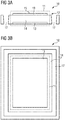
- FIG 2A a cutaway view of a further exemplary embodiment of the sensor semiconductor device 10 is shown.
- the capacitor 12 is a fringe capacitor.
- the two electrodes 13 of the capacitor 12 are arranged as combs.
- the polymer 14 is arranged between and above the electrodes 13 of the capacitor 12.
- the dashed line again marks the extent of the transducer 11.
- Figure 2B shows a top view of the exemplary embodiment of the sensor semiconductor device 10 of figure 2A .
- the two electrodes 13 are arranged as combs and the polymer 14 is arranged between and above the two electrodes 13.
- FIG 3A a cutaway view of a further exemplary embodiment of the sensor semiconductor device 10 is shown.
- the capacitor 12 is a parallel plate capacitor.
- the sensor semiconductor device 10 further comprises a trench 17 which is arranged around the transducer 11 and it provides drainage of a liquid from the top surface 15.
- the trench 17 is arranged within the polymer 14 and it preferably completely surrounds the transducer 11. This means, the trench 17 is arranged at a lower vertical position than the top surface 15 such that water droplets repelled by the top surface 15 roll off towards the trench 17.
- the trench 17 collects the liquid or the water droplets from the top surface 15 such that no other places of the transducer 11 or the sensor semiconductor device 10 are wetted by the liquid or the water droplets.
- Figure 3B shows a top view of the exemplary embodiment of the sensor semiconductor device 10 of figure 3A .
- the trench 17 surrounds the transducer 11 at all lateral sides.
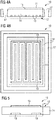
- FIG 4A a cutaway view of a further exemplary embodiment of the sensor semiconductor device 10 is shown.
- the capacitor 12 is a fringe capacitor.
- the sensor semiconductor device 10 further comprises a trench 17 which is arranged around the transducer 11 and it provides drainage of a liquid from the top surface 15.
- the top surface 15 is comprised by the polymer 14.
- Figure 4B shows a top view of the exemplary embodiment of the sensor semiconductor device 10 of figure 4A .
- the trench 17 surrounds the transducer 11 at all lateral sides.
- FIG. 5 shows a cutaway view of a further exemplary embodiment of the sensor semiconductor device 10.
- the capacitor 12 is a parallel plate capacitor.
- the capacitor 12 consists of two capacitors in series and comprises in total three electrodes 13.
- Two electrodes 13 are arranged next to each other in a plane which is parallel to the main plane of extension of the polymer 14.
- the third electrode 13 is arranged above the two other electrodes 13 in vertical direction z.
- the two electrodes 13 arranged next to each other form the bottom electrodes of the two capacitors 12 connected in series. These capacitors 12 share the third top electrode 13.
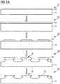
- a method for forming an exemplary embodiment of the sensor semiconductor device 10 is described.
- a first step S1 the polymer 14 is provided.
- the polymer 14 is arranged between and above the two electrodes 13 of the capacitor 12.
- the polymer 14 comprises a top layer 16 which is structured in the following steps.
- a masking layer 19 is deposited on top of the polymer 14.
- the masking layer 19 can be a photoresist layer or a hard mask layer which comprises for example silicon oxide, a nitride or a metal.
- the masking layer 19 is patterned by lithographic methods such that the masking layer 19 is removed from the polymer 14 in places. In this embodiment a regular pattern in the masking layer 19 is formed on top of the polymer 14.
- the top layer 16 of the polymer 14 is etched by wet chemical etching or by reactive ion etching through the masking layer 19. This means, the top layer 16 is only etched in the areas where the masking layer 19 is removed from the top layer 16. In this way, structures 18 are formed in the top layer 16.
- the lateral size of the structures 18 is at least 1 nm and at most 100 ⁇ m. However, the lateral size of the structures 18 is limited by the lithographic methods.
- the top layer 16 is laterally etched such that the angle between the top surface 15 and the structures 18 at the top surface 15 is less than 90°. In this way, the top surface 15 is made superhydrophobic.
- the depth of the etching and therefore the vertical height of the structures 18 can be tuned by the duration of the etching process.
- the height of the structures 18 in vertical direction z can be at least 1 nm and at most 1 ⁇ m.
- the masking layer 19 is removed. Regularly arranged structures 18 are formed within the top layer 16 of the polymer 14 such that the top surface 15 is superhydrophobic.
- the top layer 16 is laterally etched such that the masking layer 19 creates an overhang (not shown in figure 6A ).
- the fifth step S5 should be omitted.
- FIG 6B another method for forming an exemplary embodiment of the sensor semiconductor device 10 is shown.
- a first step S1 the polymer 14 is provided.
- the polymer 14 is arranged between and above the two electrodes 13 of the capacitor 12.
- a second step S2 an additional top layer 16 is deposited on top of the polymer 14. It can be advantageous to deposit an additional top layer 16 which is structured if the top layer 16 comprises a material which can be more easily structured than the polymer 14.
- a masking layer 19 is deposited on top of the top layer 16.
- a fourth step S4 the masking layer 19 is patterned by lithographic methods such that the masking layer 19 is removed from the top layer 16 in places. A regular pattern in the masking layer 19 is formed on top of the top layer 16.
- a fifth step S5 the top layer 16 is etched by wet chemical etching or by reactive ion etching through the patterned masking layer 19.
- structures 18 are formed in the top layer 16.
- the top layer 16 is laterally etched such that the angle between the top surface 15 and the structures 18 at the top surface 15 is less than 90°. In this way, the top surface 15 is made superhydrophobic. In this case the depth of the etching can also be tuned by the thickness of the top layer 16.
- a sixth step S6 the masking layer 19 is removed. Regularly arranged structures 18 are formed within the top layer 16 such that the top surface 15 is superhydrophobic.
- FIG 7A a cutaway view of a further exemplary embodiment of the sensor semiconductor device 10 with a structured top surface 15 is shown.
- the capacitor 12 is a parallel plate capacitor.
- the surface of the upper electrode 13 is structured with a regular pattern such that the top surface 15 of the transducer 11 is superhydrophobic.
- FIG 7B a cutaway view of a further exemplary embodiment of the sensor semiconductor device 10 with a structured top surface 15 is shown.
- the capacitor 12 is a fringe capacitor.
- the polymer 14 is arranged between and above the two electrodes 13 of the capacitor 12.
- the surface of the polymer 14 is structured with a regular pattern such that the top surface 15 of the transducer 11 is superhydrophobic.
- FIG 7C a cutaway view of a further exemplary embodiment of the sensor semiconductor device 10 with a structured top surface 15 is shown.
- the capacitor 12 is a parallel plate capacitor.
- the top layer 16 is structured with a regular pattern such that the top surface 15 of the transducer 11 is superhydrophobic.
- FIG 7D a cutaway view of a further exemplary embodiment of the sensor semiconductor device 10 with a structured top surface 15 is shown.
- the capacitor 12 is a fringe capacitor.
- the top layer 16 is structured with a regular pattern such that the top surface 15 of the transducer 11 is superhydrophobic.
- FIG 8A a top view on a structured top surface 15 of a sensor semiconductor device 10 is shown.
- the square-shaped structures 18 are arranged on top of the top layer 16 of the transducer 11. This means the top layer 16 can be an electrode 13, the polymer 14 or an additional top layer 16.
- the square-shaped structures 18 are formed on or within the top layer 16 and are arranged in a regular pattern.
- the contact angle ⁇ w is a measure for the hydrophobicity of a surface.
- a r x st + x sp * y st + y sp + 2 * x st * z st + 2 * y st * z st , where X st gives the size of one structure 18 in x-direction, Y st gives the size of one structure 18 in y-direction and Z st gives the size of one structure 18 in z-direction. X sp gives the distance between two neighboring structures 18 in x-direction and Y sp gives the distance between two neighboring structures 18 in y-direction.
- structures 18 that are large in x- and y-direction are giving low r-values for a constant z-value and are less effective in increasing the contact angle ⁇ w of water droplets.
- the lateral size of the structures 18 is at least 1 nm and at most 100 ⁇ m, whereas the size of the structures 18 in vertical direction z can be at least 1 nm and at most 1 ⁇ m.
- FIG 8B a cutaway view of a structured top surface 15 of the sensor semiconductor device 10 is shown.
- the square-shaped structures 18 are arranged on top of or in the top layer 16 of the transducer 11.
- a randomly structured top surface 15 of a sensor semiconductor device 10 is shown.
- the picture is obtained by scanning electron microscopy. It is shown that a top layer 16 is structured by reactive ion etching such that the top surface 15 of the transducer 11 is structured in a random pattern.
- the top surface 15 is roughened by exposure to a plasma of N 2 , O 2 and CF 4 .
Landscapes
- Chemical & Material Sciences (AREA)
- Chemical Kinetics & Catalysis (AREA)
- Electrochemistry (AREA)
- Physics & Mathematics (AREA)
- Health & Medical Sciences (AREA)
- Life Sciences & Earth Sciences (AREA)
- Analytical Chemistry (AREA)
- Biochemistry (AREA)
- General Health & Medical Sciences (AREA)
- General Physics & Mathematics (AREA)
- Immunology (AREA)
- Pathology (AREA)
- Investigating Or Analyzing Materials By The Use Of Electric Means (AREA)
Abstract
Description
- The present application relates to a sensor semiconductor device and to a method of producing a sensor semiconductor device.
- Sensor semiconductor devices can be employed to measure different parameters as for example the relative humidity or the temperature. For measuring the relative humidity a polymer which can absorb moisture out of the air can be employed. Under high humidity conditions water can condense on the top surface of the polymer or on the top of the sensor semiconductor device. In this case the polymer requires time for recovering from the high humidity conditions. This means, the water needs to diffuse out of the polymer and the condensed water droplets need to evaporate from the sensor semiconductor device. This process can require a certain time in which the sensor semiconductor device does not correctly measure the relative humidity of the environment. Furthermore, the surface of the polymer or of the sensor semiconductor device can get contaminated with dirt or dust particles which can be dissolved in or collected by water droplets. Also in this way the accuracy of the sensor semiconductor device can be negatively influenced.
- It is an objective to provide a sensor semiconductor device that overcomes the above described deficiencies.
- This objective is solved by the independent claims. Further embodiments are subject of dependent claims.
- In one embodiment of the sensor semiconductor device the sensor semiconductor device comprises a transducer which comprises a capacitor with at least two electrodes. The transducer can be capable of measuring the relative humidity in the environment of the sensor semiconductor device. The capacitor can be for example a parallel plate capacitor or a fringe capacitor. The at least two electrodes comprise an electrically conductive material.
- The transducer further comprises a polymer which is arranged between at least two electrodes of the capacitor and the transducer further comprises a top surface of the transducer. The polymer is able to absorb water and the top surface is arranged such that it is exposed to the environment of the sensor semiconductor device. The polymer can reversibly collect or absorb water from the air in the environment of the sensor semiconductor device and the dielectric constant of the polymer depends on the amount of collected water or moisture. This means, the dielectric constant of the polymer is a measure for the relative humidity in the environment of the sensor semiconductor device. As the polymer is arranged between at least two electrodes of the capacitor, the capacitance of the capacitor depends on the dielectric constant of the polymer. Therefore, also the capacitance depends on the amount of water collected by the polymer and thus on the relative humidity in the environment of the sensor semiconductor device. By measuring the capacitance of the capacitor the sensor semiconductor device can be employed as a relative humidity sensor.
- The thickness of the electrodes of the capacitor is preferably between a few nanometers and a few micrometers.
- The thickness of the polymer between the two electrodes of the capacitor is preferably at least 1 µm and at most 10 µm.
- The top surface of the transducer can also be a top surface of the sensor semiconductor device. The top surface extends in lateral directions which are parallel to the main plane of extension of the sensor semiconductor device. If the capacitor is a parallel plate capacitor the top surface can be comprised by one of the electrodes of the capacitor. It is also possible that a top layer is arranged on one of the electrodes and that the top layer comprises the top surface. The top surface is arranged at the side of the top layer or of the electrode which faces away from the polymer. If the capacitor is a fringe capacitor the top surface can be comprised by the polymer which can be arranged between and on top of the electrodes of the capacitor. It is also possible that the top layer is arranged on top of the polymer and that the top layer comprises the top surface. The top surface is arranged at the side of the top layer or of the polymer which faces away from the electrodes of the capacitor.
- At least a part of the top surface is superhydrophobic. This means at least a part of the top surface repels water. The top surface can be modified to be superhydrophobic. Therefore the top surface can be roughened or structured and the surface area is increased. The top surface can be structured by different methods. For example, the top surface can be structured by at least one of patterning, roughening, structuring by photolithography, chemical treatment, etching, ultra-violet light exposure, growth of nanostructured metal layers.
- The top surface can for example be patterned by etching. Therefore a masking layer is deposited on the top surface. The masking layer can be a photoresist layer or a hard mask layer which comprises for example silicon oxide, a nitride or a metal. The masking layer is patterned by lithographic methods such that the masking layer is removed from the top surface in places. The masking layer can be regularly patterned which is easier to produce or it is also possible that it is randomly patterned. In a next step the material below the masking layer is etched in the areas where the masking layer is removed from the top surface by wet chemical etching or by reactive ion etching. In this way, structures are formed on the top surface. The material below the masking layer can be an electrode of the capacitor, the polymer or the top layer. In a preferred embodiment the masking layer is underetched. As a final step the masking layer can be removed. It is also possible that the masking layer remains on the top surface for example if it is a hard mask.
- In another embodiment a thin sputtered metal layer is deposited as the masking layer. If the metal layer is thin enough it will form islands of metal rather than a closed layer. The islands of metal then can act as the structures as described above. However, in this way the structures are arranged in a random pattern.
- In another embodiment the top surface is roughened by reactive ion etching with for example a mixture of N2, O2 and CF4. In this case no masking layer is required.
- In another embodiment the top surface is roughened by exposure to ultraviolet light. In a next step the top surface can further be treated with 1H, 1H, 2H, 2H-Perfluorodecyltriethoxysilane. The combination of both steps makes the top surface superhydrophobic.
- In another embodiment a structured silver layer is created on the top surface by treating the top surface with KOH and AgNO3 and an additional thermal treatment and n-dodecanethiol exposure.
- The sensor semiconductor device is capable of measuring the humidity of the environment of the sensor semiconductor device. This means, for example the humidity of air in the environment of the sensor semiconductor device can be measured. For this purpose the capacitance of the capacitor is measured for example continuously or at fixed times. The capacitance relates to the relative humidity as it changes with the dielectric constant of the polymer which depends on the relative humidity. At least a part of the polymer is exposed to the air in the environment of the sensor semiconductor device such that the polymer can absorb moisture out of the air. In the case that water droplets condense on the top surface the relative humidity amounts to 100 %.
- By structuring the top surface the contact angle of water droplets on the top surface is increased in comparison to a surface which is not superhydrophobic. The contact angle of water droplets on the top surface is given by the angle between the main plane of extension of the top surface and a tangent at the surface of the water droplet at the position where the water droplet is in contact with the top surface. As the top surface is structured, water droplets are only in contact with parts of the top surface, for example with peaks of the structured surface. Consequently, water droplets on the top surface can easily roll off to other parts of the transducer. Preferably, only the top surface is superhydrophobic and no other parts of the transducer.
- If water condenses on top of the polymer the maximum capacitance value is read which corresponds to 100 % relative humidity. Advantageously, the top surface is superhydrophobic and it can be the top surface of the polymer. In this case it is hard to wet the top surface of the polymer and water droplets easily roll off from the top surface of the polymer. Therefore, the polymer does not have to recover from high humidity conditions before it can measure the relative humidity of the environment correctly again. If the water droplets stayed on the top surface of the polymer it would only measure the relative humidity correctly again after the evaporation of the water droplets. Since the top surface is at least partially superhydrophobic, water droplets are immediately repelled and a change in relative humidity can be detected by the polymer within a reasonably short recovery time.
- It is also possible that the top surface gets contaminated with particles of dust or dirt. If water droplets condense on the top surface it is advantageously possible that contaminants as dust or dirt particles are mixing with or dissolving in water droplets and are thus removed from the top surface as the water droplets roll off to other parts of the transducer.
- By avoiding a relatively long recovery time of the polymer after condensating conditions and by avoiding contaminants on the top surface of the transducer the accuracy of the measurement of the relative humidity is maintained or faster reached. In other words, the accuracy of the measurement of the relative humidity is increased under these circumstances.
- In one embodiment of the sensor semiconductor device the transducer comprises a top layer with the top surface where the top layer is structured such that at least a part of the top surface is superhydrophobic. The top layer is the topmost layer of the transducer and it comprises the top surface at the side of the top layer which faces away from the capacitor. If the capacitor is a parallel plate capacitor the top layer can be arranged on top of an electrode of the capacitor at a side of the electrode which faces away from the polymer. If the capacitor is a fringe capacitor the top layer can be arranged on top of the polymer at a side of the polymer that faces away from the capacitor. The top layer can be structured as described above for the top surface such that at least a part of the top surface is superhydrophobic.
- The top layer can be structured instead of other parts of the transducer such that at least a part of the top surface is superhydrophobic. Therefore, it is possible that the top layer comprises a material which can be easily structured in comparison to other parts of the transducer.
- In one embodiment of the sensor semiconductor device the capacitor is a plate capacitor. This means, the capacitor is a parallel plate capacitor and can comprise two electrodes which are arranged in parallel to each other. For example, the electrodes can have a rectangular shape. In this case the polymer can have the shape of a cuboid which is arranged between the two electrodes.
- In one embodiment of the sensor semiconductor device the capacitor is a fringe capacitor. This means, the capacitor can comprise two electrodes which have the shape of fingers, combs, meanders, spirals or combinations thereof. The polymer can be arranged between, above and/or below the electrodes. If the top surface comprises a regular pattern of structures the structures can be aligned with the underlying electrodes of the capacitor. However, it is also possible that the structures are not aligned with the underlying electrodes.
- In one embodiment of the sensor semiconductor device a trench is arranged around the transducer, the trench providing drainage of a liquid from the top surface. This means, the trench is arranged at a lower position than the top surface of the transducer such that water droplets repelled by the top surface roll off towards the trench. The trench can be arranged around the transducer from all sides or it can only partially surround the transducer. Advantageously, the trench collects the liquid or the water droplets from the top surface such that no other places of the transducer or the sensor semiconductor device are wetted by the liquid or the water droplets.
- In one embodiment of the sensor semiconductor device, structures are formed within the top surface by photolithography, where the size of the structures is at least 1 nm and at most 100 µm in lateral directions which are parallel to the main plane of extension of the transducer, and at least 1 nm and at most 1 µm in vertical direction, which is perpendicular to the main plane of extension of the transducer. By forming the structures within the top surface, at least a part of the top surface is made superhydrophobic.
- Furthermore, a method of producing a sensor semiconductor device is provided. Preferably, the sensor semiconductor device can be produced by means of a method described herein. In other words, all features disclosed for the sensor semiconductor device are also disclosed for the method and vice versa.
- According to at least one embodiment of the method of producing a sensor semiconductor device, the method comprises forming a transducer which comprises a capacitor with at least two electrodes. The transducer can be capable of measuring the relative humidity in the environment of the sensor semiconductor device. The capacitor can be for example a parallel plate capacitor or a fringe capacitor. The at least two electrodes comprise an electrically conductive material.
- The method further comprises arranging a polymer between at least two electrodes of the capacitor. The polymer is able to absorb water. The polymer can reversibly collect or absorb water from the air in the environment of the sensor semiconductor device and the dielectric constant of the polymer depends on the amount of collected water or moisture. This means, the dielectric constant of the polymer is a measure for the relative humidity in the environment of the sensor semiconductor device. As the polymer is arranged between at least two electrodes of the capacitor the capacitance of the capacitor depends on the dielectric constant of the polymer. Therefore, also the capacitance depends on the amount of water collected by the polymer and thus on the relative humidity in the environment of the sensor semiconductor device. By measuring the capacitance of the capacitor the sensor semiconductor device can be employed as a relative humidity sensor.
- The method further comprises structuring a top layer of the transducer such that a top surface of the top layer is at least partially superhydrophobic. The top surface is arranged such that it is exposed to the environment of the sensor semiconductor device. This means at least a part of the top surface repels water. The top surface can be modified to be superhydrophobic. Therefore the top surface can be roughened or structured and the surface area is increased. The top surface can be structured by different methods.
- Moreover, the sensor semiconductor device is capable of measuring the humidity of the environment of the sensor semiconductor device. This means, for example the humidity of air in the environment of the sensor semiconductor device can be measured. For this purpose the capacitance of the capacitor is measured for example continuously or at fixed times. The capacitance relates to the relative humidity as it changes with the dielectric constant of the polymer which depends on the relative humidity. At least a part of the polymer is exposed to the air in the environment of the sensor semiconductor device such that the polymer can absorb moisture out of the air. In the case that water droplets condense on the top surface the humidity amounts to 100 %.
- As described above for the sensor semiconductor device the accuracy of the measurement of the relative humidity is maintained or faster recovered since the top surface is at least partially superhydrophobic. In other words, the accuracy of the measurement of the relative humidity is increased under these circumstances. In this way, a recovery time of the polymer after high humidity conditions and contaminants on the top surface of the transducer can be avoided.
- According to at least one embodiment of the method the top layer is comprised by the polymer. This means, the polymer is the topmost part or layer of the transducer. The top layer is arranged at the side of the polymer which faces away from the capacitor. The polymer can be the topmost part or layer of the transducer for example if the capacitor is a fringe capacitor and the polymer is arranged between and above the electrodes of the capacitor. In this case the polymer is structured or roughened such that the top surface is at least partially superhydrophobic.
- According to at least one embodiment of the method the top layer is comprised by an electrode of the capacitor. This means, the electrode is the topmost part of the transducer. If the capacitor is a plate capacitor the polymer can be arranged between the two electrodes of the capacitor such that one of the electrodes is the topmost part of the transducer. In this case the electrode is structured or roughened such that the top surface is at least partially superhydrophobic.
- According to at least one embodiment of the method the top layer is comprised neither by the polymer nor by an electrode of the capacitor. The top layer can be a separate layer which is not comprised by the capacitor. The top layer can be arranged on top of the capacitor in vertical direction. It is also possible that the top layer is arranged on top of the polymer in vertical direction.
- According to at least one embodiment of the method the capacitor is a plate capacitor. This means, the capacitor can comprise two electrodes which are arranged in parallel to each other. For example, the electrodes can have a rectangular shape. In this case the polymer can have the shape of a cuboid which is arranged between the two electrodes.
- According to at least one embodiment of the method the capacitor is a fringe capacitor. This means, the capacitor can comprise two electrodes which have the shape of fingers, combs, meanders, spirals or combinations thereof. The polymer can be arranged between, above and/or below the electrodes. If the top surface comprises a regular pattern of structures, the structures can be aligned with the underlying electrodes of the capacitor. However, it is also possible that the structures are not aligned with the underlying electrodes.
- According to at least one embodiment of the method a trench is arranged around the transducer, the trench providing drainage of a liquid from the top surface. This means, the trench is arranged at a lower position than the top surface of the transducer such that water droplets repelled by the top surface roll off towards the trench. The trench can be arranged around the transducer from all sides or it can only partially surround the transducer. Advantageously, the trench collects the liquid or the water droplets from the top surface such that no other places of the transducer or the sensor semiconductor device are wetted by the liquid or the water droplets.
- According to at least one embodiment of the method the structuring of the top layer involves at least one of the following:
- patterning,
- roughening,
- structuring by photolithography,
- chemical treatment,
- etching,
- ultra-violet light exposure,
- growth of nanostructured metal layers.
- The top layer can for example be patterned by etching. Therefore a masking layer is deposited on top of the top layer. The masking layer can be a photoresist layer or a hard mask layer which comprises for example silicon oxide, a nitride or a metal. The masking layer is patterned by lithographic methods such that the masking layer is removed from the top layer in places. The masking layer can be regularly patterned which is easier to produce or it is also possible that it is randomly patterned. In a next step the top layer is etched in the areas where the masking layer is removed from the top surface by wet chemical etching or by reactive ion etching. In this way, structures are formed on or within the top layer. In a preferred embodiment the masking layer is underetched. As a final step the masking layer can be removed. It is also possible that the masking layer remains on top of the top layer for example if it is a hard mask.
- In another embodiment a thin sputtered metal layer is deposited as the masking layer. If the metal layer is thin enough it will form islands of metal rather than a closed layer. The islands of metal then can act as a masking layer as described above. However, in this way the structures are arranged in a random pattern.
- In another embodiment the top layer is roughened by reactive ion etching with for example a mixture of N2, O2 and CF4. In this case no masking layer is required.
- In another embodiment the top layer is roughened by exposure to ultraviolet light. In a next step the top layer can further be treated with with 1H, 1H, 2H, 2H-Perfluorodecyltriethoxysilane. The combination of these steps makes the top surface superhydrophobic.
- In another embodiment a structured silver layer is created on top of the top layer by treating the top surface with KOH and AgNO3 and an additional thermal treatment and n-dodecanethiol exposure.
- According to at least one embodiment of the method structures are formed within the top layer by photolithography, where the size of the structures is at least 1 nm and at most 100 µm in lateral directions which are parallel to the main plane of extension of the transducer. The size of the structures in vertical direction which is perpendicular to the lateral directions can be at least 1 nm and at most 1 µm. By forming the structures within the top layer, at least a part of the top surface is made superhydrophobic.
- The following description of figures may further illustrate and explain exemplary embodiments. Components that are functionally identical or have an identical effect are denoted by identical references. Identical or effectively identical components might be described only with respect to the figures where they occur first. Their description is not necessarily repeated in successive figures.
-
Figure 1A shows a cutaway view of an exemplary embodiment of a sensor semiconductor device. -
Figure 1B shows a top view of the exemplary embodiment of the sensor semiconductor device offigure 1A . - With
figures 2A, 2B ,3A, 3B ,4A and 4B further exemplary embodiments of the sensor semiconductor device are shown. -
Figure 5 shows a cutaway view of another exemplary embodiment of the sensor semiconductor device. - With
figure 6A a method for forming an exemplary embodiment of the sensor semiconductor device is described. - In
figure 6B another method for forming an exemplary embodiment of the sensor semiconductor device is shown. - In
figures 7A, 7B, 7C and 7D further exemplary embodiments of the sensor semiconductor device with a structured top surface are shown. - In
figures 8A and 8B a top view and a cutaway view on a structured top surface of the sensor semiconductor device are shown. - In
figure 9 a randomly structured top surface of a sensor semiconductor device is shown. - In
figure 1A a cutaway view of an exemplary embodiment of asensor semiconductor device 10 is shown. Thesensor semiconductor device 10 comprises atransducer 11 which comprises acapacitor 12. In this embodiment thecapacitor 12 is a parallel plate capacitor. Thecapacitor 12 comprises twoelectrodes 13 which are arranged at a distance from each other. The twoelectrodes 13 are arranged parallel to each other and they are arranged on top of each other in vertical direction z which is perpendicular to the main plane of extension of thetransducer 11. Apolymer 14 is arranged between the twoelectrodes 13. Thepolymer 14 has a larger extent in a lateral direction x than the twoelectrodes 13. The lateral direction x is perpendicular to the vertical direction z. The dashed line marks the extent of thetransducer 11. - The
polymer 14 is able to absorb water. Thepolymer 14 can reversibly collect or absorb water from the air in the environment of thesensor semiconductor device 10 and the dielectric constant of thepolymer 14 depends on the amount of collected water or moisture. - The
transducer 11 further comprises atop surface 15. In this embodiment thetop surface 15 is comprised by theupper electrode 13. Thetop surface 15 is arranged such that it is exposed to the environment of thesensor semiconductor device 10 and at least a part of thetop surface 15 is superhydrophobic. -
Figure 1B shows a top view of the exemplary embodiment of thesensor semiconductor device 10 offigure 1A . Theupper electrode 13 is shown from the top and thepolymer 14 has a larger lateral extent than theelectrodes 13 of thecapacitor 12. - In
figure 2A a cutaway view of a further exemplary embodiment of thesensor semiconductor device 10 is shown. In this embodiment thecapacitor 12 is a fringe capacitor. This means, the twoelectrodes 13 of thecapacitor 12 are arranged as combs. Thepolymer 14 is arranged between and above theelectrodes 13 of thecapacitor 12. The dashed line again marks the extent of thetransducer 11. -
Figure 2B shows a top view of the exemplary embodiment of thesensor semiconductor device 10 offigure 2A . The twoelectrodes 13 are arranged as combs and thepolymer 14 is arranged between and above the twoelectrodes 13. - In
figure 3A a cutaway view of a further exemplary embodiment of thesensor semiconductor device 10 is shown. Thecapacitor 12 is a parallel plate capacitor. In addition to the embodiment shown infigure 1A thesensor semiconductor device 10 further comprises atrench 17 which is arranged around thetransducer 11 and it provides drainage of a liquid from thetop surface 15. Thetrench 17 is arranged within thepolymer 14 and it preferably completely surrounds thetransducer 11. This means, thetrench 17 is arranged at a lower vertical position than thetop surface 15 such that water droplets repelled by thetop surface 15 roll off towards thetrench 17. Advantageously, thetrench 17 collects the liquid or the water droplets from thetop surface 15 such that no other places of thetransducer 11 or thesensor semiconductor device 10 are wetted by the liquid or the water droplets. -
Figure 3B shows a top view of the exemplary embodiment of thesensor semiconductor device 10 offigure 3A . Thetrench 17 surrounds thetransducer 11 at all lateral sides. - In
figure 4A a cutaway view of a further exemplary embodiment of thesensor semiconductor device 10 is shown. Thecapacitor 12 is a fringe capacitor. In addition to the embodiment shown infigure 2A thesensor semiconductor device 10 further comprises atrench 17 which is arranged around thetransducer 11 and it provides drainage of a liquid from thetop surface 15. Thetop surface 15 is comprised by thepolymer 14. -
Figure 4B shows a top view of the exemplary embodiment of thesensor semiconductor device 10 offigure 4A . Thetrench 17 surrounds thetransducer 11 at all lateral sides. -
Figure 5 shows a cutaway view of a further exemplary embodiment of thesensor semiconductor device 10. Thecapacitor 12 is a parallel plate capacitor. In difference to the embodiment shown infigure 1A thecapacitor 12 consists of two capacitors in series and comprises in total threeelectrodes 13. Twoelectrodes 13 are arranged next to each other in a plane which is parallel to the main plane of extension of thepolymer 14. Thethird electrode 13 is arranged above the twoother electrodes 13 in vertical direction z. The twoelectrodes 13 arranged next to each other form the bottom electrodes of the twocapacitors 12 connected in series. Thesecapacitors 12 share the thirdtop electrode 13. - With
figure 6A a method for forming an exemplary embodiment of thesensor semiconductor device 10 is described. In a first step S1 thepolymer 14 is provided. Thepolymer 14 is arranged between and above the twoelectrodes 13 of thecapacitor 12. Thepolymer 14 comprises atop layer 16 which is structured in the following steps. - In a second step S2 a
masking layer 19 is deposited on top of thepolymer 14. Themasking layer 19 can be a photoresist layer or a hard mask layer which comprises for example silicon oxide, a nitride or a metal. - In the third step S3 the
masking layer 19 is patterned by lithographic methods such that themasking layer 19 is removed from thepolymer 14 in places. In this embodiment a regular pattern in themasking layer 19 is formed on top of thepolymer 14. - In the fourth step S4 the
top layer 16 of thepolymer 14 is etched by wet chemical etching or by reactive ion etching through themasking layer 19. This means, thetop layer 16 is only etched in the areas where themasking layer 19 is removed from thetop layer 16. In this way,structures 18 are formed in thetop layer 16. The lateral size of thestructures 18 is at least 1 nm and at most 100 µm. However, the lateral size of thestructures 18 is limited by the lithographic methods. Thetop layer 16 is laterally etched such that the angle between thetop surface 15 and thestructures 18 at thetop surface 15 is less than 90°. In this way, thetop surface 15 is made superhydrophobic. The depth of the etching and therefore the vertical height of thestructures 18 can be tuned by the duration of the etching process. The height of thestructures 18 in vertical direction z can be at least 1 nm and at most 1 µm. - In the fifth step S5 the
masking layer 19 is removed. Regularly arrangedstructures 18 are formed within thetop layer 16 of thepolymer 14 such that thetop surface 15 is superhydrophobic. - Alternatively, in the fourth step S4 the
top layer 16 is laterally etched such that themasking layer 19 creates an overhang (not shown infigure 6A ). In this case the fifth step S5 should be omitted. - In
figure 6B another method for forming an exemplary embodiment of thesensor semiconductor device 10 is shown. In a first step S1 thepolymer 14 is provided. Thepolymer 14 is arranged between and above the twoelectrodes 13 of thecapacitor 12. - In a second step S2 an additional
top layer 16 is deposited on top of thepolymer 14. It can be advantageous to deposit an additionaltop layer 16 which is structured if thetop layer 16 comprises a material which can be more easily structured than thepolymer 14. - In a third step S3 a
masking layer 19 is deposited on top of thetop layer 16. - In a fourth step S4 the
masking layer 19 is patterned by lithographic methods such that themasking layer 19 is removed from thetop layer 16 in places. A regular pattern in themasking layer 19 is formed on top of thetop layer 16. - In a fifth step S5 the
top layer 16 is etched by wet chemical etching or by reactive ion etching through the patternedmasking layer 19. Thus,structures 18 are formed in thetop layer 16. Thetop layer 16 is laterally etched such that the angle between thetop surface 15 and thestructures 18 at thetop surface 15 is less than 90°. In this way, thetop surface 15 is made superhydrophobic. In this case the depth of the etching can also be tuned by the thickness of thetop layer 16. - In a sixth step S6 the
masking layer 19 is removed. Regularly arrangedstructures 18 are formed within thetop layer 16 such that thetop surface 15 is superhydrophobic. - In
figure 7A a cutaway view of a further exemplary embodiment of thesensor semiconductor device 10 with a structuredtop surface 15 is shown. Thecapacitor 12 is a parallel plate capacitor. The surface of theupper electrode 13 is structured with a regular pattern such that thetop surface 15 of thetransducer 11 is superhydrophobic. - In
figure 7B a cutaway view of a further exemplary embodiment of thesensor semiconductor device 10 with a structuredtop surface 15 is shown. Thecapacitor 12 is a fringe capacitor. Thepolymer 14 is arranged between and above the twoelectrodes 13 of thecapacitor 12. The surface of thepolymer 14 is structured with a regular pattern such that thetop surface 15 of thetransducer 11 is superhydrophobic. - In
figure 7C a cutaway view of a further exemplary embodiment of thesensor semiconductor device 10 with a structuredtop surface 15 is shown. Thecapacitor 12 is a parallel plate capacitor. On top of theupper electrode 13 an additionaltop layer 16 is arranged. Thetop layer 16 is structured with a regular pattern such that thetop surface 15 of thetransducer 11 is superhydrophobic. - In
figure 7D a cutaway view of a further exemplary embodiment of thesensor semiconductor device 10 with a structuredtop surface 15 is shown. Thecapacitor 12 is a fringe capacitor. On top of thepolymer 14 an additionaltop layer 16 is arranged. Thetop layer 16 is structured with a regular pattern such that thetop surface 15 of thetransducer 11 is superhydrophobic. - In
figure 8A a top view on a structuredtop surface 15 of asensor semiconductor device 10 is shown. The square-shapedstructures 18 are arranged on top of thetop layer 16 of thetransducer 11. This means thetop layer 16 can be anelectrode 13, thepolymer 14 or an additionaltop layer 16. The square-shapedstructures 18 are formed on or within thetop layer 16 and are arranged in a regular pattern. - If water droplets condense on the structured
top surface 15 the contact angle θw of the water droplets is given by:
- The real surface area Ar is given by:

structure 18 in x-direction, Yst gives the size of onestructure 18 in y-direction and Zst gives the size of onestructure 18 in z-direction. Xsp gives the distance between two neighboringstructures 18 in x-direction and Ysp gives the distance between two neighboringstructures 18 in y-direction. - The projected surface area Ap is given by:

- Therefore,
structures 18 that are large in x- and y-direction are giving low r-values for a constant z-value and are less effective in increasing the contact angle θw of water droplets. Thus, the lateral size of thestructures 18 is at least 1 nm and at most 100 µm, whereas the size of thestructures 18 in vertical direction z can be at least 1 nm and at most 1 µm. - In
figure 8B a cutaway view of a structuredtop surface 15 of thesensor semiconductor device 10 is shown. The square-shapedstructures 18 are arranged on top of or in thetop layer 16 of thetransducer 11. - In
figure 9 a randomly structuredtop surface 15 of asensor semiconductor device 10 is shown. The picture is obtained by scanning electron microscopy. It is shown that atop layer 16 is structured by reactive ion etching such that thetop surface 15 of thetransducer 11 is structured in a random pattern. Thetop surface 15 is roughened by exposure to a plasma of N2, O2 and CF4. -
- 10:
- sensor semiconductor device
- 11:
- transducer
- 12:
- capacitor
- 13:
- electrode
- 14:
- polymer
- 15:
- top surface
- 16:
- top layer
- 17:
- trench
- 18:
- structure
- 19:
- masking layer
- S1:
- first step
- S2:
- second step
- S3:
- third step
- S4:
- fourth step
- S5:
- fifth step
- S6:
- sixth step
- Ar :
- real surface area
- Ap :
- projected surface area
- r:
- ratio
- θw :
- contact angle
- Xst :
- size
- Yst :
- size
- Zst :
- size
- Xsp :
- distance
- Ysp :
- distance
- x:
- lateral direction
- y:
- lateral direction
- z:
- vertical direction
Claims (15)
- A sensor semiconductor device (10), comprising:- a transducer (11) which comprises:- a capacitor (12) with at least two electrodes (13),- a polymer (14) which is arranged between at least two electrodes (13) of the capacitor (12), and- a top surface (15) of the transducer (11), wherein- the polymer (14) is able to absorb water,- the top surface (15) is arranged such that it is exposed to the environment of the sensor semiconductor device (10),- at least a part of the top surface (15) is superhydrophobic, and- the sensor semiconductor device (10) is capable of measuring the humidity of the environment of the sensor semiconductor device (10).
- The sensor semiconductor device (10) according to claim 1, wherein the transducer (11) comprises a top layer (16) with the top surface (15) where the top layer (16) is structured such that at least a part of the top surface (15) is superhydrophobic.
- The sensor semiconductor device (10) according to one of the preceding claims, wherein the capacitor (12) is a plate capacitor.
- The sensor semiconductor device (10) according to one of claims 1 or 2, wherein the capacitor (12) is a fringe capacitor.
- The sensor semiconductor device (10) according to one of the preceding claims, wherein a trench (17) is arranged around the transducer (11), the trench (17) providing drainage of a liquid from the top surface (15).
- The sensor semiconductor device (10) according to one of the preceding claims, wherein structures (18) are formed within the top surface (15) by photolithography, where the size of the structures (18) is at least 1 nm and at most 100 µm in lateral directions (x, y) which are parallel to the main plane of extension of the transducer (11), and at least 1 nm and at most 1 µm in vertical direction (z), which is perpendicular to the main plane of extension of the transducer (11).
- Method of producing a sensor semiconductor device (10), comprising:- forming a transducer (11) which comprises a capacitor (12) with at least two electrodes (13),- arranging a polymer (14) between at least two electrodes (13) of the capacitor (12), and- structuring a top layer (16) of the transducer (11) such that a top surface (15) of the top layer (16) is at least partially superhydrophobic, wherein- the polymer (14) is able to absorb water,- the top surface (15) is arranged such that it is exposed to the environment of the sensor semiconductor device (10), and- the sensor semiconductor device (10) is capable of measuring the humidity of the environment of the sensor semiconductor device (10).
- The method of producing a sensor semiconductor device (10) according to claim 7, wherein the top layer (16) is comprised by the polymer (14).
- The method of producing a sensor semiconductor device (10) according to claim 7, wherein the top layer (16) is comprised by an electrode (13) of the capacitor (12).
- The method of producing a sensor semiconductor device (10) according to claim 7, wherein the top layer (16) is comprised neither by the polymer (14) nor by an electrode (13) of the capacitor (12).
- The method of producing a sensor semiconductor device (10) according to one of claims 7 to 10, wherein the capacitor (12) is a plate capacitor.
- The method of producing a sensor semiconductor device (10) according to one of claims 7 to 10, wherein the capacitor (12) is a fringe capacitor.
- The method of producing a sensor semiconductor device (10) according to one of claims 7 to 12, wherein a trench (17) is arranged around the transducer (11), the trench (17) providing drainage of a liquid from the top surface (15).
- The method of producing a sensor semiconductor device (10) according to one of claims 7 to 13, wherein the structuring of the top layer (16) involves at least one of the following:- patterning,- roughening,- structuring by photolithography,- chemical treatment,- etching,- ultra-violet light exposure,- growth of nanostructured metal layers.
- The method of producing a sensor semiconductor device (10) according to claim 14, wherein structures (18) are formed within the top layer (16) by photolithography, where the size of the structures (18) is at least 1 nm and at most 100 µm in lateral directions (x, y) which are parallel to the main plane of extension of the transducer (11).
Priority Applications (5)
| Application Number | Priority Date | Filing Date | Title |
|---|---|---|---|
| EP17170184.0A EP3401674B1 (en) | 2017-05-09 | 2017-05-09 | Capacitive-type humidity sensor with superhydrophobic top surface and corresponding fabrication method |
| TW107113693A TWI672770B (en) | 2017-05-09 | 2018-04-23 | Sensor semiconductor device and method of produsing the same |
| US16/611,805 US11262325B2 (en) | 2017-05-09 | 2018-05-04 | Sensor semiconductor device |
| CN201880030655.XA CN110651180B (en) | 2017-05-09 | 2018-05-04 | Super-hydrophobic capacitive humidity sensor and manufacturing method thereof |
| PCT/EP2018/061525 WO2018206432A1 (en) | 2017-05-09 | 2018-05-04 | Superhydrophobic capacitive-type humidity sensor and corresponding fabrication method |
Applications Claiming Priority (1)
| Application Number | Priority Date | Filing Date | Title |
|---|---|---|---|
| EP17170184.0A EP3401674B1 (en) | 2017-05-09 | 2017-05-09 | Capacitive-type humidity sensor with superhydrophobic top surface and corresponding fabrication method |
Publications (2)
| Publication Number | Publication Date |
|---|---|
| EP3401674A1 true EP3401674A1 (en) | 2018-11-14 |
| EP3401674B1 EP3401674B1 (en) | 2020-07-15 |
Family
ID=58709239
Family Applications (1)
| Application Number | Title | Priority Date | Filing Date |
|---|---|---|---|
| EP17170184.0A Active EP3401674B1 (en) | 2017-05-09 | 2017-05-09 | Capacitive-type humidity sensor with superhydrophobic top surface and corresponding fabrication method |
Country Status (5)
| Country | Link |
|---|---|
| US (1) | US11262325B2 (en) |
| EP (1) | EP3401674B1 (en) |
| CN (1) | CN110651180B (en) |
| TW (1) | TWI672770B (en) |
| WO (1) | WO2018206432A1 (en) |
Cited By (1)
| Publication number | Priority date | Publication date | Assignee | Title |
|---|---|---|---|---|
| US11262325B2 (en) | 2017-05-09 | 2022-03-01 | Sciosense B.V. | Sensor semiconductor device |
Families Citing this family (3)
| Publication number | Priority date | Publication date | Assignee | Title |
|---|---|---|---|---|
| TWI741826B (en) * | 2020-10-12 | 2021-10-01 | 國立清華大學 | Sensing device, humidity sensing chip and method of manufacturing the device |
| CN121039470A (en) | 2023-05-09 | 2025-11-28 | 希奥检测有限公司 | Sensor module and method for manufacturing sensor module |
| DE102023119941A1 (en) | 2023-05-09 | 2024-11-14 | Sciosense B.V. | Sensor module and method for producing a sensor module |
Citations (5)
| Publication number | Priority date | Publication date | Assignee | Title |
|---|---|---|---|---|
| JP2003262600A (en) * | 2002-03-07 | 2003-09-19 | Tdk Corp | Humidity sensor element and method of manufacturing the same |
| JP2012068054A (en) * | 2010-09-21 | 2012-04-05 | Denso Corp | Capacitance type sensor and control device |
| US20130139587A1 (en) * | 2011-12-02 | 2013-06-06 | Stmicroelectronics Pte Ltd. | Tunable humidity sensor with integrated heater |
| JP2015161600A (en) * | 2014-02-27 | 2015-09-07 | 株式会社デンソー | Humidity sensor |
| CN104914139A (en) * | 2015-06-15 | 2015-09-16 | 兰州交通大学 | A Fast Response Capacitive Humidity Sensing Element with Hole-shaped Upper Electrode and Humidity-Sensing Film Parallel Plate |
Family Cites Families (24)
| Publication number | Priority date | Publication date | Assignee | Title |
|---|---|---|---|---|
| EP1369683A4 (en) | 2001-03-13 | 2008-06-18 | Tdk Corp | Humidity sensor element and method for manufacture thereof |
| DE10335163B3 (en) | 2003-07-30 | 2005-03-03 | Micronas Gmbh | gas sensor |
| JP5112639B2 (en) * | 2006-03-06 | 2013-01-09 | トウプラスエンジニアリング株式会社 | Humidity sensor |
| TW200819739A (en) * | 2006-10-27 | 2008-05-01 | Mercury Microsystems Company Ltd | Miniatured humidity sensor having a non-coplanar electrode and moisture entry/exit |
| TWI381536B (en) * | 2008-08-29 | 2013-01-01 | 國立臺灣大學 | Micro-nano structure PN diode array thin film solar cell and manufacturing method thereof |
| JP5146596B2 (en) * | 2009-04-30 | 2013-02-20 | 株式会社村田製作所 | Biosensor device |
| US20110166045A1 (en) * | 2009-12-01 | 2011-07-07 | Anuj Dhawan | Wafer scale plasmonics-active metallic nanostructures and methods of fabricating same |
| GB2476093A (en) * | 2009-12-11 | 2011-06-15 | Manvers Engineering Ltd | Oil Collecting Device Made Of Hydrophobic And Oleophilic Materials. |
| US9956743B2 (en) * | 2010-12-20 | 2018-05-01 | The Regents Of The University Of California | Superhydrophobic and superoleophobic nanosurfaces |
| FR2991456B1 (en) * | 2012-06-04 | 2023-02-10 | Commissariat Energie Atomique | CAPACITIVE HUMIDITY SENSOR WITH GRAPHENE ELECTRODE |
| US9080928B2 (en) * | 2013-01-11 | 2015-07-14 | Nokia Technologies Oy | Apparatus and associated methods |
| KR101569460B1 (en) | 2013-02-08 | 2015-11-16 | 국민대학교 산학협력단 | superamphiphobic structure and method of manufacturing the same |
| US10175188B2 (en) | 2013-03-15 | 2019-01-08 | Robert Bosch Gmbh | Trench based capacitive humidity sensor |
| US9044943B2 (en) * | 2013-04-03 | 2015-06-02 | Palo Alto Research Center Incorporated | Inkjet printhead incorporating oleophobic membrane |
| US9171810B2 (en) | 2013-11-21 | 2015-10-27 | Nxp B.V. | Electronic device incorporating a randomized interconnection layer having a randomized conduction pattern |
| EP3172582B1 (en) * | 2014-07-22 | 2025-05-21 | Brewer Science Inc. | Thin-film resistive-based sensor |
| WO2016056887A1 (en) * | 2014-10-09 | 2016-04-14 | Mimos Berhad | Humidity sensor with nanoporous polyimide membranes and a method of fabrication thereof |
| EP3043173B1 (en) | 2015-01-09 | 2017-09-06 | Honeywell International Inc. | A humidity sensor |
| EP3259581B1 (en) | 2015-02-17 | 2020-01-29 | Honeywell International Inc. | Humidity sensor and method for manufacturing the sensor |
| JP6535185B2 (en) | 2015-03-04 | 2019-06-26 | エイブリック株式会社 | Humidity sensor |
| TWI591329B (en) * | 2015-09-04 | 2017-07-11 | 鑫廣生醫科技股份有限公司 | Test strip with capacity of sensing humidity |
| EP3168866B1 (en) | 2015-11-16 | 2020-12-30 | ams AG | Semiconductor humidity sensor device and manufacturing method thereof |
| US10948448B2 (en) | 2016-09-30 | 2021-03-16 | Minebea Mitsumi Inc. | Humidity sensor |
| EP3401674B1 (en) | 2017-05-09 | 2020-07-15 | ams International AG | Capacitive-type humidity sensor with superhydrophobic top surface and corresponding fabrication method |
-
2017
- 2017-05-09 EP EP17170184.0A patent/EP3401674B1/en active Active
-
2018
- 2018-04-23 TW TW107113693A patent/TWI672770B/en active
- 2018-05-04 CN CN201880030655.XA patent/CN110651180B/en active Active
- 2018-05-04 US US16/611,805 patent/US11262325B2/en active Active
- 2018-05-04 WO PCT/EP2018/061525 patent/WO2018206432A1/en not_active Ceased
Patent Citations (5)
| Publication number | Priority date | Publication date | Assignee | Title |
|---|---|---|---|---|
| JP2003262600A (en) * | 2002-03-07 | 2003-09-19 | Tdk Corp | Humidity sensor element and method of manufacturing the same |
| JP2012068054A (en) * | 2010-09-21 | 2012-04-05 | Denso Corp | Capacitance type sensor and control device |
| US20130139587A1 (en) * | 2011-12-02 | 2013-06-06 | Stmicroelectronics Pte Ltd. | Tunable humidity sensor with integrated heater |
| JP2015161600A (en) * | 2014-02-27 | 2015-09-07 | 株式会社デンソー | Humidity sensor |
| CN104914139A (en) * | 2015-06-15 | 2015-09-16 | 兰州交通大学 | A Fast Response Capacitive Humidity Sensing Element with Hole-shaped Upper Electrode and Humidity-Sensing Film Parallel Plate |
Non-Patent Citations (1)
| Title |
|---|
| XI ZHANG ET AL: "Superhydrophobic surfaces: from structural control to functional application", JOURNAL OF MATERIALS CHEMISTRY, vol. 18, no. 6, 14 November 2007 (2007-11-14), GB, pages 621 - 633, XP055400860, ISSN: 0959-9428, DOI: 10.1039/B711226B * |
Cited By (1)
| Publication number | Priority date | Publication date | Assignee | Title |
|---|---|---|---|---|
| US11262325B2 (en) | 2017-05-09 | 2022-03-01 | Sciosense B.V. | Sensor semiconductor device |
Also Published As
| Publication number | Publication date |
|---|---|
| TW201901872A (en) | 2019-01-01 |
| WO2018206432A1 (en) | 2018-11-15 |
| EP3401674B1 (en) | 2020-07-15 |
| TWI672770B (en) | 2019-09-21 |
| US11262325B2 (en) | 2022-03-01 |
| US20200064295A1 (en) | 2020-02-27 |
| CN110651180A (en) | 2020-01-03 |
| CN110651180B (en) | 2022-09-06 |
Similar Documents
| Publication | Publication Date | Title |
|---|---|---|
| US11262325B2 (en) | Sensor semiconductor device | |
| KR950015770A (en) | Capacitor Manufacturing Method of Semiconductor Device | |
| US8371168B2 (en) | In-plane sensor and method for making same | |
| US7795062B2 (en) | Method of forming a pressure switch thin film device | |
| EP0371069A1 (en) | Process for manufacturing microsensors with integrated signal processing | |
| DE102011112879A1 (en) | Semiconductor manufacturing and semiconductor device with semiconductor structure | |
| KR20130063072A (en) | Method of forming a pattern structure and method of forming a capacitor | |
| US20100024549A1 (en) | In-Plane Sensor, Out-of-Plane Sensor, and Method for Making Same | |
| US8640543B2 (en) | Micro-electro-mechanical system device, out-of-plane sensor and method for making micro-electro-mechanical system device | |
| KR100489157B1 (en) | Method for manufacturing semiconductor device and semiconductor device | |
| JPH0582747A (en) | Semiconductor device | |
| JP4193232B2 (en) | Mechanical quantity sensor | |
| CN1657927A (en) | CMOS Process Compatible Relative Humidity Sensor | |
| US8117919B2 (en) | Micro-electro-mechanical system device | |
| US9096426B2 (en) | Electronic device structure and method of making electronic devices and integrated circuits using grayscale technology and multilayer thin-film composites | |
| JP3508286B2 (en) | Manufacturing method of semiconductor dynamic quantity sensor | |
| KR970010569B1 (en) | Fabrication method of semiconductor device | |
| CN101726629B (en) | Micro-electromechanical element, out-of-plane sensor and manufacturing method of micro-electromechanical element | |
| CN114171376B (en) | A method for patterning semiconductors | |
| CN109299630B (en) | Semiconductor fingerprint sensor and manufacturing method thereof | |
| TWI784580B (en) | Piezoelectric mems accelerometer and method for manufacturing the same | |
| DE102024209168A1 (en) | Microelectromechanical sensor component, microelectromechanical inertial sensor and method for manufacturing a microelectromechanical sensor component | |
| CN118795172A (en) | An acceleration sensor based on a highly conductive two-dimensional thin film suspended SiO₂/Si mass block on an SOI substrate and a preparation method thereof | |
| DE102006049886B4 (en) | Micromechanical component with a vibratable micromechanical structure, sensor component and method for producing a component | |
| CN118016651A (en) | Capacitor structure and method of forming the same |
Legal Events
| Date | Code | Title | Description |
|---|---|---|---|
| PUAI | Public reference made under article 153(3) epc to a published international application that has entered the european phase |
Free format text: ORIGINAL CODE: 0009012 |
|
| STAA | Information on the status of an ep patent application or granted ep patent |
Free format text: STATUS: THE APPLICATION HAS BEEN PUBLISHED |
|
| AK | Designated contracting states |
Kind code of ref document: A1 Designated state(s): AL AT BE BG CH CY CZ DE DK EE ES FI FR GB GR HR HU IE IS IT LI LT LU LV MC MK MT NL NO PL PT RO RS SE SI SK SM TR |
|
| AX | Request for extension of the european patent |
Extension state: BA ME |
|
| STAA | Information on the status of an ep patent application or granted ep patent |
Free format text: STATUS: REQUEST FOR EXAMINATION WAS MADE |
|
| 17P | Request for examination filed |
Effective date: 20190327 |
|
| RBV | Designated contracting states (corrected) |
Designated state(s): AL AT BE BG CH CY CZ DE DK EE ES FI FR GB GR HR HU IE IS IT LI LT LU LV MC MK MT NL NO PL PT RO RS SE SI SK SM TR |
|
| STAA | Information on the status of an ep patent application or granted ep patent |
Free format text: STATUS: EXAMINATION IS IN PROGRESS |
|
| 17Q | First examination report despatched |
Effective date: 20190625 |
|
| GRAP | Despatch of communication of intention to grant a patent |
Free format text: ORIGINAL CODE: EPIDOSNIGR1 |
|
| STAA | Information on the status of an ep patent application or granted ep patent |
Free format text: STATUS: GRANT OF PATENT IS INTENDED |
|
| INTG | Intention to grant announced |
Effective date: 20200219 |
|
| GRAS | Grant fee paid |
Free format text: ORIGINAL CODE: EPIDOSNIGR3 |
|
| GRAA | (expected) grant |
Free format text: ORIGINAL CODE: 0009210 |
|
| STAA | Information on the status of an ep patent application or granted ep patent |
Free format text: STATUS: THE PATENT HAS BEEN GRANTED |
|
| AK | Designated contracting states |
Kind code of ref document: B1 Designated state(s): AL AT BE BG CH CY CZ DE DK EE ES FI FR GB GR HR HU IE IS IT LI LT LU LV MC MK MT NL NO PL PT RO RS SE SI SK SM TR |
|
| REG | Reference to a national code |
Ref country code: CH Ref legal event code: EP Ref country code: GB Ref legal event code: FG4D |
|
| REG | Reference to a national code |
Ref country code: DE Ref legal event code: R096 Ref document number: 602017019667 Country of ref document: DE |
|
| REG | Reference to a national code |
Ref country code: IE Ref legal event code: FG4D |
|
| REG | Reference to a national code |
Ref country code: AT Ref legal event code: REF Ref document number: 1291572 Country of ref document: AT Kind code of ref document: T Effective date: 20200815 |
|
| RAP2 | Party data changed (patent owner data changed or rights of a patent transferred) |
Owner name: SCIOSENSE B.V. |
|
| REG | Reference to a national code |
Ref country code: DE Ref legal event code: R082 Ref document number: 602017019667 Country of ref document: DE Representative=s name: EPPING HERMANN FISCHER PATENTANWALTSGESELLSCHA, DE Ref country code: DE Ref legal event code: R081 Ref document number: 602017019667 Country of ref document: DE Owner name: SCIOSENSE B.V., NL Free format text: FORMER OWNER: AMS INTERNATIONAL AG, RAPPERSWIL-JONA, CH |
|
| REG | Reference to a national code |
Ref country code: LT Ref legal event code: MG4D |
|
| REG | Reference to a national code |
Ref country code: AT Ref legal event code: MK05 Ref document number: 1291572 Country of ref document: AT Kind code of ref document: T Effective date: 20200715 |
|
| REG | Reference to a national code |
Ref country code: NL Ref legal event code: MP Effective date: 20200715 |
|
| PG25 | Lapsed in a contracting state [announced via postgrant information from national office to epo] |
Ref country code: BG Free format text: LAPSE BECAUSE OF FAILURE TO SUBMIT A TRANSLATION OF THE DESCRIPTION OR TO PAY THE FEE WITHIN THE PRESCRIBED TIME-LIMIT Effective date: 20201015 Ref country code: ES Free format text: LAPSE BECAUSE OF FAILURE TO SUBMIT A TRANSLATION OF THE DESCRIPTION OR TO PAY THE FEE WITHIN THE PRESCRIBED TIME-LIMIT Effective date: 20200715 Ref country code: LT Free format text: LAPSE BECAUSE OF FAILURE TO SUBMIT A TRANSLATION OF THE DESCRIPTION OR TO PAY THE FEE WITHIN THE PRESCRIBED TIME-LIMIT Effective date: 20200715 Ref country code: PT Free format text: LAPSE BECAUSE OF FAILURE TO SUBMIT A TRANSLATION OF THE DESCRIPTION OR TO PAY THE FEE WITHIN THE PRESCRIBED TIME-LIMIT Effective date: 20201116 Ref country code: HR Free format text: LAPSE BECAUSE OF FAILURE TO SUBMIT A TRANSLATION OF THE DESCRIPTION OR TO PAY THE FEE WITHIN THE PRESCRIBED TIME-LIMIT Effective date: 20200715 Ref country code: AT Free format text: LAPSE BECAUSE OF FAILURE TO SUBMIT A TRANSLATION OF THE DESCRIPTION OR TO PAY THE FEE WITHIN THE PRESCRIBED TIME-LIMIT Effective date: 20200715 Ref country code: SE Free format text: LAPSE BECAUSE OF FAILURE TO SUBMIT A TRANSLATION OF THE DESCRIPTION OR TO PAY THE FEE WITHIN THE PRESCRIBED TIME-LIMIT Effective date: 20200715 Ref country code: GR Free format text: LAPSE BECAUSE OF FAILURE TO SUBMIT A TRANSLATION OF THE DESCRIPTION OR TO PAY THE FEE WITHIN THE PRESCRIBED TIME-LIMIT Effective date: 20201016 Ref country code: NO Free format text: LAPSE BECAUSE OF FAILURE TO SUBMIT A TRANSLATION OF THE DESCRIPTION OR TO PAY THE FEE WITHIN THE PRESCRIBED TIME-LIMIT Effective date: 20201015 Ref country code: FI Free format text: LAPSE BECAUSE OF FAILURE TO SUBMIT A TRANSLATION OF THE DESCRIPTION OR TO PAY THE FEE WITHIN THE PRESCRIBED TIME-LIMIT Effective date: 20200715 |
|
| REG | Reference to a national code |
Ref country code: GB Ref legal event code: 732E Free format text: REGISTERED BETWEEN 20210128 AND 20210203 |
|
| PG25 | Lapsed in a contracting state [announced via postgrant information from national office to epo] |
Ref country code: RS Free format text: LAPSE BECAUSE OF FAILURE TO SUBMIT A TRANSLATION OF THE DESCRIPTION OR TO PAY THE FEE WITHIN THE PRESCRIBED TIME-LIMIT Effective date: 20200715 Ref country code: LV Free format text: LAPSE BECAUSE OF FAILURE TO SUBMIT A TRANSLATION OF THE DESCRIPTION OR TO PAY THE FEE WITHIN THE PRESCRIBED TIME-LIMIT Effective date: 20200715 Ref country code: PL Free format text: LAPSE BECAUSE OF FAILURE TO SUBMIT A TRANSLATION OF THE DESCRIPTION OR TO PAY THE FEE WITHIN THE PRESCRIBED TIME-LIMIT Effective date: 20200715 Ref country code: IS Free format text: LAPSE BECAUSE OF FAILURE TO SUBMIT A TRANSLATION OF THE DESCRIPTION OR TO PAY THE FEE WITHIN THE PRESCRIBED TIME-LIMIT Effective date: 20201115 |
|
| PG25 | Lapsed in a contracting state [announced via postgrant information from national office to epo] |
Ref country code: NL Free format text: LAPSE BECAUSE OF FAILURE TO SUBMIT A TRANSLATION OF THE DESCRIPTION OR TO PAY THE FEE WITHIN THE PRESCRIBED TIME-LIMIT Effective date: 20200715 |
|
| REG | Reference to a national code |
Ref country code: DE Ref legal event code: R097 Ref document number: 602017019667 Country of ref document: DE |
|
| PG25 | Lapsed in a contracting state [announced via postgrant information from national office to epo] |
Ref country code: IT Free format text: LAPSE BECAUSE OF FAILURE TO SUBMIT A TRANSLATION OF THE DESCRIPTION OR TO PAY THE FEE WITHIN THE PRESCRIBED TIME-LIMIT Effective date: 20200715 Ref country code: EE Free format text: LAPSE BECAUSE OF FAILURE TO SUBMIT A TRANSLATION OF THE DESCRIPTION OR TO PAY THE FEE WITHIN THE PRESCRIBED TIME-LIMIT Effective date: 20200715 Ref country code: SM Free format text: LAPSE BECAUSE OF FAILURE TO SUBMIT A TRANSLATION OF THE DESCRIPTION OR TO PAY THE FEE WITHIN THE PRESCRIBED TIME-LIMIT Effective date: 20200715 Ref country code: CZ Free format text: LAPSE BECAUSE OF FAILURE TO SUBMIT A TRANSLATION OF THE DESCRIPTION OR TO PAY THE FEE WITHIN THE PRESCRIBED TIME-LIMIT Effective date: 20200715 Ref country code: DK Free format text: LAPSE BECAUSE OF FAILURE TO SUBMIT A TRANSLATION OF THE DESCRIPTION OR TO PAY THE FEE WITHIN THE PRESCRIBED TIME-LIMIT Effective date: 20200715 Ref country code: RO Free format text: LAPSE BECAUSE OF FAILURE TO SUBMIT A TRANSLATION OF THE DESCRIPTION OR TO PAY THE FEE WITHIN THE PRESCRIBED TIME-LIMIT Effective date: 20200715 |
|
| PLBE | No opposition filed within time limit |
Free format text: ORIGINAL CODE: 0009261 |
|
| STAA | Information on the status of an ep patent application or granted ep patent |
Free format text: STATUS: NO OPPOSITION FILED WITHIN TIME LIMIT |
|
| PG25 | Lapsed in a contracting state [announced via postgrant information from national office to epo] |
Ref country code: AL Free format text: LAPSE BECAUSE OF FAILURE TO SUBMIT A TRANSLATION OF THE DESCRIPTION OR TO PAY THE FEE WITHIN THE PRESCRIBED TIME-LIMIT Effective date: 20200715 |
|
| 26N | No opposition filed |
Effective date: 20210416 |
|
| PG25 | Lapsed in a contracting state [announced via postgrant information from national office to epo] |
Ref country code: SK Free format text: LAPSE BECAUSE OF FAILURE TO SUBMIT A TRANSLATION OF THE DESCRIPTION OR TO PAY THE FEE WITHIN THE PRESCRIBED TIME-LIMIT Effective date: 20200715 |
|
| PG25 | Lapsed in a contracting state [announced via postgrant information from national office to epo] |
Ref country code: SI Free format text: LAPSE BECAUSE OF FAILURE TO SUBMIT A TRANSLATION OF THE DESCRIPTION OR TO PAY THE FEE WITHIN THE PRESCRIBED TIME-LIMIT Effective date: 20200715 |
|
| REG | Reference to a national code |
Ref country code: CH Ref legal event code: PL |
|
| PG25 | Lapsed in a contracting state [announced via postgrant information from national office to epo] |
Ref country code: MC Free format text: LAPSE BECAUSE OF FAILURE TO SUBMIT A TRANSLATION OF THE DESCRIPTION OR TO PAY THE FEE WITHIN THE PRESCRIBED TIME-LIMIT Effective date: 20200715 Ref country code: LI Free format text: LAPSE BECAUSE OF NON-PAYMENT OF DUE FEES Effective date: 20210531 Ref country code: LU Free format text: LAPSE BECAUSE OF NON-PAYMENT OF DUE FEES Effective date: 20210509 Ref country code: CH Free format text: LAPSE BECAUSE OF NON-PAYMENT OF DUE FEES Effective date: 20210531 |
|
| REG | Reference to a national code |
Ref country code: BE Ref legal event code: MM Effective date: 20210531 |
|
| PG25 | Lapsed in a contracting state [announced via postgrant information from national office to epo] |
Ref country code: IE Free format text: LAPSE BECAUSE OF NON-PAYMENT OF DUE FEES Effective date: 20210509 |
|
| PG25 | Lapsed in a contracting state [announced via postgrant information from national office to epo] |
Ref country code: BE Free format text: LAPSE BECAUSE OF NON-PAYMENT OF DUE FEES Effective date: 20210531 |
|
| P01 | Opt-out of the competence of the unified patent court (upc) registered |
Effective date: 20230515 |
|
| PG25 | Lapsed in a contracting state [announced via postgrant information from national office to epo] |
Ref country code: CY Free format text: LAPSE BECAUSE OF FAILURE TO SUBMIT A TRANSLATION OF THE DESCRIPTION OR TO PAY THE FEE WITHIN THE PRESCRIBED TIME-LIMIT Effective date: 20200715 |
|
| PG25 | Lapsed in a contracting state [announced via postgrant information from national office to epo] |
Ref country code: HU Free format text: LAPSE BECAUSE OF FAILURE TO SUBMIT A TRANSLATION OF THE DESCRIPTION OR TO PAY THE FEE WITHIN THE PRESCRIBED TIME-LIMIT; INVALID AB INITIO Effective date: 20170509 |
|
| PG25 | Lapsed in a contracting state [announced via postgrant information from national office to epo] |
Ref country code: MK Free format text: LAPSE BECAUSE OF FAILURE TO SUBMIT A TRANSLATION OF THE DESCRIPTION OR TO PAY THE FEE WITHIN THE PRESCRIBED TIME-LIMIT Effective date: 20200715 |
|
| PG25 | Lapsed in a contracting state [announced via postgrant information from national office to epo] |
Ref country code: MT Free format text: LAPSE BECAUSE OF FAILURE TO SUBMIT A TRANSLATION OF THE DESCRIPTION OR TO PAY THE FEE WITHIN THE PRESCRIBED TIME-LIMIT Effective date: 20200715 |
|
| PGFP | Annual fee paid to national office [announced via postgrant information from national office to epo] |
Ref country code: DE Payment date: 20250521 Year of fee payment: 9 |
|
| PGFP | Annual fee paid to national office [announced via postgrant information from national office to epo] |
Ref country code: GB Payment date: 20250522 Year of fee payment: 9 |
|
| PGFP | Annual fee paid to national office [announced via postgrant information from national office to epo] |
Ref country code: FR Payment date: 20250521 Year of fee payment: 9 |
|
| PG25 | Lapsed in a contracting state [announced via postgrant information from national office to epo] |
Ref country code: TR Free format text: LAPSE BECAUSE OF FAILURE TO SUBMIT A TRANSLATION OF THE DESCRIPTION OR TO PAY THE FEE WITHIN THE PRESCRIBED TIME-LIMIT Effective date: 20200715 |