EP3400618B1 - Fotowiderstand mit verbesserter empfindlichkeit - Google Patents
Fotowiderstand mit verbesserter empfindlichkeit Download PDFInfo
- Publication number
- EP3400618B1 EP3400618B1 EP17702417.1A EP17702417A EP3400618B1 EP 3400618 B1 EP3400618 B1 EP 3400618B1 EP 17702417 A EP17702417 A EP 17702417A EP 3400618 B1 EP3400618 B1 EP 3400618B1
- Authority
- EP
- European Patent Office
- Prior art keywords
- photosensitive layer
- photoresistor
- electrodes
- layer
- self
- Prior art date
- Legal status (The legal status is an assumption and is not a legal conclusion. Google has not performed a legal analysis and makes no representation as to the accuracy of the status listed.)
- Active
Links
Images

Classifications
-
- H—ELECTRICITY
- H10—SEMICONDUCTOR DEVICES; ELECTRIC SOLID-STATE DEVICES NOT OTHERWISE PROVIDED FOR
- H10K—ORGANIC ELECTRIC SOLID-STATE DEVICES
- H10K30/00—Organic devices sensitive to infrared radiation, light, electromagnetic radiation of shorter wavelength or corpuscular radiation
- H10K30/451—Organic devices sensitive to infrared radiation, light, electromagnetic radiation of shorter wavelength or corpuscular radiation comprising a metal-semiconductor-metal [m-s-m] structure
-
- H—ELECTRICITY
- H10—SEMICONDUCTOR DEVICES; ELECTRIC SOLID-STATE DEVICES NOT OTHERWISE PROVIDED FOR
- H10K—ORGANIC ELECTRIC SOLID-STATE DEVICES
- H10K30/00—Organic devices sensitive to infrared radiation, light, electromagnetic radiation of shorter wavelength or corpuscular radiation
- H10K30/20—Organic devices sensitive to infrared radiation, light, electromagnetic radiation of shorter wavelength or corpuscular radiation comprising organic-organic junctions, e.g. donor-acceptor junctions
-
- H—ELECTRICITY
- H10—SEMICONDUCTOR DEVICES; ELECTRIC SOLID-STATE DEVICES NOT OTHERWISE PROVIDED FOR
- H10K—ORGANIC ELECTRIC SOLID-STATE DEVICES
- H10K30/00—Organic devices sensitive to infrared radiation, light, electromagnetic radiation of shorter wavelength or corpuscular radiation
- H10K30/60—Organic devices sensitive to infrared radiation, light, electromagnetic radiation of shorter wavelength or corpuscular radiation in which radiation controls flow of current through the devices, e.g. photoresistors
- H10K30/65—Light-sensitive field-effect devices, e.g. phototransistors
-
- H—ELECTRICITY
- H10—SEMICONDUCTOR DEVICES; ELECTRIC SOLID-STATE DEVICES NOT OTHERWISE PROVIDED FOR
- H10K—ORGANIC ELECTRIC SOLID-STATE DEVICES
- H10K30/00—Organic devices sensitive to infrared radiation, light, electromagnetic radiation of shorter wavelength or corpuscular radiation
- H10K30/80—Constructional details
- H10K30/84—Layers having high charge carrier mobility
-
- H—ELECTRICITY
- H10—SEMICONDUCTOR DEVICES; ELECTRIC SOLID-STATE DEVICES NOT OTHERWISE PROVIDED FOR
- H10K—ORGANIC ELECTRIC SOLID-STATE DEVICES
- H10K71/00—Manufacture or treatment specially adapted for the organic devices covered by this subclass
- H10K71/10—Deposition of organic active material
- H10K71/191—Deposition of organic active material characterised by provisions for the orientation or alignment of the layer to be deposited
-
- H—ELECTRICITY
- H10—SEMICONDUCTOR DEVICES; ELECTRIC SOLID-STATE DEVICES NOT OTHERWISE PROVIDED FOR
- H10K—ORGANIC ELECTRIC SOLID-STATE DEVICES
- H10K85/00—Organic materials used in the body or electrodes of devices covered by this subclass
- H10K85/10—Organic polymers or oligomers
- H10K85/111—Organic polymers or oligomers comprising aromatic, heteroaromatic, or aryl chains, e.g. polyaniline, polyphenylene or polyphenylene vinylene
- H10K85/113—Heteroaromatic compounds comprising sulfur or selene, e.g. polythiophene
- H10K85/1135—Polyethylene dioxythiophene [PEDOT]; Derivatives thereof
-
- H—ELECTRICITY
- H10—SEMICONDUCTOR DEVICES; ELECTRIC SOLID-STATE DEVICES NOT OTHERWISE PROVIDED FOR
- H10K—ORGANIC ELECTRIC SOLID-STATE DEVICES
- H10K85/00—Organic materials used in the body or electrodes of devices covered by this subclass
- H10K85/10—Organic polymers or oligomers
- H10K85/111—Organic polymers or oligomers comprising aromatic, heteroaromatic, or aryl chains, e.g. polyaniline, polyphenylene or polyphenylene vinylene
- H10K85/114—Poly-phenylenevinylene; Derivatives thereof
-
- H—ELECTRICITY
- H10—SEMICONDUCTOR DEVICES; ELECTRIC SOLID-STATE DEVICES NOT OTHERWISE PROVIDED FOR
- H10K—ORGANIC ELECTRIC SOLID-STATE DEVICES
- H10K85/00—Organic materials used in the body or electrodes of devices covered by this subclass
- H10K85/20—Carbon compounds, e.g. carbon nanotubes or fullerenes
- H10K85/211—Fullerenes, e.g. C60
- H10K85/215—Fullerenes, e.g. C60 comprising substituents, e.g. PCBM
-
- Y—GENERAL TAGGING OF NEW TECHNOLOGICAL DEVELOPMENTS; GENERAL TAGGING OF CROSS-SECTIONAL TECHNOLOGIES SPANNING OVER SEVERAL SECTIONS OF THE IPC; TECHNICAL SUBJECTS COVERED BY FORMER USPC CROSS-REFERENCE ART COLLECTIONS [XRACs] AND DIGESTS
- Y02—TECHNOLOGIES OR APPLICATIONS FOR MITIGATION OR ADAPTATION AGAINST CLIMATE CHANGE
- Y02E—REDUCTION OF GREENHOUSE GAS [GHG] EMISSIONS, RELATED TO ENERGY GENERATION, TRANSMISSION OR DISTRIBUTION
- Y02E10/00—Energy generation through renewable energy sources
- Y02E10/50—Photovoltaic [PV] energy
- Y02E10/549—Organic PV cells
-
- Y—GENERAL TAGGING OF NEW TECHNOLOGICAL DEVELOPMENTS; GENERAL TAGGING OF CROSS-SECTIONAL TECHNOLOGIES SPANNING OVER SEVERAL SECTIONS OF THE IPC; TECHNICAL SUBJECTS COVERED BY FORMER USPC CROSS-REFERENCE ART COLLECTIONS [XRACs] AND DIGESTS
- Y02—TECHNOLOGIES OR APPLICATIONS FOR MITIGATION OR ADAPTATION AGAINST CLIMATE CHANGE
- Y02P—CLIMATE CHANGE MITIGATION TECHNOLOGIES IN THE PRODUCTION OR PROCESSING OF GOODS
- Y02P70/00—Climate change mitigation technologies in the production process for final industrial or consumer products
- Y02P70/50—Manufacturing or production processes characterised by the final manufactured product
Definitions
- the invention relates to the field of photoresistors, and in particular organic photoresistors.
- a photoresistor typically comprises two electrodes associated with a photosensitive layer such that a resistivity of the photoresistor is observed as a function of a light flux impacting the photoresistor.
- the photoresistor is said to be organic when the photosensitive layer is formed by an organic material, in particular by an organic semiconductor.
- Such a photoresistor is characterized by a leakage current, also called dark current, which corresponds to the residual current between the electrodes subjected to a given voltage when the photoresistor is not illuminated by the luminous flux, or in other words when the photoresistor is placed in darkness.
- S Fluent L u m i e D ⁇ Fluent o b s vs u r i t e P u i s s has not vs e L u m i not e u s e r e vs eu
- Limit current corresponds to the current passing through the photoresistor when it is subjected to a light flux coming from a light source of known power Light power received
- Dark current corresponds to the value of dark current described previously.
- the latter has high sensitivity. For this, it is usual to play on the characteristics of its photosensitive layer and/or of the electrodes in contact with said photosensitive layer.
- the document DE102011077961 proposes a photosensitive device provided with a photosensitive layer and an additional layer in contact with the electrodes and the photosensitive layer to improve the operation of the device.
- the document US2007262303 discloses a phototransistor comprising a photosensitive layer and a self-assembled monolayer.
- a photoresistor comprising two electrodes connected by a photosensitive layer of the photoresistor, in addition the photoresistor comprises two additional layers in contact with the photosensitive layer to have an action on the behavior of the photoresistor with respect to screw the collection of carriers between the two electrodes in order to improve the sensitivity of the photoresistor.
- one of the additional layers is a self-assembled monolayer located between the two electrodes and configured so as to increase the resistivity of the photosensitive layer at its interface with said self-assembled monolayer to reduce the dark current of said photoresistor.
- the photosensitive layer can be of P-type conductivity, and the self-assembled monolayer is then of N-type conductivity.
- the photosensitive layer can be of N-type conductivity, and the self-assembled monolayer is then of P-type conductivity.
- the self-assembled monolayer extends between the two electrodes and is not in contact with the electrodes.
- the other additional layer is a PEDOT:PSS layer formed on at least part of a front face of the photosensitive layer opposite a rear face of the photosensitive layer in contact with the electrodes.
- the photoresistor comprises two additional layers, one of which is formed by the self-assembled monolayer, and the other is formed by the PEDOT:PSS layer.
- the photosensitive layer is sandwiched between the PEDOT:PSS layer and the self-assembled monolayer.
- the photosensitive layer is formed by a photosensitive organic semiconductor material.
- the photosensitive layer is in physical contact with the electrodes.
- the invention also relates to a method of manufacturing a photoresistor as described, this method comprises: a step of forming two electrodes of the photoresistor; a step of forming a photosensitive layer of the photoresistor connecting the two electrodes; a step of forming two additional layers of the photoresistor intended to be in contact with the photosensitive layer to have an action on the behavior of the photoresistor with respect to the collection of carriers between the two electrodes with a view to improving the sensitivity of the photoresistor.
- the step of forming the additional layers involves the formation of a self-assembled monolayer between the two electrodes.
- the step of forming additional layers comprises the formation of a PEDOT:PSS layer formed on at least part of a front face of the photosensitive layer opposite a rear face of the photosensitive layer in contact with the electrodes .
- carriers refer, where appropriate, to electrons and/or holes.
- the word “transparency” or the word “transparent” refers to a transparency to the luminous flux to which the photoresistor is intended to be subjected.
- this luminous flux is emitted by a light source.
- the transparency of a material to a flow of light is defined when this material allows at least 90% of the luminous flux to pass when the latter hits its interface; note that this does not mean that the material does not absorb part of this luminous flux once returned to its volume.
- the present photoresistor differs from the prior art in particular in that it proposes the use of an additional layer judiciously placed so as to present a contact interface with the photosensitive layer of the photoresistor between the electrodes of the photoresistor.
- Equation 1 we propose here to improve the sensitivity of the photoresistor either by increasing the current capable of passing through it when the photoresistor is subjected to a light flux, or by reducing the dark current. These two cases make it possible to independently improve the sensitivity of the photoresistor.
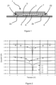
- the photoresistor 1 comprises two electrodes 2a, 2b connected by a photosensitive layer 3 of the photoresistor 1.
- the photosensitive layer 3 is in physical contact with the two electrodes 2a, 2b.
- the two electrodes 2a, 2b can be transparent, for example formed in ITO (acronym for “Indium Tin Oxide”) with a thickness of around 50nm, or can be formed in another material metallic such as gold, silver or nickel, or can be formed into TCO (acronym for “Transparent Conducting Oxide”). transparent conductive) and in this case the thickness of the electrodes can be 100nm.
- the photosensitive layer 3 is preferably formed by a photosensitive organic semiconductor material, for example of the P3HT:PCBM type, the photoresistor 1 is then an organic photoresistor.
- the photosensitive layer 3 advantageously has a thickness of between 300nm and 800nm, and more particularly between 500nm and 700nm.
- the photosensitive layer 3 comprises a first face 4 of which a first zone Z1 is in contact with one of the electrodes 2a and a second zone Z2 is in contact with the other of the electrodes 2b.
- the photosensitive layer 3 has a second face 5 opposite the first face 4. The distance separating the first and second faces 4, 5 gives the thickness of the photosensitive layer 3.
- the second face 5 is preferably the face intended to be oriented towards the light flux.
- P3HT:PCBM is a P-type semiconductor polymer (electron donor) comprising P3HT, an acronym for poly(3-hexylthiophene), or even poly(3-hexylthiophene-2,5-diyl) mixed with an acceptor. Electrons PCBM acronym for methyl [6,6]-phenyl-C61-butanoate.
- the photoresistor 1 comprises two additional layers 6, 7 in contact with the photosensitive layer 3 to have an action on the behavior of the photoresistor with respect to the collection of carriers between the two electrodes 2a, 2b with a view to improve the sensitivity of the photoresistor 1.
- having an action on the behavior of the photoresistor with respect to the collection of carriers between the two electrodes we mean in particular that the additional layers 6, 7 are not interposed between one or the other of the electrodes 2a, 2b and the photosensitive layer 3, and that one face of the additional layer 6, 7 in contact with one of the faces of the photosensitive layer 3 comprises at least one portion which is not located opposite one or the other of the electrodes 2a, 3b. In other words, said portion of the additional layer 6, 7 is not located directly above a carrier injection/or collection face of one or other of the electrodes 2a, 2b in the photosensitive layer. 3.
- a first case it is possible to improve the sensitivity of the photoresistor 1 by making the photosensitive layer 3 less electrically conductive between the two electrodes 2a, 2b.
- the additional layer 6 is preferably a self-assembled monolayer 6 located between the two electrodes 2a, 2b, and configured so as to increase the resistivity of the photosensitive layer 3 at its interface with said self-assembled monolayer. assembly 6 to reduce the dark current of said photoresistor 1.
- the self-assembled monolayer 6 is also known in the field by the acronym SAM for “Self-Assembled monolayer”.
- SAM Self-Assembled monolayer”.
- the self-assembled monolayer 6 makes it possible to modify the resistivity of the channel mentioned previously. More particularly, the self-assembled monolayer 6 is in contact with the first face 4 of the photosensitive layer 3. This self-assembled monolayer 6 can extend between the two electrodes 2a, 2b but is not in contact with the electrodes.
- the self-assembled monolayer is at a distance from the electrodes 2a, 2b.
- the self-assembled monolayer plays the role of a defect between the electrodes 2a, 2b and makes it possible to capture the carriers injected by the electrodes in order to reduce the dark current of the photoresistor.
- the self-assembled monolayer makes it possible to trap the carriers which circulate between the two electrodes 2a, 2b under the photosensitive layer 3.
- the conductivity of the photosensitive layer 3 By conductivity is meant in the present description the electrical conductivity .
- the self-assembled monolayer is of N-type conductivity, in particular in this case the self-assembled monolayer 6 is 4-methoxythiophenol.
- the photosensitive layer 3 is of type N (that is to say of type N conductivity)
- the self-assembled monolayer 6 is of type P conductivity, in particular in this case the self-assembled monolayer 6 is pentafluoro-benzenethiol.
- the photosensitive layer 3 then of type N conduction can be PCNEPV which is the acronym for poly[oxa- 1,4-phenylene-(1-cyano-1,2-vinylene)-(2-methoxy-5-(3,7-dimethyloctyloxy)-1,4-phenylene)-1,2-(2-cyanovinylene)- 1,4-phenylene].
- a self-assembled monolayer can comprise, or be made of, Benzenethiol (whose acronym is BT), or 4-nitrobenzenethiol (whose acronym is NBT), or 4-methylbenzenethiol (whose acronym is MBT), or 4-hydroxybenzenethiol (HBT), or 4-methoxybenzenethiol (whose acronym is MOBT), or 4-fluorobenzenethiol (whose acronym is FBT), or Pentafluorobenzenethiol (whose acronym is PFBT), or 4-chlorobenzenethiol (whose acronym is CBT), or Pentachlorobenzenethiol (whose acronym is PCBT), or 4-bromobenzenethiol (whose acronym is BBT).
- the self-assembled monolayer comprises, or is made of, Benzenethiol (BT), or 4-nitrobenzenethiol (NBT), or 4-methylbenzenethiol (MBT), or 4-hydroxybenzenethiol (HBT), or 4-methoxybenzenethiol (MOBT), it is a self-assembled monolayer of N-type conductivity.
- BT Benzenethiol
- NBT 4-nitrobenzenethiol
- MBT 4-methylbenzenethiol
- HBT 4-hydroxybenzenethiol
- MOBT 4-methoxybenzenethiol
- the self-assembled monolayer comprises, or is made of, 4-fluorobenzenethiol (FBT), or Pentafluorobenzenethiol (PFBT), or 4-chlorobenzenethiol (CBT), or Pentachlorobenzenethiol (PCBT), or 4 -bromobenzenethiol (BBT), it is a self-assembled monolayer of P-type conductivity.
- FBT 4-fluorobenzenethiol
- PFBT Pentafluorobenzenethiol
- CBT 4-chlorobenzenethiol
- PCBT Pentachlorobenzenethiol
- BBT 4 -bromobenzenethiol
- the first case is particularly implemented when the photoresistor 1 is integrated into a detector, a matrix imager or even used alone, in fact in this case the dark current defines the minimum detection threshold of such a detector or imager.
- the additional layer 7 can be a layer of PEDOT:PSS 7 in particular formed on at least part of a front face - the second face 5 mentioned previously - of the photosensitive layer 3 opposite a face rear - the first face 4 mentioned previously - of the photosensitive layer 3 in contact with the electrodes 2a, 2b, and in particular intended to be oriented towards the light flux.
- this layer of PEDOT:PSS 7 is transparent.
- PEDOT:PSS has the advantage of having a higher electrical conductivity than photosensitive layer 3, particularly when the latter is made of P3HT:PCBM.
- the PEDOT:PSS can be generalized to a layer of polymer material having a higher conductivity than the photosensitive layer 3.
- This layer of PEDOT:PSS can have a thickness of the order of a micrometer, and more particularly between 200nm and 500nm.
- the PEDOT:PSS is said to be “floating”, that is to say that it is not used as an electrode, and it allows an improvement in the sensitivity of the photoresistor when the photoresistor is under light in helping in the conduction of photo-generated carriers under light.
- the additional layer 7 is at a distance from the electrodes.
- the first and second cases can be generalized as follows: said at least one additional layer 7 is at a distance from the electrodes: that is to say, it is not in contact with the electrodes.
- PEDOT:PSS poly(3,4-ethylenedioxythiophene) polystyrene sulfonate
- PEDOT poly(3,4-ethylenedioxythiophene) polystyrene sulfonate
- PSS sodium polystyrene sulfonate which is a sulfonated polystyrene.
- the mixture forms a transparent conductive polymer with very good conductivity. It can transport electrons like holes.
- PEDOT:PSS allows, on the one hand, the passage of the luminous flux so that it can generate carriers in the photosensitive layer 3, and on the other hand, to promote the transport of carriers generated in the photosensitive layer 3 to improve their collection and therefore limit their recombination.
- the photoresistor 1 comprises two additional layers 6, 7, one of which is formed by the self-assembled monolayer 6, and the other is formed by the PEDOT:PSS layer 7.
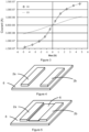
- FIG. 2 is a graph giving the current passing through the photoresistor 1 as a function of the voltage applied to the electrodes 2a, 2b according to four curves C1, C2, C3, C4. These four curves were obtained according to the protocol described previously.
- Curve C1 represents the current as a function of the voltage when the photoresistor 1, devoid of the self-assembled monolayer 6 and the PEDOT:PSS layer, is placed in the dark.
- Curve C2 represents the current versus voltage when the photoresistor 1 comprises the self-assembled monolayer 6 and the PEDOT:PSS layer, and is placed in the dark.
- the curve C3 represents the current as a function of the voltage when the photoresistor 1, devoid of the self-assembled monolayer 6 and the PEDOT:PSS layer, is placed under a calibrated light flux.
- the curve C4 represents the current as a function of the voltage when the photoresistor 1 comprises the self-assembled monolayer 6 and the PEDOT:PSS layer, and is placed under a calibrated light flux. It is thus possible to observe a reduction of the order of a decade on the dark current depending on the implementation or not of the self-assembled monolayer 6 and the PEDOT:PSS layer (curves C1 and C2). It can be seen that the leakage current/dark current is higher without the self-assembled monolayer 6 than with it.
- the self-assembled monolayer 6 acts at its interface with the photosensitive layer 3 as carrier trapping sites.
- the sites polymer tentacles which capture/trap the carriers
- the carrier flux decreases compared to the leakage current if it there is no self-assembled monolayer 6.
- curves C3 and C4 also make it possible to visualize the gain particularly associated with the PEDOT:PSS layer.
- the gain in dark current is explained by the presence of the self-assembled monolayer 6 and the gain in light current is due to PEDOT:PSS 7, each having a different role.
- FIG. 3 illustrates the current flowing through the photoresistor as a function of its bias voltage on a linear scale.
- Curve C5 represents the evolution of the current passing through photoresistor 1 without the PEDOT:PSS 7 layer (and without the self-assembled monolayer) under light as a function of the bias voltage
- curve C6 represents the evolution of the current crossing the photoresistor 1 with the PEDOT:PSS layer 7 (and with the self-assembled monolayer 6) under light as a function of the bias voltage.
- this Figure 3 is a recovery under linear scale of the curves under illuminations (curves C3 to C5 and C4 to C6) of the figure 2 allowing us to show the increase gain under light.
- Curve C6 appears split because a round trip is made on the bias during the experiment.
- For a bias voltage of 5V we note a multiplication of the current passing through photoresistor 1 by three thanks to the use of the PEDOT:PSS 7 layer.
- each layer (the self-assembled monolayer and the PEDOT:PSS layer) intervenes for a given current, the sum is translated through equation 1 which shows that the gain of PEDOT:PSS 7 has more effect on the overall sensitivity than the self-assembled monolayer 6 because the current under light is very high compared to the dark current (the self-assembled monolayer only improves the sensitivity threshold of the photoresistor ).
- the photosensitive layer 3 is sandwiched between the PEDOT:PSS layer 7 and the self-assembled monolayer 6, we then take advantage of the two faces to improve two characteristics of the sensitivity of the photoresistor, namely increasing the current under light and decrease the dark current.
- the photoresistor 1 comprises a substrate 8 on which the electrodes 2a, 2b are arranged as well as the self-assembled monolayer 7 then formed on the substrate 8 in a space located between the electrodes 2a, 2b.
- the invention also relates to a method of manufacturing the photoresistor 1 as described.
- THE figures 4 to 9 illustrate different stages of such a process.
- the elements shown in dotted lines on the figures 6 to 9 are covered elements and not visible from the outside.
- the manufacturing process comprises the following steps: a step of forming two electrodes 2a, 2b of the photoresistor ( figure 4 ) ; a step of forming a photosensitive layer 3 of the photoresistor connecting the two electrodes 2a, 2b ( figures 6 and 8 ) ; a step of forming two additional layers 6, 7 ( Figure 7 ) of the photoresistor 1 intended to be in contact with the photosensitive layer 3 to have an action on the behavior of the photoresistor with respect to the collection of carriers between the two electrodes 2a, 2b in order to improve the sensitivity of the photoresistor 1.
- the step of forming the two electrodes 2a, 2b, preferably transparent, can be carried out by deposition on a suitable substrate 8 ( Figure 4 ).
- the two electrodes 2a, 2b can be deposited by one of the following techniques: screen printing, printing, evaporation by CVD acronym for "Chemical Vapor Deposition” for chemical vapor deposition, evaporation by PVD acronym for “Physical Vapor Deposition” for physical vapor deposition.
- CVD Chemical Vapor Deposition
- PVD Physical Vapor Deposition
- Other techniques for depositing the electrodes 2a, 2b can also be considered by those skilled in the art.
- These electrodes can have a thickness between 20nm and 100nm and preferably equal to 50nm if they are metal electrodes (gold, nickel, silver), or between 70nm and 150nm and preferably equal to 100nm if they are of TCO.
- the substrate 8 can be flexible or rigid, and transparent to light.
- the substrate 8 can be of a type chosen from PEN (acronym for Polyethylene Naphthalate), PET (acronym for Polyethylene Terephthalate), Kapton ® (Polyimide film developed by the company Dupont and corresponding to poly (4,4'-oxydiphenylene -pyromellitimide)), or other.
- the substrate 8 is preferably made of glass or plastic so as to allow the illumination of the photosensitive layer 3 on both sides.
- the electrodes 2a, 2b can be produced in the following manner: the glass or plastic substrate 8 is covered with 125 nm of ITO deposited by sputtering then cleaned by ultrasonic bath successively in the EDI (acronym for de-ionized water), acetone and isopropanol for 10 minutes for each bath. The substrate 8 is then dried under a flow of nitrogen.
- the step of forming the electrodes 2a, 2b then comprises a photo-lithography step carried out to define the pattern of the electrodes 2a, 2b. During this photo-lithography step, photosensitive resin is deposited by spinning on the ITO layer.
- a mask comprising the patterns of the electrodes 2a, 2b is then deposited on the resin which is finally exposed under an ultraviolet lamp.
- the unexposed resin is removed in a chemical bath, and the exposed ITO layer is etched for 5 minutes in a hydrochloric acid bath.
- the exposed resin is then removed in a specific chemical bath.
- the substrate 8 is cleaned again with the same ultrasonic baths to ultimately obtain the two electrodes 2a, 2b formed on the substrate 8.
- the step of forming the additional layer 6 includes the formation, in particular before the step of forming the photosensitive layer 3 ( Figure 6 ), of the self-assembled monolayer 6 between the two electrodes 2a, 2b, in particular such that this self-assembled monolayer 6 is not in contact with the two electrodes 2a, 2b.
- this self-assembled monolayer 6 is deposited on the substrate 8 between the two electrodes 2a, 2b formed on this substrate 8.
- the deposition of this self-assembled monolayer 6 can be done by dipping in a previously prepared solution or by printing . More generally, we say that the step of forming the self-assembled monolayer 6 is a grafting step.
- the self-assembled monolayer 6 has a thickness of the order of the length of the molecules used. In particular, the thickness of the self-assembled monolayer 6 is between 0.5nm and 1nm.
- the step of forming the photosensitive layer 3 is then carried out ( Figure 6 ) by deposition of the latter on the electrodes 2a, 2b and on the self-assembled monolayer 6, in particular such that the latter covers the free parts of the electrodes 2a, 2b and the self-assembled monolayer 6 before its deposition and comes into contact with the substrate 8.
- the step of forming the photosensitive layer 3 is in particular such that after its deposition said photosensitive layer 3 has a thickness of between 300nm and 800nm.
- the photosensitive layer 3 is deposited on the electrodes 2a, 2b, and in particular on the substrate 8 between the two electrodes 2a, 2b ( figure 8 ).
- This photosensitive layer 3 may have the same material or thickness characteristics as in the first case.
- the step of forming the additional layer 7 then consists of depositing on the photosensitive layer 3 a layer of PEDOT:PSS 7 ( Figure 9 ).
- the self-assembled monolayer is not present in the photoresistor 1.
- the photoresistor comprises two additional layers 6, 7. Therefore, after formation of the photosensitive layer 3, the step of forming the additional layer 6 further comprises a step of forming the layer of PEDOT:PSS 7 formed on at least part of a front face of the photosensitive layer 3 ( Figure 7 ) .
- the step of forming the two additional layers comprises the formation of a PEDOT:PSS layer 7 in particular formed on at least part of the front face 5 of the photosensitive layer 3 opposite a rear face of the photosensitive layer 3 in contact with the electrodes 2a, 2b.
- the PEDOT:PSS layer can cover the photosensitive layer 3 up to the substrate of course if it does not create a short circuit between the electrodes.
- the formation of the PEDOT:PSS 7 layer can be carried out by deposition, in particular of the type chosen from: deposition by centrifugal coating, deposition by printing or deposition by screen printing.
- the PEDOT:PSS layer can be deposited by screen printing through a mask, and once the layer 7 has been deposited, the substrate 8 is annealed under a flow of nitrogen at 110°C for 20 minutes to evaporate the water. .
- the PEDOT:PSS used may be that of the company Heraeus:Clevios known under the reference PVPAI4083 ® .
- the photosensitive layer 3 can be formed by preparing a solution of P3HT:PCBM at a total concentration of 50 mg/ml and a ratio polymer (P3HT):fullerene(PCBM) of 1:1 in a chlorobenzene solution. The solution is stirred for 3 hours on a hot plate at 60°C. The material is then deposited by screen printing through a mask previously designed to have the correct dimension of the photoresistor. An annealing for 5 min at 80°C is then carried out to evaporate the solvent. Of course, the deposition of this solution can also be carried out by other techniques such as screen printing, centrifugal coating or printing.
- the photoresistor and the process are linked in such a way that all the characteristics of the photoresistor can be achieved during suitable steps of the process, and that all the structural characteristics described in combination with the process, in particular the thicknesses of the layers and the materials used, can be integrated into the photoresistor.
- the face 5 of the photosensitive layer 3 is the preferred one to orient towards the source of the light flux to be quantified
- the thickness ranges given previously for the electrodes 2a, 2b, the self-assembled monolayer 6, the layer of PEDOT:PSS 7 are in particular such that these elements are transparent to allow illumination of the photoresistor 1 both from its front face located at the level of the PEDOT:PSS 1 layer and from its rear face located at the level of the self-monolayer -assembly 6 or substrate 8 (then also transparent).
- the photoresistor as described can be used to form a light sensor, a detection matrix based on photoresistors or other imager.
- the photosensitive layer 3 does not entirely cover the electrodes, this is intended to leave at the level of each electrode 2a, 2b a contact zone.
Landscapes
- Physics & Mathematics (AREA)
- Electromagnetism (AREA)
- Engineering & Computer Science (AREA)
- Manufacturing & Machinery (AREA)
- Light Receiving Elements (AREA)
- Solid State Image Pick-Up Elements (AREA)
Claims (11)
- Fotowiderstand (1), umfassend zwei Elektroden (2a, 2b), die durch eine fotosensitive Schicht (3) des Fotowiderstands (1) verbunden sind, wobei die fotosensitive Schicht (3) in physischem Kontakt mit den Elektroden (2a, 2b) ist, wobei die fotosensitive Schicht (3) eine erste Seite (4) aufweist und eine zweite Seite (5), die zu der ersten Seite (4) entgegengesetzt ist und dazu bestimmt ist, zu dem Lichtfluss hin ausgerichtet zu sein, dadurch gekennzeichnet, dass der Fotowiderstand (1) zwei zusätzliche Schichten (6, 7) aufweist, die in Kontakt mit der fotosensitiven Schicht (3) sind, um eine Wirkung auf das Verhalten des Fotowiderstands gegenüber dem Sammeln der Ladungsträger zwischen den beiden Elektroden (2a, 2b) zwecks Verbesserung der Empfindlichkeit des Fotowiderstands (1) zu erhalten, wobei die eine dieser zusätzlichen Schichten auf der einen der Seiten (4, 5) der fotosensitiven Schicht (3) gebildet ist und so ausgestaltet ist, dass sie den spezifischen Widerstand der fotosensitiven Schicht (3) an ihrer Grenzfläche zu der zusätzlichen Schicht erhöht, und wobei die andere dieser zusätzlichen Schichten auf der anderen Seite (4, 5) der fotosensitiven Schicht gebildet ist und so ausgestaltet ist, dass sie die Leitfähigkeit der fotosensitiven Schicht (3) mindestens lokal erhöht.
- Fotowiderstand nach dem vorhergehenden Anspruch, dadurch gekennzeichnet, dass die zusätzliche Schicht, die so ausgestaltet ist, dass sie den spezifischen Widerstand der fotosensitiven Schicht (3) erhöht, eine selbstorganisierende Monoschicht (6) ist, die zwischen den beiden Elektroden (2a, 2b) angeordnet ist, um den Dunkelstrom des Fotowiderstands zu reduzieren.
- Fotowiderstand nach dem vorhergehenden Anspruch, dadurch gekennzeichnet, dass die fotosensitive Schicht (3) eine p-Leitfähigkeit hat und dass die selbstorganisierende Monoschicht (6) eine n-Leitfähigkeit hat.
- Fotowiderstand nach Anspruch 2, dadurch gekennzeichnet, dass die fotosensitive Schicht (3) eine n-Leitfähigkeit hat und dass die selbstorganisierende Monoschicht (6) eine p-Leitfähigkeit hat.
- Fotowiderstand nach einem der Ansprüche 2 bis 4, dadurch gekennzeichnet, dass die selbstorganisierende Monoschicht (6) sich zwischen den beiden Elektroden (2a, 2b) erstreckt und nicht mit den Elektroden (2a, 2b) in Kontakt ist.
- Fotowiderstand nach Anspruch 1, dadurch gekennzeichnet, dass die zusätzliche Schicht, die so ausgestaltet ist, dass sie die Leitfähigkeit der fotosensitiven Schicht (3) mindestens lokal erhöht, eine PEDOT:PSS-Schicht (7) ist, die auf mindestens einem Teil einer Vorderseite (5) der fotosensitiven Schicht (3) gebildet ist, die entgegengesetzt zu einer Rückseite (4) der fotosensitiven Schicht (3) ist, die in Kontakt mit den Elektroden (2a, 2b) ist.
- Fotowiderstand nach Anspruch 6, dadurch gekennzeichnet, dass mindestens ein Teil der fotosensitiven Schicht (3) zwischen der PEDOT:PSS-Schicht (7) und der zusätzlichen Schicht, die so ausgestaltet ist, dass sie den spezifischen Widerstand der fotosensitiven Schicht (3) erhöht, sandwichartig aufgenommen ist, wobei diese zusätzliche Schicht (6) eine selbstorganisierende Monoschicht ist.
- Fotowiderstand nach einem der vorhergehenden Ansprüche, dadurch gekennzeichnet, dass die fotosensitive Schicht (3) durch ein fotosensitives organisches Halbleitermaterial gebildet wird.
- Verfahren zur Herstellung eines Fotowiderstands (1) nach einem der vorhergehenden Ansprüche, dadurch gekennzeichnet, dass es umfasst:• einen Schritt des Bildens von zwei Elektroden (2a, 2b) des Fotowiderstands (1),• einen Schritt des Bildens einer fotosensitiven Schicht (3) des Fotowiderstands (1), die die beiden Elektroden (2a, 2b) verbindet und in physischem Kontakt mit den beiden Elektroden ist, wobei die fotosensitive Schicht (3) eine erste Seite (4) aufweist und eine zweite Seite (5), die zu der ersten Seite (4) entgegengesetzt ist und dazu bestimmt ist, zu dem Lichtfluss hin ausgerichtet zu sein,• einen Schritt des Bildens von zwei zusätzlichen Schichten (6, 7) des Fotowiderstands (1), die dazu bestimmt sind, in Kontakt mit der fotosensitiven Schicht (3) zu sein, um eine Wirkung auf das Verhalten des Fotowiderstands gegenüber dem Sammeln der Ladungsträger zwischen den beiden Elektroden (2a, 2b) zwecks Verbesserung der Empfindlichkeit des Fotowiderstands (1) zu erhalten, wobei die eine dieser zusätzlichen Schichten auf der einen der Seiten (4, 5) der fotosensitiven Schicht (3) gebildet ist und so ausgestaltet ist, dass sie den spezifischen Widerstand der fotosensitiven Schicht (3) an ihrer Grenzfläche zu der zusätzlichen Schicht erhöht, und wobei die andere dieser zusätzlichen Schichten auf der anderen Seite (4, 5) der fotosensitiven Schicht gebildet ist und so ausgestaltet ist, dass sie die Leitfähigkeit der fotosensitiven Schicht (3) mindestens lokal erhöht.
- Fotowiderstand nach Anspruch 9, dadurch gekennzeichnet, dass der Schritt des Bildens der zusätzlichen Schicht, die so ausgestaltet ist, dass sie den spezifischen Widerstand der fotosensitiven Schicht (3) erhöht, das Bilden einer selbstorganisierenden Monoschicht (6) zwischen den beiden Elektroden (2a, 2b) umfasst.
- Verfahren nach einem der Ansprüche 9 bis 10, dadurch gekennzeichnet, dass der Schritt des Bildens der zusätzlichen Schicht, die so ausgestaltet ist, dass sie die Leitfähigkeit der fotosensitiven Schicht (3) mindestens lokal erhöht, das Bilden einer PEDOT:PSS-Schicht (7) umfasst, die auf mindestens einem Teil einer Vorderseite (5) der fotosensitiven Schicht (3) gebildet ist, die entgegengesetzt zu einer Rückseite der fotosensitiven Schicht (3) ist, die in Kontakt mit den Elektroden (2a, 2b) ist.
Applications Claiming Priority (2)
| Application Number | Priority Date | Filing Date | Title |
|---|---|---|---|
| FR1650048A FR3046496B1 (fr) | 2016-01-05 | 2016-01-05 | Photoresistance a sensibilite amelioree |
| PCT/FR2017/050001 WO2017118805A1 (fr) | 2016-01-05 | 2017-01-02 | Photorésistance à sensibilité améliorée |
Publications (2)
| Publication Number | Publication Date |
|---|---|
| EP3400618A1 EP3400618A1 (de) | 2018-11-14 |
| EP3400618B1 true EP3400618B1 (de) | 2023-12-13 |
Family
ID=55806521
Family Applications (1)
| Application Number | Title | Priority Date | Filing Date |
|---|---|---|---|
| EP17702417.1A Active EP3400618B1 (de) | 2016-01-05 | 2017-01-02 | Fotowiderstand mit verbesserter empfindlichkeit |
Country Status (4)
| Country | Link |
|---|---|
| US (1) | US10944066B2 (de) |
| EP (1) | EP3400618B1 (de) |
| FR (1) | FR3046496B1 (de) |
| WO (1) | WO2017118805A1 (de) |
Families Citing this family (2)
| Publication number | Priority date | Publication date | Assignee | Title |
|---|---|---|---|---|
| FR3098821B1 (fr) | 2019-07-19 | 2023-05-26 | Isorg | Encre pour une couche d’injection d’électrons |
| KR102705350B1 (ko) * | 2019-10-15 | 2024-09-12 | 삼성디스플레이 주식회사 | 표시 장치 및 그 제조 방법 |
Family Cites Families (9)
| Publication number | Priority date | Publication date | Assignee | Title |
|---|---|---|---|---|
| GB0309355D0 (en) * | 2003-04-24 | 2003-06-04 | Univ Cambridge Tech | Organic electronic devices incorporating semiconducting polymer |
| US8247801B2 (en) * | 2006-03-31 | 2012-08-21 | Imec | Organic semi-conductor photo-detecting device |
| CN100555702C (zh) * | 2006-04-29 | 2009-10-28 | 中国科学院长春应用化学研究所 | 有机半导体晶体薄膜及弱取向外延生长制备方法和应用 |
| DE102007046444A1 (de) * | 2007-09-28 | 2009-04-02 | Siemens Ag | Organischer Photodetektor mit reduziertem Dunkelstrom |
| ES2384766B1 (es) * | 2010-12-10 | 2013-05-22 | Fundación Imdea Nanociencia | Fotodetector sensible a la posición, procedimiento de obtención del mismo y procedimiento de medida de la respuesta del fotodetector. |
| DE102011077961A1 (de) * | 2011-06-22 | 2012-12-27 | Siemens Aktiengesellschaft | Schwachlichtdetektion mit organischem fotosensitivem Bauteil |
| FR2977080B1 (fr) * | 2011-06-22 | 2014-01-10 | Commissariat Energie Atomique | Photodiode organique dotee d'une zone active comportant des moyens pour favoriser la collecte et la conduction des porteurs de charge |
| US9837611B2 (en) * | 2011-09-23 | 2017-12-05 | Board Of Regents, The University Of Texas System | Photo-switchable fullerene-based materials as interfacial layers in organic photovoltaics |
| WO2014104976A1 (en) * | 2012-12-26 | 2014-07-03 | Agency For Science, Technology And Research | Organic electronic devices |
-
2016
- 2016-01-05 FR FR1650048A patent/FR3046496B1/fr not_active Expired - Fee Related
-
2017
- 2017-01-02 EP EP17702417.1A patent/EP3400618B1/de active Active
- 2017-01-02 US US16/067,942 patent/US10944066B2/en active Active
- 2017-01-02 WO PCT/FR2017/050001 patent/WO2017118805A1/fr not_active Ceased
Also Published As
| Publication number | Publication date |
|---|---|
| FR3046496A1 (fr) | 2017-07-07 |
| FR3046496B1 (fr) | 2018-04-27 |
| WO2017118805A1 (fr) | 2017-07-13 |
| EP3400618A1 (de) | 2018-11-14 |
| US20200052232A1 (en) | 2020-02-13 |
| US10944066B2 (en) | 2021-03-09 |
Similar Documents
| Publication | Publication Date | Title |
|---|---|---|
| WO2013007753A1 (fr) | Matrice de photodiodes ingaas | |
| JP2014120616A (ja) | 有機光電変換素子、それを備えた積層型有機撮像素子及び積層型有機太陽電池、並びに有機光電変換素子の製造方法 | |
| EP3767679A1 (de) | Pixel eines bildsensors | |
| FR3023067A1 (fr) | Cellules tandem multifils | |
| FR2938374A1 (fr) | Photodetecteur a gain interne et detecteur comportant une matrice de tels photodetecteurs | |
| EP3613080A1 (de) | Strahlungsdetektionsvorrichtung, organische fotodioden umfassend | |
| Shan et al. | Self‐Assembled Monolayer Assisted Biphasic Heterojunction Organic Photodiode for Panel‐Level Manufacturing of Active‐Matrix Optical Imager | |
| WO2015033291A1 (fr) | Module photovoltaique semi-transparent et procédé d'obtention correspondant | |
| EP3400618A1 (de) | Fotowiderstand mit verbesserter empfindlichkeit | |
| EP1903612A1 (de) | Fotodiode mit Lawine | |
| EP3140867B1 (de) | Matrixdetektor mit einem metallgitter in einer detektionsschicht und herstellungsverfahren | |
| FR3059827A1 (fr) | Composant optoelectronique a absorption amelioree | |
| FR3093233A1 (fr) | Dispositif matriciel pour capteur d'image, à transistors en couches minces et photodiodes organiques | |
| FR3046300A1 (fr) | Dispositif optoelectronique organique, matrice de tels dispositifs et procede de fabrication de telles matrices. | |
| Troughton et al. | Efficient Hybrid Amorphous Silicon/Organic Tandem Solar Cells Enabled by Near‐Infrared Absorbing Nonfullerene Acceptors | |
| EP3111480B1 (de) | Elektronische vorrichtung mit organischer optoelektronischer komponente und zwei organischen transistoren | |
| EP3031087B1 (de) | Verfahren zur herstellung einer organischen cmos-schaltung und organische cmos-schaltung mit schutz vor uv-strahlung | |
| EP3552243B1 (de) | Lichtdetektor mit ladungsträgersammelschicht mit funktionalisierten nanodrähten | |
| FR3049390A1 (fr) | Photodetecteur a sensibilite amelioree par adjonction d’un materiau photoluminescent au sein du materiau photosensible | |
| WO2014013183A1 (fr) | Electrode supportee transparente pour oled | |
| WO2015189494A1 (fr) | Dispositif électronique organique et son procédé de préparation | |
| FR2911007A1 (fr) | Capteur d'image comprenant des pixels a un transistor | |
| FR2919428A1 (fr) | Electrode de composant optoelectronique,comprenant au moins une couche d'un oxyde transparent revetue d'une couche metallique,et composant optoelectronique correspondant. | |
| CN111312836B (zh) | 光电探测器 | |
| FR3117268A1 (fr) | Pixel d'un capteur de lumière et son procédé de fabrication |
Legal Events
| Date | Code | Title | Description |
|---|---|---|---|
| STAA | Information on the status of an ep patent application or granted ep patent |
Free format text: STATUS: UNKNOWN |
|
| STAA | Information on the status of an ep patent application or granted ep patent |
Free format text: STATUS: THE INTERNATIONAL PUBLICATION HAS BEEN MADE |
|
| PUAI | Public reference made under article 153(3) epc to a published international application that has entered the european phase |
Free format text: ORIGINAL CODE: 0009012 |
|
| STAA | Information on the status of an ep patent application or granted ep patent |
Free format text: STATUS: REQUEST FOR EXAMINATION WAS MADE |
|
| 17P | Request for examination filed |
Effective date: 20180702 |
|
| AK | Designated contracting states |
Kind code of ref document: A1 Designated state(s): AL AT BE BG CH CY CZ DE DK EE ES FI FR GB GR HR HU IE IS IT LI LT LU LV MC MK MT NL NO PL PT RO RS SE SI SK SM TR |
|
| AX | Request for extension of the european patent |
Extension state: BA ME |
|
| DAV | Request for validation of the european patent (deleted) | ||
| DAX | Request for extension of the european patent (deleted) | ||
| STAA | Information on the status of an ep patent application or granted ep patent |
Free format text: STATUS: EXAMINATION IS IN PROGRESS |
|
| 17Q | First examination report despatched |
Effective date: 20210430 |
|
| REG | Reference to a national code |
Ref country code: DE Free format text: PREVIOUS MAIN CLASS: H01L0051050000 Ref country code: DE Ref legal event code: R079 Ref document number: 602017077437 Country of ref document: DE Free format text: PREVIOUS MAIN CLASS: H01L0051050000 Ipc: H10K0030000000 |
|
| GRAP | Despatch of communication of intention to grant a patent |
Free format text: ORIGINAL CODE: EPIDOSNIGR1 |
|
| STAA | Information on the status of an ep patent application or granted ep patent |
Free format text: STATUS: GRANT OF PATENT IS INTENDED |
|
| RIC1 | Information provided on ipc code assigned before grant |
Ipc: H10K 30/84 20230101ALI20230616BHEP Ipc: H10K 30/00 20230101AFI20230616BHEP |
|
| INTG | Intention to grant announced |
Effective date: 20230705 |
|
| GRAS | Grant fee paid |
Free format text: ORIGINAL CODE: EPIDOSNIGR3 |
|
| GRAA | (expected) grant |
Free format text: ORIGINAL CODE: 0009210 |
|
| STAA | Information on the status of an ep patent application or granted ep patent |
Free format text: STATUS: THE PATENT HAS BEEN GRANTED |
|
| AK | Designated contracting states |
Kind code of ref document: B1 Designated state(s): AL AT BE BG CH CY CZ DE DK EE ES FI FR GB GR HR HU IE IS IT LI LT LU LV MC MK MT NL NO PL PT RO RS SE SI SK SM TR |
|
| REG | Reference to a national code |
Ref country code: GB Ref legal event code: FG4D Free format text: NOT ENGLISH |
|
| REG | Reference to a national code |
Ref country code: CH Ref legal event code: EP |
|
| REG | Reference to a national code |
Ref country code: DE Ref legal event code: R096 Ref document number: 602017077437 Country of ref document: DE |
|
| REG | Reference to a national code |
Ref country code: IE Ref legal event code: FG4D Free format text: LANGUAGE OF EP DOCUMENT: FRENCH |
|
| PG25 | Lapsed in a contracting state [announced via postgrant information from national office to epo] |
Ref country code: GR Free format text: LAPSE BECAUSE OF FAILURE TO SUBMIT A TRANSLATION OF THE DESCRIPTION OR TO PAY THE FEE WITHIN THE PRESCRIBED TIME-LIMIT Effective date: 20240314 |
|
| REG | Reference to a national code |
Ref country code: LT Ref legal event code: MG9D |
|
| PG25 | Lapsed in a contracting state [announced via postgrant information from national office to epo] |
Ref country code: LT Free format text: LAPSE BECAUSE OF FAILURE TO SUBMIT A TRANSLATION OF THE DESCRIPTION OR TO PAY THE FEE WITHIN THE PRESCRIBED TIME-LIMIT Effective date: 20231213 |
|
| REG | Reference to a national code |
Ref country code: NL Ref legal event code: MP Effective date: 20231213 |
|
| PG25 | Lapsed in a contracting state [announced via postgrant information from national office to epo] |
Ref country code: ES Free format text: LAPSE BECAUSE OF FAILURE TO SUBMIT A TRANSLATION OF THE DESCRIPTION OR TO PAY THE FEE WITHIN THE PRESCRIBED TIME-LIMIT Effective date: 20231213 |
|
| PG25 | Lapsed in a contracting state [announced via postgrant information from national office to epo] |
Ref country code: LT Free format text: LAPSE BECAUSE OF FAILURE TO SUBMIT A TRANSLATION OF THE DESCRIPTION OR TO PAY THE FEE WITHIN THE PRESCRIBED TIME-LIMIT Effective date: 20231213 Ref country code: GR Free format text: LAPSE BECAUSE OF FAILURE TO SUBMIT A TRANSLATION OF THE DESCRIPTION OR TO PAY THE FEE WITHIN THE PRESCRIBED TIME-LIMIT Effective date: 20240314 Ref country code: ES Free format text: LAPSE BECAUSE OF FAILURE TO SUBMIT A TRANSLATION OF THE DESCRIPTION OR TO PAY THE FEE WITHIN THE PRESCRIBED TIME-LIMIT Effective date: 20231213 Ref country code: BG Free format text: LAPSE BECAUSE OF FAILURE TO SUBMIT A TRANSLATION OF THE DESCRIPTION OR TO PAY THE FEE WITHIN THE PRESCRIBED TIME-LIMIT Effective date: 20240313 |
|
| REG | Reference to a national code |
Ref country code: AT Ref legal event code: MK05 Ref document number: 1641609 Country of ref document: AT Kind code of ref document: T Effective date: 20231213 |
|
| PG25 | Lapsed in a contracting state [announced via postgrant information from national office to epo] |
Ref country code: NL Free format text: LAPSE BECAUSE OF FAILURE TO SUBMIT A TRANSLATION OF THE DESCRIPTION OR TO PAY THE FEE WITHIN THE PRESCRIBED TIME-LIMIT Effective date: 20231213 |
|
| PG25 | Lapsed in a contracting state [announced via postgrant information from national office to epo] |
Ref country code: SE Free format text: LAPSE BECAUSE OF FAILURE TO SUBMIT A TRANSLATION OF THE DESCRIPTION OR TO PAY THE FEE WITHIN THE PRESCRIBED TIME-LIMIT Effective date: 20231213 Ref country code: RS Free format text: LAPSE BECAUSE OF FAILURE TO SUBMIT A TRANSLATION OF THE DESCRIPTION OR TO PAY THE FEE WITHIN THE PRESCRIBED TIME-LIMIT Effective date: 20231213 Ref country code: NO Free format text: LAPSE BECAUSE OF FAILURE TO SUBMIT A TRANSLATION OF THE DESCRIPTION OR TO PAY THE FEE WITHIN THE PRESCRIBED TIME-LIMIT Effective date: 20240313 Ref country code: NL Free format text: LAPSE BECAUSE OF FAILURE TO SUBMIT A TRANSLATION OF THE DESCRIPTION OR TO PAY THE FEE WITHIN THE PRESCRIBED TIME-LIMIT Effective date: 20231213 Ref country code: LV Free format text: LAPSE BECAUSE OF FAILURE TO SUBMIT A TRANSLATION OF THE DESCRIPTION OR TO PAY THE FEE WITHIN THE PRESCRIBED TIME-LIMIT Effective date: 20231213 Ref country code: HR Free format text: LAPSE BECAUSE OF FAILURE TO SUBMIT A TRANSLATION OF THE DESCRIPTION OR TO PAY THE FEE WITHIN THE PRESCRIBED TIME-LIMIT Effective date: 20231213 |
|
| PG25 | Lapsed in a contracting state [announced via postgrant information from national office to epo] |
Ref country code: IS Free format text: LAPSE BECAUSE OF FAILURE TO SUBMIT A TRANSLATION OF THE DESCRIPTION OR TO PAY THE FEE WITHIN THE PRESCRIBED TIME-LIMIT Effective date: 20240413 |
|
| PG25 | Lapsed in a contracting state [announced via postgrant information from national office to epo] |
Ref country code: CZ Free format text: LAPSE BECAUSE OF FAILURE TO SUBMIT A TRANSLATION OF THE DESCRIPTION OR TO PAY THE FEE WITHIN THE PRESCRIBED TIME-LIMIT Effective date: 20231213 Ref country code: AT Free format text: LAPSE BECAUSE OF FAILURE TO SUBMIT A TRANSLATION OF THE DESCRIPTION OR TO PAY THE FEE WITHIN THE PRESCRIBED TIME-LIMIT Effective date: 20231213 |
|
| PG25 | Lapsed in a contracting state [announced via postgrant information from national office to epo] |
Ref country code: SK Free format text: LAPSE BECAUSE OF FAILURE TO SUBMIT A TRANSLATION OF THE DESCRIPTION OR TO PAY THE FEE WITHIN THE PRESCRIBED TIME-LIMIT Effective date: 20231213 |
|
| PG25 | Lapsed in a contracting state [announced via postgrant information from national office to epo] |
Ref country code: SM Free format text: LAPSE BECAUSE OF FAILURE TO SUBMIT A TRANSLATION OF THE DESCRIPTION OR TO PAY THE FEE WITHIN THE PRESCRIBED TIME-LIMIT Effective date: 20231213 Ref country code: SK Free format text: LAPSE BECAUSE OF FAILURE TO SUBMIT A TRANSLATION OF THE DESCRIPTION OR TO PAY THE FEE WITHIN THE PRESCRIBED TIME-LIMIT Effective date: 20231213 Ref country code: RO Free format text: LAPSE BECAUSE OF FAILURE TO SUBMIT A TRANSLATION OF THE DESCRIPTION OR TO PAY THE FEE WITHIN THE PRESCRIBED TIME-LIMIT Effective date: 20231213 Ref country code: IT Free format text: LAPSE BECAUSE OF FAILURE TO SUBMIT A TRANSLATION OF THE DESCRIPTION OR TO PAY THE FEE WITHIN THE PRESCRIBED TIME-LIMIT Effective date: 20231213 Ref country code: IS Free format text: LAPSE BECAUSE OF FAILURE TO SUBMIT A TRANSLATION OF THE DESCRIPTION OR TO PAY THE FEE WITHIN THE PRESCRIBED TIME-LIMIT Effective date: 20240413 Ref country code: EE Free format text: LAPSE BECAUSE OF FAILURE TO SUBMIT A TRANSLATION OF THE DESCRIPTION OR TO PAY THE FEE WITHIN THE PRESCRIBED TIME-LIMIT Effective date: 20231213 Ref country code: CZ Free format text: LAPSE BECAUSE OF FAILURE TO SUBMIT A TRANSLATION OF THE DESCRIPTION OR TO PAY THE FEE WITHIN THE PRESCRIBED TIME-LIMIT Effective date: 20231213 Ref country code: AT Free format text: LAPSE BECAUSE OF FAILURE TO SUBMIT A TRANSLATION OF THE DESCRIPTION OR TO PAY THE FEE WITHIN THE PRESCRIBED TIME-LIMIT Effective date: 20231213 |
|
| PG25 | Lapsed in a contracting state [announced via postgrant information from national office to epo] |
Ref country code: PL Free format text: LAPSE BECAUSE OF FAILURE TO SUBMIT A TRANSLATION OF THE DESCRIPTION OR TO PAY THE FEE WITHIN THE PRESCRIBED TIME-LIMIT Effective date: 20231213 Ref country code: PT Free format text: LAPSE BECAUSE OF FAILURE TO SUBMIT A TRANSLATION OF THE DESCRIPTION OR TO PAY THE FEE WITHIN THE PRESCRIBED TIME-LIMIT Effective date: 20240415 |
|
| PG25 | Lapsed in a contracting state [announced via postgrant information from national office to epo] |
Ref country code: PT Free format text: LAPSE BECAUSE OF FAILURE TO SUBMIT A TRANSLATION OF THE DESCRIPTION OR TO PAY THE FEE WITHIN THE PRESCRIBED TIME-LIMIT Effective date: 20240415 Ref country code: PL Free format text: LAPSE BECAUSE OF FAILURE TO SUBMIT A TRANSLATION OF THE DESCRIPTION OR TO PAY THE FEE WITHIN THE PRESCRIBED TIME-LIMIT Effective date: 20231213 |
|
| REG | Reference to a national code |
Ref country code: CH Ref legal event code: PL |
|
| PG25 | Lapsed in a contracting state [announced via postgrant information from national office to epo] |
Ref country code: LU Free format text: LAPSE BECAUSE OF NON-PAYMENT OF DUE FEES Effective date: 20240102 |
|
| REG | Reference to a national code |
Ref country code: DE Ref legal event code: R097 Ref document number: 602017077437 Country of ref document: DE |
|
| PG25 | Lapsed in a contracting state [announced via postgrant information from national office to epo] |
Ref country code: LU Free format text: LAPSE BECAUSE OF NON-PAYMENT OF DUE FEES Effective date: 20240102 Ref country code: MC Free format text: LAPSE BECAUSE OF FAILURE TO SUBMIT A TRANSLATION OF THE DESCRIPTION OR TO PAY THE FEE WITHIN THE PRESCRIBED TIME-LIMIT Effective date: 20231213 |
|
| PG25 | Lapsed in a contracting state [announced via postgrant information from national office to epo] |
Ref country code: DK Free format text: LAPSE BECAUSE OF FAILURE TO SUBMIT A TRANSLATION OF THE DESCRIPTION OR TO PAY THE FEE WITHIN THE PRESCRIBED TIME-LIMIT Effective date: 20231213 |
|
| PG25 | Lapsed in a contracting state [announced via postgrant information from national office to epo] |
Ref country code: BE Free format text: LAPSE BECAUSE OF NON-PAYMENT OF DUE FEES Effective date: 20240131 |
|
| PLBE | No opposition filed within time limit |
Free format text: ORIGINAL CODE: 0009261 |
|
| STAA | Information on the status of an ep patent application or granted ep patent |
Free format text: STATUS: NO OPPOSITION FILED WITHIN TIME LIMIT |
|
| PG25 | Lapsed in a contracting state [announced via postgrant information from national office to epo] |
Ref country code: CH Free format text: LAPSE BECAUSE OF NON-PAYMENT OF DUE FEES Effective date: 20240131 |
|
| PG25 | Lapsed in a contracting state [announced via postgrant information from national office to epo] |
Ref country code: SI Free format text: LAPSE BECAUSE OF FAILURE TO SUBMIT A TRANSLATION OF THE DESCRIPTION OR TO PAY THE FEE WITHIN THE PRESCRIBED TIME-LIMIT Effective date: 20231213 |
|
| RAP4 | Party data changed (patent owner data changed or rights of a patent transferred) |
Owner name: ISORG Owner name: COMMISSARIAT A L'ENERGIE ATOMIQUE ET AUX ENERGIESALTERNATIVES |
|
| PG25 | Lapsed in a contracting state [announced via postgrant information from national office to epo] |
Ref country code: SI Free format text: LAPSE BECAUSE OF FAILURE TO SUBMIT A TRANSLATION OF THE DESCRIPTION OR TO PAY THE FEE WITHIN THE PRESCRIBED TIME-LIMIT Effective date: 20231213 Ref country code: DK Free format text: LAPSE BECAUSE OF FAILURE TO SUBMIT A TRANSLATION OF THE DESCRIPTION OR TO PAY THE FEE WITHIN THE PRESCRIBED TIME-LIMIT Effective date: 20231213 Ref country code: CH Free format text: LAPSE BECAUSE OF NON-PAYMENT OF DUE FEES Effective date: 20240131 Ref country code: BE Free format text: LAPSE BECAUSE OF NON-PAYMENT OF DUE FEES Effective date: 20240131 |
|
| REG | Reference to a national code |
Ref country code: BE Ref legal event code: MM Effective date: 20240131 |
|
| 26N | No opposition filed |
Effective date: 20240916 |
|
| PG25 | Lapsed in a contracting state [announced via postgrant information from national office to epo] |
Ref country code: IE Free format text: LAPSE BECAUSE OF NON-PAYMENT OF DUE FEES Effective date: 20240102 |
|
| PG25 | Lapsed in a contracting state [announced via postgrant information from national office to epo] |
Ref country code: IE Free format text: LAPSE BECAUSE OF NON-PAYMENT OF DUE FEES Effective date: 20240102 |
|
| PGFP | Annual fee paid to national office [announced via postgrant information from national office to epo] |
Ref country code: DE Payment date: 20250120 Year of fee payment: 9 |
|
| PGFP | Annual fee paid to national office [announced via postgrant information from national office to epo] |
Ref country code: FR Payment date: 20250122 Year of fee payment: 9 |
|
| PGFP | Annual fee paid to national office [announced via postgrant information from national office to epo] |
Ref country code: GB Payment date: 20250122 Year of fee payment: 9 |
|
| PG25 | Lapsed in a contracting state [announced via postgrant information from national office to epo] |
Ref country code: CY Free format text: LAPSE BECAUSE OF FAILURE TO SUBMIT A TRANSLATION OF THE DESCRIPTION OR TO PAY THE FEE WITHIN THE PRESCRIBED TIME-LIMIT; INVALID AB INITIO Effective date: 20170102 |
|
| PG25 | Lapsed in a contracting state [announced via postgrant information from national office to epo] |
Ref country code: HU Free format text: LAPSE BECAUSE OF FAILURE TO SUBMIT A TRANSLATION OF THE DESCRIPTION OR TO PAY THE FEE WITHIN THE PRESCRIBED TIME-LIMIT; INVALID AB INITIO Effective date: 20170102 |
|
| PG25 | Lapsed in a contracting state [announced via postgrant information from national office to epo] |
Ref country code: FI Free format text: LAPSE BECAUSE OF FAILURE TO SUBMIT A TRANSLATION OF THE DESCRIPTION OR TO PAY THE FEE WITHIN THE PRESCRIBED TIME-LIMIT Effective date: 20231213 |
|
| PG25 | Lapsed in a contracting state [announced via postgrant information from national office to epo] |
Ref country code: TR Free format text: LAPSE BECAUSE OF FAILURE TO SUBMIT A TRANSLATION OF THE DESCRIPTION OR TO PAY THE FEE WITHIN THE PRESCRIBED TIME-LIMIT Effective date: 20231213 |