EP3396842A1 - Bidirectional conversion circuit and bidirectional converter - Google Patents
Bidirectional conversion circuit and bidirectional converter Download PDFInfo
- Publication number
- EP3396842A1 EP3396842A1 EP16877576.5A EP16877576A EP3396842A1 EP 3396842 A1 EP3396842 A1 EP 3396842A1 EP 16877576 A EP16877576 A EP 16877576A EP 3396842 A1 EP3396842 A1 EP 3396842A1
- Authority
- EP
- European Patent Office
- Prior art keywords
- bidirectional
- time
- diode
- conversion circuit
- switching transistor
- Prior art date
- Legal status (The legal status is an assumption and is not a legal conclusion. Google has not performed a legal analysis and makes no representation as to the accuracy of the status listed.)
- Pending
Links
Images



Classifications
-
- H—ELECTRICITY
- H02—GENERATION; CONVERSION OR DISTRIBUTION OF ELECTRIC POWER
- H02M—APPARATUS FOR CONVERSION BETWEEN AC AND AC, BETWEEN AC AND DC, OR BETWEEN DC AND DC, AND FOR USE WITH MAINS OR SIMILAR POWER SUPPLY SYSTEMS; CONVERSION OF DC OR AC INPUT POWER INTO SURGE OUTPUT POWER; CONTROL OR REGULATION THEREOF
- H02M7/00—Conversion of AC power input into DC power output; Conversion of DC power input into AC power output
- H02M7/42—Conversion of DC power input into AC power output without possibility of reversal
- H02M7/44—Conversion of DC power input into AC power output without possibility of reversal by static converters
- H02M7/48—Conversion of DC power input into AC power output without possibility of reversal by static converters using discharge tubes with control electrode or semiconductor devices with control electrode
- H02M7/53—Conversion of DC power input into AC power output without possibility of reversal by static converters using discharge tubes with control electrode or semiconductor devices with control electrode using devices of a triode or transistor type requiring continuous application of a control signal
- H02M7/537—Conversion of DC power input into AC power output without possibility of reversal by static converters using discharge tubes with control electrode or semiconductor devices with control electrode using devices of a triode or transistor type requiring continuous application of a control signal using semiconductor devices only, e.g. single switched pulse inverters
- H02M7/5387—Conversion of DC power input into AC power output without possibility of reversal by static converters using discharge tubes with control electrode or semiconductor devices with control electrode using devices of a triode or transistor type requiring continuous application of a control signal using semiconductor devices only, e.g. single switched pulse inverters in a bridge configuration
-
- H—ELECTRICITY
- H02—GENERATION; CONVERSION OR DISTRIBUTION OF ELECTRIC POWER
- H02M—APPARATUS FOR CONVERSION BETWEEN AC AND AC, BETWEEN AC AND DC, OR BETWEEN DC AND DC, AND FOR USE WITH MAINS OR SIMILAR POWER SUPPLY SYSTEMS; CONVERSION OF DC OR AC INPUT POWER INTO SURGE OUTPUT POWER; CONTROL OR REGULATION THEREOF
- H02M7/00—Conversion of AC power input into DC power output; Conversion of DC power input into AC power output
- H02M7/66—Conversion of AC power input into DC power output; Conversion of DC power input into AC power output with possibility of reversal
- H02M7/68—Conversion of AC power input into DC power output; Conversion of DC power input into AC power output with possibility of reversal by static converters
- H02M7/72—Conversion of AC power input into DC power output; Conversion of DC power input into AC power output with possibility of reversal by static converters using discharge tubes with control electrode or semiconductor devices with control electrode
- H02M7/79—Conversion of AC power input into DC power output; Conversion of DC power input into AC power output with possibility of reversal by static converters using discharge tubes with control electrode or semiconductor devices with control electrode using devices of a triode or transistor type requiring continuous application of a control signal
- H02M7/797—Conversion of AC power input into DC power output; Conversion of DC power input into AC power output with possibility of reversal by static converters using discharge tubes with control electrode or semiconductor devices with control electrode using devices of a triode or transistor type requiring continuous application of a control signal using semiconductor devices only
-
- H—ELECTRICITY
- H02—GENERATION; CONVERSION OR DISTRIBUTION OF ELECTRIC POWER
- H02M—APPARATUS FOR CONVERSION BETWEEN AC AND AC, BETWEEN AC AND DC, OR BETWEEN DC AND DC, AND FOR USE WITH MAINS OR SIMILAR POWER SUPPLY SYSTEMS; CONVERSION OF DC OR AC INPUT POWER INTO SURGE OUTPUT POWER; CONTROL OR REGULATION THEREOF
- H02M1/00—Details of apparatus for conversion
- H02M1/0003—Details of control, feedback or regulation circuits
-
- H—ELECTRICITY
- H02—GENERATION; CONVERSION OR DISTRIBUTION OF ELECTRIC POWER
- H02M—APPARATUS FOR CONVERSION BETWEEN AC AND AC, BETWEEN AC AND DC, OR BETWEEN DC AND DC, AND FOR USE WITH MAINS OR SIMILAR POWER SUPPLY SYSTEMS; CONVERSION OF DC OR AC INPUT POWER INTO SURGE OUTPUT POWER; CONTROL OR REGULATION THEREOF
- H02M1/00—Details of apparatus for conversion
- H02M1/38—Means for preventing simultaneous conduction of switches
-
- H—ELECTRICITY
- H02—GENERATION; CONVERSION OR DISTRIBUTION OF ELECTRIC POWER
- H02M—APPARATUS FOR CONVERSION BETWEEN AC AND AC, BETWEEN AC AND DC, OR BETWEEN DC AND DC, AND FOR USE WITH MAINS OR SIMILAR POWER SUPPLY SYSTEMS; CONVERSION OF DC OR AC INPUT POWER INTO SURGE OUTPUT POWER; CONTROL OR REGULATION THEREOF
- H02M1/00—Details of apparatus for conversion
- H02M1/42—Circuits or arrangements for compensating for or adjusting power factor in converters or inverters
-
- H—ELECTRICITY
- H02—GENERATION; CONVERSION OR DISTRIBUTION OF ELECTRIC POWER
- H02M—APPARATUS FOR CONVERSION BETWEEN AC AND AC, BETWEEN AC AND DC, OR BETWEEN DC AND DC, AND FOR USE WITH MAINS OR SIMILAR POWER SUPPLY SYSTEMS; CONVERSION OF DC OR AC INPUT POWER INTO SURGE OUTPUT POWER; CONTROL OR REGULATION THEREOF
- H02M7/00—Conversion of AC power input into DC power output; Conversion of DC power input into AC power output
- H02M7/42—Conversion of DC power input into AC power output without possibility of reversal
- H02M7/44—Conversion of DC power input into AC power output without possibility of reversal by static converters
- H02M7/48—Conversion of DC power input into AC power output without possibility of reversal by static converters using discharge tubes with control electrode or semiconductor devices with control electrode
- H02M7/53—Conversion of DC power input into AC power output without possibility of reversal by static converters using discharge tubes with control electrode or semiconductor devices with control electrode using devices of a triode or transistor type requiring continuous application of a control signal
- H02M7/537—Conversion of DC power input into AC power output without possibility of reversal by static converters using discharge tubes with control electrode or semiconductor devices with control electrode using devices of a triode or transistor type requiring continuous application of a control signal using semiconductor devices only, e.g. single switched pulse inverters
- H02M7/5387—Conversion of DC power input into AC power output without possibility of reversal by static converters using discharge tubes with control electrode or semiconductor devices with control electrode using devices of a triode or transistor type requiring continuous application of a control signal using semiconductor devices only, e.g. single switched pulse inverters in a bridge configuration
- H02M7/5388—Conversion of DC power input into AC power output without possibility of reversal by static converters using discharge tubes with control electrode or semiconductor devices with control electrode using devices of a triode or transistor type requiring continuous application of a control signal using semiconductor devices only, e.g. single switched pulse inverters in a bridge configuration with asymmetrical configuration of switches
-
- Y—GENERAL TAGGING OF NEW TECHNOLOGICAL DEVELOPMENTS; GENERAL TAGGING OF CROSS-SECTIONAL TECHNOLOGIES SPANNING OVER SEVERAL SECTIONS OF THE IPC; TECHNICAL SUBJECTS COVERED BY FORMER USPC CROSS-REFERENCE ART COLLECTIONS [XRACs] AND DIGESTS
- Y02—TECHNOLOGIES OR APPLICATIONS FOR MITIGATION OR ADAPTATION AGAINST CLIMATE CHANGE
- Y02B—CLIMATE CHANGE MITIGATION TECHNOLOGIES RELATED TO BUILDINGS, e.g. HOUSING, HOUSE APPLIANCES OR RELATED END-USER APPLICATIONS
- Y02B70/00—Technologies for an efficient end-user side electric power management and consumption
- Y02B70/10—Technologies improving the efficiency by using switched-mode power supplies [SMPS], i.e. efficient power electronics conversion e.g. power factor correction or reduction of losses in power supplies or efficient standby modes
Definitions
- This application relates to the power conversion field, and in particular, to a bidirectional conversion circuit and a bidirectional converter in power conversion technologies.
- a conventional totem pole circuit includes two series switching transistors, and the switching transistors each have a parasitic diode and a parasitic capacitor internally.
- a conventional totem pole operates in a scenario of synchronous rectification, a current is continuous, and an output voltage is a high voltage greater than 400 V, a device having a withstand voltage of more than 400 V is selected as the switching transistor. A reverse recovery current of a parasitic diode of such device is relatively large.
- a reverse recovery current generated by a parasitic diode of the switching transistor may adversely affect the other parasitic switching transistor that is just turned on, and may further affect an operating state of an entire circuit in a severe case.
- Embodiments of the present invention provide a bidirectional conversion circuit and a bidirectional converter, to resolve a problem that a conventional totem pole circuit generates a reverse recovery current in a scenario of synchronous rectification.
- an embodiment of the present invention provides a bidirectional conversion circuit, where the bidirectional conversion circuit includes:
- the first diode, the second diode, the first bidirectional conduction network, and the second bidirectional conduction network are added to the conventional totem pole circuit, and the first switching transistor and the second switching transistor are controlled to be turned on or off at different times, to avoid generation of a reverse recovery current in the circuit, thereby improving performance of the bidirectional conversion circuit.
- the first bidirectional conduction network is a metal-oxide-semiconductor field-effect transistor (MOSFET for short), an insulated gate bipolar transistor (IGBT for short), or two parallel diodes having opposite polarities.
- MOSFET metal-oxide-semiconductor field-effect transistor
- IGBT insulated gate bipolar transistor
- the second bidirectional conduction network is an MOSFET, an IGBT, or two parallel diodes having opposite polarities.
- the MOSFET may be one MOSFET or at least two series MOSFETs
- the IGBT may be one IGBT or at least two series IGBTs.
- a conduction voltage drop of the first bidirectional conduction network is less than a conduction voltage drop of the first diode, and a sum of the conduction voltage drop of the first bidirectional conduction network and a conduction voltage drop of a parasitic diode of the first switching transistor is greater than the conduction voltage drop of the first diode; and a conduction voltage drop of the second bidirectional conduction network is less than a conduction voltage drop of the second diode, and a sum of the conduction voltage drop of the second bidirectional conduction network and a conduction voltage drop of a parasitic diode of the second switching transistor is greater than the conduction voltage drop of the second diode.
- the first switching transistor is a metal-oxide-semiconductor field-effect transistor MOSFET or an insulated gate bipolar transistor IGBT; and the second switching transistor is an MOSFET or an IGBT.
- the first diode is a fast recovery diode or a silicon carbide SiC diode
- the second diode is a fast recovery diode or a silicon carbide SiC diode.
- the bidirectional conversion circuit is used for a synchronous rectification circuit or an inverter circuit.
- the bidirectional conversion circuit further includes a controller, where the controller is configured to: control the first switching transistor to be turned on or off; control the second switching transistor to be turned on or off; or control the first switching transistor and the second switching transistor to be turned on or off.
- the bidirectional conversion circuit provided in this embodiment of the present invention may be applied to a scenario of synchronous rectification, to resolve a problem of a reverse recovery current of high voltage synchronous rectification, and can increase the rectification efficiency at the same time.
- the bidirectional conversion circuit may also be used in an inversion scenario. In the inversion scenario, parasitic capacitors of the switching transistors are dischargeable.
- a bidirectional converter includes:
- the bidirectional converter further includes: a capacitor, where a first endpoint of the first bidirectional conversion circuit is connected to a first endpoint of the second bidirectional conversion circuit and is connected to a positive end of the capacitor, and a third endpoint of the first bidirectional conversion circuit is connected to a third endpoint of the second bidirectional conversion circuit and is connected to a negative end of the capacitor.
- the first diode, the second diode, the first bidirectional conduction network, and the second bidirectional conduction network are added to the conventional totem pole circuit, and the first switching transistor and the second switching transistor are controlled to be turned on or off at different times, to increase efficiency of the bidirectional conversion circuit, and avoid generation of a reverse recovery current in the circuit, thereby improving performance of the bidirectional conversion circuit.
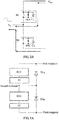
- FIG 1 is a schematic block diagram of a conventional totem pole circuit.
- the conventional totem pole circuit includes two series switching transistors S1 and S2.
- the switching transistor S1 includes a parasitic diode BD1 and a parasitic capacitor C1 internally
- the switching transistor S2 includes a parasitic diode BD2 and a parasitic capacitor C2 internally.
- V in may be an input end
- V out may be an output end.
- the conventional totem pole circuit may be applied to a scenario of synchronous rectification.
- FIG. 2A within a positive half cycle of an input alternating voltage, the switching transistor S1 is turned on, and the switching transistor S2 is turned off. A current flows through an intermediate node of the switching transistor S1 and the switching transistor S2, and flows out from the switching transistor S1.
- FIG. 2B within a negative half cycle of the alternating input voltage, the switching transistor S1 is turned off, and the switching transistor S2 is turned on. A current flows through the switching transistor S2, and flows out from the intermediate node of the switching transistor S1 and the switching transistor S2.
- the switching transistor S1 and the switching transistor S2 are turned on alternately, and the circuit may implement the synchronous rectification effect.
- the current is shown as a solid line in FIG. 2A , and the current flows through the switching transistor S1 that is turned on.
- the switching transistor S1 is turned off, and the parasitic diode BD1 of the switching transistor S1 generates a reverse recovery current that is shown as a dashed line in FIG 2B , adversely affecting the switching transistor S2 that is just turned on.
- a first diode, a second diode, a first bidirectional conduction network, and a second bidirectional conduction network are added to the conventional totem pole circuit, and the first switching transistor and the second switching transistor are controlled to be turned on or off at different times, to increase efficiency of the bidirectional conversion circuit, and avoid generation of a reverse recovery current in the circuit, thereby improving performance of the bidirectional conversion circuit.
- FIG. 3A is a schematic diagram of a circuit structure of a bidirectional conversion circuit 100 according to an embodiment of the present invention.
- the bidirectional conversion circuit 100 includes a first bidirectional conduction network D1d, a second bidirectional conduction network D2d, a first switching transistor S1, a second switching transistor S2, a first diode D1a, and a second diode D2a.
- the first bidirectional conduction network D1d and the first switching transistor S1 are connected in series to form a first branch, where a first end of the first branch is connected to a cathode of the first diode D1a to form a first endpoint.
- the second bidirectional conduction network D2d and the second switching transistor S2 are connected in series to form a second branch, where a second end of the second branch is connected to an anode of the second diode D2a to form a third endpoint.
- a second end of the first branch, an anode of the first diode D1a, a first end of the second branch, and a cathode of the second diode D2a are connected to form a second endpoint.
- the first switching transistor S1 is turned on from a first time t1 to a second time t2, and is turned off from the second time t2 to a fifth time t5.
- the second switching transistor S2 is turned off from the first time t1 to a third time t3, is turned on from the third time t3 to a fourth time t4, and is turned off from the fourth time t4 to the fifth time t5.
- the first branch and the first diode D1a are alternately turned on.
- a negative half cycle of the input alternating voltage which may be from the third time t3 to the fifth time t5
- the second branch and the second diode D2a are alternately turned on.
- the first diode D1a, the second diode D2a, the first bidirectional conduction network D1d, and the second bidirectional conduction network D2d are added based on the conventional totem pole circuit.
- the first switching transistor S1 or the second switching transistor S2 is controlled to be turned on or off from the first time t1 to the fifth time t5, to alternately turn on the first branch, the first diode D1a, the second branch, and the second diode D2a, so that a reverse recovery current cannot be generated in the circuit, and the circuit can implement bidirectional conversion of the alternating voltage/direct current voltage.
- the bidirectional conversion circuit when the first endpoint and the third endpoint are input ends, and the second endpoint is an output end, the bidirectional conversion circuit is an inverter circuit. Conversely, when the second endpoint is an input end, and the first endpoint and the third endpoint are output ends, the bidirectional conversion circuit is a rectification circuit.
- the first time t1 may be a start time of a positive half cycle of a current flowing into or flowing out of the second endpoint
- the third time t3 may be an end time of the positive half cycle of the current
- the second time t2 may be any time within a time interval from the first t0 time to the third time t3
- the fifth time t5 may be an end time of a negative half cycle of the current
- the fourth time t4 may be any time within a time interval from the third time t3 to the fifth time t5.
- the bidirectional conversion circuit 100 in this embodiment of the present invention may include a controller.
- the controller may be configured to control the first switching transistor S1 and the second switching transistor S2 to be turned on or off.
- the controller may control the first switching transistor S1 to be turned on from the first time t1 to the second time t2, and to be turned off from the second time t2 to the fifth time t5; and may control the second switching transistor S2 to be turned off from the first time t1 to the third time t3, to be turned on from the third time t3 to the fourth time t4, and to be turned off from the fourth time t4 to the fifth time t5.
- FIG. 3B is a schematic diagram of another circuit structure of a bidirectional conversion circuit according to an embodiment of the present invention.
- a switching transistor may include a parasitic capacitor and a parasitic diode.
- a first switching transistor S1 may include a parasitic capacitor C1 and a parasitic diode BD1
- a second switching transistor S2 may include a parasitic capacitor C2 and a parasitic diode BD2.
- the parasitic capacitor C1 and the parasitic capacitor C2 may be dischargeable in an inversion scenario, thereby implementing soft switching of the switching transistors.
- positions of the first switching transistor S1 and a first bidirectional conduction network D1d on a first branch are not limited in the bidirectional conversion circuit provided in this embodiment of the present invention.
- the first switching transistor S1 may approach a second endpoint, or the first bidirectional conduction network D1d may approach the second endpoint.
- positions of the second switching transistor S2 and a second bidirectional conduction network D2d on a second branch are not limited either.
- the second switching transistor S2 may approach the second endpoint, or the second bidirectional conduction network D2d may approach the second endpoint.
- a first diode D1a, a second diode D2a, the first bidirectional conduction network D1d, and the second bidirectional conduction network D2d are added to the conventional totem pole circuit, and the first switching transistor S1 and the second switching transistor S2 are controlled to be turned on or off at different times, to increase efficiency of the bidirectional conversion circuit, and avoid generation of a reverse recovery current in the circuit, thereby improving performance of the bidirectional conversion circuit.
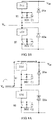
- FIG. 4A to FIG. 4D are schematic diagrams showing that the circuit structure shown in FIG. 3B is applied to a scenario of synchronous rectification.
- the first branch and the first diode D1a, and the second branch and the second diode D2a are alternately turned on for a current, so that an input alternating voltage is converted into a direct current voltage for output.
- a specific working process is shown in FIG 4A to FIG. 4D .
- V in may be an input end
- V out may be an output end.
- the second switching transistor S2 is turned off.
- the first switching transistor S1 is turned on, and a current may flow into the second endpoint, flow through the first branch, and flow out from a first endpoint.
- the first switching transistor S1 is turned off, and the current may flow into the second endpoint, flow through the first diode D1a, and flow out from the first endpoint.
- the first switching transistor S1 is turned off.
- the second switching transistor S2 is turned on, and the current may flow into a third endpoint, flow through the second branch, and flow out from the second endpoint.
- the second switching transistor S2 is turned off, and the current may flow into the third endpoint, flow through the second diode D2a, and flow out from the second endpoint.
- the current may choose to flow through a branch having a lower conduction voltage drop.
- the first switching transistor S1 is turned on, and the second switching transistor S2 is turned off.
- a conduction voltage drop of the first bidirectional conduction network D1d on the first branch is less than a conduction voltage drop of the first diode D1a.
- the current may flow into the second endpoint, flow through the first branch, and flow out from the first endpoint.
- the first switching transistor S1 is turned off, and the second switching transistor S2 is turned on.
- a conduction voltage drop of the second bidirectional conduction network D2d is less than a conduction voltage drop of the second diode D2a. The current may flow into the third endpoint, flow through the second branch, and flow out from the second endpoint.
- the current may be enabled to flow through the first diode D1a instead of the first switching transistor S1. Therefore, a sum of a conduction voltage drop of the first bidirectional conduction network D1d and a conduction voltage drop of the parasitic diode BD1 of the first switching transistor S1 may be greater than the conduction voltage drop of the first diode D1a.
- the current may be enabled to flow through the second diode D2a instead of the second switching transistor S2. Therefore, a sum of a conduction voltage drop of the second bidirectional conduction network D2d and a conduction voltage drop of the parasitic diode BD2 of the second switching transistor S2 may be greater than the conduction voltage drop of the second diode Da2.
- the conduction voltage drop of the first bidirectional conduction network D1d is 1 V
- the conduction voltage drop of the parasitic diode BD1 of the first switching transistor S1 is 1 V
- the conduction voltage drop of the first diode D1a is 1.5 V
- the sum of the conduction voltage drop of the first bidirectional conduction network D1d and the conduction voltage drop of the parasitic diode BD1 of the first switching transistor S1 is 2 V, and is greater than the conduction voltage drop of the first diode D1a.
- the current chooses to flow through the first diode D1a instead of the parasitic diode BD1 of the first switching transistor S1, to avoid generation of a reverse recovery current when the first switching transistor S1 is turned off at the third time t3.
- the current is enabled to flow through the first diode D1a instead of the first branch from the second time t2 to the third time t3, and to flow through the second diode D2a instead of the second branch from the fourth time t4 to the fifth time t5, to avoid generation of a reverse recovery current in a switching transistor in a scenario of synchronous rectification, thereby improving performance of the circuit.
- the current may be controlled to flow through the first branch and the second branch in most time, and to flow through the first diode D1a and the second diode D2a in little time.
- the second time t2 and the fourth time t4 may be times when the input alternating voltage approaches 0.
- a time interval from the first time t1 to the second time t2 is far greater than a time interval from the second time t2 to the third time t3
- a time interval from the third time t3 to the fourth time t4 is far greater than a time interval from the fourth time t4 to the fifth time t5.
- the conduction voltage drop of the first branch is less than the conduction voltage drop of the first diode D1a.
- the conduction voltage drop of the second branch is less than the conduction voltage drop of the second diode D2a. Therefore, the current in the circuit flows through the first branch and the second branch in most time, to avoid generation of a reverse recovery current while improving the rectification efficiency of the circuit.
- the first diode D1a and the second diode D2a may be fast recovery diodes or silicon carbide SiC diodes.
- the first bidirectional conduction network D1d or the second bidirectional conduction network D2d may be two parallel diodes D1 and D2 having opposite polarities.
- the first bidirectional conduction network D1d or the second bidirectional conduction network D2d may be one metal-oxide-semiconductor field-effect transistor, or may be at least two series metal-oxide-semiconductor field-effect transistors.
- the first bidirectional conduction network D1d or the second bidirectional conduction network D2d may alternatively be one insulated gate bipolar transistor, or may be at least two series insulated gate bipolar transistors.
- the first bidirectional conduction network D1d or the second bidirectional conduction network D2d may be one metal-oxide-semiconductor field-effect transistor Dc1 or one insulated gate bipolar transistor Dc1.
- the first bidirectional conduction network D1d or the second bidirectional conduction network D2d may be two series metal-oxide-semiconductor field-effect transistors Dc2 or two series insulated gate bipolar transistors Dc2.
- FIG. 7A to FIG. 7D are schematic diagrams showing that the circuit structure shown in FIG. 3B is applied to an inversion scenario.
- the first branch and the first diode D1a, and the second branch and the second diode D2a are alternately turned on for a current, so that an input direct current voltage is converted into an alternating voltage.
- a specific working process is shown in FIG. 7A to FIG. 7D .
- V in may be an input end
- V out may be an output end.
- the second switching transistor S2 is turned off.
- FIG. 7A from a first time t1 to a second time t2, the first switching transistor S1 is turned on, and a current may flow into a first endpoint, flow through the first branch, and flow out from the second endpoint.
- FIG. 7B from the second time t2 to a third time t3, the first switching transistor S1 is turned off, and the current may flow into a third endpoint, flow through the second branch, and flow out from the second endpoint.
- the first switching transistor S1 is turned off.
- the second switching transistor S2 is turned on, and the current may flow into the second endpoint, flow through the second branch, and flow out from the third endpoint.
- the second switching transistor S2 is turned off, and the current may flow into the second endpoint, flow through the first branch, and flow out from the first endpoint.
- the parasitic capacitor C2 may discharge by using the second bidirectional conduction network D2d.
- the parasitic capacitor C1 may discharge by using the first bidirectional conduction network D1d, so that the first switching transistor S1 and the second switching transistor S2 can implement soft switching, and the entire performance of the circuit can be improved.
- the first switching transistor S1 or the second switching transistor S2 may be an MOSFET or an IGBT.
- the bidirectional conversion circuit 100 in this embodiment of the present invention may also be applied to another scenario, for example, a scenario of bridgeless power factor correction.
- a bidirectional converter according to an embodiment of the present invention is described in detail below with reference to FIG. 8 and FIG. 9 .
- FIG. 8 is a schematic diagram of a circuit structure of a bidirectional converter 200 according to an embodiment of the present invention. As shown in FIG. 8 , the bidirectional converter 200 includes:
- one side of the bidirectional converter 200 may be connected to an alternating current power supply, and the other side of the bidirectional converter 200 may be connected to a direct current power supply.
- the alternating current power supply outputs an alternating voltage.
- the alternating voltage may be converted into a direct current voltage by using the bidirectional converter 200, and the direct current voltage is input into the direct current power supply.
- the direct current power supply outputs a direct current voltage.
- the direct current voltage may be converted into an alternating voltage by using the bidirectional converter 200, and the alternating voltage is input into the alternating current power supply, to implement bidirectional conversion of the alternating voltage/direct current voltage.
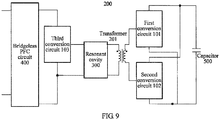
- FIG. 9 is a schematic diagram of another circuit structure of a bidirectional converter according to an embodiment of the present invention.
- the bidirectional converter 200 may further include a capacitor 500, where a first endpoint of the first bidirectional conversion circuit 101 is connected to a first endpoint of the second bidirectional conversion circuit 102 and is connected to a positive end of the capacitor 500, and a third endpoint of the first bidirectional conversion circuit 101 is connected to a third endpoint of the second bidirectional conversion circuit 102 and is connected to a negative end of the capacitor 500.
- the disclosed system, apparatus, and method may be implemented in other manners.
- the described apparatus embodiment is merely an example.
- the unit division is merely logical function division and may be other division in actual implementation.
- a plurality of units or components may be combined or integrated into another system, or some features may be ignored or not performed.
- the displayed or discussed mutual couplings or direct couplings or communication connections may be implemented by using some interfaces.
- the indirect couplings or communication connections between the apparatuses or units may be implemented in electronic, mechanical, or other forms.
- the units described as separate parts may or may not be physically separate, and parts displayed as units may or may not be physical units, may be located in one position, or may be distributed on a plurality of network units. Some or all of the units may be selected according to actual requirements to achieve the objectives of the solutions of the embodiments.
- functional units in the embodiments of the present invention may be integrated into one processing unit, or each of the units may exist alone physically, or two or more units are integrated into one unit.
- the functions When the functions are implemented in the form of a software functional unit and sold or used as an independent product, the functions may be stored in a computer-readable storage medium.
- the software product is stored in a storage medium, and includes several instructions for instructing a computer device (which may be a personal computer, a server, or a network device) to perform all or some of the steps of the methods described in the embodiments of the present invention.
- the foregoing storage medium includes: any medium that can store program code, such as a USB flash drive, a removable hard disk, a read-only memory (ROM), a random access memory (RAM), a magnetic disk, or an optical disc.
Landscapes
- Engineering & Computer Science (AREA)
- Power Engineering (AREA)
- Rectifiers (AREA)
- Dc-Dc Converters (AREA)
- Inverter Devices (AREA)
Abstract
Description
- This application claims priority to Chinese Patent Application No.
201510976555.4 - This application relates to the power conversion field, and in particular, to a bidirectional conversion circuit and a bidirectional converter in power conversion technologies.
- A conventional totem pole circuit includes two series switching transistors, and the switching transistors each have a parasitic diode and a parasitic capacitor internally.
- If a conventional totem pole operates in a scenario of synchronous rectification, a current is continuous, and an output voltage is a high voltage greater than 400 V, a device having a withstand voltage of more than 400 V is selected as the switching transistor. A reverse recovery current of a parasitic diode of such device is relatively large.
- When a switching transistor is turned off, a reverse recovery current generated by a parasitic diode of the switching transistor may adversely affect the other parasitic switching transistor that is just turned on, and may further affect an operating state of an entire circuit in a severe case.
- Embodiments of the present invention provide a bidirectional conversion circuit and a bidirectional converter, to resolve a problem that a conventional totem pole circuit generates a reverse recovery current in a scenario of synchronous rectification.
- According to a first aspect, an embodiment of the present invention provides a bidirectional conversion circuit, where the bidirectional conversion circuit includes:
- a first bidirectional conduction network, a second bidirectional conduction network, a first switching transistor, a second switching transistor, a first diode, and a second diode, where
- the first bidirectional conduction network and the first switching transistor are connected in series to form a first branch, where a first end of the first branch is connected to a cathode of the first diode to form a first endpoint;
- the second bidirectional conduction network and the second switching transistor are connected in series to form a second branch, where a second end of the second branch is connected to an anode of the second diode to form a third endpoint;
- a second end of the first branch, an anode of the first diode, a first end of the second branch, and a cathode of the second diode are connected to form a second endpoint;
- the first switching transistor is turned on from a first time to a second time, and is turned off from the second time to a fifth time; and
- the second switching transistor is turned off from the first time to a third time, is turned on from the third time to a fourth time, and is turned off from the fourth time to the fifth time, where
- the first time is a start time of a positive half cycle of a current flowing into or flowing out of the second endpoint, the third time is an end time of the positive half cycle of the current, the second time is any time within a time interval from the first time to the third time, the fifth time is an end time of a negative half cycle of the current, and the fourth time is any time within a time interval from the third time to the fifth time.
- Therefore, the first diode, the second diode, the first bidirectional conduction network, and the second bidirectional conduction network are added to the conventional totem pole circuit, and the first switching transistor and the second switching transistor are controlled to be turned on or off at different times, to avoid generation of a reverse recovery current in the circuit, thereby improving performance of the bidirectional conversion circuit.
- With reference to the first aspect, it may be understood that, the first bidirectional conduction network is a metal-oxide-semiconductor field-effect transistor (MOSFET for short), an insulated gate bipolar transistor (IGBT for short), or two parallel diodes having opposite polarities. The MOSFET may be one MOSFET or at least two series MOSFETs, and the IGBT may be one IGBT or at least two series IGBTs.
- With reference to the first aspect, it may be understood that, the second bidirectional conduction network is an MOSFET, an IGBT, or two parallel diodes having opposite polarities. The MOSFET may be one MOSFET or at least two series MOSFETs, and the IGBT may be one IGBT or at least two series IGBTs.
- With reference to the first aspect, it may be understood that, a conduction voltage drop of the first bidirectional conduction network is less than a conduction voltage drop of the first diode, and a sum of the conduction voltage drop of the first bidirectional conduction network and a conduction voltage drop of a parasitic diode of the first switching transistor is greater than the conduction voltage drop of the first diode; and a conduction voltage drop of the second bidirectional conduction network is less than a conduction voltage drop of the second diode, and a sum of the conduction voltage drop of the second bidirectional conduction network and a conduction voltage drop of a parasitic diode of the second switching transistor is greater than the conduction voltage drop of the second diode.
- With reference to the first aspect, optionally, the first switching transistor is a metal-oxide-semiconductor field-effect transistor MOSFET or an insulated gate bipolar transistor IGBT; and the second switching transistor is an MOSFET or an IGBT.
- With reference to the first aspect, optionally, the first diode is a fast recovery diode or a silicon carbide SiC diode; and the second diode is a fast recovery diode or a silicon carbide SiC diode.
- With reference to the first aspect, it may be understood that, the bidirectional conversion circuit is used for a synchronous rectification circuit or an inverter circuit.
- With reference to the first aspect, it may be understood that, the bidirectional conversion circuit further includes a controller, where the controller is configured to: control the first switching transistor to be turned on or off;
control the second switching transistor to be turned on or off; or
control the first switching transistor and the second switching transistor to be turned on or off. - Therefore, the bidirectional conversion circuit provided in this embodiment of the present invention may be applied to a scenario of synchronous rectification, to resolve a problem of a reverse recovery current of high voltage synchronous rectification, and can increase the rectification efficiency at the same time. The bidirectional conversion circuit may also be used in an inversion scenario. In the inversion scenario, parasitic capacitors of the switching transistors are dischargeable.
- According to a second aspect, a bidirectional converter is provided, where the bidirectional converter includes:
- a first bidirectional conversion circuit according to the first aspect or any implementation of the first aspect; a second bidirectional conversion circuit according to the first aspect or any implementation of the first aspect; and a third bidirectional conversion circuit according to the first aspect or any implementation of the first aspect;
- a transformer, where the transformer includes a primary-side winding and a secondary-side winding, one end of the secondary-side winding of the transformer is connected to a second endpoint of the first bidirectional conversion circuit, and the other end of the secondary-side winding of the transformer is connected to a second endpoint of the second bidirectional conversion circuit;
- a resonant cavity, where the resonant cavity includes a first port, a second port, a third port, and a fourth port, the first port is connected to a second endpoint of the third bidirectional conversion circuit, the second port is connected to a third endpoint of the third bidirectional conversion circuit, and the third port and the fourth port are separately connected to the primary-side winding of the transformer; and
- a bridgeless PFC circuit, where the bridgeless PFC circuit includes two alternating current ports and two direct current ports, and the two direct current ports are separately connected to a first endpoint and the third endpoint of the third bidirectional conversion circuit.
- With reference to the second aspect, it may be understood that, the bidirectional converter further includes: a capacitor, where a first endpoint of the first bidirectional conversion circuit is connected to a first endpoint of the second bidirectional conversion circuit and is connected to a positive end of the capacitor, and a third endpoint of the first bidirectional conversion circuit is connected to a third endpoint of the second bidirectional conversion circuit and is connected to a negative end of the capacitor.
- Based on the foregoing technical solutions, the first diode, the second diode, the first bidirectional conduction network, and the second bidirectional conduction network are added to the conventional totem pole circuit, and the first switching transistor and the second switching transistor are controlled to be turned on or off at different times, to increase efficiency of the bidirectional conversion circuit, and avoid generation of a reverse recovery current in the circuit, thereby improving performance of the bidirectional conversion circuit.
-
-
FIG. 1 is a schematic diagram of a conventional totem pole circuit structure; -
FIG. 2A andFIG 2B are schematic diagrams showing that the circuit structure shown inFIG. 1 is applied to a scenario of synchronous rectification; -
FIG 3A is a schematic diagram of a circuit structure of a bidirectional conversion circuit according to an embodiment of the present invention; -
FIG. 3B is a schematic diagram of another circuit structure of a bidirectional conversion circuit according to an embodiment of the present invention; -
FIG. 4A to FIG. 4D are schematic diagrams showing that the circuit structure shown inFIG. 3B is applied to a scenario of synchronous rectification; -
FIG. 5 is a schematic diagram of a circuit structure of a bidirectional conduction network according to an embodiment of the present invention; -
FIG 6A andFIG. 6B are schematic diagrams of another circuit structure of a bidirectional conduction network according to an embodiment of the present invention; -
FIG 7A to FIG. 7D are schematic diagrams showing that the circuit structure shown inFIG. 3B is applied to an inversion scenario; -
FIG. 8 is a schematic diagram of a circuit structure of a bidirectional converter according to an embodiment of the present invention; and -
FIG. 9 is a schematic diagram of another circuit structure of a bidirectional converter according to an embodiment of the present invention. - The following describes the technical solutions in the embodiments of the present invention with reference to the accompanying drawings in the embodiments of the present invention.
-
FIG 1 is a schematic block diagram of a conventional totem pole circuit. As shown inFIG 1 , the conventional totem pole circuit includes two series switching transistors S1 and S2. The switching transistor S1 includes a parasitic diode BD1 and a parasitic capacitor C1 internally, and the switching transistor S2 includes a parasitic diode BD2 and a parasitic capacitor C2 internally. Vin may be an input end, and Vout may be an output end. - The conventional totem pole circuit may be applied to a scenario of synchronous rectification. As shown in
FIG. 2A , within a positive half cycle of an input alternating voltage, the switching transistor S1 is turned on, and the switching transistor S2 is turned off. A current flows through an intermediate node of the switching transistor S1 and the switching transistor S2, and flows out from the switching transistor S1. As shown inFIG. 2B , within a negative half cycle of the alternating input voltage, the switching transistor S1 is turned off, and the switching transistor S2 is turned on. A current flows through the switching transistor S2, and flows out from the intermediate node of the switching transistor S1 and the switching transistor S2. The switching transistor S1 and the switching transistor S2 are turned on alternately, and the circuit may implement the synchronous rectification effect. - It should be understood that, because reverse recovery currents of the parasitic diodes of the two switching transistors are relatively large, a reverse recovery current resulted from turning off a switching transistor may adversely affect the other switching transistor that is just turned on, and may affect an operating state of the entire circuit in a severe case.
- For example, as shown in
FIG. 2A andFIG. 2B , within the positive half cycle of the alternating input voltage, the current is shown as a solid line inFIG. 2A , and the current flows through the switching transistor S1 that is turned on. Within the negative half cycle of the alternating input voltage, the switching transistor S1 is turned off, and the parasitic diode BD1 of the switching transistor S1 generates a reverse recovery current that is shown as a dashed line inFIG 2B , adversely affecting the switching transistor S2 that is just turned on. - Therefore, according to a bidirectional conversion circuit and a bidirectional converter in the embodiments of the present invention, a first diode, a second diode, a first bidirectional conduction network, and a second bidirectional conduction network are added to the conventional totem pole circuit, and the first switching transistor and the second switching transistor are controlled to be turned on or off at different times, to increase efficiency of the bidirectional conversion circuit, and avoid generation of a reverse recovery current in the circuit, thereby improving performance of the bidirectional conversion circuit.
-
FIG. 3A is a schematic diagram of a circuit structure of a bidirectional conversion circuit 100 according to an embodiment of the present invention. The bidirectional conversion circuit 100 includes a first bidirectional conduction network D1d, a second bidirectional conduction network D2d, a first switching transistor S1, a second switching transistor S2, a first diode D1a, and a second diode D2a. - The first bidirectional conduction network D1d and the first switching transistor S1 are connected in series to form a first branch, where a first end of the first branch is connected to a cathode of the first diode D1a to form a first endpoint.
- The second bidirectional conduction network D2d and the second switching transistor S2 are connected in series to form a second branch, where a second end of the second branch is connected to an anode of the second diode D2a to form a third endpoint.
- A second end of the first branch, an anode of the first diode D1a, a first end of the second branch, and a cathode of the second diode D2a are connected to form a second endpoint.
- The first switching transistor S1 is turned on from a first time t1 to a second time t2, and is turned off from the second time t2 to a fifth time t5. The second switching transistor S2 is turned off from the first time t1 to a third time t3, is turned on from the third time t3 to a fourth time t4, and is turned off from the fourth time t4 to the fifth time t5.
- Optionally, within a positive half cycle of an input alternating voltage, which may be from the first time t1 to the third time t3, the first branch and the first diode D1a are alternately turned on. Within a negative half cycle of the input alternating voltage, which may be from the third time t3 to the fifth time t5, the second branch and the second diode D2a are alternately turned on.
- Specifically, according to the bidirectional conversion circuit in this embodiment of the present invention, the first diode D1a, the second diode D2a, the first bidirectional conduction network D1d, and the second bidirectional conduction network D2d are added based on the conventional totem pole circuit. In addition, the first switching transistor S1 or the second switching transistor S2 is controlled to be turned on or off from the first time t1 to the fifth time t5, to alternately turn on the first branch, the first diode D1a, the second branch, and the second diode D2a, so that a reverse recovery current cannot be generated in the circuit, and the circuit can implement bidirectional conversion of the alternating voltage/direct current voltage.
- For example, when the first endpoint and the third endpoint are input ends, and the second endpoint is an output end, the bidirectional conversion circuit is an inverter circuit. Conversely, when the second endpoint is an input end, and the first endpoint and the third endpoint are output ends, the bidirectional conversion circuit is a rectification circuit.
- Optionally, the first time t1 may be a start time of a positive half cycle of a current flowing into or flowing out of the second endpoint, the third time t3 may be an end time of the positive half cycle of the current, the second time t2 may be any time within a time interval from the first t0 time to the third time t3, the fifth time t5 may be an end time of a negative half cycle of the current, and the fourth time t4 may be any time within a time interval from the third time t3 to the fifth time t5.
- Optionally, the bidirectional conversion circuit 100 in this embodiment of the present invention may include a controller. The controller may be configured to control the first switching transistor S1 and the second switching transistor S2 to be turned on or off.
- Specifically, the controller may control the first switching transistor S1 to be turned on from the first time t1 to the second time t2, and to be turned off from the second time t2 to the fifth time t5; and may control the second switching transistor S2 to be turned off from the first time t1 to the third time t3, to be turned on from the third time t3 to the fourth time t4, and to be turned off from the fourth time t4 to the fifth time t5.
-
FIG. 3B is a schematic diagram of another circuit structure of a bidirectional conversion circuit according to an embodiment of the present invention. A switching transistor may include a parasitic capacitor and a parasitic diode. Specifically, a first switching transistor S1 may include a parasitic capacitor C1 and a parasitic diode BD1, and a second switching transistor S2 may include a parasitic capacitor C2 and a parasitic diode BD2. - It should be understood that, the parasitic capacitor C1 and the parasitic capacitor C2 may be dischargeable in an inversion scenario, thereby implementing soft switching of the switching transistors.
- It should be further understood that, positions of the first switching transistor S1 and a first bidirectional conduction network D1d on a first branch are not limited in the bidirectional conversion circuit provided in this embodiment of the present invention. For example, the first switching transistor S1 may approach a second endpoint, or the first bidirectional conduction network D1d may approach the second endpoint. Similarly, positions of the second switching transistor S2 and a second bidirectional conduction network D2d on a second branch are not limited either. For example, the second switching transistor S2 may approach the second endpoint, or the second bidirectional conduction network D2d may approach the second endpoint.
- Based on the foregoing technical solutions, according to the bidirectional conversion circuit and a bidirectional converter in the embodiments of the present invention, a first diode D1a, a second diode D2a, the first bidirectional conduction network D1d, and the second bidirectional conduction network D2d are added to the conventional totem pole circuit, and the first switching transistor S1 and the second switching transistor S2 are controlled to be turned on or off at different times, to increase efficiency of the bidirectional conversion circuit, and avoid generation of a reverse recovery current in the circuit, thereby improving performance of the bidirectional conversion circuit.
-
FIG. 4A to FIG. 4D are schematic diagrams showing that the circuit structure shown inFIG. 3B is applied to a scenario of synchronous rectification. As shown inFIG. 4A to FIG 4D , the first branch and the first diode D1a, and the second branch and the second diode D2a are alternately turned on for a current, so that an input alternating voltage is converted into a direct current voltage for output. A specific working process is shown inFIG 4A to FIG. 4D . - Vin may be an input end, and Vout may be an output end. Within a positive half cycle of an input alternating voltage, the second switching transistor S2 is turned off. As shown in
FIG. 4A , from a first time t1 to a second time t2, the first switching transistor S1 is turned on, and a current may flow into the second endpoint, flow through the first branch, and flow out from a first endpoint. As shown inFIG 4B , from the second time t2 to a third time t3, the first switching transistor S1 is turned off, and the current may flow into the second endpoint, flow through the first diode D1a, and flow out from the first endpoint. - Within a negative half cycle of the input alternating voltage, the first switching transistor S1 is turned off. As shown in
FIG. 4C , from the third time t3 to a fourth time t4, the second switching transistor S2 is turned on, and the current may flow into a third endpoint, flow through the second branch, and flow out from the second endpoint. As shown inFIG. 4D , from the fourth time t4 to a fifth time t5, the second switching transistor S2 is turned off, and the current may flow into the third endpoint, flow through the second diode D2a, and flow out from the second endpoint. - Specifically, the current may choose to flow through a branch having a lower conduction voltage drop. From the first time t1 to the second time t2 in the positive half cycle of the input alternating voltage, the first switching transistor S1 is turned on, and the second switching transistor S2 is turned off. A conduction voltage drop of the first bidirectional conduction network D1d on the first branch is less than a conduction voltage drop of the first diode D1a. The current may flow into the second endpoint, flow through the first branch, and flow out from the first endpoint. Similarly, from the third time t3 to the fourth time t4 of the negative half cycle of the input alternating voltage, the first switching transistor S1 is turned off, and the second switching transistor S2 is turned on. A conduction voltage drop of the second bidirectional conduction network D2d is less than a conduction voltage drop of the second diode D2a. The current may flow into the third endpoint, flow through the second branch, and flow out from the second endpoint.
- It should be understood that, from the third time t3 to the fourth time t4 of the positive half cycle of the input alternating voltage, to avoid that a reverse recovery current is generated instantly after the first switching transistor S1 is turned off, the current may be enabled to flow through the first diode D1a instead of the first switching transistor S1. Therefore, a sum of a conduction voltage drop of the first bidirectional conduction network D1d and a conduction voltage drop of the parasitic diode BD1 of the first switching transistor S1 may be greater than the conduction voltage drop of the first diode D1a. From the fourth time t4 to the fifth time t5 of the negative half cycle of the input alternating voltage, to avoid that a reverse recovery current is generated instantly after the second switching transistor S2 is turned off, the current may be enabled to flow through the second diode D2a instead of the second switching transistor S2. Therefore, a sum of a conduction voltage drop of the second bidirectional conduction network D2d and a conduction voltage drop of the parasitic diode BD2 of the second switching transistor S2 may be greater than the conduction voltage drop of the second diode Da2.
- For example, the conduction voltage drop of the first bidirectional conduction network D1d is 1 V, the conduction voltage drop of the parasitic diode BD1 of the first switching transistor S1 is 1 V, and the conduction voltage drop of the first diode D1a is 1.5 V. The sum of the conduction voltage drop of the first bidirectional conduction network D1d and the conduction voltage drop of the parasitic diode BD1 of the first switching transistor S1 is 2 V, and is greater than the conduction voltage drop of the first diode D1a. Therefore, from the second time t2 to the third time t3, the current chooses to flow through the first diode D1a instead of the parasitic diode BD1 of the first switching transistor S1, to avoid generation of a reverse recovery current when the first switching transistor S1 is turned off at the third time t3.
- It should be understood that, when this embodiment of the present invention is used in a synchronous rectification circuit, the current is enabled to flow through the first diode D1a instead of the first branch from the second time t2 to the third time t3, and to flow through the second diode D2a instead of the second branch from the fourth time t4 to the fifth time t5, to avoid generation of a reverse recovery current in a switching transistor in a scenario of synchronous rectification, thereby improving performance of the circuit.
- It should be further understood that, in the circuit, to increase the rectification efficiency, the current may be controlled to flow through the first branch and the second branch in most time, and to flow through the first diode D1a and the second diode D2a in little time. For example, the second time t2 and the fourth time t4 may be times when the input alternating voltage approaches 0. In this case, a time interval from the first time t1 to the second time t2 is far greater than a time interval from the second time t2 to the third time t3, and a time interval from the third time t3 to the fourth time t4 is far greater than a time interval from the fourth time t4 to the fifth time t5. In addition, when the first switching transistor S1 is turned on, the conduction voltage drop of the first branch is less than the conduction voltage drop of the first diode D1a. When the second switching transistor S2 is turned on, the conduction voltage drop of the second branch is less than the conduction voltage drop of the second diode D2a. Therefore, the current in the circuit flows through the first branch and the second branch in most time, to avoid generation of a reverse recovery current while improving the rectification efficiency of the circuit.
- Optionally, in this embodiment of the present invention, the first diode D1a and the second diode D2a may be fast recovery diodes or silicon carbide SiC diodes.
- Optionally, as shown in
FIG. 5 , the first bidirectional conduction network D1d or the second bidirectional conduction network D2d may be two parallel diodes D1 and D2 having opposite polarities. - Optionally, the first bidirectional conduction network D1d or the second bidirectional conduction network D2d may be one metal-oxide-semiconductor field-effect transistor, or may be at least two series metal-oxide-semiconductor field-effect transistors.
- Optionally, the first bidirectional conduction network D1d or the second bidirectional conduction network D2d may alternatively be one insulated gate bipolar transistor, or may be at least two series insulated gate bipolar transistors.
- For example, as shown in
FIG. 6A , the first bidirectional conduction network D1d or the second bidirectional conduction network D2d may be one metal-oxide-semiconductor field-effect transistor Dc1 or one insulated gate bipolar transistor Dc1. Alternatively, as shown inFIG. 6B , the first bidirectional conduction network D1d or the second bidirectional conduction network D2d may be two series metal-oxide-semiconductor field-effect transistors Dc2 or two series insulated gate bipolar transistors Dc2. -
FIG. 7A to FIG. 7D are schematic diagrams showing that the circuit structure shown inFIG. 3B is applied to an inversion scenario. As shown inFIG. 7A to FIG. 7D , the first branch and the first diode D1a, and the second branch and the second diode D2a are alternately turned on for a current, so that an input direct current voltage is converted into an alternating voltage. A specific working process is shown inFIG. 7A to FIG. 7D . - Vin may be an input end, and Vout may be an output end. Within a positive half cycle of an output alternating voltage, the second switching transistor S2 is turned off. As shown in
FIG. 7A , from a first time t1 to a second time t2, the first switching transistor S1 is turned on, and a current may flow into a first endpoint, flow through the first branch, and flow out from the second endpoint. As shown inFIG. 7B , from the second time t2 to a third time t3, the first switching transistor S1 is turned off, and the current may flow into a third endpoint, flow through the second branch, and flow out from the second endpoint. - Within a negative half cycle of the output alternating voltage, the first switching transistor S1 is turned off. As shown in
FIG. 7C , from the third time t3 to a fourth time t4, the second switching transistor S2 is turned on, and the current may flow into the second endpoint, flow through the second branch, and flow out from the third endpoint. As shown inFIG 7D , from the fourth time t4 to a fifth time t5, the second switching transistor S2 is turned off, and the current may flow into the second endpoint, flow through the first branch, and flow out from the first endpoint. - Specifically, from the second time t2 to the third time t3, the first switching transistor S1 and the second switching transistor S2 are turned off, and the parasitic capacitor C2 may discharge by using the second bidirectional conduction network D2d. Similarly, from the fourth time t4 to the fifth time t5, the parasitic capacitor C1 may discharge by using the first bidirectional conduction network D1d, so that the first switching transistor S1 and the second switching transistor S2 can implement soft switching, and the entire performance of the circuit can be improved.
- Optionally, the first switching transistor S1 or the second switching transistor S2 may be an MOSFET or an IGBT.
- It should be understood that, the bidirectional conversion circuit 100 in this embodiment of the present invention may also be applied to another scenario, for example, a scenario of bridgeless power factor correction.
- A bidirectional converter according to an embodiment of the present invention is described in detail below with reference to
FIG. 8 andFIG. 9 . -
FIG. 8 is a schematic diagram of a circuit structure of abidirectional converter 200 according to an embodiment of the present invention. As shown inFIG. 8 , thebidirectional converter 200 includes: - a first
bidirectional conversion circuit 101 described above; a secondbidirectional conversion circuit 102 described above; and a thirdbidirectional conversion circuit 103 described above; - a
transformer 201, including a primary-side winding and a secondary-side winding, where one end of the secondary-side winding of the transformer is connected to a second endpoint of the firstbidirectional conversion circuit 101, and the other end of the secondary-side winding of the transformer is connected to a second endpoint of the secondbidirectional conversion circuit 102; - a
resonant cavity 300, including a first port, a second port, a third port, and a fourth port, where the first port is connected to a second endpoint of the thirdbidirectional conversion circuit 103, the second port is connected to a third endpoint of the thirdbidirectional conversion circuit 103, and the third port and the fourth port are separately connected to the primary-side winding of thetransformer 201; and - a
bridgeless PFC circuit 400, including two alternating current ports and two direct current ports, where the two direct current ports are separately connected to a first endpoint and the third endpoint of the thirdbidirectional conversion circuit 103. - Specifically, one side of the
bidirectional converter 200 may be connected to an alternating current power supply, and the other side of thebidirectional converter 200 may be connected to a direct current power supply. The alternating current power supply outputs an alternating voltage. The alternating voltage may be converted into a direct current voltage by using thebidirectional converter 200, and the direct current voltage is input into the direct current power supply. The direct current power supply outputs a direct current voltage. The direct current voltage may be converted into an alternating voltage by using thebidirectional converter 200, and the alternating voltage is input into the alternating current power supply, to implement bidirectional conversion of the alternating voltage/direct current voltage. - Optionally, as shown in
FIG. 9, FIG. 9 is a schematic diagram of another circuit structure of a bidirectional converter according to an embodiment of the present invention. Thebidirectional converter 200 may further include acapacitor 500, where a first endpoint of the firstbidirectional conversion circuit 101 is connected to a first endpoint of the secondbidirectional conversion circuit 102 and is connected to a positive end of thecapacitor 500, and a third endpoint of the firstbidirectional conversion circuit 101 is connected to a third endpoint of the secondbidirectional conversion circuit 102 and is connected to a negative end of thecapacitor 500. - A person of ordinary skill in the art may be aware that, in combination with the examples described in the embodiments disclosed in this specification, units and algorithm steps may be implemented by electronic hardware or a combination of computer software and electronic hardware. Whether the functions are performed by hardware or software depends on particular applications and design constraint conditions of the technical solutions. A person skilled in the art may use different methods to implement the described functions for each particular application, but it should not be considered that the implementation goes beyond the scope of this application.
- It may be clearly understood by a person skilled in the art that, for the purpose of convenient and brief description, for a detailed working process of the foregoing system, apparatus, and unit, refer to a corresponding process in the foregoing method embodiments, and details are not described herein again.
- In the several embodiments provided in this application, it should be understood that the disclosed system, apparatus, and method may be implemented in other manners. For example, the described apparatus embodiment is merely an example. For example, the unit division is merely logical function division and may be other division in actual implementation. For example, a plurality of units or components may be combined or integrated into another system, or some features may be ignored or not performed. In addition, the displayed or discussed mutual couplings or direct couplings or communication connections may be implemented by using some interfaces. The indirect couplings or communication connections between the apparatuses or units may be implemented in electronic, mechanical, or other forms.
- The units described as separate parts may or may not be physically separate, and parts displayed as units may or may not be physical units, may be located in one position, or may be distributed on a plurality of network units. Some or all of the units may be selected according to actual requirements to achieve the objectives of the solutions of the embodiments.
- In addition, functional units in the embodiments of the present invention may be integrated into one processing unit, or each of the units may exist alone physically, or two or more units are integrated into one unit.
- When the functions are implemented in the form of a software functional unit and sold or used as an independent product, the functions may be stored in a computer-readable storage medium. Based on such an understanding, the technical solutions of the embodiments of the present invention essentially, or the part contributing to the prior art, or some of the technical solutions may be implemented in a form of a software product. The software product is stored in a storage medium, and includes several instructions for instructing a computer device (which may be a personal computer, a server, or a network device) to perform all or some of the steps of the methods described in the embodiments of the present invention. The foregoing storage medium includes: any medium that can store program code, such as a USB flash drive, a removable hard disk, a read-only memory (ROM), a random access memory (RAM), a magnetic disk, or an optical disc.
- The foregoing descriptions are merely specific implementation manners of this application, but are not intended to limit the protection scope of this application. Any variation or replacement readily figured out by a person skilled in the art within the technical scope disclosed in this application shall fall within the protection scope of this application. Therefore, the protection scope of the present application shall be subject to the protection scope of the claims.
Claims (10)
- A bidirectional conversion circuit, comprising:a first bidirectional conduction network, a second bidirectional conduction network, a first switching transistor, a second switching transistor, a first diode, and a second diode, whereinthe first bidirectional conduction network and the first switching transistor are connected in series to form a first branch, wherein a first end of the first branch is connected to a cathode of the first diode to form a first endpoint;the second bidirectional conduction network and the second switching transistor are connected in series to form a second branch, wherein a second end of the second branch is connected to an anode of the second diode to form a third endpoint;a second end of the first branch, an anode of the first diode, a first end of the second branch, and a cathode of the second diode are connected to form a second endpoint;the first switching transistor is turned on from a first time to a second time, and is turned off from the second time to a fifth time; andthe second switching transistor is turned off from the first time to a third time, is turned on from the third time to a fourth time, and is turned off from the fourth time to the fifth time, whereinthe first time is a start time of a positive half cycle of a current flowing into or flowing out of the second endpoint, the third time is an end time of the positive half cycle of the current, the second time is any time within a time interval from the first time to the third time, the fifth time is an end time of a negative half cycle of the current, and the fourth time is any time within a time interval from the third time to the fifth time.
- The bidirectional conversion circuit according to claim 1, wherein the first bidirectional conduction network is a metal-oxide-semiconductor field-effect transistor MOSFET, an insulated gate bipolar transistor IGBT, or two parallel diodes having opposite polarities.
- The bidirectional conversion circuit according to claim 1 or 2, wherein the second bidirectional conduction network is an MOSFET, an IGBT, or two parallel diodes having opposite polarities.
- The bidirectional conversion circuit according to any one of claims 1 to 3, wherein
a conduction voltage drop of the first bidirectional conduction network is less than a conduction voltage drop of the first diode, and a sum of the conduction voltage drop of the first bidirectional conduction network and a conduction voltage drop of a parasitic diode of the first switching transistor is greater than the conduction voltage drop of the first diode; and
a conduction voltage drop of the second bidirectional conduction network is less than a conduction voltage drop of the second diode, and a sum of the conduction voltage drop of the second bidirectional conduction network and a conduction voltage drop of a parasitic diode of the second switching transistor is greater than the conduction voltage drop of the second diode. - The bidirectional conversion circuit according to any one of claims 1 to 4, wherein
the first switching transistor is a metal-oxide-semiconductor field-effect transistor MOSFET or an insulated gate bipolar transistor IGBT; and
the second switching transistor is an MOSFET or an IGBT. - The bidirectional conversion circuit according to any one of claims 1 to 5, wherein the first diode is a fast recovery diode or a silicon carbide SiC diode; and
the second diode is a fast recovery diode or a silicon carbide SiC diode. - The bidirectional conversion circuit according to any one of claims 1 to 6, wherein the bidirectional conversion circuit is used for a synchronous rectification circuit or an inverter circuit.
- The bidirectional conversion circuit according to any one of claims 1 to 7, wherein the bidirectional conversion circuit further comprises a controller, wherein
the controller is configured to: control the first switching transistor to be turned on or off; control the second switching transistor to be turned on or off; or
control the first switching transistor and the second switching transistor to be turned on or off. - A bidirectional converter, comprising:a first bidirectional conversion circuit according to any one of claims 1 to 8;a second bidirectional conversion circuit according to any one of claims 1 to 8;a third bidirectional conversion circuit according to any one of claims 1 to 8;a transformer, wherein the transformer comprises a primary-side winding and a secondary-side winding, one end of the secondary-side winding of the transformer is connected to a second endpoint of the first bidirectional conversion circuit, and the other end of the secondary-side winding of the transformer is connected to a second endpoint of the second bidirectional conversion circuit;a resonant cavity, wherein the resonant cavity comprises a first port, a second port, a third port, and a fourth port, the first port is connected to a second endpoint of the third bidirectional conversion circuit, the second port is connected to a third endpoint of the third bidirectional conversion circuit, and the third port and the fourth port are separately connected to the primary-side winding of the transformer; anda bridgeless PFC circuit, wherein the bridgeless PFC circuit comprises two alternating current ports and two direct current ports, and the two direct current ports are separately connected to a first endpoint and the third endpoint of the third bidirectional conversion circuit.
- The bidirectional converter according to claim 9, wherein the bidirectional converter further comprises:a capacitor, wherein a first endpoint of the first bidirectional conversion circuit is connected to a first endpoint of the second bidirectional conversion circuit and is connected to a positive end of the capacitor, and a third endpoint of the first bidirectional conversion circuit is connected to a third endpoint of the second bidirectional conversion circuit and is connected to a negative end of the capacitor.
Applications Claiming Priority (2)
| Application Number | Priority Date | Filing Date | Title |
|---|---|---|---|
| CN201510976555.4A CN106911262B (en) | 2015-12-22 | 2015-12-22 | Bidirectional conversion circuit and bidirectional converter |
| PCT/CN2016/108605 WO2017107765A1 (en) | 2015-12-22 | 2016-12-05 | Bidirectional conversion circuit and bidirectional converter |
Publications (2)
| Publication Number | Publication Date |
|---|---|
| EP3396842A1 true EP3396842A1 (en) | 2018-10-31 |
| EP3396842A4 EP3396842A4 (en) | 2019-01-09 |
Family
ID=59089068
Family Applications (1)
| Application Number | Title | Priority Date | Filing Date |
|---|---|---|---|
| EP16877576.5A Pending EP3396842A4 (en) | 2015-12-22 | 2016-12-05 | BIDIRECTIONAL CONVERSION CIRCUIT AND TWO-WAY CONVERTER |
Country Status (6)
| Country | Link |
|---|---|
| US (1) | US10666164B2 (en) |
| EP (1) | EP3396842A4 (en) |
| JP (1) | JP6571286B2 (en) |
| KR (1) | KR102130362B1 (en) |
| CN (1) | CN106911262B (en) |
| WO (1) | WO2017107765A1 (en) |
Families Citing this family (3)
| Publication number | Priority date | Publication date | Assignee | Title |
|---|---|---|---|---|
| TWI670702B (en) * | 2018-07-24 | 2019-09-01 | 友達光電股份有限公司 | Dual gate transistor circuit, pixel circuit and gate drive circuit therof |
| CN113039712B (en) * | 2019-06-26 | 2023-03-10 | 华为数字能源技术有限公司 | Bidirectional power conversion system and control method |
| WO2025076613A1 (en) * | 2023-10-11 | 2025-04-17 | Digiq Power Ltd. | Bi-directional ac to dc rectifier |
Family Cites Families (24)
| Publication number | Priority date | Publication date | Assignee | Title |
|---|---|---|---|---|
| US6385058B1 (en) * | 2001-05-17 | 2002-05-07 | Northrop Grumman | Active bleed voltage balancing circuit |
| DE10204882A1 (en) * | 2002-02-06 | 2003-08-14 | Compact Dynamics Gmbh | Half-bridge circuit has fast switching diodes connected in parallel with each arm |
| CN1742520B (en) * | 2003-01-23 | 2010-12-08 | 皇家飞利浦电子股份有限公司 | Circuit and method for operating a load, in particular a high-intensity discharge lamp, and control unit for said circuit |
| CN1870408B (en) * | 2006-06-19 | 2010-10-20 | 艾默生网络能源有限公司 | Multiple Output DC-DC Converter |
| JP5317413B2 (en) * | 2007-02-06 | 2013-10-16 | 株式会社東芝 | Semiconductor switch and power converter using the semiconductor switch |
| KR101031217B1 (en) * | 2009-10-21 | 2011-04-27 | 주식회사 오리엔트전자 | Two-stage isolated bidirectional DC / DC power converter using LLC resonant converter operating at fixed rate |
| CN101707441B (en) * | 2009-11-26 | 2012-06-06 | 华为技术有限公司 | Totem-pole bridgeless circuit system and current sampling device |
| CN201682429U (en) * | 2009-12-23 | 2010-12-22 | 艾默生网络能源有限公司 | Bridgeless PFC boost rectifier |
| CN101951147A (en) * | 2010-08-18 | 2011-01-19 | 杭州奥能电源设备有限公司 | Active interleaved parallel zero-voltage soft switching circuit |
| CN102647099A (en) * | 2011-02-22 | 2012-08-22 | 艾默生网络能源系统北美公司 | A combined switch and synchronous rectification circuit |
| GB2489468A (en) * | 2011-03-29 | 2012-10-03 | Sony Corp | Grid tied inverter having DC-DC current fed push-pull converter |
| GB2489467A (en) * | 2011-03-29 | 2012-10-03 | Sony Corp | Grid tied inverter having DC-DC current fed push-pull converter |
| CN102130581B (en) * | 2011-03-30 | 2013-04-24 | 浙江工业大学 | BOOST PFC circuit based on nonlinear average current control |
| CN102130580A (en) * | 2011-03-30 | 2011-07-20 | 艾默生网络能源系统北美公司 | A Totem Pole Bridgeless Power Factor Correction Circuit |
| US9065343B2 (en) * | 2012-01-13 | 2015-06-23 | Pai Capital Llc | Resonant converter with auxiliary resonant components and holdup time control circuitry |
| JP2014017917A (en) * | 2012-07-06 | 2014-01-30 | Toyota Industries Corp | Onboard power supply system and inrush current suppression method therein |
| JP5925150B2 (en) * | 2013-03-14 | 2016-05-25 | 三菱電機株式会社 | DC power supply |
| CN104300810B (en) * | 2013-07-17 | 2017-05-17 | 台达电子企业管理(上海)有限公司 | Power factor correction converter and control method |
| CN103414338B (en) * | 2013-07-22 | 2015-09-30 | 华为技术有限公司 | Bidirectional DC/DC translation circuit and converting means |
| CN104518656B (en) | 2013-10-08 | 2018-10-12 | 南京中兴软件有限责任公司 | Totem Bridgeless power factor correction Sofe Switch control device and method |
| JPWO2015079762A1 (en) * | 2013-11-29 | 2017-03-16 | シャープ株式会社 | Rectifier |
| CN204597773U (en) * | 2015-03-27 | 2015-08-26 | 比亚迪股份有限公司 | Power factor correction PFC circuit |
| CN107294413B (en) * | 2016-04-08 | 2021-01-05 | 松下知识产权经营株式会社 | Power conversion device |
| IT201600088211A1 (en) * | 2016-08-30 | 2018-03-02 | St Microelectronics Srl | JUNCTION ELECTRONIC DEVICE WITH REDUCED RECOVERY TIME FOR APPLICATIONS SUBJECT TO THE PHENOMENON OF THE CURRENT RECIRCULATION AND RELATIVE MANUFACTURING METHOD |
-
2015
- 2015-12-22 CN CN201510976555.4A patent/CN106911262B/en active Active
-
2016
- 2016-12-05 JP JP2018532658A patent/JP6571286B2/en active Active
- 2016-12-05 KR KR1020187020995A patent/KR102130362B1/en active Active
- 2016-12-05 EP EP16877576.5A patent/EP3396842A4/en active Pending
- 2016-12-05 WO PCT/CN2016/108605 patent/WO2017107765A1/en not_active Ceased
-
2018
- 2018-06-21 US US16/014,862 patent/US10666164B2/en active Active
Also Published As
| Publication number | Publication date |
|---|---|
| US10666164B2 (en) | 2020-05-26 |
| JP6571286B2 (en) | 2019-09-04 |
| KR20180097687A (en) | 2018-08-31 |
| CN106911262B (en) | 2019-05-21 |
| KR102130362B1 (en) | 2020-07-06 |
| JP2018538780A (en) | 2018-12-27 |
| WO2017107765A1 (en) | 2017-06-29 |
| EP3396842A4 (en) | 2019-01-09 |
| CN106911262A (en) | 2017-06-30 |
| US20180302007A1 (en) | 2018-10-18 |
Similar Documents
| Publication | Publication Date | Title |
|---|---|---|
| CN205725436U (en) | Gate driver circuit and include the bridge circuit of gate driver circuit | |
| US9608524B2 (en) | DC power supply equipment | |
| EP2658106A1 (en) | Bridgeless power factor correction circuit and method for control thereof | |
| US20130063985A1 (en) | Adaptive Dead Time Control Apparatus and Method for Switching Power Converters | |
| US9362844B2 (en) | Method of deriving switch current signals in a rectifier | |
| CN103636113A (en) | Boost-type AC/DC converter | |
| JP6008330B2 (en) | Power converter | |
| CN102405585A (en) | Pfc booster circuit | |
| JP7142609B2 (en) | power converter | |
| US10666164B2 (en) | Bidirectional power conversion circuit and bidirectional power converter | |
| US9564819B2 (en) | Switching power supply circuit | |
| JP2016077073A (en) | Switching power supply | |
| CN103368425B (en) | A kind of synchronous rectification driving circuit | |
| JP2015208109A (en) | Dc power supply device and air conditioner using the same | |
| JP6458235B2 (en) | Switching power supply | |
| TWI565205B (en) | Power converter device | |
| JP6963930B2 (en) | DC / DC converter | |
| WO2013174152A1 (en) | Synchronous rectification device and synchronous rectification power supply | |
| JP6455412B2 (en) | Push-pull DC / DC converter | |
| JP6493033B2 (en) | Power conversion device and power conversion system | |
| JP6274348B1 (en) | Drive circuit and semiconductor module | |
| JP6485366B2 (en) | Phase shift type full bridge type power supply circuit | |
| JP5169679B2 (en) | Resonant power converter | |
| US9413266B2 (en) | Power supply with DC breaker switch and reduced regulated DC link voltage | |
| WO2011161728A1 (en) | Switching power supply apparatus, and power supply system and electronic apparatus using same |
Legal Events
| Date | Code | Title | Description |
|---|---|---|---|
| STAA | Information on the status of an ep patent application or granted ep patent |
Free format text: STATUS: THE INTERNATIONAL PUBLICATION HAS BEEN MADE |
|
| PUAI | Public reference made under article 153(3) epc to a published international application that has entered the european phase |
Free format text: ORIGINAL CODE: 0009012 |
|
| STAA | Information on the status of an ep patent application or granted ep patent |
Free format text: STATUS: REQUEST FOR EXAMINATION WAS MADE |
|
| 17P | Request for examination filed |
Effective date: 20180628 |
|
| AK | Designated contracting states |
Kind code of ref document: A1 Designated state(s): AL AT BE BG CH CY CZ DE DK EE ES FI FR GB GR HR HU IE IS IT LI LT LU LV MC MK MT NL NO PL PT RO RS SE SI SK SM TR |
|
| AX | Request for extension of the european patent |
Extension state: BA ME |
|
| A4 | Supplementary search report drawn up and despatched |
Effective date: 20181211 |
|
| RIC1 | Information provided on ipc code assigned before grant |
Ipc: H02M 7/5387 20070101ALI20181205BHEP Ipc: H02M 7/797 20060101AFI20181205BHEP Ipc: H02M 1/42 20070101ALI20181205BHEP Ipc: H02M 7/5388 20070101ALI20181205BHEP |
|
| DAV | Request for validation of the european patent (deleted) | ||
| DAX | Request for extension of the european patent (deleted) | ||
| STAA | Information on the status of an ep patent application or granted ep patent |
Free format text: STATUS: EXAMINATION IS IN PROGRESS |
|
| 17Q | First examination report despatched |
Effective date: 20190820 |
|
| APBK | Appeal reference recorded |
Free format text: ORIGINAL CODE: EPIDOSNREFNE |
|
| APBN | Date of receipt of notice of appeal recorded |
Free format text: ORIGINAL CODE: EPIDOSNNOA2E |
|
| APBR | Date of receipt of statement of grounds of appeal recorded |
Free format text: ORIGINAL CODE: EPIDOSNNOA3E |
|
| APAF | Appeal reference modified |
Free format text: ORIGINAL CODE: EPIDOSCREFNE |
|
| APAF | Appeal reference modified |
Free format text: ORIGINAL CODE: EPIDOSCREFNE |
|
| APAF | Appeal reference modified |
Free format text: ORIGINAL CODE: EPIDOSCREFNE |
|
| RAP1 | Party data changed (applicant data changed or rights of an application transferred) |
Owner name: SHENZHEN YINWANG INTELLIGENTTECHNOLOGIES CO., LTD. |
|
| APBT | Appeal procedure closed |
Free format text: ORIGINAL CODE: EPIDOSNNOA9E |