EP3396441A1 - Electronic device and manufacturing method therefor - Google Patents
Electronic device and manufacturing method therefor Download PDFInfo
- Publication number
- EP3396441A1 EP3396441A1 EP16875284.8A EP16875284A EP3396441A1 EP 3396441 A1 EP3396441 A1 EP 3396441A1 EP 16875284 A EP16875284 A EP 16875284A EP 3396441 A1 EP3396441 A1 EP 3396441A1
- Authority
- EP
- European Patent Office
- Prior art keywords
- electronic component
- electronic device
- wiring
- electronic
- molded body
- Prior art date
- Legal status (The legal status is an assumption and is not a legal conclusion. Google has not performed a legal analysis and makes no representation as to the accuracy of the status listed.)
- Withdrawn
Links
Images


Classifications
-
- G—PHYSICS
- G02—OPTICS
- G02F—OPTICAL DEVICES OR ARRANGEMENTS FOR THE CONTROL OF LIGHT BY MODIFICATION OF THE OPTICAL PROPERTIES OF THE MEDIA OF THE ELEMENTS INVOLVED THEREIN; NON-LINEAR OPTICS; FREQUENCY-CHANGING OF LIGHT; OPTICAL LOGIC ELEMENTS; OPTICAL ANALOGUE/DIGITAL CONVERTERS
- G02F1/00—Devices or arrangements for the control of the intensity, colour, phase, polarisation or direction of light arriving from an independent light source, e.g. switching, gating or modulating; Non-linear optics
- G02F1/01—Devices or arrangements for the control of the intensity, colour, phase, polarisation or direction of light arriving from an independent light source, e.g. switching, gating or modulating; Non-linear optics for the control of the intensity, phase, polarisation or colour
- G02F1/13—Devices or arrangements for the control of the intensity, colour, phase, polarisation or direction of light arriving from an independent light source, e.g. switching, gating or modulating; Non-linear optics for the control of the intensity, phase, polarisation or colour based on liquid crystals, e.g. single liquid crystal display cells
- G02F1/133—Constructional arrangements; Operation of liquid crystal cells; Circuit arrangements
- G02F1/1333—Constructional arrangements; Manufacturing methods
- G02F1/1345—Conductors connecting electrodes to cell terminals
- G02F1/13452—Conductors connecting driver circuitry and terminals of panels
-
- H—ELECTRICITY
- H05—ELECTRIC TECHNIQUES NOT OTHERWISE PROVIDED FOR
- H05K—PRINTED CIRCUITS; CASINGS OR CONSTRUCTIONAL DETAILS OF ELECTRIC APPARATUS; MANUFACTURE OF ASSEMBLAGES OF ELECTRICAL COMPONENTS
- H05K1/00—Printed circuits
- H05K1/02—Details
- H05K1/09—Use of materials for the conductive, e.g. metallic pattern
- H05K1/092—Dispersed materials, e.g. conductive pastes or inks
-
- H—ELECTRICITY
- H05—ELECTRIC TECHNIQUES NOT OTHERWISE PROVIDED FOR
- H05K—PRINTED CIRCUITS; CASINGS OR CONSTRUCTIONAL DETAILS OF ELECTRIC APPARATUS; MANUFACTURE OF ASSEMBLAGES OF ELECTRICAL COMPONENTS
- H05K1/00—Printed circuits
- H05K1/18—Printed circuits structurally associated with non-printed electric components
- H05K1/181—Printed circuits structurally associated with non-printed electric components associated with surface mounted components
-
- H—ELECTRICITY
- H05—ELECTRIC TECHNIQUES NOT OTHERWISE PROVIDED FOR
- H05K—PRINTED CIRCUITS; CASINGS OR CONSTRUCTIONAL DETAILS OF ELECTRIC APPARATUS; MANUFACTURE OF ASSEMBLAGES OF ELECTRICAL COMPONENTS
- H05K1/00—Printed circuits
- H05K1/18—Printed circuits structurally associated with non-printed electric components
- H05K1/182—Printed circuits structurally associated with non-printed electric components associated with components mounted in printed circuit boards [PCB], e.g. insert-mounted components [IMC]
- H05K1/185—Printed circuits structurally associated with non-printed electric components associated with components mounted in printed circuit boards [PCB], e.g. insert-mounted components [IMC] associated with components encapsulated in the insulating substrate of the PCBs; associated with components incorporated in internal layers of multilayer circuit boards
-
- H—ELECTRICITY
- H05—ELECTRIC TECHNIQUES NOT OTHERWISE PROVIDED FOR
- H05K—PRINTED CIRCUITS; CASINGS OR CONSTRUCTIONAL DETAILS OF ELECTRIC APPARATUS; MANUFACTURE OF ASSEMBLAGES OF ELECTRICAL COMPONENTS
- H05K3/00—Apparatus or processes for manufacturing printed circuits
- H05K3/10—Apparatus or processes for manufacturing printed circuits in which conductive material is applied to the insulating support in such a manner as to form the desired conductive pattern
- H05K3/12—Apparatus or processes for manufacturing printed circuits in which conductive material is applied to the insulating support in such a manner as to form the desired conductive pattern using thick film techniques, e.g. printing techniques to apply the conductive material or similar techniques for applying conductive paste or ink patterns
-
- H—ELECTRICITY
- H05—ELECTRIC TECHNIQUES NOT OTHERWISE PROVIDED FOR
- H05K—PRINTED CIRCUITS; CASINGS OR CONSTRUCTIONAL DETAILS OF ELECTRIC APPARATUS; MANUFACTURE OF ASSEMBLAGES OF ELECTRICAL COMPONENTS
- H05K3/00—Apparatus or processes for manufacturing printed circuits
- H05K3/30—Assembling printed circuits with electric components, e.g. with resistors
- H05K3/32—Assembling printed circuits with electric components, e.g. with resistors electrically connecting electric components or wires to printed circuits
-
- H—ELECTRICITY
- H10—SEMICONDUCTOR DEVICES; ELECTRIC SOLID-STATE DEVICES NOT OTHERWISE PROVIDED FOR
- H10W—GENERIC PACKAGES, INTERCONNECTIONS, CONNECTORS OR OTHER CONSTRUCTIONAL DETAILS OF DEVICES COVERED BY CLASS H10
- H10W42/00—Arrangements for protection of devices
- H10W42/20—Arrangements for protection of devices protecting against electromagnetic or particle radiation, e.g. light, X-rays, gamma-rays or electrons
-
- H—ELECTRICITY
- H10—SEMICONDUCTOR DEVICES; ELECTRIC SOLID-STATE DEVICES NOT OTHERWISE PROVIDED FOR
- H10W—GENERIC PACKAGES, INTERCONNECTIONS, CONNECTORS OR OTHER CONSTRUCTIONAL DETAILS OF DEVICES COVERED BY CLASS H10
- H10W72/00—Interconnections or connectors in packages
- H10W72/01—Manufacture or treatment
- H10W72/0198—Manufacture or treatment batch processes
-
- H—ELECTRICITY
- H10—SEMICONDUCTOR DEVICES; ELECTRIC SOLID-STATE DEVICES NOT OTHERWISE PROVIDED FOR
- H10W—GENERIC PACKAGES, INTERCONNECTIONS, CONNECTORS OR OTHER CONSTRUCTIONAL DETAILS OF DEVICES COVERED BY CLASS H10
- H10W74/00—Encapsulations, e.g. protective coatings
- H10W74/01—Manufacture or treatment
- H10W74/016—Manufacture or treatment using moulds
-
- G—PHYSICS
- G02—OPTICS
- G02F—OPTICAL DEVICES OR ARRANGEMENTS FOR THE CONTROL OF LIGHT BY MODIFICATION OF THE OPTICAL PROPERTIES OF THE MEDIA OF THE ELEMENTS INVOLVED THEREIN; NON-LINEAR OPTICS; FREQUENCY-CHANGING OF LIGHT; OPTICAL LOGIC ELEMENTS; OPTICAL ANALOGUE/DIGITAL CONVERTERS
- G02F1/00—Devices or arrangements for the control of the intensity, colour, phase, polarisation or direction of light arriving from an independent light source, e.g. switching, gating or modulating; Non-linear optics
- G02F1/01—Devices or arrangements for the control of the intensity, colour, phase, polarisation or direction of light arriving from an independent light source, e.g. switching, gating or modulating; Non-linear optics for the control of the intensity, phase, polarisation or colour
- G02F1/13—Devices or arrangements for the control of the intensity, colour, phase, polarisation or direction of light arriving from an independent light source, e.g. switching, gating or modulating; Non-linear optics for the control of the intensity, phase, polarisation or colour based on liquid crystals, e.g. single liquid crystal display cells
- G02F1/133—Constructional arrangements; Operation of liquid crystal cells; Circuit arrangements
- G02F1/1333—Constructional arrangements; Manufacturing methods
- G02F1/133388—Constructional arrangements; Manufacturing methods with constructional differences between the display region and the peripheral region
-
- H—ELECTRICITY
- H05—ELECTRIC TECHNIQUES NOT OTHERWISE PROVIDED FOR
- H05K—PRINTED CIRCUITS; CASINGS OR CONSTRUCTIONAL DETAILS OF ELECTRIC APPARATUS; MANUFACTURE OF ASSEMBLAGES OF ELECTRICAL COMPONENTS
- H05K2201/00—Indexing scheme relating to printed circuits covered by H05K1/00
- H05K2201/09—Shape and layout
- H05K2201/09009—Substrate related
- H05K2201/09118—Moulded substrate
-
- H—ELECTRICITY
- H05—ELECTRIC TECHNIQUES NOT OTHERWISE PROVIDED FOR
- H05K—PRINTED CIRCUITS; CASINGS OR CONSTRUCTIONAL DETAILS OF ELECTRIC APPARATUS; MANUFACTURE OF ASSEMBLAGES OF ELECTRICAL COMPONENTS
- H05K2201/00—Indexing scheme relating to printed circuits covered by H05K1/00
- H05K2201/09—Shape and layout
- H05K2201/09209—Shape and layout details of conductors
- H05K2201/09218—Conductive traces
- H05K2201/09236—Parallel layout
-
- H—ELECTRICITY
- H05—ELECTRIC TECHNIQUES NOT OTHERWISE PROVIDED FOR
- H05K—PRINTED CIRCUITS; CASINGS OR CONSTRUCTIONAL DETAILS OF ELECTRIC APPARATUS; MANUFACTURE OF ASSEMBLAGES OF ELECTRICAL COMPONENTS
- H05K2201/00—Indexing scheme relating to printed circuits covered by H05K1/00
- H05K2201/10—Details of components or other objects attached to or integrated in a printed circuit board
- H05K2201/10007—Types of components
- H05K2201/10128—Display
-
- H—ELECTRICITY
- H05—ELECTRIC TECHNIQUES NOT OTHERWISE PROVIDED FOR
- H05K—PRINTED CIRCUITS; CASINGS OR CONSTRUCTIONAL DETAILS OF ELECTRIC APPARATUS; MANUFACTURE OF ASSEMBLAGES OF ELECTRICAL COMPONENTS
- H05K2201/00—Indexing scheme relating to printed circuits covered by H05K1/00
- H05K2201/10—Details of components or other objects attached to or integrated in a printed circuit board
- H05K2201/10007—Types of components
- H05K2201/10128—Display
- H05K2201/10136—Liquid Crystal display [LCD]
-
- H—ELECTRICITY
- H05—ELECTRIC TECHNIQUES NOT OTHERWISE PROVIDED FOR
- H05K—PRINTED CIRCUITS; CASINGS OR CONSTRUCTIONAL DETAILS OF ELECTRIC APPARATUS; MANUFACTURE OF ASSEMBLAGES OF ELECTRICAL COMPONENTS
- H05K2201/00—Indexing scheme relating to printed circuits covered by H05K1/00
- H05K2201/10—Details of components or other objects attached to or integrated in a printed circuit board
- H05K2201/10227—Other objects, e.g. metallic pieces
- H05K2201/10371—Shields or metal cases
-
- H—ELECTRICITY
- H05—ELECTRIC TECHNIQUES NOT OTHERWISE PROVIDED FOR
- H05K—PRINTED CIRCUITS; CASINGS OR CONSTRUCTIONAL DETAILS OF ELECTRIC APPARATUS; MANUFACTURE OF ASSEMBLAGES OF ELECTRICAL COMPONENTS
- H05K2201/00—Indexing scheme relating to printed circuits covered by H05K1/00
- H05K2201/10—Details of components or other objects attached to or integrated in a printed circuit board
- H05K2201/10431—Details of mounted components
- H05K2201/10507—Involving several components
-
- H—ELECTRICITY
- H05—ELECTRIC TECHNIQUES NOT OTHERWISE PROVIDED FOR
- H05K—PRINTED CIRCUITS; CASINGS OR CONSTRUCTIONAL DETAILS OF ELECTRIC APPARATUS; MANUFACTURE OF ASSEMBLAGES OF ELECTRICAL COMPONENTS
- H05K2203/00—Indexing scheme relating to apparatus or processes for manufacturing printed circuits covered by H05K3/00
- H05K2203/13—Moulding and encapsulation; Deposition techniques; Protective layers
- H05K2203/1305—Moulding and encapsulation
- H05K2203/1316—Moulded encapsulation of mounted components
-
- H—ELECTRICITY
- H05—ELECTRIC TECHNIQUES NOT OTHERWISE PROVIDED FOR
- H05K—PRINTED CIRCUITS; CASINGS OR CONSTRUCTIONAL DETAILS OF ELECTRIC APPARATUS; MANUFACTURE OF ASSEMBLAGES OF ELECTRICAL COMPONENTS
- H05K2203/00—Indexing scheme relating to apparatus or processes for manufacturing printed circuits covered by H05K3/00
- H05K2203/13—Moulding and encapsulation; Deposition techniques; Protective layers
- H05K2203/1305—Moulding and encapsulation
- H05K2203/1327—Moulding over PCB locally or completely
-
- H—ELECTRICITY
- H05—ELECTRIC TECHNIQUES NOT OTHERWISE PROVIDED FOR
- H05K—PRINTED CIRCUITS; CASINGS OR CONSTRUCTIONAL DETAILS OF ELECTRIC APPARATUS; MANUFACTURE OF ASSEMBLAGES OF ELECTRICAL COMPONENTS
- H05K2203/00—Indexing scheme relating to apparatus or processes for manufacturing printed circuits covered by H05K3/00
- H05K2203/14—Related to the order of processing steps
- H05K2203/1461—Applying or finishing the circuit pattern after another process, e.g. after filling of vias with conductive paste, after making printed resistors
- H05K2203/1469—Circuit made after mounting or encapsulation of the components
-
- H—ELECTRICITY
- H05—ELECTRIC TECHNIQUES NOT OTHERWISE PROVIDED FOR
- H05K—PRINTED CIRCUITS; CASINGS OR CONSTRUCTIONAL DETAILS OF ELECTRIC APPARATUS; MANUFACTURE OF ASSEMBLAGES OF ELECTRICAL COMPONENTS
- H05K3/00—Apparatus or processes for manufacturing printed circuits
- H05K3/22—Secondary treatment of printed circuits
- H05K3/28—Applying non-metallic protective coatings
- H05K3/284—Applying non-metallic protective coatings for encapsulating mounted components
-
- H—ELECTRICITY
- H10—SEMICONDUCTOR DEVICES; ELECTRIC SOLID-STATE DEVICES NOT OTHERWISE PROVIDED FOR
- H10W—GENERIC PACKAGES, INTERCONNECTIONS, CONNECTORS OR OTHER CONSTRUCTIONAL DETAILS OF DEVICES COVERED BY CLASS H10
- H10W70/00—Package substrates; Interposers; Redistribution layers [RDL]
- H10W70/60—Insulating or insulated package substrates; Interposers; Redistribution layers
- H10W70/62—Insulating or insulated package substrates; Interposers; Redistribution layers characterised by their interconnections
- H10W70/63—Vias, e.g. via plugs
-
- H—ELECTRICITY
- H10—SEMICONDUCTOR DEVICES; ELECTRIC SOLID-STATE DEVICES NOT OTHERWISE PROVIDED FOR
- H10W—GENERIC PACKAGES, INTERCONNECTIONS, CONNECTORS OR OTHER CONSTRUCTIONAL DETAILS OF DEVICES COVERED BY CLASS H10
- H10W72/00—Interconnections or connectors in packages
- H10W72/90—Bond pads, in general
- H10W72/941—Dispositions of bond pads
- H10W72/9413—Dispositions of bond pads on encapsulations
-
- H—ELECTRICITY
- H10—SEMICONDUCTOR DEVICES; ELECTRIC SOLID-STATE DEVICES NOT OTHERWISE PROVIDED FOR
- H10W—GENERIC PACKAGES, INTERCONNECTIONS, CONNECTORS OR OTHER CONSTRUCTIONAL DETAILS OF DEVICES COVERED BY CLASS H10
- H10W74/00—Encapsulations, e.g. protective coatings
- H10W74/10—Encapsulations, e.g. protective coatings characterised by their shape or disposition
-
- H—ELECTRICITY
- H10—SEMICONDUCTOR DEVICES; ELECTRIC SOLID-STATE DEVICES NOT OTHERWISE PROVIDED FOR
- H10W—GENERIC PACKAGES, INTERCONNECTIONS, CONNECTORS OR OTHER CONSTRUCTIONAL DETAILS OF DEVICES COVERED BY CLASS H10
- H10W90/00—Package configurations
-
- H—ELECTRICITY
- H10—SEMICONDUCTOR DEVICES; ELECTRIC SOLID-STATE DEVICES NOT OTHERWISE PROVIDED FOR
- H10W—GENERIC PACKAGES, INTERCONNECTIONS, CONNECTORS OR OTHER CONSTRUCTIONAL DETAILS OF DEVICES COVERED BY CLASS H10
- H10W90/00—Package configurations
- H10W90/10—Configurations of laterally-adjacent chips
-
- H—ELECTRICITY
- H10—SEMICONDUCTOR DEVICES; ELECTRIC SOLID-STATE DEVICES NOT OTHERWISE PROVIDED FOR
- H10W—GENERIC PACKAGES, INTERCONNECTIONS, CONNECTORS OR OTHER CONSTRUCTIONAL DETAILS OF DEVICES COVERED BY CLASS H10
- H10W90/00—Package configurations
- H10W90/701—Package configurations characterised by the relative positions of pads or connectors relative to package parts
- H10W90/721—Package configurations characterised by the relative positions of pads or connectors relative to package parts of bump connectors
- H10W90/724—Package configurations characterised by the relative positions of pads or connectors relative to package parts of bump connectors between a chip and a stacked insulating package substrate, interposer or RDL
Definitions
- the present invention relates to an electronic device, wherein a first electronic component in which an upper member is mounted in a convex shape on a wiring substrate having an external connection terminal and a second electronic component associated with an operation of the first electronic component are connected by a wiring, and a method of manufacturing the same.
- such electronic instruments are constructed by incorporating a passive component (such as a resistor and a capacitor), an active component (such as an LSI and an IC), a power supply device (such as a battery), a display device (such as an LED), or other electronic components (such as a sensor and a switch) into a printed wiring substrate.
- a passive component such as a resistor and a capacitor
- an active component such as an LSI and an IC
- a power supply device such as a battery
- a display device such as an LED
- other electronic components such as a sensor and a switch
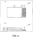
- FIG. 4 shows that in such electronic components, a structure of a liquid crystal display device (LCD) that is generally used as a small display device suitable for, for example, a clinical thermometer or a mobile instrument such as a smart phone.
- LCD liquid crystal display device
- an LCD 100 includes a color filter substrate 110 for forming an image, an array substrate 130 on which active elements such as a TFT or electrodes serving as subpixels are formed in an array form, and a liquid crystal layer 120 that is provided between these substrates and includes a flowable liquid crystal material.
- Power for driving the LCD 100 is supplied by wiring an external drive circuit to a connection electrode 131 exposed at an end of the array substrate 130. Therefore, the array substrate 130 is larger than the color filter substrate 110 by an exposed area of the connection electrode 131.
- the color filter substrate 110 and the liquid crystal layer 120 are mounted in a convex shape on the array substrate 130 and the LCD 100 has a shape with a step difference near the connection electrode 131.
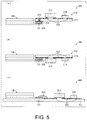
- an electronic device 200 includes the LCD 100 and a drive circuit substrate 210, wherein a drive circuit on which a drive IC 213, a chip component 214, and the like are mounted is formed on a wiring circuit 212 that is formed on a printed wiring substrate 211 including glass epoxy or a flexible substrate (for example, a polyimide).
- the wiring circuit 212 is connected to a back electrode 216 on a back surface of the printed wiring substrate 211 through a through-hole 215.
- a bonding member 220 such as an anisotropic conductive adhesive
- an electronic device 300 has a configuration similar to that of the electronic device 200. That is, the electronic device 300 includes a drive circuit substrate 310 having a configuration wherein the drive circuit substrate 210 is inverted upside down, and has a structure in which a wiring circuit 312 formed on a printed wiring substrate 311 of the drive circuit substrate 310 and the connection electrode 131 of the LCD 100 face each other and these are bonded to each other using the bonding member 220. According to the electronic device 300, there is no need to form the through-hole 215 and the back electrode 216 on the drive circuit substrate 310, and it is possible to reduce manufacturing costs.
- FIG. 5(c) As an electronic device that addresses such problems, an electronic device shown in FIG. 5(c) is known.
- an electronic device 400 has a configuration on which the LCD 100, the drive IC 213, the chip component 214, and the like are mounted on a single printed wiring substrate 411.
- a wiring circuit 412 constituting the drive circuit and the connection electrode 131 of the LCD 100 are connected to each other using a conductive member 420 made of solder or the like. Therefore, it is possible to simplify the manufacturing process of the electronic device 400.
- Patent Literature 1 Japanese Unexamined Patent Application Publication No. 2004-206120 (published July 22, 2004 ).
- the printed wiring substrate 411 is enlarged, and thus there is a limit in dealing with a problem of an increase in size of the manufacturing device. Moreover, there are the following problems.
- a step difference corresponding to the thickness of the array substrate 130 of the LCD 100 is provided between the connection electrode 131 and the wiring circuit 412.
- a plurality of connection electrodes 131 are provided, for example, at a pitch of 1 mm. Therefore, under a condition in which the step difference is provided, when the connection electrode 131 and the wiring circuit 412 are connected, there are problems in that there is a high likelihood of the conductive member 420 being bridged and the reliability of connection decreasing.
- a space and device are still necessary to perform a bonding process and manufacturing costs are high.
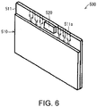
- an array substrate 511 of an LCD 510 is enlarged, and a driver element 520 such as a drive IC and a chip component is mounted on the array substrate 511.
- connection to an external circuit is performed by a connection terminal 511a formed on the back surface of the array substrate 511.
- a color filter and a liquid crystal layer which are constituent members of the LCD 510, and the driver element 520. Therefore, it is not possible to use mass-produced inexpensive general-purpose components and there is a problem of manufacturing costs increasing.
- a small terminal such as a wearable product, it is difficult to obtain a profit without lowering manufacturing costs, and reduction in manufacturing costs becomes very important.
- the present invention has been made in view of the above problems in the related art, and an object of the present invention is to provide an electronic device, wherein a first electronic component having a shape with a step difference near an external connection terminal and a second electronic component associated with an operation of the first electronic component are connected by a wiring so that it is possible to avoid an increase in size of the manufacturing device and it is possible to perform wiring at low cost, and it is possible to increase the reliability of wiring connection and a method of manufacturing the same.
- the electronic device is an electronic device, wherein a first electronic component in which an upper member is mounted in a convex shape on a wiring substrate having an external connection terminal and a second electronic component associated with an operation of the first electronic component are connected by a wiring, and the first electronic component and the second electronic component are exposed so that an external connection terminal of the first electronic component and an electrode of the second electronic component are positioned on the same surface and are embedded in a resin molded body.
- the present invention has an effect of providing an electronic device wherein a first electronic component having a shape with a step difference near an external connection terminal and a second electronic component associated with an operation of the first electronic component are connected by a wiring, so that it is possible to avoid an increase in size of the manufacturing device and it is possible to perform wiring at low cost, and it is possible to increase the reliability of wiring connection and a method of manufacturing the same.
- LCD liquid crystal display device
- the electronic device of the present invention is not limited thereto.
- the present invention can be applied to mounting of an electronic component having a shape with a step difference near an external connection terminal.
- the present invention can be applied to an electronic device such as a portable electronic instrument, a small sensor, or a healthcare instrument such as an electronic thermometer and a sphygmomanometer in addition to a liquid crystal display device (LCD), and a method of manufacturing the same.
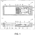
- FIG. 1(a) is a plan view showing a schematic configuration of an electronic device according to Embodiment 1 of the present invention and FIG. 1(b) is a side cross-sectional view.
- the electronic device 1A of the present embodiment includes an LCD 10 which is a first electronic component, an IC 20 and a chip component 21 which are second electronic components associated with an operation of the LCD 10, and a resin molded body 30 that is formed to fix the components.
- the LCD 10, the IC 20, and the chip component 21 are connected by a wiring.
- the LCD 10 includes a color filter substrate 11 for forming an image, an array substrate 13 on which active elements such as a TFT or display electrodes serving as subpixels are formed in an array form (arrangement), and a liquid crystal layer 12 that is provided between the color filter substrate 11 and the array substrate 13 and includes a flowable liquid crystal material.
- the LCD 10 of the present embodiment is assumed to be a reflective type, the present invention is not necessarily limited thereto, and a backlight type may be used.
- the color filter substrate 11 for color display is provided.
- the present invention is not necessarily limited thereto, and a monochrome display may be used.
- an upper substrate such as a glass substrate is provided as a protective member.
- the array substrate 13 has a larger area than the color filter substrate 11 and the liquid crystal layer 12. At an end of the array substrate 13, a connection electrode 13a as an external connection terminal that is exposed to the outside is provided. When an external drive circuit is connected to the connection electrode 13a by wiring, power for driving the LCD 10 is supplied.
- the LCD 10 is an electronic component having a shape with a step difference.
- the LCD 10 includes a thick part 10a having a relatively large thickness and a thin part 10b having a relatively thin thickness, and a first step portion 10c that is provided at a boundary between the thick part 10a and the thin part 10b.
- the thick part 10a is a part on which the color filter substrate 11 and the liquid crystal layer 12 as upper members are mounted in a convex shape on the array substrate 13, and the thin part 10b is a part on which no upper member is provided.
- the thick part 10a functions as an image display unit of the LCD 10.
- the LCD 10 includes a second step portion 10d making up the thickness of the array substrate 13.
- the IC 20 is an electronic component for controlling and driving the LCD 10
- the chip component 21 is an electronic component such as a resistor and a capacitor.
- the second electronic components such as the IC 20 and the chip component 21 are not limited thereto, and, for example, a passive component (such as a resistor and a capacitor), an active component (such as an LSI and an IC), a power supply device (such as a battery), a display device (such as an LED), or other electronic components (such as a sensor and a switch) may be used.
- a plurality of ICs 20 and chip components 21 may be provided.
- An IC electrode (not shown) is provided on a surface of the IC 20, and a chip component electrode (not shown) is provided on a surface of the chip component 21.
- a plurality of IC electrodes and chip component electrodes may be provided.
- the resin molded body 30 is made of a resin such as polycarbonate (PC) or acrylonitrile butadiene styrene (ABS) and is a rectangular resin molded body having a hole 31 provided therein.
- the resin constituting the resin molded body 30 is not limited thereto.
- a bottom surface of the hole 31 is defined as a hole bottom surface 31a.
- the resin molded body 30 covers a side surface and a bottom surface of the IC 20, and a surface of the IC 20 and the IC electrode are exposed from the hole bottom surface 31a. Similarly, the resin molded body 30 covers a side surface and a bottom surface of the chip component 21 and a surface of the chip component 21 and the chip component electrode are exposed from the hole bottom surface 31a.
- the resin molded body 30 covers a side surface of the array substrate 13 in the LCD 10 and covers at least a part of the bottom surface. Then, among four surfaces which are side surfaces of the color filter substrate 11 and the liquid crystal layer 12, the resin molded body 30 covers three surfaces other than a surface on the side in which the connection electrode 13a is provided on the array substrate 13.
- the resin molded body 30 is formed in a concave shape and covers a peripheral part of the electronic device 1A, it is possible to improve the mechanical strength of the electronic device 1A.
- the hole bottom surface 31a may have a flat surface shape, and may be bent and have a plurality of flat surfaces, or have a gently curved surface.
- the shape of the resin molded body 30 is not limited to a rectangular shape and may be other shapes.
- an opening 32 is formed in an area of the thick part 10a of the LCD 10 on which an upper member is provided. Therefore, display towards the back surface of the electronic device 1A, that is, the lower side in FIG. 1(b) is made possible.
- the opening 32 is not essential for the configuration, but it may be provided as necessary.
- the resin molded body 30 is formed to cover a peripheral part of the exposed back surface 13b.
- the resin molded body 30 covers a bottom edge and a peripheral part of the array substrate 13 of the area of the thick part 10a, which is an area in which the upper member is provided. That is, an area of the exposed back surface 13b is smaller than an area of the array substrate 13 of the area of the thick part 10a.
- a part covered with the resin molded body 30 at the bottom edge and the peripheral part of the array substrate 13 of the area of the thick part 10a is defined as a resin-covered part 14.
- the bottom edge of the array substrate 13 of the area of the thick part 10a is a part on the bottom side at a corner between a bottom surface and a side surface of the array substrate 13.
- the peripheral part of the array substrate 13 of the area of the thick part 10a is a side surface part of the array substrate 13.
- an electronic component having a shape including the first step portion 10c and the second step portion 10d near the connection electrode 13a of the LCD 10 is mounted so that the connection electrode 13a, the IC electrode, and the chip component electrode are on the same surface as the hole bottom surface 31a.
- the same surface is a circuit formation surface.
- the circuit formation surface has no step difference for preventing circuit formation.
- the circuit formation surface may be flat to an extent at which it is possible to form a circuit including the connection electrode 13a, the IC electrode, and the chip component electrode by print printing using an ink jet printer on the circuit formation surface.
- a conductive material for example, a conductive ink such as a silver ink
- an ink jet printer or the like it is possible to form a wiring circuit 22 on the circuit formation surface at low cost.
- a metal wiring for example, a metal wiring.
- the wiring circuit 22 can be formed on the circuit formation surface, it is possible to increase the reliability of connection. That is, even if connection electrodes 13a with a narrow pitch are wired, the likelihood of a wiring being bridged is reduced.
- a printed wiring substrate and a conductive member in the related art are not necessary, and a bonding process in which a drive circuit of the printed wiring substrate and the connection electrode 13a are bonded to each other using a conductive member is not necessary. Therefore, it is not necessary to secure a space necessary for the bonding process, and it is possible to prevent the size of a manufacturing device from increasing and manufacturing costs from increasing.
- the wiring circuit 22 can be formed when positions of the connection electrode 13a, the IC electrode, and the chip component electrode are determined, and can be easily wired accurately.
- the LCD 10, the IC 20, and the chip component 21 are fixed by the resin molded body 30 and the wiring circuit 22 is also formed on the circuit formation surface. Therefore, it is possible to reduce problems such as deformation or damage of the wiring circuit 22 and insufficient bonding strength of the wiring.
- connection electrode 13a, the IC 20, and the chip component 21 can be wired in a desired combination on the circuit formation surface.
- the electronic device 1A of the present embodiment includes the resin-covered part 14. Therefore, since the peripheral part of the exposed back surface 13b is covered with a resin, it is possible to prevent water or the like from entering a side surface of the LCD 10 from the opening 32.
- a waterproof property is important for products such as a clinical thermometer and a wearable terminal installed in clothes, and the present invention can be suitably used for such products.
- the resin molded body 30 may have a reduced area that is adhered to the LCD 10 due to thermal contraction after resin molding in the manufacturing process.
- the electronic device 1A of the present embodiment includes the resin-covered part 14, adhesion between the resin molded body 30 and the LCD 10 is easily maintained. As a result, fixation of the LCD 10 by the resin molded body 30 is promoted, and the mechanical strength is improved.
- the shape and the depth of the hole 31 can be changed according to the shape and the height of the first electronic component and the second electronic component, it is possible to freely select the first electronic component and the second electronic component. Therefore, it is possible to use an inexpensive and mass-produced electronic component that is generally commercially available. Therefore, it is possible to reduce manufacturing costs of the electronic device.
- the depth of the hole 31 of the resin molded body 30 is preferably, for example, about 3 mm or less.
- a distance between the circuit formation surface and a nozzle of the ink jet printer or the like is about 3 mm or less, it is possible to suitably form a printed circuit. Therefore, when the nozzle is relatively moved directly above the electronic device, it is possible to form a printed circuit.
- a distance is too long, it is necessary for a tip of the nozzle to enter the hole 31. In this case, since it is necessary to move the nozzle up and down, in a plurality of electronic devices 1A, a time required when printed circuits are continuously formed on the electronic devices 1A increases.
- the hole bottom surface 31a of the resin molded body 30 is a circuit formation surface, but the electronic device of the present invention is not limited thereto. That is, the hole 31 may not be formed in the resin molded body 30.
- the connection electrode 13a, the IC electrode, and the chip component electrode are on the same surface, and may form a circuit formation surface.
- FIG. 2(a), (b), (c), (d), and (e) are side cross-sectional views explaining an example of a method of manufacturing the electronic device of the present embodiment.
- a film 41 (sheet member) is fixed to surfaces of the first surface 40a and the second surface 40b of a jig 40 including a first surface 40a and a second surface 40b whose heights are different from each other (preliminary preparation process).
- the second surface 40b has the same shape as a shape of the hole bottom surface 31a of the resin molded body 30 to be manufactured.
- the same shape does not mean the same without any difference in size and includes substantially the same shape. That is, there may be slight differences due to thermal expansion, thermal contraction, or the like, and this applies similarly in the following description.
- the film 41 for example, polyethylene terephthalate (PET), polyethylene naphthalate (PEN), and polyphenylene sulfide (PPS) can be used. According to reasons which will follow, the film 41 is preferably made of a flexible material through which ultraviolet rays pass.
- PET polyethylene terephthalate
- PEN polyethylene naphthalate
- PPS polyphenylene sulfide
- the film 41 may be a carrier tape, a glass epoxy substrate, or the like.
- a material of the film 41 is not particularly limited as long as it is capable of temporarily fixing an electronic component and can be peeled off after the electronic device 1A is manufactured.
- the film 41 of the first surface 40a is attached to and temporarily fixed to the color filter substrate 11 of the LCD 10.
- the connection electrode 13a of the array substrate 13, an IC electrode 20a, and a chip component electrode 21a are attached and temporarily fixed to the film 41 of the second surface 40b so that they are in contact with the film 41 of the second surface 40b (attachment and temporary fixation process).
- the temporary fixation can be performed using, for example, an ultraviolet curable adhesive (not shown) that is applied to one surface of the film 41.
- an ultraviolet curable adhesive (not shown) that is applied to one surface of the film 41.
- GL-3005H commercially available from Gluelabo
- the adhesive may be applied at a thickness of 2 ⁇ m to 3 ⁇ m to, for example, a50 ⁇ m film 41 made of PET.
- the LCD 10, the IC 20, and the chip component 21 are positioned and installed.
- ultraviolet rays having an intensity of 3000 mJ/cm 2 are emitted, the adhesive is cured, and the LCD 10, the IC 20, and the chip component 21 are temporarily fixed to the film 41.
- the ultraviolet rays are preferably emitted from the side of the jig 40. This is because, when ultraviolet rays are emitted from the side to which electronic components such as the LCD 10 are temporarily fixed, ultraviolet curing may be insufficient in parts in the shadow of such electronic components and the like. In this case, temporary fixation is insufficient.
- the jig 40 is preferably made of a material through which ultraviolet rays pass, for example, glass, transparent polycarbonate (PC), acrylic, or the like.
- a material through which ultraviolet rays pass for example, glass, transparent polycarbonate (PC), acrylic, or the like.
- one continuous film 41 can be used.
- the film 41 shrinks and bends due to a step difference at the boundary between the first surface 40a and the second surface 40b of the jig 40, positional accuracy of electronic components such as the LCD 10 to be temporarily fixed may decrease. Therefore, as in the present embodiment, preferably, the film 41 is separated into a first film 41a used for the first surface 40a and a second film 41b used for the second surface 40b.
- the film 41 to which electronic components such as the LCD 10 are temporarily fixed is removed from the jig 40.
- the film 41 to which electronic components such as the LCD 10 are temporarily fixed is disposed and accommodated inside a mold 50 for manufacturing the resin molded body 30 (mold accommodation process), and resin molding is performed so that the electronic components that are temporarily fixed are embedded in the resin molded body 30 (resin molding process).
- the mold 50 is a metal mold for injection molding the resin molded body 30 and includes a first mold 51 and a second mold 52.
- the first mold 51 has a first surface 51a and a second surface 51b whose heights are different from each other as two surfaces corresponding to the jig 40.
- a surface of the first film 41a that is in contact with the jig 40 is disposed on the first surface 51a of the first mold 51.
- a surface of the second film 41b that is in contact with the jig 40 is disposed on the second surface 51b of the first mold 51.
- the second mold 52 includes a convex part 52a corresponding to the shape of the opening 32.
- an area of a surface of the convex part 52a is set to be smaller than the thick part 10a of the LCD 10, after resin molding, the resin-covered part 14 can be formed on a peripheral part of the exposed back surface 13b of the LCD.
- Conditions in which injection molding is performed may be appropriately selected according to the resin constituting the resin molded body 30.
- PC polycarbonate
- ABS acrylonitrile butadiene styrene
- injection molding is performed at an injection resin temperature of 180 °C and an injection pressure of 20 kgf/cm 2 .
- Various resin materials can be used for the resin constituting the resin molded body 30.
- conditions in which injection molding is performed are not particularly limited.
- the resin molded body 30 in which the LCD 10, the IC 20, and the chip component 21 are embedded is removed from the mold 50, and the film 41 is separated therefrom (removal process). Therefore, the electronic device 1A can be obtained.
- the film 41 when a material, for example, a PET film, is used as the film 41, since the PET film changes greatly due to a thermal change in the resin molding process, the film 41 easily separates off. This is because the film 41 that is greatly deformed due to thermal expansion and thermal contraction spontaneously separates from electronic components such as the LCD 10.
- a material for example, a PET film
- connection electrode 13a the connection electrode 13a, the IC electrode, and the chip component electrode which are exposed to the hole bottom surface 31a are wired and connected by, for example, print printing (wiring connection process).
- the print printing can be performed by a method of printing by spraying a conductive material (for example, a silver ink) using, for example, an ink jet printer.
- a conductive material for example, a silver ink
- the depth of the hole 31 of the electronic device 1A of the present embodiment is about 3 mm or less.
- the nozzle is relatively moved directly above the electronic device 1A and the wiring circuit 22 can be formed on the hole bottom surface 31a.
- Embodiment 1 Another embodiment of the present invention will be described below with reference to FIG. 3 .
- the configuration other than that described in the present embodiment is the same as in Embodiment 1.
- members having the same functions as members shown in the drawings in Embodiment 1 are denoted with the same reference numerals, and descriptions thereof will be omitted.
- the electronic device 1A of Embodiment 1 an electronic device on which the LCD 10 as an electronic component having a shape with a step difference near an electrode part for electrical wiring is mounted has been exemplified.
- the electronic device of the present Embodiment 2 is an electronic device on which a substrate module (for example, wireless communication, various sensors, and switches) as an electronic component is mounted, which is different from the electronic device 1A of Embodiment 1.
- FIG. 3(a) is a plan view showing a configuration of a module substrate in Embodiment 2 of the present invention
- FIG. 3(b) is a side cross-sectional view.
- a substrate module 60 mounted on the electronic device 1B of the present embodiment includes an IC 62, a chip component 63, and an electromagnetic shield 64 as a protective member covering them, which are mounted on a printed substrate 61 as a wiring substrate.
- the substrate module 60 is an electronic component having a shape with a step difference. That is, the substrate module 60 includes a thick part 60a having a relatively large thickness and a thin part 60b having a relatively thin thickness, and a first step portion 60c that is provided at a boundary between the thick part 60a and the thin part 60b.
- the thick part 60a is a part on which the electromagnetic shield 64 is provided on the printed substrate 61 and the thin part 60b is a part on which the electromagnetic shield 64 is not provided.
- the substrate module 60 includes a second step portion 60d making up the thickness of the printed substrate 61.
- the printed substrate 61 includes a wiring circuit 61a on its surface. At an end of the printed substrate 61, a connection electrode 61b that is exposed to the outside and is connected to the inside of the electromagnetic shield 64 is provided. When an external drive circuit is wired to the connection electrode 61b, power for driving the substrate module 60 is supplied.
- the electronic device 1B can be obtained. Specifically, in the electronic device 1B, the connection electrode 61b, the IC electrode, and the chip component electrode are on the same surface as the surface of the resin molded body. Therefore, it is possible to provide an electronic device having the same operations and effects as in the electronic device 1A.
- the electronic device is an electronic device in which the first electronic component in which an upper member is mounted in a convex shape on a wiring substrate including an external connection terminal and the second electronic component associated with an operation of the first electronic component are connected by a wiring, and the first electronic component and the second electronic component are exposed so that an external connection terminal of the first electronic component and an electrode of the second electronic component are positioned on the same surface and are embedded in the resin molded body.
- the external connection terminal of the first electronic component and the electrode of the second electronic component are on the same surface. Therefore, using a simple method such as print printing using, for example, an ink jet printer, it is possible to perform wiring at low cost.
- a conductive adhesive for connecting electrodes or the like is not necessary, and the bonding process can be omitted. Therefore, it is possible to reduce manufacturing costs. Thus, since it is not necessary to secure a space for performing such a bonding process, it is possible to prevent the size of the device from increasing.
- the first electronic component and the second electronic component are fixed to the resin molded body and the wiring circuit can be formed on the resin molded body without generating a step difference. As a result, it is possible to increase the mechanical strength.
- the first electronic component is preferably embedded in the resin molded body so that the external connection terminal of the first electronic component and the electrode of the second electronic component are aligned on the same surface.
- the first electronic component is embedded in the resin molded body so that the external connection terminal of the first electronic component and the electrode of the second electronic component are aligned on the same surface.
- the wiring substrate of the first electronic component is embedded in the resin molded body to an extent of the step difference, such that even though such a step difference is provided, it is possible to align the external connection terminal of the first electronic component and the electrode of the second electronic component on the same surface.
- a plurality of second electronic components are provided, and any electrode of the plurality of second electronic components may be on the same surface as the surface of the resin molded body.
- the external connection terminal and the electrode of the second electronic components on the same surface as the surface of the resin molded body.
- the plurality of second electronic components can be wired on the same surface as the surface of the resin molded body.
- the resin molded body has an opening that is formed in an area in which the upper member is provided and may cover a bottom edge of the upper member.
- the resin molded body has an opening that is formed in an area in which the upper member is provided. Therefore, when the electronic device is a liquid crystal display device, it is possible to perform display on the side of the array substrate which is a wiring substrate.
- the bottom edge of the upper member is covered with a resin, it is possible to prevent water or the like from entering a side surface of the first electronic component from the opening. Therefore, it is possible to prevent a failure of the first electronic component due to water or the like.
- the mechanical strength of the electronic device can be improved.
- the first electronic component is a liquid crystal display device
- the wiring substrate is an array substrate in which display electrodes are formed in an array shape
- the upper member may include an upper substrate and a liquid crystal layer that is provided between the upper substrate and the array substrate and includes a liquid crystal material.
- the present invention can be suitably used for small products for which a waterproof property is required such as a clinical thermometer and a wearable terminal installed in clothes.
- a waterproof property such as a clinical thermometer and a wearable terminal installed in clothes.
- an electronic device including a liquid crystal display device.
- the first electronic component is a substrate module
- the upper member may include a mounted electronic component mounted on the wiring substrate and a protective member covering the mounted electronic component
- a substrate module having various functions in the shape with a step difference near an external connection terminal can be mounted so that the external connection terminal and the electrode of the second electronic component are on the same surface. Therefore, it is possible to perform wiring at low cost and it is possible to increase the reliability of wiring connection. As a result, it is possible to provide an electronic device including a substrate module.
- the external connection terminal of the first electronic component and the electrode of the second electronic component may be connected by a wiring on the surface of the resin molded body.
- the wiring connection is performed without a step difference. Therefore, bridging of the wiring is unlikely to occur, the reliability of connection increases, and even if the resin molded body receives a deforming force for such as expanding, contraction, bending, or the like, the wiring does not easily break. Accordingly, it is possible to provide an electronic device having a wiring with a high degree of reliability.
- the wiring connection may be formed by print printing a conductive material.
- wiring connection can be easily formed using a device such as an ink jet printer.
- a method of manufacturing an electronic device is a method of manufacturing an electronic device, wherein a first electronic component in which an upper member is mounted in a convex shape on a wiring substrate having an external connection terminal and a second electronic component associated with an operation of the first electronic component are connected by a wiring.
- the method includes a preliminary preparation process in which, using a jig having a step difference corresponding to a height of the upper member with a convex shape, a sheet member is fixed to a first surface and a second surface of the jig; an attachment and temporary fixation process in which the upper member is attached to the sheet member of the first surface of the jig and the external connection terminal of the wiring substrate and the second electronic component are attached and temporarily fixed to the sheet member of the second surface of the jig; a mold accommodation process in which the sheet member after the attachment and temporary fixation process is removed from the jig while the first electronic component and the second electronic component are temporarily fixed, and is attached to the inside of an upper mold and accommodated; and a resin molding process in which resin molding is performed so that the first electronic component and the second electronic component are embedded between the upper mold and a lower mold.
- the first electronic component and the second electronic component are temporarily fixed to the sheet member attached to the jig, and the jig is then removed, and attached to the upper mold, and a resin is injected between the upper mold and the lower mold and molded.
- a resin is injected between the upper mold and the lower mold and molded.
- the first electronic component having a shape with a step difference near an external connection terminal and the second electronic component associated with an operation of the first electronic component are connected by a wiring, it is possible to avoid an increase in size of the manufacturing device and it is possible to perform wiring at low cost, and it is possible to provide a method of manufacturing an electronic device capable of increasing the reliability of wiring connection.
- the sheet member may be separated into at least two members including one member that is used for the first surface and one member that is used for the second surface.
- the sheet member does not shrink and bend due to a step difference at the boundary between the first surface and the second surface of the jig. As a result, a likelihood of decreased positional accuracy of the first electronic component and the second electronic component is reduced.
- the method of manufacturing an electronic device may include a removal process in which, after the resin molding process, the first electronic component, the second electronic component, and the resin molded body that is resin-molded are removed, and the sheet member is separated from the first electronic component, the external connection terminal, and the second electronic component; and a wiring connection process in which the external connection terminal and the electrode of the second electronic component which are on the same surface as the surface of the resin molded body are connected by a wiring.
- a conductive ink may be sprayed to print the wiring.
- the first electrode and the electrode of the second electronic component are on the same surface as the surface of the resin molded body, and it is possible to form a circuit by wiring using a simple method in which a conductive material for an inkjet or the like is injected for printing. Therefore, compared to a method in which a wiring is formed using etching or the like, material costs and processing costs can be reduced to low prices.
- conductive material is injected for printing, generally, it is easy to adjust a printing position. As a result, even if the position of the electronic component is deviated from a predetermined position, it is possible to form a wiring according to the deviation.
Landscapes
- Engineering & Computer Science (AREA)
- Physics & Mathematics (AREA)
- Microelectronics & Electronic Packaging (AREA)
- Nonlinear Science (AREA)
- Chemical & Material Sciences (AREA)
- Manufacturing & Machinery (AREA)
- General Physics & Mathematics (AREA)
- Crystallography & Structural Chemistry (AREA)
- Mathematical Physics (AREA)
- Optics & Photonics (AREA)
- Dispersion Chemistry (AREA)
- Liquid Crystal (AREA)
- Devices For Indicating Variable Information By Combining Individual Elements (AREA)
- Structures Or Materials For Encapsulating Or Coating Semiconductor Devices Or Solid State Devices (AREA)
- Health & Medical Sciences (AREA)
- Electromagnetism (AREA)
- Toxicology (AREA)
Abstract
Description
- The present invention relates to an electronic device, wherein a first electronic component in which an upper member is mounted in a convex shape on a wiring substrate having an external connection terminal and a second electronic component associated with an operation of the first electronic component are connected by a wiring, and a method of manufacturing the same.
- In recent years, there has been increasing demand for realizing portable electronic instruments, small sensors, or healthcare instruments (such as an electronic thermometer and a sphygmomanometer) as thin, light, compact, and highly water resistant wearable products at a low cost.
- Generally, such electronic instruments are constructed by incorporating a passive component (such as a resistor and a capacitor), an active component (such as an LSI and an IC), a power supply device (such as a battery), a display device (such as an LED), or other electronic components (such as a sensor and a switch) into a printed wiring substrate.
-
FIG. 4 shows that in such electronic components, a structure of a liquid crystal display device (LCD) that is generally used as a small display device suitable for, for example, a clinical thermometer or a mobile instrument such as a smart phone. - As shown in
FIG. 4(a) and (b) , anLCD 100 includes acolor filter substrate 110 for forming an image, anarray substrate 130 on which active elements such as a TFT or electrodes serving as subpixels are formed in an array form, and aliquid crystal layer 120 that is provided between these substrates and includes a flowable liquid crystal material. Power for driving theLCD 100 is supplied by wiring an external drive circuit to aconnection electrode 131 exposed at an end of thearray substrate 130. Therefore, thearray substrate 130 is larger than thecolor filter substrate 110 by an exposed area of theconnection electrode 131. As a result, in theLCD 100, thecolor filter substrate 110 and theliquid crystal layer 120 are mounted in a convex shape on thearray substrate 130 and theLCD 100 has a shape with a step difference near theconnection electrode 131. - In the related art, as an electronic device in which an electronic component having a step difference near an electrode part such as the
LCD 100 and an external drive circuit are connected to each other, an electronic device shown inFIG. 5(a) and (b) is known. - As shown in
FIG. 5(a) , anelectronic device 200 includes theLCD 100 and adrive circuit substrate 210, wherein a drive circuit on which adrive IC 213, achip component 214, and the like are mounted is formed on awiring circuit 212 that is formed on a printedwiring substrate 211 including glass epoxy or a flexible substrate (for example, a polyimide). Thewiring circuit 212 is connected to aback electrode 216 on a back surface of the printedwiring substrate 211 through a through-hole 215. When theback electrode 216 and theconnection electrode 131 of theLCD 100 are bonded to each other using abonding member 220 such as an anisotropic conductive adhesive, theLCD 100 and the drive circuit are connected to each other. - As shown in
FIG. 5(b) , anelectronic device 300 has a configuration similar to that of theelectronic device 200. That is, theelectronic device 300 includes adrive circuit substrate 310 having a configuration wherein thedrive circuit substrate 210 is inverted upside down, and has a structure in which awiring circuit 312 formed on a printedwiring substrate 311 of thedrive circuit substrate 310 and theconnection electrode 131 of theLCD 100 face each other and these are bonded to each other using thebonding member 220. According to theelectronic device 300, there is no need to form the through-hole 215 and theback electrode 216 on thedrive circuit substrate 310, and it is possible to reduce manufacturing costs. - However, in the
electronic device 200 and theelectronic device 300, in processes of manufacturing these components, a space for installing thebonding member 220, a space for performing a bonding process, and the like are necessary. Therefore, there are problems in that the size of a manufacturing device increases, bonding operations are complicated, and manufacturing costs increase. In addition, in order to deal with a problem related to the reliability such as insufficient bonding strength, there is a problem in which another member is necessary to prevent deformation of a bonding part. - As an electronic device that addresses such problems, an electronic device shown in
FIG. 5(c) is known. - As shown in
FIG. 5(c) , anelectronic device 400 has a configuration on which theLCD 100, thedrive IC 213, thechip component 214, and the like are mounted on a single printedwiring substrate 411. Awiring circuit 412 constituting the drive circuit and theconnection electrode 131 of theLCD 100 are connected to each other using aconductive member 420 made of solder or the like. Therefore, it is possible to simplify the manufacturing process of theelectronic device 400. - [Patent Literature 1] Japanese Unexamined Patent Application Publication No.
2004-206120 (published July 22, 2004 - However, in the
electronic device 400, the printedwiring substrate 411 is enlarged, and thus there is a limit in dealing with a problem of an increase in size of the manufacturing device. Moreover, there are the following problems. - A step difference corresponding to the thickness of the
array substrate 130 of theLCD 100 is provided between theconnection electrode 131 and thewiring circuit 412. In addition, generally, a plurality ofconnection electrodes 131 are provided, for example, at a pitch of 1 mm. Therefore, under a condition in which the step difference is provided, when theconnection electrode 131 and thewiring circuit 412 are connected, there are problems in that there is a high likelihood of theconductive member 420 being bridged and the reliability of connection decreasing. In addition, since it is necessary to fix members using a thermocompression sheet or the like, a space and device are still necessary to perform a bonding process and manufacturing costs are high. - As shown in
FIG. 6 , as another electronic device, in adisplay module 500 disclosed in Patent Literature 1, anarray substrate 511 of anLCD 510 is enlarged, and adriver element 520 such as a drive IC and a chip component is mounted on thearray substrate 511. In addition, connection to an external circuit is performed by aconnection terminal 511a formed on the back surface of thearray substrate 511. However, in such an electronic device, it is necessary to mount and process simultaneously a color filter and a liquid crystal layer which are constituent members of theLCD 510, and thedriver element 520. Therefore, it is not possible to use mass-produced inexpensive general-purpose components and there is a problem of manufacturing costs increasing. In particular, in such a small terminal such as a wearable product, it is difficult to obtain a profit without lowering manufacturing costs, and reduction in manufacturing costs becomes very important. - The present invention has been made in view of the above problems in the related art, and an object of the present invention is to provide an electronic device, wherein a first electronic component having a shape with a step difference near an external connection terminal and a second electronic component associated with an operation of the first electronic component are connected by a wiring so that it is possible to avoid an increase in size of the manufacturing device and it is possible to perform wiring at low cost, and it is possible to increase the reliability of wiring connection and a method of manufacturing the same.
- In order to address the above problems, the electronic device according to an embodiment of the present invention is an electronic device, wherein a first electronic component in which an upper member is mounted in a convex shape on a wiring substrate having an external connection terminal and a second electronic component associated with an operation of the first electronic component are connected by a wiring, and the first electronic component and the second electronic component are exposed so that an external connection terminal of the first electronic component and an electrode of the second electronic component are positioned on the same surface and are embedded in a resin molded body.
- The present invention has an effect of providing an electronic device wherein a first electronic component having a shape with a step difference near an external connection terminal and a second electronic component associated with an operation of the first electronic component are connected by a wiring, so that it is possible to avoid an increase in size of the manufacturing device and it is possible to perform wiring at low cost, and it is possible to increase the reliability of wiring connection and a method of manufacturing the same.
-
-
FIG. 1(a) is a plan view showing a schematic configuration of an electronic device according to Embodiment 1 of the present invention and (b) is a side cross-sectional view. -
FIG. 2(a), (b), (c), (d), and (e) are side cross-sectional views explaining an example of a method of manufacturing the electronic device. -
FIG. 3(a) is a plan view showing a configuration of an electronic device according to Embodiment 2 of the present invention and (b) is a side cross-sectional view. -
FIG. 4(a) is a plan view showing a schematic configuration of a liquid crystal display device of the related art, and (b) is a side cross-sectional view. -
FIG. 5 is a side cross-sectional view showing a schematic configuration of an electronic device of the related art. -
FIG. 6 is a perspective view showing a schematic configuration of the electronic device of the related art. - An embodiment of the present invention will be described below with reference to
FIG. 1 andFIG. 2 . - In the present embodiment, as an example of an electronic device of the present invention, an electronic device on which a liquid crystal display device (LCD) is mounted will be described.
- Here, while an electronic device on which a liquid crystal display device (LCD) is mounted will be described as an example of the electronic device in the present embodiment, the electronic device of the present invention is not limited thereto. The present invention can be applied to mounting of an electronic component having a shape with a step difference near an external connection terminal. Specifically, the present invention can be applied to an electronic device such as a portable electronic instrument, a small sensor, or a healthcare instrument such as an electronic thermometer and a sphygmomanometer in addition to a liquid crystal display device (LCD), and a method of manufacturing the same.
- A configuration of an
electronic device 1A according to the present embodiment will be described with reference toFIG. 1(a) and (b). FIG. 1(a) is a plan view showing a schematic configuration of an electronic device according to Embodiment 1 of the present invention andFIG. 1(b) is a side cross-sectional view. - As shown in
FIG. 1(a) and (b) , theelectronic device 1A of the present embodiment includes anLCD 10 which is a first electronic component, anIC 20 and achip component 21 which are second electronic components associated with an operation of theLCD 10, and a resin moldedbody 30 that is formed to fix the components. In theelectronic device 1A, theLCD 10, theIC 20, and thechip component 21 are connected by a wiring. - The
LCD 10 includes acolor filter substrate 11 for forming an image, anarray substrate 13 on which active elements such as a TFT or display electrodes serving as subpixels are formed in an array form (arrangement), and a liquid crystal layer 12 that is provided between thecolor filter substrate 11 and thearray substrate 13 and includes a flowable liquid crystal material. Here, while theLCD 10 of the present embodiment is assumed to be a reflective type, the present invention is not necessarily limited thereto, and a backlight type may be used. In addition, in theLCD 10 of the present embodiment, thecolor filter substrate 11 for color display is provided. However, the present invention is not necessarily limited thereto, and a monochrome display may be used. In this case, generally, instead of thecolor filter substrate 11, an upper substrate such as a glass substrate is provided as a protective member. - The
array substrate 13 has a larger area than thecolor filter substrate 11 and the liquid crystal layer 12. At an end of thearray substrate 13, aconnection electrode 13a as an external connection terminal that is exposed to the outside is provided. When an external drive circuit is connected to theconnection electrode 13a by wiring, power for driving theLCD 10 is supplied. - The
LCD 10 is an electronic component having a shape with a step difference. TheLCD 10 includes athick part 10a having a relatively large thickness and athin part 10b having a relatively thin thickness, and afirst step portion 10c that is provided at a boundary between thethick part 10a and thethin part 10b. - The
thick part 10a is a part on which thecolor filter substrate 11 and the liquid crystal layer 12 as upper members are mounted in a convex shape on thearray substrate 13, and thethin part 10b is a part on which no upper member is provided. Thethick part 10a functions as an image display unit of theLCD 10. - In addition, the
LCD 10 includes asecond step portion 10d making up the thickness of thearray substrate 13. - The
IC 20 is an electronic component for controlling and driving theLCD 10, and thechip component 21 is an electronic component such as a resistor and a capacitor. Here, the second electronic components such as theIC 20 and thechip component 21 are not limited thereto, and, for example, a passive component (such as a resistor and a capacitor), an active component (such as an LSI and an IC), a power supply device (such as a battery), a display device (such as an LED), or other electronic components (such as a sensor and a switch) may be used. In addition, a plurality ofICs 20 andchip components 21 may be provided. - An IC electrode (not shown) is provided on a surface of the
IC 20, and a chip component electrode (not shown) is provided on a surface of thechip component 21. Here, a plurality of IC electrodes and chip component electrodes may be provided. - The resin molded
body 30 is made of a resin such as polycarbonate (PC) or acrylonitrile butadiene styrene (ABS) and is a rectangular resin molded body having ahole 31 provided therein. Here, the resin constituting the resin moldedbody 30 is not limited thereto. - At the bottom of the
hole 31, thearray substrate 13 of theLCD 10, theIC 20, and thechip component 21 are embedded so that electrodes are exposed. Here, a bottom surface of thehole 31 is defined as a holebottom surface 31a. - That is, the resin molded
body 30 covers a side surface and a bottom surface of theIC 20, and a surface of theIC 20 and the IC electrode are exposed from the holebottom surface 31a. Similarly, the resin moldedbody 30 covers a side surface and a bottom surface of thechip component 21 and a surface of thechip component 21 and the chip component electrode are exposed from the holebottom surface 31a. - In addition, the resin molded
body 30 covers a side surface of thearray substrate 13 in theLCD 10 and covers at least a part of the bottom surface. Then, among four surfaces which are side surfaces of thecolor filter substrate 11 and the liquid crystal layer 12, the resin moldedbody 30 covers three surfaces other than a surface on the side in which theconnection electrode 13a is provided on thearray substrate 13. - Accordingly, since the resin molded
body 30 is formed in a concave shape and covers a peripheral part of theelectronic device 1A, it is possible to improve the mechanical strength of theelectronic device 1A. - Here, the hole
bottom surface 31a may have a flat surface shape, and may be bent and have a plurality of flat surfaces, or have a gently curved surface. The shape of the resin moldedbody 30 is not limited to a rectangular shape and may be other shapes. - In addition, in the resin molded
body 30, anopening 32 is formed in an area of thethick part 10a of theLCD 10 on which an upper member is provided. Therefore, display towards the back surface of theelectronic device 1A, that is, the lower side inFIG. 1(b) is made possible. - Here, in the electronic device of the present invention, as described in Embodiment 2 to be described below, application to an electronic device on which a substrate module without the
opening 32 is mounted is possible. Therefore, in the electronic device of the present invention, theopening 32 is not essential for the configuration, but it may be provided as necessary. - When a surface of the
array substrate 13 exposed to the outside through theopening 32 is defined as an exposed backsurface 13b, the resin moldedbody 30 is formed to cover a peripheral part of the exposed backsurface 13b. In other words, the resin moldedbody 30 covers a bottom edge and a peripheral part of thearray substrate 13 of the area of thethick part 10a, which is an area in which the upper member is provided. That is, an area of the exposed backsurface 13b is smaller than an area of thearray substrate 13 of the area of thethick part 10a. A part covered with the resin moldedbody 30 at the bottom edge and the peripheral part of thearray substrate 13 of the area of thethick part 10a is defined as a resin-coveredpart 14. Here, the bottom edge of thearray substrate 13 of the area of thethick part 10a is a part on the bottom side at a corner between a bottom surface and a side surface of thearray substrate 13. The peripheral part of thearray substrate 13 of the area of thethick part 10a is a side surface part of thearray substrate 13. - In the
electronic device 1A of the present embodiment having the above configuration, an electronic component having a shape including thefirst step portion 10c and thesecond step portion 10d near theconnection electrode 13a of theLCD 10 is mounted so that theconnection electrode 13a, the IC electrode, and the chip component electrode are on the same surface as the holebottom surface 31a. The same surface is a circuit formation surface. The circuit formation surface has no step difference for preventing circuit formation. - Here, "on the same surface as the hole
bottom surface 31a" and "has no step difference" do not strictly mean that there is no step difference between the holebottom surface 31a and any of the surface of theconnection electrode 13a, the surface of the IC electrode and the surface of the chip component electrode, that is, the step difference does not need to be completely zero. For example, a minute step difference that is inevitably formed in the manufacturing process is allowed. Specifically, the circuit formation surface may be flat to an extent at which it is possible to form a circuit including theconnection electrode 13a, the IC electrode, and the chip component electrode by print printing using an ink jet printer on the circuit formation surface. - Therefore, for example, using print printing such as injecting a conductive material (for example, a conductive ink such as a silver ink) for wiring using an ink jet printer or the like, it is possible to form a
wiring circuit 22 on the circuit formation surface at low cost. Here, it is possible to form thewiring circuit 22 using another method such as a metal wiring. - In addition, since the
wiring circuit 22 can be formed on the circuit formation surface, it is possible to increase the reliability of connection. That is, even ifconnection electrodes 13a with a narrow pitch are wired, the likelihood of a wiring being bridged is reduced. - Thus, a printed wiring substrate and a conductive member in the related art are not necessary, and a bonding process in which a drive circuit of the printed wiring substrate and the
connection electrode 13a are bonded to each other using a conductive member is not necessary. Therefore, it is not necessary to secure a space necessary for the bonding process, and it is possible to prevent the size of a manufacturing device from increasing and manufacturing costs from increasing. - In addition, the
wiring circuit 22 can be formed when positions of theconnection electrode 13a, the IC electrode, and the chip component electrode are determined, and can be easily wired accurately. - Furthermore, the
LCD 10, theIC 20, and thechip component 21 are fixed by the resin moldedbody 30 and thewiring circuit 22 is also formed on the circuit formation surface. Therefore, it is possible to reduce problems such as deformation or damage of thewiring circuit 22 and insufficient bonding strength of the wiring. - Thus, even if a plurality of
ICs 20 andchip components 21 are provided, electrodes of the plurality ofICs 20 andchip components 21 are on the same surface as the circuit formation surface. Therefore, theconnection electrode 13a, theIC 20, and thechip component 21 can be wired in a desired combination on the circuit formation surface. - In addition, the
electronic device 1A of the present embodiment includes the resin-coveredpart 14. Therefore, since the peripheral part of the exposed backsurface 13b is covered with a resin, it is possible to prevent water or the like from entering a side surface of theLCD 10 from theopening 32. For example, a waterproof property is important for products such as a clinical thermometer and a wearable terminal installed in clothes, and the present invention can be suitably used for such products. - In addition, the resin molded
body 30 may have a reduced area that is adhered to theLCD 10 due to thermal contraction after resin molding in the manufacturing process. However, since theelectronic device 1A of the present embodiment includes the resin-coveredpart 14, adhesion between the resin moldedbody 30 and theLCD 10 is easily maintained. As a result, fixation of theLCD 10 by the resin moldedbody 30 is promoted, and the mechanical strength is improved. - In addition, since the shape and the depth of the
hole 31 can be changed according to the shape and the height of the first electronic component and the second electronic component, it is possible to freely select the first electronic component and the second electronic component. Therefore, it is possible to use an inexpensive and mass-produced electronic component that is generally commercially available. Therefore, it is possible to reduce manufacturing costs of the electronic device. - The depth of the
hole 31 of the resin moldedbody 30 is preferably, for example, about 3 mm or less. When a distance between the circuit formation surface and a nozzle of the ink jet printer or the like is about 3 mm or less, it is possible to suitably form a printed circuit. Therefore, when the nozzle is relatively moved directly above the electronic device, it is possible to form a printed circuit. On the other hand, when a distance is too long, it is necessary for a tip of the nozzle to enter thehole 31. In this case, since it is necessary to move the nozzle up and down, in a plurality ofelectronic devices 1A, a time required when printed circuits are continuously formed on theelectronic devices 1A increases. - In addition, in the
electronic device 1A of the present embodiment, the holebottom surface 31a of the resin moldedbody 30 is a circuit formation surface, but the electronic device of the present invention is not limited thereto. That is, thehole 31 may not be formed in the resin moldedbody 30. In this case, on a surface of the resin moldedbody 30, theconnection electrode 13a, the IC electrode, and the chip component electrode are on the same surface, and may form a circuit formation surface. - A method of manufacturing the
electronic device 1A of the present embodiment will be described below with reference toFIG. 2(a), (b), (c), (d), and (e). FIG. 2(a), (b), (c), (d), and (e) are side cross-sectional views explaining an example of a method of manufacturing the electronic device of the present embodiment. - As shown in
FIG. 2(a) , in the method of manufacturing theelectronic device 1A of the present embodiment, first, a film 41 (sheet member) is fixed to surfaces of thefirst surface 40a and thesecond surface 40b of ajig 40 including afirst surface 40a and asecond surface 40b whose heights are different from each other (preliminary preparation process). - Here, in the
jig 40, thesecond surface 40b has the same shape as a shape of the holebottom surface 31a of the resin moldedbody 30 to be manufactured. - Here, "the same shape" does not mean the same without any difference in size and includes substantially the same shape. That is, there may be slight differences due to thermal expansion, thermal contraction, or the like, and this applies similarly in the following description.
- As a material of the
film 41, for example, polyethylene terephthalate (PET), polyethylene naphthalate (PEN), and polyphenylene sulfide (PPS) can be used. According to reasons which will follow, thefilm 41 is preferably made of a flexible material through which ultraviolet rays pass. - In addition, the
film 41 may be a carrier tape, a glass epoxy substrate, or the like. A material of thefilm 41 is not particularly limited as long as it is capable of temporarily fixing an electronic component and can be peeled off after theelectronic device 1A is manufactured. - As shown in
FIG. 2(b) , next, thefilm 41 of thefirst surface 40a is attached to and temporarily fixed to thecolor filter substrate 11 of theLCD 10. At the same time, theconnection electrode 13a of thearray substrate 13, an IC electrode 20a, and a chip component electrode 21a are attached and temporarily fixed to thefilm 41 of thesecond surface 40b so that they are in contact with thefilm 41 of thesecond surface 40b (attachment and temporary fixation process). - For example, the temporary fixation can be performed using, for example, an ultraviolet curable adhesive (not shown) that is applied to one surface of the
film 41. Specifically, GL-3005H (commercially available from Gluelabo) as the adhesive may be applied at a thickness of 2 µm to 3 µm to, for example,a50 µm film 41 made of PET. Then, theLCD 10, theIC 20, and thechip component 21 are positioned and installed. Then, for example, when ultraviolet rays having an intensity of 3000 mJ/cm2 are emitted, the adhesive is cured, and theLCD 10, theIC 20, and thechip component 21 are temporarily fixed to thefilm 41. - Here, the ultraviolet rays are preferably emitted from the side of the
jig 40. This is because, when ultraviolet rays are emitted from the side to which electronic components such as theLCD 10 are temporarily fixed, ultraviolet curing may be insufficient in parts in the shadow of such electronic components and the like. In this case, temporary fixation is insufficient. - Therefore, the
jig 40 is preferably made of a material through which ultraviolet rays pass, for example, glass, transparent polycarbonate (PC), acrylic, or the like. When both of thejig 40 and thefilm 41 have ultraviolet transmittance, ultraviolet rays are emitted from the side of thejig 40, and the adhesive can be cured on the entire surface. As a result, sufficient temporary fixation can be performed. - In addition, one
continuous film 41 can be used. However, in this case, since thefilm 41 shrinks and bends due to a step difference at the boundary between thefirst surface 40a and thesecond surface 40b of thejig 40, positional accuracy of electronic components such as theLCD 10 to be temporarily fixed may decrease. Therefore, as in the present embodiment, preferably, thefilm 41 is separated into afirst film 41a used for thefirst surface 40a and asecond film 41b used for thesecond surface 40b. - As shown in
FIG. 2(c) , after the attachment and temporary fixation process, thefilm 41 to which electronic components such as theLCD 10 are temporarily fixed is removed from thejig 40. - As shown in
FIG. 2(d) , next, thefilm 41 to which electronic components such as theLCD 10 are temporarily fixed is disposed and accommodated inside amold 50 for manufacturing the resin molded body 30 (mold accommodation process), and resin molding is performed so that the electronic components that are temporarily fixed are embedded in the resin molded body 30 (resin molding process). - The
mold 50 is a metal mold for injection molding the resin moldedbody 30 and includes afirst mold 51 and asecond mold 52. - The
first mold 51 has afirst surface 51a and asecond surface 51b whose heights are different from each other as two surfaces corresponding to thejig 40. - A surface of the
first film 41a that is in contact with thejig 40 is disposed on thefirst surface 51a of thefirst mold 51. A surface of thesecond film 41b that is in contact with thejig 40 is disposed on thesecond surface 51b of thefirst mold 51. - When the
opening 32 is formed in the resin moldedbody 30, thesecond mold 52 includes aconvex part 52a corresponding to the shape of theopening 32. Here, when an area of a surface of theconvex part 52a is set to be smaller than thethick part 10a of theLCD 10, after resin molding, the resin-coveredpart 14 can be formed on a peripheral part of the exposed backsurface 13b of the LCD. - Conditions in which injection molding is performed may be appropriately selected according to the resin constituting the resin molded
body 30. For example, when polycarbonate (PC) is used, injection molding is performed at an injection resin temperature of 270 °C and an injection pressure of 100 MPa. In addition, when acrylonitrile butadiene styrene (ABS) is used, injection molding is performed at an injection resin temperature of 180 °C and an injection pressure of 20 kgf/cm2. - Various resin materials can be used for the resin constituting the resin molded
body 30. In addition, conditions in which injection molding is performed are not particularly limited. - As shown in
FIG. 2(e) , thereafter, the resin moldedbody 30 in which theLCD 10, theIC 20, and thechip component 21 are embedded is removed from themold 50, and thefilm 41 is separated therefrom (removal process). Therefore, theelectronic device 1A can be obtained. - In this case, when a material, for example, a PET film, is used as the
film 41, since the PET film changes greatly due to a thermal change in the resin molding process, thefilm 41 easily separates off. This is because thefilm 41 that is greatly deformed due to thermal expansion and thermal contraction spontaneously separates from electronic components such as theLCD 10. - Thus, when the
wiring circuit 22 is formed in theelectronic device 1A, theconnection electrode 13a, the IC electrode, and the chip component electrode which are exposed to the holebottom surface 31a are wired and connected by, for example, print printing (wiring connection process). - The print printing can be performed by a method of printing by spraying a conductive material (for example, a silver ink) using, for example, an ink jet printer.
- For example, in print printing using an ink jet printer, the depth of the
hole 31 of theelectronic device 1A of the present embodiment is about 3 mm or less. The nozzle is relatively moved directly above theelectronic device 1A and thewiring circuit 22 can be formed on the holebottom surface 31a. - Another embodiment of the present invention will be described below with reference to
FIG. 3 . Here, the configuration other than that described in the present embodiment is the same as in Embodiment 1. In addition, for convenience of explanation, members having the same functions as members shown in the drawings in Embodiment 1 are denoted with the same reference numerals, and descriptions thereof will be omitted. - In the
electronic device 1A of Embodiment 1, an electronic device on which theLCD 10 as an electronic component having a shape with a step difference near an electrode part for electrical wiring is mounted has been exemplified. On the other hand, the electronic device of the present Embodiment 2 is an electronic device on which a substrate module (for example, wireless communication, various sensors, and switches) as an electronic component is mounted, which is different from theelectronic device 1A of Embodiment 1. - A configuration of an electronic device 1B of the present embodiment will be described with reference to
FIG. 3(a) and (b). FIG. 3(a) is a plan view showing a configuration of a module substrate in Embodiment 2 of the present invention, andFIG. 3(b) is a side cross-sectional view. - As shown in
FIG. 3(a) and (b) , asubstrate module 60 mounted on the electronic device 1B of the present embodiment includes anIC 62, achip component 63, and anelectromagnetic shield 64 as a protective member covering them, which are mounted on a printedsubstrate 61 as a wiring substrate. - The
substrate module 60 is an electronic component having a shape with a step difference. That is, thesubstrate module 60 includes athick part 60a having a relatively large thickness and athin part 60b having a relatively thin thickness, and afirst step portion 60c that is provided at a boundary between thethick part 60a and thethin part 60b. - The
thick part 60a is a part on which theelectromagnetic shield 64 is provided on the printedsubstrate 61 and thethin part 60b is a part on which theelectromagnetic shield 64 is not provided. - In addition, the
substrate module 60 includes asecond step portion 60d making up the thickness of the printedsubstrate 61. - The printed
substrate 61 includes awiring circuit 61a on its surface. At an end of the printedsubstrate 61, aconnection electrode 61b that is exposed to the outside and is connected to the inside of theelectromagnetic shield 64 is provided. When an external drive circuit is wired to theconnection electrode 61b, power for driving thesubstrate module 60 is supplied. - When the
LCD 10 is replaced with thesubstrate module 60 in theelectronic device 1A of Embodiment 1 described above, the electronic device 1B can be obtained. Specifically, in the electronic device 1B, theconnection electrode 61b, the IC electrode, and the chip component electrode are on the same surface as the surface of the resin molded body. Therefore, it is possible to provide an electronic device having the same operations and effects as in theelectronic device 1A. - In addition, even if the
substrate module 60 described above is used, it is possible to manufacture the electronic device 1B according to the same manufacturing method as in Embodiment 1. - As described above, the electronic device according to an embodiment of the present invention is an electronic device in which the first electronic component in which an upper member is mounted in a convex shape on a wiring substrate including an external connection terminal and the second electronic component associated with an operation of the first electronic component are connected by a wiring, and the first electronic component and the second electronic component are exposed so that an external connection terminal of the first electronic component and an electrode of the second electronic component are positioned on the same surface and are embedded in the resin molded body.
- According to the above configuration, in the electronic device in which the first electronic component having a shape with a step difference near an external connection terminal and the second electronic component associated with an operation of the first electronic component are connected by a wiring, the external connection terminal of the first electronic component and the electrode of the second electronic component are on the same surface. Therefore, using a simple method such as print printing using, for example, an ink jet printer, it is possible to perform wiring at low cost.
- In addition, during wiring, a conductive adhesive for connecting electrodes or the like is not necessary, and the bonding process can be omitted. Therefore, it is possible to reduce manufacturing costs. Thus, since it is not necessary to secure a space for performing such a bonding process, it is possible to prevent the size of the device from increasing.
- Further, the first electronic component and the second electronic component are fixed to the resin molded body and the wiring circuit can be formed on the resin molded body without generating a step difference. As a result, it is possible to increase the mechanical strength.
- Therefore, it is possible to provide an electronic device in which the first electronic component having a shape with a step difference near an external connection terminal and the second electronic component associated with an operation of the first electronic component are connected by a wiring so that it is possible to avoid an increase in size of the manufacturing device and it is possible to perform wiring at low cost, and it is possible to increase the reliability of wiring connection.
- Furthermore, in the electronic device according to an embodiment of the present invention, the first electronic component is preferably embedded in the resin molded body so that the external connection terminal of the first electronic component and the electrode of the second electronic component are aligned on the same surface.
- According to the above configuration, when the wiring substrate of the first electronic component is placed on the resin molded body, since the wiring substrate of the first electronic component has a certain thickness, there is a step difference between the wiring substrate and the surface of the resin molded body. Therefore, in the present invention, the first electronic component is embedded in the resin molded body so that the external connection terminal of the first electronic component and the electrode of the second electronic component are aligned on the same surface.
- Therefore, the wiring substrate of the first electronic component is embedded in the resin molded body to an extent of the step difference, such that even though such a step difference is provided, it is possible to align the external connection terminal of the first electronic component and the electrode of the second electronic component on the same surface.
- Furthermore, in the electronic device according to an embodiment of the present invention, a plurality of second electronic components are provided, and any electrode of the plurality of second electronic components may be on the same surface as the surface of the resin molded body.
- According to the above configuration, even if a plurality of second electronic components are provided, it is possible to wire the external connection terminal and the electrode of the second electronic components on the same surface as the surface of the resin molded body. In addition, the plurality of second electronic components can be wired on the same surface as the surface of the resin molded body.
- Furthermore, in the electronic device according to an embodiment of the present invention, the resin molded body has an opening that is formed in an area in which the upper member is provided and may cover a bottom edge of the upper member.
- According to the above configuration, the resin molded body has an opening that is formed in an area in which the upper member is provided. Therefore, when the electronic device is a liquid crystal display device, it is possible to perform display on the side of the array substrate which is a wiring substrate.
- In addition, since the bottom edge of the upper member is covered with a resin, it is possible to prevent water or the like from entering a side surface of the first electronic component from the opening. Therefore, it is possible to prevent a failure of the first electronic component due to water or the like.
- In addition, when the resin covering the bottom edge of the upper member maintains adhesion between the first electronic component and the resin molded body and fixation is promoted, the mechanical strength of the electronic device can be improved.
- Furthermore, in the electronic device according to an embodiment of the present invention, the first electronic component is a liquid crystal display device, the wiring substrate is an array substrate in which display electrodes are formed in an array shape, and the upper member may include an upper substrate and a liquid crystal layer that is provided between the upper substrate and the array substrate and includes a liquid crystal material.
- According to the above configuration, for example, the present invention can be suitably used for small products for which a waterproof property is required such as a clinical thermometer and a wearable terminal installed in clothes. As a result, it is possible to provide an electronic device including a liquid crystal display device.
- Furthermore, in the electronic device according to an embodiment of the present invention, the first electronic component is a substrate module, and the upper member may include a mounted electronic component mounted on the wiring substrate and a protective member covering the mounted electronic component.
- According to the above configuration, a substrate module having various functions in the shape with a step difference near an external connection terminal can be mounted so that the external connection terminal and the electrode of the second electronic component are on the same surface. Therefore, it is possible to perform wiring at low cost and it is possible to increase the reliability of wiring connection. As a result, it is possible to provide an electronic device including a substrate module.
- Furthermore, in the electronic device according to an embodiment of the present invention, the external connection terminal of the first electronic component and the electrode of the second electronic component may be connected by a wiring on the surface of the resin molded body.
- According to the above configuration, like the first electronic component, regardless of the inclusion of the electronic component having a shape with a step difference near an external connection terminal, the wiring connection is performed without a step difference. Therefore, bridging of the wiring is unlikely to occur, the reliability of connection increases, and even if the resin molded body receives a deforming force for such as expanding, contraction, bending, or the like, the wiring does not easily break. Accordingly, it is possible to provide an electronic device having a wiring with a high degree of reliability.
- Furthermore, in the electronic device according to an embodiment of the present invention, the wiring connection may be formed by print printing a conductive material.
- According to the above configuration, wiring connection can be easily formed using a device such as an ink jet printer.
- A method of manufacturing an electronic device according to an embodiment of the present invention is a method of manufacturing an electronic device, wherein a first electronic component in which an upper member is mounted in a convex shape on a wiring substrate having an external connection terminal and a second electronic component associated with an operation of the first electronic component are connected by a wiring. The method includes a preliminary preparation process in which, using a jig having a step difference corresponding to a height of the upper member with a convex shape, a sheet member is fixed to a first surface and a second surface of the jig; an attachment and temporary fixation process in which the upper member is attached to the sheet member of the first surface of the jig and the external connection terminal of the wiring substrate and the second electronic component are attached and temporarily fixed to the sheet member of the second surface of the jig; a mold accommodation process in which the sheet member after the attachment and temporary fixation process is removed from the jig while the first electronic component and the second electronic component are temporarily fixed, and is attached to the inside of an upper mold and accommodated; and a resin molding process in which resin molding is performed so that the first electronic component and the second electronic component are embedded between the upper mold and a lower mold.
- According to the above configuration, when the first electronic component and the second electronic component are positioned, the first electronic component and the second electronic component are temporarily fixed to the sheet member attached to the jig, and the jig is then removed, and attached to the upper mold, and a resin is injected between the upper mold and the lower mold and molded. As a result, it is possible to efficiently manufacture an electronic device of the present invention.
- Therefore, when the first electronic component having a shape with a step difference near an external connection terminal and the second electronic component associated with an operation of the first electronic component are connected by a wiring, it is possible to avoid an increase in size of the manufacturing device and it is possible to perform wiring at low cost, and it is possible to provide a method of manufacturing an electronic device capable of increasing the reliability of wiring connection.
- Furthermore, in the method of manufacturing an electronic device according to an embodiment of the present invention, the sheet member may be separated into at least two members including one member that is used for the first surface and one member that is used for the second surface.
- According to the above configuration, the sheet member does not shrink and bend due to a step difference at the boundary between the first surface and the second surface of the jig. As a result, a likelihood of decreased positional accuracy of the first electronic component and the second electronic component is reduced.
- Furthermore, the method of manufacturing an electronic device according to an embodiment of the present invention may include a removal process in which, after the resin molding process, the first electronic component, the second electronic component, and the resin molded body that is resin-molded are removed, and the sheet member is separated from the first electronic component, the external connection terminal, and the second electronic component; and a wiring connection process in which the external connection terminal and the electrode of the second electronic component which are on the same surface as the surface of the resin molded body are connected by a wiring.
- According to the above configuration, it is possible to obtain an electronic device including a wiring circuit in which the first electrode and the electrode of the second electronic component are wired on the same surface as the surface of the resin molded body.
- In addition, furthermore, in the method of manufacturing an electronic device of the present invention, in the wiring connection process, a conductive ink may be sprayed to print the wiring.
- According to the above configuration, the first electrode and the electrode of the second electronic component are on the same surface as the surface of the resin molded body, and it is possible to form a circuit by wiring using a simple method in which a conductive material for an inkjet or the like is injected for printing. Therefore, compared to a method in which a wiring is formed using etching or the like, material costs and processing costs can be reduced to low prices. In addition, in the method in which conductive material is injected for printing, generally, it is easy to adjust a printing position. As a result, even if the position of the electronic component is deviated from a predetermined position, it is possible to form a wiring according to the deviation.
- The present invention is not limited to the above-described embodiments, and various modifications can be made within the scope of the claims, and embodiments obtained by appropriately combining technical methods disclosed in different embodiments are also included in the technical scope of the present invention. Moreover, when technical methods disclosed in the embodiments are combined, new technical features can be obtained.
-
- 1A, 1B Electronic device
- 10 LCD (first electronic component)
- 11 Color filter substrate (upper member, upper substrate)
- 12 Liquid crystal layer (upper member)
- 13 Array substrate (wiring substrate)
- 13a Connection electrode (external connection terminal)
- 20 1C (second electronic component)
- 21 Chip component (second electronic component)
- 22 Wiring circuit (wiring)
- 30 Resin molded body
- 32 Opening
- 40 Jig
- 40a First surface
- 40b Second surface
- 41 Film (sheet member)
- 50 Mold
- 51 First mold (upper mold)
- 52 Second mold (lower mold)
- 60 Substrate module (first electronic component)
- 61 Printed substrate (wiring substrate)
- 61b Connection electrode (external connection terminal)
- 62 1C (mounted electronic component)
- 63 Chip component (mounted electronic component)
- 64 Electromagnetic shield (protective member)
Claims (12)
- An electronic device, wherein a first electronic component in which an upper member is mounted in a convex shape on a wiring substrate having an external connection terminal and a second electronic component associated with an operation of the first electronic component are connected by a wiring,
wherein the first electronic component and the second electronic component are exposed so that the external connection terminal of the first electronic component and an electrode of the second electronic component are positioned on the same surface and are embedded in a resin molded body. - The electronic device according to claim 1,
wherein, in the resin molded body, the first electronic component is embedded so that the external connection terminal of the first electronic component and the electrode of the second electronic component are aligned on the same surface. - The electronic device according to claim 1 or 2,
wherein a plurality of second electronic components are provided and any electrode of the plurality of second electronic components is on the same surface as a surface of the resin molded body. - The electronic device according to claim 1, 2, or 3,
wherein the resin molded body has an opening that is formed in an area in which the upper member is provided, and the resin molded body covers a bottom edge of the upper member. - The electronic device according to any one of claims 1 to 4,
wherein the first electronic component is a liquid crystal display device,
the wiring substrate is an array substrate in which display electrodes are formed in an array shape, and
the upper member comprises an upper substrate and a liquid crystal layer, the liquid crystal layer is provided between the upper substrate and the array substrate and comprises liquid crystal materials. - The electronic device according to any one of claims 1 to 4,
wherein the first electronic component is a substrate module, and
the upper member comprises a mounted electronic component that is mounted on the wiring substrate and a protective member covering the mounted electronic component. - The electronic device according to any one of claims 1 to 6,
wherein the external connection terminal of the first electronic component and the electrode of the second electronic component are connected by a wiring on a surface of the resin molded body. - The electronic device according to claim 7,
wherein the wiring connection is formed by print printing a conductive material. - A method of manufacturing an electronic device, wherein a first electronic component in which an upper member is mounted in a convex shape on a wiring substrate having an external connection terminal and a second electronic component associated with an operation of the first electronic component are connected by a wiring, the method comprising:a preliminary preparation process, by using a jig having a step difference corresponding to a height of the upper member with the convex shape, so that a sheet member is fixed to a first surface and a second surface of the jig;an attachment and temporary fixation process, wherein the upper member is attached to the sheet member at the first surface of the jig and the external connection terminal of the wiring substrate and the second electronic component are attached and temporarily fixed to the sheet member at the second surface of the jig;a mold accommodation process, wherein after the attachment and temporary fixation process, the sheet member is removed from the jig while the first electronic component and the second electronic component are temporarily fixed, and being attached to an inside of an upper mold and accommodated; anda resin molding process, wherein resin molding is performed so that the first electronic component and the second electronic component are embedded between the upper mold and a lower mold.
- The method of manufacturing an electronic device according to claim 9,
wherein the sheet member is separated into at least two members including one member that is used for the first surface and another member that is used for the second surface. - The method of manufacturing an electronic device according to claim 9 or 10, comprising
a removal process, wherein after the resin molding process, the first electronic component, the second electronic component, and the resin molded body that is resin-molded are removed, and the sheet member is separated from the first electronic component, the external connection terminal, and the second electronic component; and
a wiring connection process, wherein the external connection terminal and the electrode of the second electronic component which are on the same surface as a surface of the resin molded body are connected by a wiring. - The method of manufacturing an electronic device according to claim 11,
wherein the wiring connection process is performed by spraying a conductive ink and printing the wiring.
Applications Claiming Priority (2)
| Application Number | Priority Date | Filing Date | Title |
|---|---|---|---|
| JP2015245565A JP6406235B2 (en) | 2015-12-16 | 2015-12-16 | Electronic device and manufacturing method thereof |
| PCT/JP2016/083121 WO2017104300A1 (en) | 2015-12-16 | 2016-11-08 | Electronic device and manufacturing method therefor |
Publications (2)
| Publication Number | Publication Date |
|---|---|
| EP3396441A1 true EP3396441A1 (en) | 2018-10-31 |
| EP3396441A4 EP3396441A4 (en) | 2019-09-11 |
Family
ID=59056015
Family Applications (1)
| Application Number | Title | Priority Date | Filing Date |
|---|---|---|---|
| EP16875284.8A Withdrawn EP3396441A4 (en) | 2015-12-16 | 2016-11-08 | ELECTRONIC DEVICE AND METHOD FOR MANUFACTURING THE SAME |
Country Status (6)
| Country | Link |
|---|---|
| US (1) | US10890813B2 (en) |
| EP (1) | EP3396441A4 (en) |
| JP (1) | JP6406235B2 (en) |
| CN (1) | CN107850803B (en) |
| TW (1) | TWI619988B (en) |
| WO (1) | WO2017104300A1 (en) |
Families Citing this family (2)
| Publication number | Priority date | Publication date | Assignee | Title |
|---|---|---|---|---|
| CN108807717B (en) * | 2018-08-14 | 2019-11-15 | 武汉华星光电半导体显示技术有限公司 | A display panel and binding method |
| KR102742941B1 (en) * | 2019-04-03 | 2024-12-17 | 주식회사 루멘스 | flexible LED display module |
Family Cites Families (23)
| Publication number | Priority date | Publication date | Assignee | Title |
|---|---|---|---|---|
| JP3343642B2 (en) | 1996-04-26 | 2002-11-11 | シャープ株式会社 | Tape carrier package and liquid crystal display |
| JPH11120312A (en) * | 1997-10-09 | 1999-04-30 | Toppan Printing Co Ltd | IC card |
| JPH11121488A (en) * | 1997-10-15 | 1999-04-30 | Toshiba Corp | Semiconductor device manufacturing method and resin sealing device |
| JP3485107B2 (en) * | 2000-06-13 | 2004-01-13 | セイコーエプソン株式会社 | Electro-optical device, method of manufacturing electro-optical device, and electronic apparatus |
| JP3600131B2 (en) * | 2000-09-04 | 2004-12-08 | 三洋電機株式会社 | Circuit device manufacturing method |
| TW550997B (en) * | 2001-10-18 | 2003-09-01 | Matsushita Electric Industrial Co Ltd | Module with built-in components and the manufacturing method thereof |
| JP2003281493A (en) * | 2002-03-25 | 2003-10-03 | Citizen Watch Co Ltd | Storage medium having display function |
| CN1318823C (en) | 2002-09-20 | 2007-05-30 | 矢崎总业株式会社 | Text board assembly and manufacturing method thereof |
| JP2005101506A (en) | 2003-08-21 | 2005-04-14 | Seiko Epson Corp | Electronic component mounting body manufacturing method, electro-optical device manufacturing method, electronic component mounting body, electro-optical device |
| JP4622317B2 (en) * | 2004-05-31 | 2011-02-02 | 株式会社デンソー | Route guidance apparatus and program |
| JP2009204958A (en) * | 2008-02-28 | 2009-09-10 | Seiko Epson Corp | Electro-optic device and method for manufacturing the same, and electronic apparatus |
| US7868430B2 (en) * | 2008-09-26 | 2011-01-11 | Infineon Technologies Ag | Semiconductor device |
| TWI501371B (en) * | 2009-01-13 | 2015-09-21 | 大日本印刷股份有限公司 | A wiring member for a semiconductor device, a composite wiring member for a semiconductor device, and a resin-sealed type semiconductor device |
| JP2010224102A (en) | 2009-03-23 | 2010-10-07 | Hitachi Displays Ltd | Liquid crystal display device and manufacturing method thereof |
| JP5539355B2 (en) * | 2009-07-15 | 2014-07-02 | 三菱電機株式会社 | Power semiconductor device and manufacturing method thereof |
| JP5800507B2 (en) | 2011-01-06 | 2015-10-28 | 株式会社ジャパンディスプレイ | Liquid crystal display |
| CN102163603B (en) * | 2011-01-30 | 2013-11-06 | 南通富士通微电子股份有限公司 | Packaging structure for system level fan-out wafer |
| US9497862B2 (en) * | 2011-01-30 | 2016-11-15 | Nantong Fujitsu Microelectronics Co., Ltd. | Packaging structure |
| JP5410465B2 (en) * | 2011-02-24 | 2014-02-05 | ローム株式会社 | Semiconductor device and manufacturing method of semiconductor device |
| CN202256972U (en) | 2011-09-14 | 2012-05-30 | 比亚迪股份有限公司 | Liquid crystal display |
| WO2014030530A1 (en) * | 2012-08-23 | 2014-02-27 | 三菱樹脂株式会社 | Package for light-emitting device, and light-emitting device |
| US9363342B2 (en) * | 2014-03-05 | 2016-06-07 | Lg Electronics Inc. | Mobile terminal and arrangement to generate a bending force on a display |
| JP6354285B2 (en) * | 2014-04-22 | 2018-07-11 | オムロン株式会社 | Resin structure in which electronic component is embedded and method for manufacturing the same |
-
2015
- 2015-12-16 JP JP2015245565A patent/JP6406235B2/en not_active Expired - Fee Related
-
2016
- 2016-11-08 US US15/750,837 patent/US10890813B2/en not_active Expired - Fee Related
- 2016-11-08 CN CN201680045975.3A patent/CN107850803B/en not_active Expired - Fee Related
- 2016-11-08 WO PCT/JP2016/083121 patent/WO2017104300A1/en not_active Ceased
- 2016-11-08 EP EP16875284.8A patent/EP3396441A4/en not_active Withdrawn
- 2016-11-22 TW TW105138165A patent/TWI619988B/en not_active IP Right Cessation
Also Published As
| Publication number | Publication date |
|---|---|
| WO2017104300A1 (en) | 2017-06-22 |
| JP2017111306A (en) | 2017-06-22 |
| US10890813B2 (en) | 2021-01-12 |
| CN107850803B (en) | 2021-06-18 |
| TW201723607A (en) | 2017-07-01 |
| EP3396441A4 (en) | 2019-09-11 |
| CN107850803A (en) | 2018-03-27 |
| US20180231821A1 (en) | 2018-08-16 |
| JP6406235B2 (en) | 2018-10-17 |
| TWI619988B (en) | 2018-04-01 |
Similar Documents
| Publication | Publication Date | Title |
|---|---|---|
| US20220384746A1 (en) | Display assembly, manufacturing method therefor, and display device | |
| US9922932B2 (en) | Resin structure having electronic component embedded therein, and method for manufacturing said structure | |
| CN110780767B (en) | Display device | |
| CN104300089B (en) | Flexible display apparatus and its manufacture method | |
| EP2946643B1 (en) | Method and apparatus for coupling an active display portion and substrate | |
| US10897815B2 (en) | Display device, flexible wiring board, method of manufacturing the display device, and electronic device | |
| KR102457907B1 (en) | Display device | |
| US20160350575A1 (en) | Fingerprint sensor module, portable electronic device including same, and method for manufacturing same | |
| US7166920B2 (en) | Electronic component, mounted structure, electro-optical device, and electronic device | |
| US10249594B2 (en) | Display device and method for assembling the same | |
| KR20140108826A (en) | Flexible display device and method for manufacturing thereof | |
| KR20150006932A (en) | Window for display device, display device comprising the same and manufacturing method thereof | |
| EP3410500B1 (en) | Light emitting device, backlight device, and manufacturing method of light emitting device | |
| US12191588B2 (en) | Flexible printed circuit board and electronic device | |
| CN108966485B (en) | Circuit board assembly, electronic equipment, display screen device and assembling method thereof | |
| US10890813B2 (en) | Electronic device having a first electronic component and a second electronic component connected by wiring, and manufacturing method therefor | |
| EP3291520B1 (en) | Fingerprint sensor, method for manufacturing fingerprint sensor, and terminal | |
| US12525161B2 (en) | Narrow border reflective display device | |
| US20200035511A1 (en) | Electronic Device and Method for Manufacturing the Same | |
| CN116528463A (en) | Side circuit structure and manufacturing method thereof | |
| JP2007273578A (en) | Electronic component connection structure | |
| US9007778B2 (en) | Signal wiring of touch panel | |
| JP2009098625A (en) | Electro-optical device, its manufacturing method, and electronic equipment | |
| CN110827683A (en) | Integrated flexible display module and manufacturing method thereof | |
| US20250268039A1 (en) | Electronic device |
Legal Events
| Date | Code | Title | Description |
|---|---|---|---|
| STAA | Information on the status of an ep patent application or granted ep patent |
Free format text: STATUS: THE INTERNATIONAL PUBLICATION HAS BEEN MADE |
|
| PUAI | Public reference made under article 153(3) epc to a published international application that has entered the european phase |
Free format text: ORIGINAL CODE: 0009012 |
|
| STAA | Information on the status of an ep patent application or granted ep patent |
Free format text: STATUS: REQUEST FOR EXAMINATION WAS MADE |
|
| 17P | Request for examination filed |
Effective date: 20180208 |
|
| AK | Designated contracting states |
Kind code of ref document: A1 Designated state(s): AL AT BE BG CH CY CZ DE DK EE ES FI FR GB GR HR HU IE IS IT LI LT LU LV MC MK MT NL NO PL PT RO RS SE SI SK SM TR |
|
| AX | Request for extension of the european patent |
Extension state: BA ME |
|
| DAV | Request for validation of the european patent (deleted) | ||
| DAX | Request for extension of the european patent (deleted) | ||
| A4 | Supplementary search report drawn up and despatched |
Effective date: 20190813 |
|
| RIC1 | Information provided on ipc code assigned before grant |
Ipc: H05K 1/18 20060101ALI20190807BHEP Ipc: G02F 1/1333 20060101AFI20190807BHEP Ipc: G02F 1/1345 20060101ALI20190807BHEP Ipc: G02F 1/13 20060101ALI20190807BHEP Ipc: H05K 3/28 20060101ALI20190807BHEP Ipc: H01L 25/16 20060101ALI20190807BHEP Ipc: H01L 21/56 20060101ALI20190807BHEP Ipc: G09F 9/00 20060101ALI20190807BHEP Ipc: H01L 23/00 20060101ALI20190807BHEP Ipc: H01L 23/552 20060101ALI20190807BHEP |
|
| STAA | Information on the status of an ep patent application or granted ep patent |
Free format text: STATUS: EXAMINATION IS IN PROGRESS |
|
| 17Q | First examination report despatched |
Effective date: 20220203 |
|
| STAA | Information on the status of an ep patent application or granted ep patent |
Free format text: STATUS: THE APPLICATION HAS BEEN WITHDRAWN |
|
| 18W | Application withdrawn |
Effective date: 20220601 |