EP3392872A1 - Circuit device, electrooptical device, electronic apparatus, movable body, and error detection method - Google Patents
Circuit device, electrooptical device, electronic apparatus, movable body, and error detection method Download PDFInfo
- Publication number
- EP3392872A1 EP3392872A1 EP16875330.9A EP16875330A EP3392872A1 EP 3392872 A1 EP3392872 A1 EP 3392872A1 EP 16875330 A EP16875330 A EP 16875330A EP 3392872 A1 EP3392872 A1 EP 3392872A1
- Authority
- EP
- European Patent Office
- Prior art keywords
- error detection
- error
- image data
- frame
- unit
- Prior art date
- Legal status (The legal status is an assumption and is not a legal conclusion. Google has not performed a legal analysis and makes no representation as to the accuracy of the status listed.)
- Granted
Links
Images






Classifications
-
- H—ELECTRICITY
- H03—ELECTRONIC CIRCUITRY
- H03M—CODING; DECODING; CODE CONVERSION IN GENERAL
- H03M13/00—Coding, decoding or code conversion, for error detection or error correction; Coding theory basic assumptions; Coding bounds; Error probability evaluation methods; Channel models; Simulation or testing of codes
- H03M13/03—Error detection or forward error correction by redundancy in data representation, i.e. code words containing more digits than the source words
- H03M13/05—Error detection or forward error correction by redundancy in data representation, i.e. code words containing more digits than the source words using block codes, i.e. a predetermined number of check bits joined to a predetermined number of information bits
- H03M13/09—Error detection only, e.g. using cyclic redundancy check [CRC] codes or single parity bit
- H03M13/093—CRC update after modification of the information word
-
- G—PHYSICS
- G09—EDUCATION; CRYPTOGRAPHY; DISPLAY; ADVERTISING; SEALS
- G09G—ARRANGEMENTS OR CIRCUITS FOR CONTROL OF INDICATING DEVICES USING STATIC MEANS TO PRESENT VARIABLE INFORMATION
- G09G5/00—Control arrangements or circuits for visual indicators common to cathode-ray tube indicators and other visual indicators
- G09G5/14—Display of multiple viewports
-
- G—PHYSICS
- G09—EDUCATION; CRYPTOGRAPHY; DISPLAY; ADVERTISING; SEALS
- G09G—ARRANGEMENTS OR CIRCUITS FOR CONTROL OF INDICATING DEVICES USING STATIC MEANS TO PRESENT VARIABLE INFORMATION
- G09G5/00—Control arrangements or circuits for visual indicators common to cathode-ray tube indicators and other visual indicators
-
- H—ELECTRICITY
- H04—ELECTRIC COMMUNICATION TECHNIQUE
- H04L—TRANSMISSION OF DIGITAL INFORMATION, e.g. TELEGRAPHIC COMMUNICATION
- H04L1/00—Arrangements for detecting or preventing errors in the information received
- H04L1/004—Arrangements for detecting or preventing errors in the information received by using forward error control
- H04L1/0056—Systems characterized by the type of code used
- H04L1/0061—Error detection codes
-
- H—ELECTRICITY
- H04—ELECTRIC COMMUNICATION TECHNIQUE
- H04N—PICTORIAL COMMUNICATION, e.g. TELEVISION
- H04N19/00—Methods or arrangements for coding, decoding, compressing or decompressing digital video signals
- H04N19/85—Methods or arrangements for coding, decoding, compressing or decompressing digital video signals using pre-processing or post-processing specially adapted for video compression
- H04N19/89—Methods or arrangements for coding, decoding, compressing or decompressing digital video signals using pre-processing or post-processing specially adapted for video compression involving methods or arrangements for detection of transmission errors at the decoder
-
- H—ELECTRICITY
- H04—ELECTRIC COMMUNICATION TECHNIQUE
- H04N—PICTORIAL COMMUNICATION, e.g. TELEVISION
- H04N7/00—Television systems
- H04N7/18—Closed-circuit television [CCTV] systems, i.e. systems in which the video signal is not broadcast
- H04N7/183—Closed-circuit television [CCTV] systems, i.e. systems in which the video signal is not broadcast for receiving images from a single remote source
-
- G—PHYSICS
- G06—COMPUTING OR CALCULATING; COUNTING
- G06F—ELECTRIC DIGITAL DATA PROCESSING
- G06F11/00—Error detection; Error correction; Monitoring
- G06F11/004—Error avoidance
-
- G—PHYSICS
- G06—COMPUTING OR CALCULATING; COUNTING
- G06F—ELECTRIC DIGITAL DATA PROCESSING
- G06F11/00—Error detection; Error correction; Monitoring
- G06F11/07—Responding to the occurrence of a fault, e.g. fault tolerance
- G06F11/08—Error detection or correction by redundancy in data representation, e.g. by using checking codes
- G06F11/10—Adding special bits or symbols to the coded information, e.g. parity check, casting out 9's or 11's
- G06F11/1004—Adding special bits or symbols to the coded information, e.g. parity check, casting out 9's or 11's to protect a block of data words, e.g. CRC or checksum
-
- G—PHYSICS
- G09—EDUCATION; CRYPTOGRAPHY; DISPLAY; ADVERTISING; SEALS
- G09G—ARRANGEMENTS OR CIRCUITS FOR CONTROL OF INDICATING DEVICES USING STATIC MEANS TO PRESENT VARIABLE INFORMATION
- G09G2330/00—Aspects of power supply; Aspects of display protection and defect management
- G09G2330/12—Test circuits or failure detection circuits included in a display system, as permanent part thereof
-
- G—PHYSICS
- G09—EDUCATION; CRYPTOGRAPHY; DISPLAY; ADVERTISING; SEALS
- G09G—ARRANGEMENTS OR CIRCUITS FOR CONTROL OF INDICATING DEVICES USING STATIC MEANS TO PRESENT VARIABLE INFORMATION
- G09G2358/00—Arrangements for display data security
Definitions
- the present invention relates to circuit devices, electro-optical devices, electronic apparatuses, mobile bodies, error detection methods, and the like.
- a processing device such as a CPU transmits image data and a control signal to a display controller, the display controller performs image processing and generates a timing signal, and a driver operates based on the image data subjected to image processing and the timing signal.
- the image data is transmitted from the processing device to the display controller using an LVDS (Low Voltage Differential Signal) method or a digital RGB method, for example.
- LVDS Low Voltage Differential Signal
- a digital RGB method for example.
- an error may occur in the image data due to a communication error or the like.
- a method is disclosed in which a display controller performs error detection on image data received from a processing device, using CRC (Cyclic Redundancy Check).
- a processing device obtains expectation value information (CRC expectation value, for example) for error detection from image data to be transmitted to a display controller, and the display controller obtains a calculated value (CRC value, for example) for error detection from the image data received from the processing device, and performs the error detection by comparing the expectation value information with the calculated value. Therefore, a processing load for obtaining the expectation value information for error detection is incurred in the processing device. For example, when all pieces of image data for one frame image is subjected to error detection, the amount of data used for calculating the expectation value information becomes excessive, and the processing load increases. Although a method is conceivable in which the region subjected to the error detection is reduced (only a portion of an image is subjected to error detection), an error cannot be detected in the image in a region other than the region subjected to error detection.
- a circuit device in which a processing load of a processing device when error detection is performed on image data can be reduced, an electro-optical device, an electronic apparatus, a mobile body, an error detection method, and the like can be provided.
- One aspect of the invention relates to a circuit device including: an interface unit that receives image data; and an error detection unit that performs error detection.
- the interface unit receives the image data including display image data and error detection data that includes at least position information regarding an error detection region, and the error detection unit performs the error detection on the display image data based on the display image data of the error detection region that is specified by the position information.
- both the display image data and the error detection data are received by the interface unit that receives image data.
- the error detection data includes position information regarding the error detection region.
- the error detection data can be received by an interface similar to the interface that receives image data. Accordingly, the error detection region can be flexibly set for each frame, and a reduction in the processing load in error detection and the like can be realized.
- the error detection data further includes expectation value information that is used in the error detection, and the error detection unit may perform the error detection based on the expectation value information.
- the image data may include second to n th pieces of error detection data (n is an integer of two or more), and i th (i is an integer that satisfies 2 ⁇ i ⁇ ) error detection amount data of the second to n th pieces of error detection data may include the position information corresponding to an i th error detection region.
- the error detection unit may perform the error detection based on the i th error detection data in the i th error detection region.
- the error detection unit may perform the error detection on the display image data based on the error detection data that is added on a front side of the display image data.
- display image data and error detection data used to perform error detection on the display image data can be included in image data of the same frame and the like, and therefore effective data communication and error detection are enabled.
- the circuit device further includes an error determination information output unit.
- the error detection unit may perform the error detection by computing error detection codes in a plurality of error detection regions of the image data, and the error determination information output unit may output error determination information with respect to the plurality of error detection regions based on the error detection code in the plurality of frames.
- the error determination information output unit may output first error determination information as the error determination information based on a result of comparison between the error detection code in a j th frame (j is an integer of one or more) and the error detection code in a (j+1) th frame.
- error determination information can be output based on whether or not the error detection codes in different frames match.
- the error determination information output unit may output second error determination information as the error determination information when an integrated value of the number of error detection times based on the error detection code reaches a given number of times.
- error determination information can be output based on an integrated value of the error detection number of times.
- the error determination information output unit may output third error determination information as the error determination information when an error is detected based on the error detection code in each of a successive given number of set frames.
- error determination information can be output based on the number of successive error detections.
- the circuit device further includes a control unit that performs operation control on the circuit device.
- the error determination information output unit may output a plurality of pieces of error determination information whose determination processing with respect to the error detection code is different to each other as the error determination information, and the control unit may perform the operation control based on at least one of the error detection regions in which an error has been determined, out of the plurality of error detection regions, and the error determination information that has been output, out of the plurality of pieces of error determination information.
- a j th frame error detection region and a k th frame error detection region may be set such that the number of regions in the j th frame error detection region and the number of regions in the k th frame error detection region are different.
- a plurality of error detection regions are set as the error detection region for each frame, or a different number of error detection regions are set as the error detection region for each frame. Accordingly, flexible setting of error detection regions such as setting appropriate error detection regions according to the content of a display image becomes possible.
- another aspect of the invention relates to an electro-optical device including the circuit device according to any of the above descriptions; and an electro-optical panel.
- Another aspect of the invention relates to an electronic apparatus including the circuit device according to any of the above descriptions.
- Another aspect of the invention relates to a mobile body including the circuit device according to any of the above descriptions.
- another aspect of the invention relates to an error detection method including: receiving image data including display image data and error detection data that includes at least position information regarding an error detection region; and performing error detection on the display image data based on the display image data of the error detection region that is specified by the position information.
- the circuit device 100 includes a control unit 110 (control circuit), an image processing unit 120 (image processing circuit), an error detection unit 130 (error detection circuit), an error determination information output unit 140 (error determination information output circuit), a register unit 150 (register), and interface units 160 and 170 (interface circuits).
- the circuit device 100 is realized by an integrated circuit device (IC), for example.
- the interface unit 160 performs communication between a processing device 200 and the circuit device 100.
- the interface unit 160 receives image data transmitted from the processing device 200 to the image processing unit 120, and receives timing control signals (such as a clock signal, vertical synchronizing signal, horizontal synchronizing signal, data enable signal, for example) that are transmitted from the processing device 200 to the control unit 110.
- timing control signals such as a clock signal, vertical synchronizing signal, horizontal synchronizing signal, data enable signal, for example
- writing to the register unit 150 may be performed by the processing device 200.
- the interface unit 160 receives a register value to be written to the register unit 150, from the processing device 200.
- the interface unit 160 transmits error determination information (error signal, error detection signal) that the error determination information output unit 140 outputs to the processing device 200, and transmits a register value that the processing device 200 reads out from the register unit 150.
- An LVDS (Low Voltage Differential Signal) method, an RGB serial method, and a transmission method of the display port standard can be adopted as the communication method of the image data and the timing control signal.
- An 12C method, a three-wire or four-wire serial transmission method, or the like can be adopted as the communication method of the error signal and the register value.
- the interface unit 160 is constituted by an input/output buffer circuit and a control circuit (such as PLL circuit in the LVDS method, for example) so as to realize such a communication method.
- the processing device 200 is an ECU (Electronic Control Unit).
- the processing device 200 is a processor such as a CPU (Central Processing Unit) or a microprocessor.
- the processing device 200 transmits error detection data including position information regarding the error detection region and a CRC expectation value (expectation value information for error detection) with respect to the error detection region to the circuit device 100 (display controller 400). Specifically, as will be described using Figs. 5 and 6 , the processing device 200 transmits display image data to be used for actual display and error detection data as the image data. In other words, the processing device 200 transmits the error detection data via an interface (such as above-described LVDS method or RGB serial method) for transmitting image data, of the interface unit 160. Alternatively, as will be described later using Fig. 11 and the like, the processing device 200 may also write the error detection data into the register unit 150 via a register value interface (such as 12C method).
- a register value interface such as 12C method
- the control unit 110 controls the units of the circuit device 100. Specifically, the control unit 110 may perform timing control, and controls the units of the circuit device 100 and generates timing control signals (such as a clock signal, vertical synchronizing signal, horizontal synchronizing signal, and data enable signal) to be transmitted to a display driver 300, based on a timing control signal from the processing device 200.
- timing control signals such as a clock signal, vertical synchronizing signal, horizontal synchronizing signal, and data enable signal
- the image processing unit 120 performs various types of image processing (such as tone correction, for example) and data formatting processing (processing for generating transmission data that conforms to the data reception method of the driver 300) on the image data (display data) from the processing device 200.
- image processing such as tone correction, for example
- data formatting processing processing for generating transmission data that conforms to the data reception method of the driver 300
- the error detection unit 130 performs error detection processing on the image data from the processing device 200.
- a case where the error detection unit 130 performs the error detection processing using a CRC Cyclic Redundancy Check
- the method of error detection is not limited to the CRC, and a method such as checksum can be adopted, for example.
- a detailed exemplary configuration of the error detection unit 130 will be described later.
- the error determination information output unit 140 outputs error determination information based on the output (a CRC value or a comparison result signal indicating a result of comparison between a CRC value and an expectation value) of the error detection unit 130. Outputting error determination information is to output error determination information (error signal) to the processing device 200, or to write the error determination information into the register unit 150, for example.
- the error signal here may be an interrupt request signal (IRQ: Interrupt ReQuest), for example.
- the error signal may be a signal (that is activated when an error has been determined) simply indicating that an error has been determined.
- a plurality of error detection regions are set in an image, in the present embodiment.
- the error detection unit 130 performs error detection on the image data for each error detection region, and outputs a CRC value and a comparison result signal for each error detection region.
- the error determination information output unit 140 performs error determination for the error detection regions based on the respective CRC values and the comparison result signals, and outputs respective pieces of error determination information. A detailed exemplary configuration of the error determination information output unit 140 will be described later.
- the interface unit 170 performs communication between the circuit device 100 and the display driver 300. For example, the interface unit 170 transmits image data output by the image processing unit 120 to the display driver 300, and transmits the timing control signals output by the control unit 110 to the display driver 300. Also, the interface unit 170 may transmit a setting signal (mode setting signal, for example) for controlling the operation of the display driver 300 to the display driver 300. A similar communication method as that of the interface unit 160 can be adopted as the communication method.
- the display driver 300 is a circuit device that drives a display panel (electro-optical panel such as a liquid-crystal display panel or an electrophoretic display panel, for example).
- the display driver 300 is constituted by a data driver that drives a data line of the display panel, a scan driver that drives a scan line of the display panel, a control circuit that controls the data and scan drivers, and a power supply circuit that supplies a power supply voltage and a reference voltage to the units of the display driver 300, for example.
- control unit 110 the image processing unit 120, the error detection unit 130, the error determination information output unit 140, and the register unit 150 are each constituted by a logic circuit (gate array in which gate circuits such as an AND circuit, an OR circuit, and an inverter circuit and functional circuits such as a flip-flop circuit are placed, for example).
- gate circuits such as an AND circuit, an OR circuit, and an inverter circuit and functional circuits such as a flip-flop circuit are placed, for example.
- These units each represent a functional block, and may be implemented as an integrated logic circuit, or may be implemented as separate logic circuits, as hardware.
- each above-mentioned unit may be realized by software. That is, the processing of the circuit device 100 and the like of the present embodiment may be partly or mostly realized by a program.
- the circuit device 100 and the like of the present embodiment are realized by a processor such as a CPU executing a program. Specifically, a program stored in a non-transitory information storage medium is read out, and a processor such as a CPU executes the read-out program.
- the information storage medium (computer readable medium) is a medium that stores a program, data, and the like, and the function thereof can be realized by an optical disk (such as DVD or CD), an HDD (hard disk drive), a memory (such as card-type memory or ROM), or the like.
- a processor such as a CPU performs various types of processing of the present embodiment based on a program (data) stored in the information storage medium. That is, a program (program for causing the computer to execute processing for each unit) for causing a computer (device including an operation unit, a processing unit, a storage unit, and an output unit) to function as each unit of the present embodiment is stored in the information storage medium.
- a program program for causing the computer to execute processing for each unit
- a computer device including an operation unit, a processing unit, a storage unit, and an output unit
- circuit device 100 according to the present embodiment is realized by the display controller 400 (included in the display controller 400) has been described in the above, but is not limited thereto.
- the circuit device 100 of the present embodiment may be realized by the display driver 300.
- the display driver 300 includes an interface unit 161, an error detection unit 131, an error determination information output unit 141, a register unit 151, a control unit (control circuit) 181, and a drive unit (drive circuit) 191.
- the interface unit 161, the error detection unit 131, the error determination information output unit 141, and the register unit 151 are respectively realized by similar configurations of the interface unit 160, the error detection unit 130, the error determination information output unit 140, and the register unit 150 shown in Fig. 1 .
- the drive unit 191 corresponds to the above-described data driver and scan driver.
- image data is also communicated between the display controller 400 (interface unit 170, in a narrow sense) and the display driver 300 (interface unit 161, in a narrow sense). Therefore, as a result of realizing the circuit device 100 as the display driver 300, an error in the communication between the display controller 400 and the display driver 300 can be determined.
- the display controller 400 and the display driver 300 are implemented as different ICs is shown in Figs. 1 and 2 .
- the display controller 400 and the display driver 300 may be implemented as a one-chip IC.
- the circuit device 100 in this case includes a control unit 112, an image processing unit 122, an error detection unit 132, an error determination information output unit 142, a register unit 152, an interface unit 162, a control unit 182, and a drive unit 192, as shown in Fig. 3 .
- the units of the circuit device 100 are similarly configured as those in Fig. 1 or 2 .
- the control unit 112 for the display controller 400 and the control unit 182 for the display driver 300 are separately described, but these control units may be combined into one control unit.
- circuit device 100 is realized as the display controller 400, as shown in Fig. 1 , will be descried, but the following description can be extended and applied to a case where the circuit device 100 is realized as another device, as in Figs. 2 and 3 .
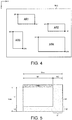
- FIG. 4 An exemplary setting of the error detection region is shown in Fig. 4 .
- first to fourth error detection regions AR1 to AR4 are set in an image IMG of a given frame.
- the size (width and height) of each error detection region is smaller than the size of the image IMG. That is, an error is not detected in the entire region of the image IMG, but is detected in a portion of the image IMG, namely the error detection regions AR1 to AR4.
- the error detection regions AR1 to AR4 are respectively designated by start points SP1 to SP4 and end points EP1 to EP4. Specifically, as a result of acquiring the coordinates of the start points SP1 to SP4 and the coordinates of the end points EP1 to EP4 as position information, the error detection regions AR1 to AR4 are designated.
- a coordinate x in a horizontal scan direction and a coordinate y in a vertical scan direction are defined using the coordinates of the upper left pixel of the image IMG as the origin, for example.
- the pixel having the smallest coordinate x and the smallest coordinate y is the start point and the pixel having the largest coordinate x and the largest coordinate y is the end point.
- the processing device 200 calculates CRC values for the respective error detection regions AR1 to AR4, and the CRC values are transmitted to the circuit device 100 as the expectation values. Also, the error detection unit 130 calculates CRC values for the respective error detection regions AR1 to AR4, and compares the calculated values and the respective expectation values.
- the number of error detection regions is not limited to four, and any number of two or more error detection regions can be set.
- the error detection regions AR1 to AR4 do not overlap each other, but there is no limit to this, and they may be partially overlapped regions.
- the position information that designates each error detection region is not limited to the start point and the end point, and may be any information with which the region can be determined.
- the position information may be the coordinates of the start point, the width (number of pixels in the horizontal scan direction), and the height (number of pixels in the vertical scan direction) of the error detection region.
- an error is detected not in the entire image, but in the error detection regions, which is a portion of the image. Accordingly, the amount of data used when the processing device 200 calculates the CRC values is reduced, and the processing load of the processing device 200 can be reduced. Also, as a result of setting a plurality of error detection regions, an error can be detected in a wider region of the image, and the occurrence of detection failures of an error can be reduced. If the error detection region is set to a particularly important region, effective error detection can be performed.
- the error detection regions in a given one frame are shown in Fig. 4 , but the setting of the error detection regions can be changed frame by frame. That is, in the present embodiment, the number, position, size, shape of the error detection regions can be variably set for each frame. In other words, in an i th frame image, an error is detected in an i th frame error detection region, in a j th frame image, an error is detected in a j th frame error detection region, and the positions of the error detection regions for the i th and j th frames are different.
- n is an integer of two or more
- i and j are integers of one or more and n or less
- i ⁇ j are integers of one or more and n or less.
- an error can be detected in the error detection region set at a different position in each frame, and as a result, an error can be detected in a wider range in the image. Also, since an error is detected in a region that is smaller than the entire image, the processing load of the processing device 200 can be reduced.
- the detecting of an error is to check whether or not the image data that the processing device 200 transmitted to the circuit device 100 matches the image data that the circuit device 100 has actually received (detection of a communication error).
- the frame image is an image (or an image to be displayed) that is displayed in one frame. For example, when the display in the display panel is updated at a rate of 30 fps (frames per second), the period of one frame is 1/30 seconds, and an image rendered in one frame is the frame image.
- the frame image here, is an image at a stage when the processing device 200 transmits to the circuit device 100. That is, the finally displayed frame image is not necessarily the same as the frame image on which the error detection is performed, because image processing may be performed therebetween.
- the circuit device 100 includes the interface unit 160 that receives image data and the error detection unit 130 that performs error detection.
- the interface unit 160 includes the interface (an RGB method, etc.) for image data and the interface (an 12C method or a three-wire or four-wire serial transmission method, etc.) for error signal and register value, but the interface unit 160 here is an interface for image data, in a narrow sense.
- the interface unit 160 receives image data including display image data and error detection data that includes at least position information regarding the error detection region, and the error detection unit 130 performs error detection on the display image data based on the display image data of the error detection region specified by the position information.
- error detection data can be included in the image data.
- the circuit device 100 of the present embodiment can receive the error detection data using the interface for receiving the display image data.
- Fig. 5 is a schematic diagram of an image region (including a display region and a non-display region) corresponding to the image data of the present embodiment.
- th1 in Fig. 5 indicates the number of pixels (size) of an effective image area (display region) in a horizontal direction
- tv1 indicates the number of pixels of the effective image area in a vertical direction.
- the area (total number of pixels) of the effective image area, that is, the size of an image to be displayed is th1 ⁇ tv1.
- the image data to be used for actual display is referred to as display image data.
- the display image data is data in the effective image area, and is data including th1 ⁇ tv1 ⁇ 24 bits in the above example.
- a horizontal flyback period is provided, which is a period from when one line of data in the horizontal direction is displayed until display of the next one line of data is started.
- A1 in Fig. 5 illustrates a region corresponding to the horizontal flyback period for the sake of convenience, and th2 represents the number of pixels is the region.
- a vertical flyback period is provided, which is a period from when an image of one frame is displayed until display of an image of the next frame is started.
- A2 in Fig. 5 illustrates a region corresponding to the vertical flyback period for the sake of convenience, and tv2 represents the number of pixels in the region.
- a region A3 determined by A1 and A2 is a non-display region that is not used for image display.
- the data in the effective image area is the display image data, and therefore it is not preferable that error detection data is included in the effective image area. This is because an image cannot be displayed in the effective image area if error detection data is written into the data thereof.
- the error detection data may be added to data in the non-display region.
- the non-display region corresponds to the flyback period, and therefore addition of data to the data in the non-display region does not interfere with the transmission and reception of display image data. Note that a case where adding error detection data to the data in the non-display region is difficult is conceivable depending on the communication standard.
- the interface unit 160 receives image data in which error detection data is added on a front side of the display image data, as shown by LINE0 in Fig. 5 . In this way, the error detection data can be appropriately received without interfering with the reception of display image data.
- data for a line in the horizontal direction can be included in LINE0.
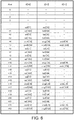
- Fig. 6 shows an example of a data format of LINE0.
- the error detection data includes expectation value information used for the error detection.
- the interface unit 160 receives image data including error detection data that includes position information regarding the error detection region and expectation value information used for the error detection.
- An example in which four error detection regions are set is envisioned in Fig. 6 , and the error detection information includes four pieces of position information and expectation value information.
- the position information includes coordinates of the start points SP1 to SP4 (coordinates of pixels corresponding to the start points) and coordinates of the end points EP1 to EP4 (coordinates of pixels corresponding to the end points), for example.
- the error detection unit 130 sets the rectangle regions whose diagonal lines are lines connecting the respective start points and end points as the error detection regions.
- the values of hs, vs, he, and ve need only represent information with which one pixel in the effective image area can be specified. For example, if the effective image area has a size of 1920 ⁇ 1080, 11-bit data may be used as values of the position information. Note that various modifications can be implemented with respect to the number of bits.
- the expectation value information is obtained by the processing device 200 on a transmission side, and the expectation value information for an i th frame error detection region, for example, is obtained by the processing device 200 from the display image data for the i th frame error detection region, of the display image data of the i th frame image.
- the expectation value information includes an expectation value crcr based on R data values of the pixels in the error detection region, and expectation value crcg based on G data values of the pixels in the error detection region, and an expectation value crcb based on B data of the pixels in the error detection region.
- crcr, crcg, and crcb are each 16-bit data, but various modifications can be implemented with respect to the number of bits as well.
- the expectation value information in the present embodiment may be the expectation value itself, but is not limited thereto, and may be information based on which the expectation value (alternatively, information corresponding to the expectation value) can be calculated.
- the region from an i th pixel to an i+6-th pixel, of LINE0 corresponds to the position information and the expectation value information regarding the first error detection region.
- a vertical coordinate value vs0 of the start point is stored using 11 bits out of 16 bits of R regions of the i and (i+1) th pixels.
- a horizontal coordinate value hs0 of the start point is stored using 11 bits out of 16 bits of G regions of the i and (i+1) th pixels
- a vertical coordinate value ve0 of the end point is stored using 11 bits of R regions of the i+2 and i+3-th pixels
- a horizontal coordinate value he0 of the end point is stored using 11 bits of G regions of the i+2 and i+3-th pixels.
- B regions in the i to i+3 pixels are not used.
- an expectation value crcr0 based on the R data is stored using 16 bits of R regions of the i+4 and i+5-th pixels.
- an expectation value crcg0 based on G data is stored using 16 bits of G regions of the i+4 and i+5-th pixels
- an expectation value crcb0 based on B data is stored using 16 bits of B regions of the i+4 and i+5-th pixels.
- i+6 to i+11 pixels correspond to the second error detection region
- i+12 to i+17 pixels correspond to the third error detection region
- i+18 to i+23 pixels correspond to the fourth error detection region.
- the error detection data needs only be in a format such that the circuit device 100 on the reception side can specify the position information and the expectation value information for each of the error detection regions, and the data format thereof is not limited to that shown in Fig. 6 .
- the order of the position information and the expectation value information regarding each of the error detection regions is not limited to the order shown in Fig. 6 .
- the image data includes second to n th pieces of error detection data (n is an integer of two or more), and i th (i is an integer that satisfies 2 ⁇ i ⁇ ) error detection amount data of the second to n th pieces of error detection data includes position information corresponding to an i th error detection region.
- the interface unit 160 receives i th to n th pieces of error detection data that respectively correspond to i th to n th error detection regions (n is an integer of two or more) and include pieces of position information regarding the respective error detection regions.
- a plurality of error detection regions can be appropriately set for each frame.
- a plurality of error detection regions need not be set for each frame, and a frame for which one error detection region is set may be included.
- a frame for which the error detection region is not set, and as a result, the error detection (and error determination) is to be skipped may be included.
- the circuit device 100 since the circuit device 100 can receive error detection data for each frame using the image data, the error detection region can be flexibly set.
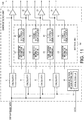
- the error detection unit 130 includes calculators 11 to 14 (calculation circuits) and comparators 21 to 24 (comparison circuits).
- the error determination information output unit 140 includes first determination units 81-1 to 81-4, second determination units 82-1 to 82-4, and third determination units 83-1 to 83-4. Note that, here, a case in which four calculators and the like are included will be described as an example, but the number of calculators and the like may be any number of two or more (the same number as the maximum number of settable error detection regions, for example). In the following, the units of the error detection unit 130 and the error determination information output unit 140 will be described in detail.
- Position information regarding the first error detection region of the error detection data and display image data are input to the calculator 11.
- the calculator 11 calculates a CRC value (calculated value) based on display image data, of the display image data, in the first error detection region specified by the position information.
- the calculator 11 calculates an error detection code of the image data.
- Various types of methods are widely known for the type and calculation method of the error detection code, and these can be widely applied in the present embodiment.
- the calculator 11 outputs the calculated CRC value to the comparator 21 and the first determination unit 81-1.
- Expectation value information regarding the first error detection region of the error detection data and the CRC value calculated by the calculator 11 are input to the comparator 21.
- the CRC expectation value transmitted from the processing device 200 and the CRC value calculated by each of the calculators 11 to 14 include the same number of bits, and are calculated using the same computation expression.
- the comparator 21 performs comparison processing to determine whether or not the calculated CRC value matches the expectation value. That is, the error detection unit 130 performs error detection based on the expectation value information.
- the comparator 21 outputs a signal representing the comparison result (comparison result signal) to the second determination unit 82-1 and the third determination unit 83-1.
- the calculators 12 to 14 and the comparators 22 to 24 similarly operate as the calculator 11 and the comparator 21, calculate CRC values of the corresponding error detection regions and perform comparison processing, and output the CRC values and the comparison result signals to the corresponding determination units of the error determination information output unit 140.
- the error detection unit 130 needs the error detection data (position information, expectation value information) and the display image data in order to perform error detection.
- the display image data for the entire image need not be acquired, and it is sufficient that the error detection unit 130 acquires display image data for an error detection region specified by the position information. That is, when display image data to be processed is received, sequential calculation (using pipeline processing) of the CRC value by the calculator 11 may be started. In this way, effective error detection can be performed.
- the error detection unit 130 performs error detection on the display image data based on the error detection data that is added on a front side of the display image data.
- “front side” means data received by the interface unit 160 at an earlier temporal timing.
- "front side” means an upper side in the image, and a left side in the same line.
- the error detection data is received first, and thereafter the display image data is received. Therefore, the error detection data for performing the error detection on the display image data can be included in the image data for the same frame.
- the error detection data may be added on a back side of the display image data.
- the error detection data included in the image data for a given frame is used for the error detection to be performed on the display image data for the next frame. That is, the display image data and the error detection data corresponding to the display image data are included in pieces of image data for different frames.
- the interface unit 160 receives the display data used for display in an electro-optical panel from the processing device 200 as the image data, and the error detection unit 130 detects an error that occurs when the image data is transferred. Also, the error detection code used for the error detection is that of a cyclic redundancy check (CRC).
- CRC cyclic redundancy check
- the error detection performed by the circuit device 100 according to the present embodiment is specifically processing for checking whether or not, when the display image data is received, the received display image data is the same as the display image data that has been transmitted.
- the error detection unit 130 performs processing for comparing the CRC value with the expectation value. That is, when the comparison result indicates a mismatch, a communication error has occurred in the display image data. Therefore, the error determination information output unit 140 may output an error signal (interrupt request signal) to the processing device 200 when the comparison result signal indicates a mismatch.
- an error signal interrupt request signal
- the frequency of occurrence of an error in communication is specified to some degree according to a communication standard, and a standard is conceivable in which the bit error rate is required to be less than or equal to 10 -9 .
- This is a probability that a data error will occur when one-bit data is transferred, and when the size of one frame image is th1 ⁇ tv1 and the data size of one pixel is 24 bits, the probability that an error will occur per one frame is th1 ⁇ tv ⁇ 24 ⁇ 10 -9 .
- the specific value depends on the image size, if the image includes 1920x1080 pixels, for example, it is possible that an error will occur once about every 20 frames.
- the interrupt request signal will be output 1.5 times per second if the frame rate is 30 fps, and three times per second if the frame rate is 60 fps. These values are excessively high as the frequency of occurrence of the interrupt processing, and it is possible that the processing device 200 will not operate smoothly.
- the output frequency of the interrupt request signal (frequency of occurrence of the interrupt processing) can be reduced, but it is not sufficient.
- error determination may further be performed based on the output from the error detection unit 130.
- the circuit device 100 includes the interface unit 160 that receives image data, the error detection unit 130 that performs error detection by calculating an error detection code for the image data, and the error determination information output unit 140 that outputs error determination information based on the error detection codes calculated for a plurality of frames.
- the error determination information can be output based on the error detection codes calculated for a plurality of frames.
- an error of higher importance compared with a single error occurrence, such as a case where the number of error detections based on the error detection codes is large or a case where errors occur successively can be determined. Therefore, occurrence of an interruption at a high frequency as described above can be suppressed.
- the error detection unit 130 performs error detection by calculating error detection codes in a plurality of error detection regions of the image data, and the error determination information output unit 140 outputs error determination information for each of the plurality of error detection regions. That is, the error determination information can be output for each error detection region. Therefore, the content of the error determination can be adjusted according to the error detection region.
- the settings for an important region are such that an error is easily determined so as to suppress the overlooking of an error.
- the settings for a less important region are such that an error is not easily determined so as to suppress excessive output of the interrupt request signal.
- the error determination information output unit 140 may include the first determination units 81 (81-1 to 81-4), the second determination units 82 (82-1 to 82-4), and the third determination units 83 (83-1 to 83-4), as shown in Fig. 7 .
- the configuration of each determination unit is not limited to the configuration described below, and various modifications can be implemented.
- Fig. 8 shows an exemplary configuration of the first determination unit 81-1. Although a description will be omitted below, the first determination units 81-2 to 81-4 in Fig. 8 may be similarly configured.
- the first determination unit 81-1 includes delay circuits DA1-1 and DA1-2, a comparator CP1, and a frame counter FC1.
- a CRC value from the calculator 11 is input to the delay circuit DA1-1, and the delay circuit DA1-1 delays the CRC value by a period of one frame.
- An output from the delay circuit DA1-1 is input to the delay circuit DA1-2, and the delay circuit DA1-2 further delays the output of the delay circuit DA1-1 by the period of one frame.
- the delay circuits DA1-1 and DA1-2 are each realized by a D flip-flop, for example.
- the comparator CP1 compares the output of the delay circuit DA1-1 with the output of the delay circuit DA1-2. In other words, the comparator CP1 determines whether or not the CRC value in a frame i matches the CRC value in a frame i+1, which is one frame after the frame i.
- the frame counter FC1 is a counter that performs count up or is reset based on the output of the comparator CP1.
- the signal denoted by "matched” in Fig. 8 is a signal that is "1" (high level, activated) when the CRC values in frames i and i+1 match and "0" (low level, deactivated) when the CRC values do not match.
- the signal "unmatched” is a signal that is activated when the CRC values in frames i and i+1 do not match, and is deactivated when the CRC values match.
- the error determination information output unit 140 outputs first error determination information as the error determination information based on the result of comparison between the error detection code at the i th frame and the error detection code at the (i+1) th frame by using the first determination unit 81-1 shown in Fig. 8 .
- the display image data may include, in many cases, a region in which the display content (pixel value) does not change.
- a warning lamp for notifying a user of an abnormality in the vehicle may be displayed in a portion of the display panel.
- the warning lamp displays a first color pattern (a pattern in which all the warning lamp display region is green, for example) when there is no abnormality, and displays a second color pattern (entire region is red, for example) when there is an abnormality. In this way, the user is clearly notified of whether or not an abnormality has occurred.
- the case where the warning lamp displays the second color pattern is a case where a serious abnormality has occurred to such a degree that the user is in danger, and therefore, most of the time, the warning lamp displays the first color pattern.
- the CRC value in the error detection region is constant in many cases.
- a region in which continuation of a similar display is envisioned is conceivable other than the warning lamp, and if a region is set as the error detection region, the CRC value is expected to be the same over a long period of time.
- the first determination unit 81-1 checks the value of the frame counter FC1 at predetermined time intervals. If a communication error has not occurred, the count value of the frame counter FC1 is a value that is determined by the elapsed time (number of passed frames). On the other hand, if a communication error has occurred, since the frame counter FC1 is reset at a timing corresponding to the frame in which the communication error has occurred, the count value is smaller than the value when an error has not occurred. The first determination unit 81-1 determines whether or not a communication error has occurred based on the magnitude of the count value of the counter, and outputs the determination result as the first error determination information.
- Fig. 9 shows an exemplary configuration of the second determination unit 82-1. Although the description will be omitted below, the second determination units 82-2 to 82-4 in Fig. 7 may be similarly configured.
- the second determination unit 82-1 is realized by an integration counter AC1.
- the integration counter AC1 is a counter whose terminal UP receives an input of the comparison result signal from the comparator 21 of the error detection unit 130 and that counts up based on the comparison result signal.
- the comparison result signal is a signal that is "1" (activated) when the CRC value does not match the expectation value, and is "0" (deactivated) when the CRC value matches the expectation value.
- the comparison result signal may be a signal that is activated when the CRC value matches the expectation value, and is deactivated when the CRC value does not match the expectation value.
- the second determination unit 82-1 includes an unshown inverter circuit (NOT circuit) for inverting the comparison result signal, and the inverted result may be input to the terminal UP of the integration counter AC1.
- the integration counter AC1 counts up when the comparison result signal is activated, that is, when the CRC value does not match the expectation value. With this, in the integration counter AC1, the number of times the CRC value does not match the expectation value (number of times a CRC error has occurred) can be integrated. Also, the integration counter AC1 in which a predetermined threshold value is set determines that an error has occurred when the number of times the CRC error has occurred exceeds the threshold value. When the number of times the CRC error has occurred is large, it is considered that the severity of the error is high. That is, as a result of using the integration counter AC1, whether or not a severe communication error has occurred can be determined.
- the error determination information output unit 140 outputs second error determination information as the error determination information, when the integrated value of the number of error detection times based on the error detection code has reached a given number of times by using the second determination unit 82-1 shown in Fig. 9 .
- the given number of times here, can be variously set, and in the example in Fig. 9 , one of four candidates, namely 31, 63, 127, 255 times, can be selected. For example, a relatively small value may be set to an important error detection region, and a relatively large value may be set to an error detection region that is less important. In this way, flexible error determination according to the degree of importance is possible.
- Fig. 10 shows an exemplary configuration of the third determination unit 83-1. Although the description will be omitted below, the third determination units 83-2 to 83-4 in Fig. 7 may be similarly configured.
- the third determination unit 83-1 includes first to fourth delay circuits (D flip-flops) DB1-1 to DB1-4, and an AND circuit AN1.
- the comparison result signal from the comparator 21 of the error detection unit 130 is input to the first delay circuit DB1-1.
- An output bit1 of the first delay circuit DB1-1 is input to the second delay circuit DB1-2.
- An output bit2 of the second delay circuit DB1-2 is input to the third delay circuit DB1-3.
- An output bit3 of the third delay circuit DB1-3 is input to the fourth delay circuit DB1-4.
- the outputs bit1 to bit3 and an output bit4 of the fourth delay circuit DB1-4 are input to the AND circuit AN1.
- a signal corresponding to the frame timing of the image data is input to the delay circuits DB1-1 to DB1-4 as a clock signal. That is, the delay circuits DB1-1 to DB1-4 are each a circuit that delays a comparison result signal by one frame, and the outputs bit1 to bit4 represent comparison result signals at four different frames (four successive frames, in a narrow sense).
- the AND circuit AN1 outputs a logical product of the outputs bit1 to bit4, and therefore the output of the AND circuit AN1 is activated when all of the outputs bit1 to bit4 are activated, that is, when the CRC value does not match the expectation value in each of the four successive frames. It is possible that a CRC error itself will occur several times per second, as described above, but it is not conceivable that a CRC error occurs in each of a plurality of successive frames in a normal state. Therefore, when a CRC error occurs in each of a plurality of successive frames, it can be determined that a serious communication error has occurred.
- the error determination information output unit 140 outputs third error determination information as the error determination information when an error is detected based on the error detection code in each of a successive given number of set frames by using the third determination unit 83-1 shown in Fig. 10 .
- the given number of set frames is four is shown in Fig. 10 , but there is no limitation thereto.
- an unshown another AND circuit may be added to the configuration shown in Fig. 10 . Specifically, a two-input AND circuit to which the outputs bit1 and bit2 are input and a three-input AND circuit to which outputs bit1 to bit3 are input may be added.
- the third determination unit 83-1 is set such that the output thereof can be selected from the output bit1 itself, a logical product of the outputs bit1 and bit2, a logical product of the outputs bit1 to bit3, and a logical product of the outputs bit1 to bit4.
- the above-described given number of set frames can be selected from 1 to 4, and flexible error determination according to the degree of importance is possible.
- a configuration in which five frames or more can be set as the number of set frames may be adopted. Note that, similarly to the second determination unit 82-1 described above, the number of set frames may be reduced as the importance of the error detection region increases.
- first to third determination units are provided to each of the plurality of error detection regions are illustrated in Fig. 7 , but there is no limitation thereto.
- a modification in which the first determination unit 81 is not provided, or the first determination unit 81 is provided as a constituent element but does not operate (deactivated) in a given error detection region can be implemented.
- the output of the error determination information in the present embodiment can be realized using various methods.
- the output of the error determination information may be an output of the interrupt request signal to the processing device 200.
- the output of the error determination information may be written into the register unit 150.
- the processing device 200 regularly reads a corresponding region of the register unit 150 so as to confirm the error occurrence status (polling).
- the error determination information output unit 140 outputs the first error determination information from the above-described first determination unit 81 by writing to the register unit 150, and outputs the second error determination information from the second determination unit 82 and the third error determination information from the third determination unit 83 by outputting the interrupt request signal.
- the error determination information output unit 140 outputs the interrupt request signal based on eight determination results in the second determination units 82-1 to 82-4 and the third determination units 83-1 to 83-4.
- the interrupt request signal may be output when an error is determined in any one of the second determination units 82-1 to 82-4 and the third determination units 83-1 to 83-4.
- the processing device 200 may stop transmission of image data to the circuit device 100, or the processing device 200 may instruct the circuit device 100 so as to perform specific display control (black display (entire screen is black) or display of a predetermined pattern, for example). Alternatively, the processing device 200 may stop operating the circuit device 100 or reset the circuit device 100.
- the operation of the processing device 200 may be changed according to the error detection region in which an error has been determined to have occurred, out of the plurality of error detection regions.
- the operation of the processing device 200 may be changed according to the error determination information that has been output, out of the plurality of pieces of error determination information (first to third error determination information, in the above-described example).
- the error detection region can be flexibly set, and there are cases where the importance or the like will be different region by region.
- the contents of determination processing of the respective pieces of error determination information are different to each other, and therefore the error occurrence situation is different according to the type of determination in which an error has been determined. Therefore, as a result of specifying the error detection region and the content of the error determination information, the processing device 200 can appropriately deal with the error according to the region and the content of determination.
- the circuit device 100 of the present embodiment further includes the control unit 110 that controls the operations of the circuit device, and the error determination information output unit 140 outputs a plurality of pieces of error determination information for which determination processing with respect to the error detection code is different to each other as the error determination information. Also, the control unit 110 of the circuit device 100 controls the operations based on at least one of the information that indicates the error detection region in which an error has been determined to have occurred, out of the plurality of error detection regions, and the information indicating which of the plurality of pieces of error determination information has been output.
- the circuit device 100 may execute operation control for handling the error.
- operation control may include stopping output of image data to an external unit (output from the display controller 400, which is the circuit device 100, to the display driver 300, for example), and specific display control such as displaying a black pattern, a specific pattern, or an image saved inside the circuit device 100.
- the method of the present embodiment can be applied to the circuit device 100 including the interface unit 160 that receives image data, a first error detection unit that performs error detection by calculating an error detection code of the image data in a first error detection region of the image data, and a second error detection unit that performs error detection by calculating an error detection code of the image data in a second error detection region of the image data.
- the first error detection unit corresponds to the calculator 11 and the comparator 21 in the error detection unit 130 shown in Fig. 7
- the second error detection unit corresponds to the calculator 12 and the comparator 22, for example.
- the circuit device 100 includes a first error determination information output unit that outputs error determination information based on an error detection code of the image data in a first frame and an error detection code of the image data in a second frame, which comes after the first frame, that have been output from the first error detection unit, and a second error determination information output unit that outputs error determination information based on an error detection code of the image data in a third frame and an error detection code of the image data in a fourth frame, which comes after the third frame, that have been output from the second error detection unit.
- the first error determination information output unit corresponds to the first determination unit 81-1, the second determination unit 82-1, and the third determination unit 83-1 in the error determination information output unit 140 in Fig. 7 .
- the second error determination information output unit corresponds to the first determination unit 81-2, the second determination unit 82-2, and the third determination unit 83-2, for example.
- a plurality of error detection regions can be set to an image, and error detection processing and processing for outputting error determination information can be performed for each error detection region. That is, according to the method of the present embodiment, error determination or the like using a plurality of frames can be independently performed for each error detection region (the error detection unit 130 independently outputs an output for each error detection region). For example, a region in which a warning lamp is displayed may be the first error detection region, and the other region may be the second error detection region. In this way, processing can be performed for each region according to the properties of an error detection region (degree of importance, in a narrow sense).
- error detection data is included in image data
- the interface unit 160 receives the error detection data using an interface for image data. In this way, error detection data can be easily received in each frame without interfering with the reception of display image data, and it is not necessary to write error detection data into the register unit 150 or the like.
- the method of receiving the error detection data is not limited thereto.
- the error detection data may be received using an interface that is different from the interface for image data.
- the error detection may be performed by writing the received error detection data into the register unit 150. A detailed description will be given below.
- the error detection unit 130 includes calculators 11 to 14, comparators 21 to 24, and an error detection region setting unit 30 (error region setting circuit).
- the calculators 11 to 14 and the comparators 21 to 24 are similarly configured to those in Fig. 7 .
- the register unit 150 includes first to fourth position information registers 51 to 54 and first to fourth expectation value registers 61 to 64. Note that the number of calculators and the like may be any number of two or more, similarly to the example shown in Fig. 7 .
- Pieces of position information regarding the first to fourth error detection regions are respectively written into the position information registers 51 to 54 from the processing device 200.
- CRC expectation values of the first to fourth error detection regions are respectively written into the expectation value registers 61 to 64 from the processing device 200.
- the position information and the expectation value information are written into the register unit 150 via an interface that is different from that for image data through 12C communication, three-wire or four-wire serial communication, or the like.
- the expectation value information may be written into the register unit 150 via the interface for image data.
- the calculators 11 to 14 read out the position information from the respective position information registers 51 to 54, and calculate CRC values of the respective first to fourth error detection regions from the image data (display image data).
- the comparators 21 to 24 respectively compare the CRC expectation values of the first to fourth error detection regions from the expectation value registers 61 to 64 and the CRC values of the first to fourth error detection regions from the calculators 11 to 14.
- the comparators 21 to 24 each output a signal "0" (low level, deactivated) when the expectation value matches the CRC value, as a comparison result signal, and output a signal "1" (high level, activated) when the expectation value does not match the CRC value, as the comparison result signal.
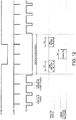
- a timing chart of the error detection processing is shown in Fig. 12 .
- a vertical synchronizing signal VSYNC, a horizontal synchronizing signal HSYNC, and a data enable signal DE are supplied to the control unit 110 (timing control unit) of the circuit device 100 from the processing device 200. Note that instead of these signals being directly supplied from the processing device 200, the control unit 110 may generate these signals based on a synchronization signal supplied from the processing device 200.
- the vertical synchronizing signal VSYNC is a signal for defining the vertical scan period (frame), and a period from a falling edge of the vertical synchronizing signal VSYNC to the next falling edge is one vertical scan period.
- Image data of one frame image is transmitted from the processing device 200 to the circuit device 100 in one vertical scan period.
- the horizontal synchronizing signal HSYNC is a signal for defining the horizontal scan period, and a period from a falling edge of the horizontal synchronizing signal HSYNC to the next falling edge is one horizontal scan period. In one horizontal scan period, image data of one horizontal scan line is transmitted from the processing device 200 to the circuit device 100.
- the data enable signal DE is activated (high level) in a portion (data valid period) of the horizontal scan period, and image data of a horizontal scan line is transmitted from the processing device 200 to the circuit device 100 in the activated period.
- a period between a data valid period and a data valid period is referred to as a horizontal flyback period, and image data is not transmitted in this period.
- a vertical flyback period is provided when switching of the vertical scan period is performed, and the data enable signal DE is deactivated (low level) in the vertical flyback period. Image data is not transmitted in this period.
- the vertical flyback period corresponds to four horizontal flyback periods, and the vertical synchronizing signal VSYNC is at a low level in two horizontal flyback periods thereof.
- Image data (display image data) of a frame image is transmitted in a period from when a vertical flyback period is ended until when the next vertical flyback period is started.
- the error detection processing is executed in the above-described vertical flyback period. That is, the processing device 200 writes CRC expectation values to the expectation value registers 61 to 64 in a first register access period TA1 after a vertical flyback period has started. These expectation values are expectation values that are obtained from the image data that was transmitted in a frame immediately before the vertical flyback period.
- the comparators 21 to 24 compare the CRC values calculated in the calculators 11 to 14 and the respective expectation values. Note that the calculators 11 to 14 calculate CRC values from the image data that was transmitted in a frame immediately before the vertical flyback period.
- This calculation processing is successively performed following the input of image data (that is, not limited to be performed in the vertical flyback period), and is ended before the error detection period TB1.
- the processing device 200 writes position information regarding the error detection regions to the position information registers 51 to 54. This position information is position information regarding the error detection region to be applied to image data that is to be transmitted in a frame immediately after the vertical flyback period.
- the error detection unit 130 may output the comparison result signals to the error determination information output unit 140 (error signal output unit), and the error determination information output unit 140 may output an error signal to the processing device 200 when a comparison result signal (detection signal) from the error detection unit 130 is activated. That is, the configuration of the error determination information output unit 140 may be simplified compared with that shown in Figs. 7 to 10 .
- the error detection unit 130 performs error detection on image data in each of the plurality of error detection regions, and outputs detection signals for the respective error detection regions (that is, outputs a plurality of detection signals). Also, the error signal output unit outputs an error signal when at least one of the plurality of detection signals is activated.
- the error detection region setting unit 30 sets (controls) which of the first to fourth error detection regions is to be the target of error detection.
- the error detection region setting unit 30 includes a frame counter 31 that counts the vertical synchronizing signal VSYNC, and selects an error detection region that is the target of error detection according to the count value of the frame counter 31.
- a case is considered in which error detection information regarding four error detection regions are stored in the register unit 150 using the first to fourth position information registers 51 to 54 and the first to fourth expectation value registers 61 to 64, as shown in Fig. 11 .
- four error detection regions AR1 to AR4 can be continuously set for each frame, as shown in Fig. 4 (hereinafter, referred to as "first method").
- first method modifications such as second to fourth methods described below can be implemented.
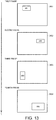
- FIG. 13 A diagram for describing the second method of error detection is shown in Fig. 13 .
- an error is detected in one error detection region with respect to one frame image.
- an error is detected in a first error detection region AR1 of a frame image IMG1 in a first frame
- an error is detected in a second error detection region AR2 of a frame image IMG2 in a second frame
- an error is detected in a third error detection region AR3 of a frame image IMG3 in a third frame
- an error is detected in a fourth error detection region AR4 of a frame image IMG4 in a fourth frame.
- Similar operations are repeated.
- the processing device 200 calculates a CRC value in the error detection region AR1 in the frame image IMG1, and writes the CRC value into the register unit 150 as the expectation value.
- the error detection unit 130 calculates a CRC value in the error detection region AR1 in the frame image IMG1, and compares the calculated value with the expectation value.
- the error signal output unit (error determination information output unit 140) outputs the interrupt request signal to the processing device 200 if the calculated value does not match the expectation value.
- similar error detection processing is performed on the second to fourth error detection regions AR2 to AR4. Note that the position information regarding each of the error detection regions AR1 to AR4 includes coordinates of start and end points, similarly to the first method.
- the error detection region used in each frame is controlled as follows, for example. That is, the pieces of position information regarding the respective error detection regions AR1 to AR4 are collectively written into the register unit 150, and which of the pieces of position information regarding the respective error detection regions is to be used for each frame is controlled based on the output of the frame counter.
- the processing device 200 writes a register value for designating which of the error detection regions is the target for each frame into the register unit 150, and the error detection unit 130 detects an error in the error detection region designated by the register value in each frame.
- the error detection unit 130 may detect an error in all of the error detection regions AR1 to AR4 in each frame, and the error signal output unit may validate (perform weighting) an error detection result with respect to the error detection region designated by the register value, and output the interrupt request signal based on only the validated error detection result.
- an error is detected not in the entire image, but in an error detection region, which is a portion of the entire image, and a different error detection region is set for each frame. Accordingly, the amount of data that the processing device 200 uses to calculate the CRC value is reduced, and the processing load of the processing device 200 can be reduced. Also, as a result of setting a different error detection region in each frame, an error can be detected in a wider region of the image, and the occurrence of detection failures of an error can be reduced.
- FIG. 14 A diagram for describing the third method of error detection is shown in Fig. 14 .
- an error is detected in a different number of error detection regions between the frame image in a first frame and the frame image in a second frame.
- an error is detected in a first error detection region AR1 of a frame image IMG1 in the first frame, and an error is detected in second to fourth error detection regions AR2 to AR4 of a frame image IMG2 in the second frame, for example.
- similar operations are repeated.
- the number of error detection regions may further be changed such as an error being detected in the first and second error detection regions AR1 and AR2 in the third frame, and an error being detected in the third and fourth error detection regions AR3 and AR4 in the fourth frame.
- the position information regarding each of the error detection regions AR1 to AR4 includes coordinates of start and end points, similarly to the first method. Also, the error detection region used in each frame is controlled by a method similar to the second method.
- the processing load of the processing device 200 can be reduced and an error can be detected in a wider region of the image, similarly to the second method.
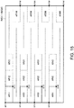
- FIG. 15 A diagram for describing the fourth method of error detection is shown in Fig. 15 .
- an image is divided into a plurality of regions, and the divided regions are sequentially selected for each frame, and an error is detected in the selected divided regions as the error detection region.
- Fig. 15 eight rows ⁇ (M/2) columns of divided regions are set, M (M is an integer of three or more, and M is an even number in the example in Fig. 15 ) divided regions are arranged in two rows.
- the divided regions in the first and second rows are denoted by AR11 to AR1M (first group of error detection regions), the divided regions in the third and fourth rows are denoted by AR21 to AR2M (second group of error detection regions), the divided regions in the fifth and sixth rows are denoted by AR31 to AR3M (third group of error detection regions), and the divided regions in the seventh and eighth rows are denoted by AR41 to AR4M (fourth group of error detection regions).
- the divided regions AR11, AR21, AR31, and AR41 are the error detection regions in a frame image IMG1 in a first frame, and the divided regions AR12, AR22, AR32, and AR42 are the error detection regions in a frame image IMG2 in a second image. This selection of the error detection regions is repeated until an M th frame, and the error detection regions that are the same as those in the first frame are assigned in an (M+1) th frame again.
- the error detection regions in each frame are controlled as follows, for example. That is, the processing device 200 writes position information regarding the divided regions (error detection regions) AR11, AR21, AR31, and AR41 into the register unit 150 in the first frame, and writes position information regarding the divided regions (error detection regions) AR12, AR22, AR32, and AR42 into the register unit 150 in the second frame. These operations are repeated until the M th frame so as to control the error detection regions in each frame.
- the position information includes coordinates of start and end points of each of the divided regions.
- the processing device 200 writes position information (coordinates of start and end points) of the first divided regions AR11, AR21, AR31, and AR41 in the first to fourth error detection regions and position information (coordinates of the end point) of the final divided regions AR1M, AR2M, AR3M, and AR4M to the register unit 150.
- the error detection unit 130 obtains the coordinates of start and end points of each of the divided regions from these pieces of position information. For example, in the case where the width of the divided region AR11 is 100 pixels, the coordinates obtained by shifting coordinates of a start point SP11 and an end point EP11 of the divided region AR11 by 100 in a horizontal scan direction are the coordinates of a start point and an end point of the divided region AR12.
- the error detection unit 130 shifts the divided region by one every time the vertical synchronizing signal is input, updates the register unit 150 with the position information regarding the divided region, and as a result, controls the error detection regions for each frame, for example.
- an error may be detected in all of the groups of the first to fourth error detection regions, or an error may be detected in a portion (any one group, two groups, or three groups) thereof.
- an error may be detected in all of the groups of the first to fourth error detection regions in the first to M th frames, and an error may be detected only in the fourth group of error detection regions in the next (M+1) th to 2M th frames.
- the processing device 200 performs control so as to indicate which of the groups are targeted by writing a register value indicating which of the groups are targeted to the register unit 150. For example, when an upper 3/4 of an image is black, and only the lower 1/4 of the image is displayed, the fourth group of error detection regions corresponding to the lower 1/4 of the image is targeted.
- Such control is possible because the processing device 200 is aware of the content of the image data. In an image whose image data indicates many continuous black areas, the CRC reliability (error detection rate) decreases, and therefore, by omitting calculation of the CRC value in such a region, the processing load of the processing device 200 can be reduced.
- the processing load of the processing device 200 can be reduced, similarly to the second and third methods. Also, as a result of sequentially selecting the divided regions for each frame, an error is detected in the entire image, and the occurrence of detection failures of an error can be further reduced.
- the processing device 200 calculates an expectation value for the error detection with respect to the entire image, and therefore the amount of data that is the target of calculation increases, and the processing load increases.
- the error detection region is a fixed region that is smaller than the entire image, although the processing load of the processing device 200 is reduced, an error can be detected only in a portion of the image.
- the circuit device 100 includes the error detection unit 130 that detects an error in image data, and the error signal output unit that outputs an error signal based on the error detection result.
- n is an integer of two or more
- i and j are each an integer of one or more and n or less, and satisfy an expression i ⁇ j.
- An i th frame error detection region is set to an i th frame image of first to n th frame images
- a j th frame error detection region is set to a position that is different from the i th frame error detection region, with respect to a j th frame image of the first to n th frame images.
- the error detection unit 130 detects an error based on the image data of the i th frame error detection region and the j th frame error detection region.
- the error signal output unit outputs an error signal based on the error detection result in the i th frame error detection region and the j th frame error detection region.
- an error is detected in the i th frame error detection region in the i th frame image, an error is detected in the j th frame error detection region in the j th frame image, and the positions of the i th and j th frame error detection regions are different. Accordingly, an error can be detected in an error detection region whose position is different for each frame, and an error can be detected in a wider region of the image. Also, since an error is detected in a region that is smaller than the entire image in one frame, the processing load of the processing device 200 can be reduced.
- the detecting of an error is to check whether or not the image data that the processing device 200 transmitted to the circuit device 100 matches the image data that the circuit device 100 has actually received (detection of a communication error).
- the error signal is a signal related to the result of an error detection, and is a signal indicating whether or not an error has been detected in image data, a signal for requesting the processing device 200 to perform some operations according to the error detection result, or the like, for example.
- a frame image is an image that is displayed (or an image to be displayed) in one frame. For example, when the display in the display panel is updated at a rate of 30 fps (frames per second), the period of one frame is 1/30 seconds, and an image rendered in one frame is the frame image.
- the frame image here, is an image at a stage when the processing device 200 is transmitting to the circuit device 100. That is, the finally displayed frame image is not necessarily the same as the frame image on which the error detection is performed, because image processing may be performed therebetween.
- n 4.
- an i th frame error detection region is a region AR1
- a j th frame error detection region is a region AR2.
- These error detection regions AR1 and AR2 are located at different positions.
- the position is indicated by the start point and end point of the region. Note that the indication of the position is not limited thereto, and the position may be indicated by only a start point or by a center point of the region (point where two diagonal lines intersect).
- the i th frame error detection region is a region AR1
- the j th frame error detection region includes regions AR2 to AR4.
- the i th and j th frame error detection regions may each be constituted by a plurality of regions.
- the position of the region is indicated by positions (start point and end point, for example) of each of the plurality of regions, and at least one of the plurality of regions needs only be located at different position.
- all regions AR2 to AR4 of the j th frame error detection region are located at positions that are different from that of the i th frame error detection region AR1.
- the j th frame error detection region may include the regions AR1 and AR2, for example. In this case, the region AR2 is located at a position different from the i th frame error detection region AR1.
- n M.
- the i th frame error detection region includes regions AR11 to AR41
- the j th frame error detection region includes regions AR12 to AR42.
- the circuit device 100 includes the register unit 150 for storing the position information regarding each of the i th frame error detection region and the j th frame error detection region.
- the i th frame error detection region and the j th frame error detection region are set based on the respective pieces of position information stored in the register unit 150.
- the position information includes coordinates of the start points SP1 to SP4 (coordinates of pixels corresponding to the start points) and coordinates of the end points EP1 to EP4 (coordinates of pixels corresponding to the end points), for example.
- the error detection unit 130 sets the rectangle regions whose diagonal lines are lines connecting the respective start points and end points as the error detection regions.
- error detection regions in which an error is to be detected can be set. Also, as a result of pieces of position information that are different from each other being written into the register unit 150 as the respective pieces of position information regarding the i th and j th frame error detection regions, i th and j th frame error detection regions that are located at different positions can be set.
- the register unit 150 stores expectation value information for error detection along with the position information regarding each of the i th and j th frame error detection regions.
- the error detection unit 130 performs the error detection based on the expectation value information.
- the expectation value information is obtained by the processing device 200 on the transmission side, and the expectation value information for the i th frame error detection region is obtained by the processing device 200 from the display data for the i th frame error detection region of the display data of the i th frame image, for example.
- an error can be detected with respect to the i th and j th frame error detection regions.
- the circuit device 100 includes the interface unit 160.
- the external processing device 200 sets the position information and expectation value information to the register unit 150 via the interface unit 160.
- the position information and the expectation value information are written into the register unit 150 via an interface that is different from that for image data through 12C communication, three-wire or four-wire serial communication, or the like.
- the expectation value information may be written into the register unit 150 via the interface for image data.
- the expectation value information is transmitted in a period in which image data is not transmitted (later-described flyback period, for example).
- the image data of one pixel includes 24 bits (8 bits for each of R, G, and B data)
- the expectation value information is a 16-bit CRC value
- a 16-bit CRC value is embedded in 24-bit data having the same format as the image data, and the 24-bit data is transmitted.
- the CRC value is assigned to the 16 bits including 8 bits for R data and 8 bits for G data, out of the 8 bits for each of R, G, and B data, and the CRC value is transmitted by the processing device 200.
- the interface unit 160 extracts the 16 bits including 8 bits for R data and 8 bits for G data out of the received 24 bits, and writes the extracted 16 bits to the register unit 150 as the expectation value information.
- timing control performed by the control unit 110 (timing control unit).
- the external processing device 200 sets the position information and expectation value information to the register unit 150 via the interface unit 160, and as a result, the error detection region can be set based on the position information, and an error can be detected in the error detection region based on the expectation value information.
- the expectation value information and position information received in a flyback period of image data are set to the register unit 150.
- the flyback period is a period in which image data is not transmitted, and is a vertical flyback period, for example.
- the vertical flyback period is a period (period combining horizontal scan periods in each of which a data valid period does not exist) between a period in which image data of a frame image is transmitted (period combining horizontal scan periods in each of which a data valid period exists) and a period in which image data of the next frame image is transmitted.
- the frame image with respect to which the processing device 200 has obtained the expectation value information needs to match the frame image on which the circuit device 100 performs error detection.
- the expectation value information is the expectation value information regarding the frame image received before the flyback period.
- the position information regarding the error detection region needs to be obtained prior to performing the error detection.
- the position information is the position information regarding the error detection region in the frame image to be received after the flyback period.
- a plurality of error detection regions are set as each of the i th and j th frame error detection regions.
- the third method in Fig. 14 three error detection regions AR2 to AR4 are set as the error detection region for the second frame.
- the fourth method in Fig. 15 four divided regions (AR11 to AR41, for example) are set as the error detection region for each frame.
- the i th and j th frame error detection regions may be set such that the number (variable number) of regions set in the i th frame error detection region is different from the number of regions set in the j th frame error detection region.
- one error detection region AR1 is set as the first frame error detection region, and the three error detection regions AR2 to AR4 are set as the second frame error detection region.
- a plurality of error detection regions are set as each of the error detection regions, or a different number of error detection regions are set as each of the error detection regions. Accordingly, flexible setting of the error detection region such as setting an appropriate error detection region according to the content of a display image is made possible. For example, if only in a portion of an image in one frame is displayed, one error detection region is set to the portion in the frame, and if a wide range of an image in another frame that is different from the one frame is displayed, a plurality of error detection regions can be set inside the range in the frame.
- the error detection unit 130 includes the error detection region setting unit 30.
- the error detection region setting unit 30 sets the regions in which an error is to be detected as each of the i th and j th frame error detection regions from a plurality of error detection regions based on the count value of the frame counter 31.
- position information regarding each of a plurality of error detection regions is set in the register unit 150, and the error detection region setting unit 30 performs control so as to select an error detection region to be the target of error detection (the error detection region with respect to which an error detection result is to be output) based on the count value.
- This control corresponds to setting the error detection region based on the count value.
- an error detection region to be the target of error detection in each frame is set, out of the plurality of error detection regions. Accordingly, control such as setting a plurality of error detection regions as each of the i th and j th frame error detection regions, and setting a different number of error detection regions as each of the i th and j th frame error detection regions can be performed.
- the error detection region setting unit 30 sets the error detection region such that a k th frame error detection region in a k th frame image, out of first to n th frame images, and a (k+1) th frame error detection region in a (k+1) th frame image are adjacent to each other, where k is an integer of one or more and n or less.
- the k th frame error detection region includes the regions AR11 to AR41
- the (k+1) th frame error detection region includes the regions AR12 to AR42.
- the regions AR12, AR22, AR32, and AR42 are respectively adjacent to the regions AR11, AR21, AR31, and AR41.
- regions being adjacent to each other means that one side of one region is adjacent to one side of the other region (there is no pixel therebetween, for example).
- the error detection regions are sequentially shifted to the respective adjacent regions for each frame. Accordingly, error detection can be performed on the entire image without a gap, in a period of a plurality of frames, and the accuracy of the error detection can be improved.
- the count value of the frame counter 31 is assumed to take values 0 to 15 (returning to 0 after 15), and the count values 0 to 15 are assumed to be associated with first to sixteenth frames, respectively.
- all the first to fourth error detection regions AR1 to AR4 are targeted regardless of the count value of the frame counter 31, and the error detection region setting unit 30 causes all the calculators 11 to 14 to calculate CRC values.
- the first error detection region AR1 is targeted when the count value of the frame counter 31 is 0, 4, 8, or 12, and second to fourth error detection regions AR2 to AF4 are not targeted. That is, the error detection region setting unit 30 causes the calculator 11 to calculate a CRC value, and disables operations of the calculators 12 to 14.
- the comparators 22 to 24 associated with the disabled calculators 12 to 14 each output "0" (deactivated). In this case, the processing device 200 writes register values only into the first position information register 51 and the first expectation value register 61.
- the second error detection region AR2 when the count value is 1, 5, 9, or 13, the second error detection region AR2 is targeted, when the count value is 2, 6, 10, and 14, the third error detection region AR3 is targeted, and when the count value is 3, 7, 11, and 15, the fourth error detection region AR4 is targeted.
- the processing device 200 writes register values to the first to fourth position information registers 51 to 54 and the first to fourth expectation value registers 61 to 64 in every frame. Also, regardless of the count value, the calculators 11 to 14 calculate respective CRC values, and the comparators 21 to 24 respectively compare the expectation values with the CRC values.
- the error detection region setting unit 30 causes the comparator 21 to perform weighting such that the comparison result of the comparator 21 is multiplied by 1, and causes the comparators 22 to 24 to perform weighting such that the comparison results of the comparators 22 to 24 are multiplied by 0. With this, the comparator 21 outputs the comparison result, and the comparators 22 to 24 output "0".
- the first error detection region AR1 when the count value of the frame counter 31 is 0, 2, 4, 6, 8, 10, 12, or 14, the first error detection region AR1 is targeted, and when the count value of the frame counter 31 is 1, 3, 5, 7, 9, 11, 13, or 15, the second to fourth error detection regions AR2 to AR4 are targeted.
- the error detection region setting unit 30 controls the calculators 11 to 14 and the comparators 21 to 24, similarly to the second method.
- a modified example is similarly configured.
- the processing device 200 writes position information regarding the error detection regions AR11 to AR41 to the first to fourth position information registers 51 to 54, and writes CRC expectation values of the error detection regions AR11 to AR41 to the first to fourth expectation value registers 61 to 64.
- the processing device 200 writes position information regarding the error detection regions AR12 to AR42 to the first to fourth position information registers 51 to 54, and writes CRC expectation values of the error detection regions AR12 to AR42 to the first to fourth expectation value registers 61 to 64.
- the regions are similarly shifted.
- the error detection region setting unit 30 causes the calculators 11 to 14 to calculate CRC values, and causes the comparators 21 to 24 to output comparison results, regardless of the count value of the frame counter 31.
- the error detection region setting unit 30 enables one of the calculators 11 to 14, and disables the others. For example, the calculators 11 to 13 are disabled, and the calculator 14 is enabled. In this case, only the fourth group of error detection regions AR41 to AR4M are the target of error detection. Note that, similarly to the modified example described in the second method, similar operations may be realized by weighting performed in the comparators 21 to 24. That is, the calculators 11 to 14 may be caused to calculate CRC values, the comparators 21 to 23 may be caused to multiply comparison results by 0, and the comparator 24 may be caused to multiply a comparison result by 1.
- the operations of the error detection region setting unit 30 described above can be realized by register setting, for example.
- the processing device 200 writes register values indicating which of the calculators 11 to 14 is enabled (or weighting performed in the comparators 21 to 24) at each count value, that is, an enabled calculator of the calculators 11 to 14 is associated with the count value of the frame counter 31, into the register unit 150, and the error detection region setting unit 30 operates referring to the register values.
- the processing device 200 writes mode setting values for switching between the first to fourth methods into the register unit 150 as the register value, and the error detection region setting unit 30 operates referring to the register values. In this case, which of the calculators 11 to 14 is enabled at each count value (or weighting performed in the comparators 21 to 24) is autonomously controlled by the error detection region setting unit 30.
- Fig. 16 shows a second detailed exemplary configuration of the register unit 150.
- the register unit 150 further includes first to fourth calculated value registers 71 to 74.
- CRC values (CRC calculated values) calculated by the calculators 11 to 14 are stored in the first to fourth calculated value registers 71 to 74.
- the processing device 200 can read out the CRC values from the first to fourth calculated value registers 71 to 74 via the interface unit 160.
- the processing device 200 can recognize a communication error of the image data, but cannot recognize the error detection region in which the error has occurred.
- the processing device 200 can recognize the error detection region in which the error has occurred by referring to the calculated value registers 71 to 74.
- the processing device 200 upon receiving an error signal (interrupt request signal), determines the error detection region in which the error has occurred by reading out the CRC values from the calculated value registers 71 to 74, and comparing the CRC values with the respective expectation values. For example, the processing device 200 can perform processing according to the region in which the error has occurred such as causing the circuit device 100 to re-transmit the image data in an area in which the error has occurred for re-rendering.
- Electro-optical device Electronic apparatus, and mobile body
- the method of the present embodiment can be applied to various devices including the above-described circuit device 100.
- the method of the present embodiment can be applied to an electro-optical device including the circuit device 100 and an electro-optical panel (display panel).
- the method of the present embodiment can be applied to an electronic apparatus and a mobile body including the circuit device 100.
- the electro-optical device includes the circuit device 100 (display controller), a display panel 360, and a display driver 300 that drives the display panel 360 under the control of the circuit device 100.
- the display panel 360 is constituted by a glass substrate and a pixel array (liquid crystal cell array) formed on the glass substrate, for example.
- the pixel array includes pixels, data lines, and scan lines.
- the display driver 300 is mounted on the glass substrate, and the display driver 300 and the pixel array are connected by an interconnect group that is formed by transparent electrodes (ITO: Indium Tin Oxide).
- the circuit device 100 is mounted on a circuit board that is different from the glass substrate, and the circuit board and the glass substrate are connected by a flexible board or the like. Note that the electro-optical device is not limited to this configuration.
- the display driver 300 and the circuit device 100 may be mounted on a circuit board, and the circuit board and the display panel 360 may be connected by a flexible board or the like.
- FIG. 18 An exemplary configuration of an electronic apparatus including the circuit device 100 of the present embodiment is shown in Fig. 18 .
- Various electronic apparatuses on which display devices are mounted such as an in-vehicle display device (such as meter panel, for example), a display, a projector, a television device, an information processing device (computer), a mobile information terminal, a car navigation system, a mobile gate terminal, and a DLP (Digital Light Processing) device, can be envisioned as the electronic apparatus of the present embodiment.
- the electronic apparatus includes a CPU 310 (processing device), the circuit device 100 (display controller), the display driver 300, the display panel 360, a storage unit 320 (memory), an operation unit 330 (operation device), and a communication unit 340 (communication circuit, communication device).
- a CPU 310 processing device
- the circuit device 100 display controller
- the display driver 300 the display panel 360
- a storage unit 320 memory
- an operation unit 330 operation device
- a communication unit 340 communication circuit, communication device
- the operation unit 330 is a user interface for receiving various operations made by a user.
- the operation unit 330 is constituted by a button, a mouse, a keyboard, a touch panel attached to the display panel 360, and the like.
- the communication unit 340 is a data interface for communicating (transmission, reception) image data and control data.
- the communication unit 340 is a wired communication interface such as a USB or a wireless communication interface such as a wireless LAN, for example.
- the storage unit 320 stores image data input from the communication unit 340.
- the storage unit 320 functions as a working memory of the CPU 310.
- the CPU 310 performs processing to control the units of the electronic apparatus, and various types of data processing.
- the circuit device 100 performs processing to control the display driver 300.
- the circuit device 100 converts the format of image data transferred from the communication unit 340 or the storage unit 320 via the CPU 310 to a format that can be accepted by the display driver 300, and outputs the converted image data to the display driver 300.
- the display driver 300 drives the display panel 360 based on the image data that has been transferred from the circuit device 100.
- FIG. 19 An exemplary configuration of a mobile body that includes the circuit device 100 of the present embodiment is shown in Fig. 19 .
- Various types of mobile bodies such as a car, an airplane, a motorcycle, a ship, and a robot (mobile robot, walking robot) can be envisioned as a mobile body of the present embodiment, for example.
- the mobile body is an apparatus or device that includes a drive mechanism such as an engine or a motor, steering mechanisms such as a steering wheel or a rudder, and various electronic apparatus, for example, and moves on the ground, in the air, and on the sea.
- Fig. 19 schematically illustrates an automobile 206 serving as a specific example of the mobile body.
- a display device 350 electronic-optical device
- the ECU 510 generates an image (image data) that shows pieces of information such as speed, remaining fuel amount, travel distance, and settings of various types of devices (air conditioner, for example) to a user, and transmits the image to the display device 350 so as to cause the display panel 360 to display the image.
- the invention is industrially applicable as a circuit device, an electro-optical device, an electronic apparatus, a mobile body, and an error detection method.
Landscapes
- Engineering & Computer Science (AREA)
- Signal Processing (AREA)
- Physics & Mathematics (AREA)
- Theoretical Computer Science (AREA)
- Computer Hardware Design (AREA)
- General Physics & Mathematics (AREA)
- Multimedia (AREA)
- Computer Networks & Wireless Communication (AREA)
- Probability & Statistics with Applications (AREA)
- Control Of Indicators Other Than Cathode Ray Tubes (AREA)
- Controls And Circuits For Display Device (AREA)
Abstract
Description
- The present invention relates to circuit devices, electro-optical devices, electronic apparatuses, mobile bodies, error detection methods, and the like.
- When display control is performed on a display device (liquid-crystal display device, for example), a processing device such as a CPU transmits image data and a control signal to a display controller, the display controller performs image processing and generates a timing signal, and a driver operates based on the image data subjected to image processing and the timing signal. The image data is transmitted from the processing device to the display controller using an LVDS (Low Voltage Differential Signal) method or a digital RGB method, for example. In any case, an error may occur in the image data due to a communication error or the like. For example, in
Patent Documents 1 to 3, a method is disclosed in which a display controller performs error detection on image data received from a processing device, using CRC (Cyclic Redundancy Check). -
- Patent Document 1:
JP-A-2012-35677 - Patent Document 2:
JP-A-2007-101691 - Patent Document 3:
JP-A-2007-72394 - In such error detection, a processing device obtains expectation value information (CRC expectation value, for example) for error detection from image data to be transmitted to a display controller, and the display controller obtains a calculated value (CRC value, for example) for error detection from the image data received from the processing device, and performs the error detection by comparing the expectation value information with the calculated value. Therefore, a processing load for obtaining the expectation value information for error detection is incurred in the processing device. For example, when all pieces of image data for one frame image is subjected to error detection, the amount of data used for calculating the expectation value information becomes excessive, and the processing load increases. Although a method is conceivable in which the region subjected to the error detection is reduced (only a portion of an image is subjected to error detection), an error cannot be detected in the image in a region other than the region subjected to error detection.
- According to some aspects of the invention, a circuit device in which a processing load of a processing device when error detection is performed on image data can be reduced, an electro-optical device, an electronic apparatus, a mobile body, an error detection method, and the like can be provided.
- One aspect of the invention relates to a circuit device including: an interface unit that receives image data; and an error detection unit that performs error detection. The interface unit receives the image data including display image data and error detection data that includes at least position information regarding an error detection region, and the error detection unit performs the error detection on the display image data based on the display image data of the error detection region that is specified by the position information.
- According to one aspect of the invention, both the display image data and the error detection data are received by the interface unit that receives image data. Also, the error detection data includes position information regarding the error detection region. In this way, the error detection data can be received by an interface similar to the interface that receives image data. Accordingly, the error detection region can be flexibly set for each frame, and a reduction in the processing load in error detection and the like can be realized.
- Also, in one aspect of the invention, the error detection data further includes expectation value information that is used in the error detection, and the error detection unit may perform the error detection based on the expectation value information.
- In this way, appropriate error detection can be performed using error detection information including the expectation value information.
- Also, in one aspect of the invention, the image data may include second to nth pieces of error detection data (n is an integer of two or more), and ith (i is an integer that satisfies 2≤i≤) error detection amount data of the second to nth pieces of error detection data may include the position information corresponding to an ith error detection region.
- In this way, a plurality of error detection regions being flexibly set with respect to one image (one frame image) and the like becomes possible.
- Also, in one aspect of the invention, the error detection unit may perform the error detection based on the ith error detection data in the ith error detection region.
- In this way, an error can be detected in each of a set plurality of error detection regions.
- Also, in one aspect of the invention, the error detection unit may perform the error detection on the display image data based on the error detection data that is added on a front side of the display image data.
- In this way, display image data and error detection data used to perform error detection on the display image data can be included in image data of the same frame and the like, and therefore effective data communication and error detection are enabled.
- Also, in one aspect of the invention, the circuit device further includes an error determination information output unit. The error detection unit may perform the error detection by computing error detection codes in a plurality of error detection regions of the image data, and the error determination information output unit may output error determination information with respect to the plurality of error detection regions based on the error detection code in the plurality of frames.
- In this way, error determination based on time series error detection codes is performed, and therefore flexible error determination can be performed according to a situation.
- Also, in one aspect of the invention, the error determination information output unit may output first error determination information as the error determination information based on a result of comparison between the error detection code in a jth frame (j is an integer of one or more) and the error detection code in a (j+1)th frame.
- In this way, error determination information can be output based on whether or not the error detection codes in different frames match.
- Also, in one aspect of the invention, the error determination information output unit may output second error determination information as the error determination information when an integrated value of the number of error detection times based on the error detection code reaches a given number of times.
- In this way, error determination information can be output based on an integrated value of the error detection number of times.
- Also, in one aspect of the invention, the error determination information output unit may output third error determination information as the error determination information when an error is detected based on the error detection code in each of a successive given number of set frames.
- In this way, error determination information can be output based on the number of successive error detections.
- Also, in one aspect of the invention, the circuit device further includes a control unit that performs operation control on the circuit device. The error determination information output unit may output a plurality of pieces of error determination information whose determination processing with respect to the error detection code is different to each other as the error determination information, and the control unit may perform the operation control based on at least one of the error detection regions in which an error has been determined, out of the plurality of error detection regions, and the error determination information that has been output, out of the plurality of pieces of error determination information.
- In this way, appropriate operations can be executed according to the error detection region in which an error has been determined, or the error determination information that has been output.
- Also, in one aspect of the invention, a jth frame error detection region and a kth frame error detection region may be set such that the number of regions in the jth frame error detection region and the number of regions in the kth frame error detection region are different.
- According to one aspect of the invention, a plurality of error detection regions are set as the error detection region for each frame, or a different number of error detection regions are set as the error detection region for each frame. Accordingly, flexible setting of error detection regions such as setting appropriate error detection regions according to the content of a display image becomes possible.
- Also, another aspect of the invention relates to an electro-optical device including the circuit device according to any of the above descriptions; and an electro-optical panel.
- Also, another aspect of the invention relates to an electronic apparatus including the circuit device according to any of the above descriptions.
- Also, another aspect of the invention relates to a mobile body including the circuit device according to any of the above descriptions.
- Also, another aspect of the invention relates to an error detection method including: receiving image data including display image data and error detection data that includes at least position information regarding an error detection region; and performing error detection on the display image data based on the display image data of the error detection region that is specified by the position information.
-
-
Fig. 1 shows an exemplary configuration of a circuit device. -
Fig. 2 shows another exemplary configuration of the circuit device. -
Fig. 3 shows another exemplary configuration of the circuit device. -
Fig. 4 shows an exemplary setting of an error detection region. -
Fig. 5 is a schematic diagram for describing an image region. -
Fig. 6 shows an exemplary data structure when error detection data is included in image data. -
Fig. 7 shows a detailed exemplary configuration of an error detection unit and an error determination information output unit. -
Fig. 8 shows an exemplary configuration of a first determination unit. -
Fig. 9 shows an exemplary configuration of a second determination unit. -
Fig. 10 shows an exemplary configuration of a third determination unit. -
Fig. 11 shows another exemplary configuration of the error detection unit and a register unit. -
Fig. 12 is a timing chart of error detection processing. -
Fig. 13 shows an exemplary setting of the error detection region. -
Fig. 14 shows an exemplary setting of the error detection region. -
Fig. 15 shows an exemplary setting of the error detection region. -
Fig. 16 shows another exemplary configuration of the register unit. -
Fig. 17 shows an exemplary configuration of an electro-optical device. -
Fig. 18 shows an exemplary configuration of an electronic apparatus. -
Fig. 19 shows an exemplary configuration of a mobile body. - The following is a detailed description of preferred embodiments of the invention. Note that the embodiments described below are not intended to unduly limit the content of the invention recited in the claims, and all of the configurations described in the embodiments are not necessarily essential as solutions provided by the invention.
- An exemplary configuration of a circuit device 100 (display controller 400) of the present embodiment is shown in
Fig. 1 . Thecircuit device 100 includes a control unit 110 (control circuit), an image processing unit 120 (image processing circuit), an error detection unit 130 (error detection circuit), an error determination information output unit 140 (error determination information output circuit), a register unit 150 (register), andinterface units 160 and 170 (interface circuits). Thecircuit device 100 is realized by an integrated circuit device (IC), for example. - The
interface unit 160 performs communication between aprocessing device 200 and thecircuit device 100. For example, theinterface unit 160 receives image data transmitted from theprocessing device 200 to theimage processing unit 120, and receives timing control signals (such as a clock signal, vertical synchronizing signal, horizontal synchronizing signal, data enable signal, for example) that are transmitted from theprocessing device 200 to thecontrol unit 110. Also, as will be described later usingFig. 11 and the like, writing to theregister unit 150 may be performed by theprocessing device 200. In this case, theinterface unit 160 receives a register value to be written to theregister unit 150, from theprocessing device 200. Alternatively, theinterface unit 160 transmits error determination information (error signal, error detection signal) that the error determinationinformation output unit 140 outputs to theprocessing device 200, and transmits a register value that theprocessing device 200 reads out from theregister unit 150. - An LVDS (Low Voltage Differential Signal) method, an RGB serial method, and a transmission method of the display port standard can be adopted as the communication method of the image data and the timing control signal. An 12C method, a three-wire or four-wire serial transmission method, or the like can be adopted as the communication method of the error signal and the register value. The
interface unit 160 is constituted by an input/output buffer circuit and a control circuit (such as PLL circuit in the LVDS method, for example) so as to realize such a communication method. - Note that, when the
circuit device 100 is mounted on an automobile or the like, for example, theprocessing device 200 is an ECU (Electronic Control Unit). Alternatively, when thecircuit device 100 is mounted on an electronic apparatus such as an information communication terminal, theprocessing device 200 is a processor such as a CPU (Central Processing Unit) or a microprocessor. - The
processing device 200 transmits error detection data including position information regarding the error detection region and a CRC expectation value (expectation value information for error detection) with respect to the error detection region to the circuit device 100 (display controller 400). Specifically, as will be described usingFigs. 5 and6 , theprocessing device 200 transmits display image data to be used for actual display and error detection data as the image data. In other words, theprocessing device 200 transmits the error detection data via an interface (such as above-described LVDS method or RGB serial method) for transmitting image data, of theinterface unit 160. Alternatively, as will be described later usingFig. 11 and the like, theprocessing device 200 may also write the error detection data into theregister unit 150 via a register value interface (such as 12C method). - The
control unit 110 controls the units of thecircuit device 100. Specifically, thecontrol unit 110 may perform timing control, and controls the units of thecircuit device 100 and generates timing control signals (such as a clock signal, vertical synchronizing signal, horizontal synchronizing signal, and data enable signal) to be transmitted to adisplay driver 300, based on a timing control signal from theprocessing device 200. - The
image processing unit 120 performs various types of image processing (such as tone correction, for example) and data formatting processing (processing for generating transmission data that conforms to the data reception method of the driver 300) on the image data (display data) from theprocessing device 200. - The
error detection unit 130 performs error detection processing on the image data from theprocessing device 200. In the following, a case where theerror detection unit 130 performs the error detection processing using a CRC (Cyclic Redundancy Check) will be described, as an example. Note that the method of error detection is not limited to the CRC, and a method such as checksum can be adopted, for example. A detailed exemplary configuration of theerror detection unit 130 will be described later. - The error determination
information output unit 140 outputs error determination information based on the output (a CRC value or a comparison result signal indicating a result of comparison between a CRC value and an expectation value) of theerror detection unit 130. Outputting error determination information is to output error determination information (error signal) to theprocessing device 200, or to write the error determination information into theregister unit 150, for example. The error signal here may be an interrupt request signal (IRQ: Interrupt ReQuest), for example. Alternatively, the error signal may be a signal (that is activated when an error has been determined) simply indicating that an error has been determined. - As will be described later in
Fig. 4 , a plurality of error detection regions are set in an image, in the present embodiment. Theerror detection unit 130 performs error detection on the image data for each error detection region, and outputs a CRC value and a comparison result signal for each error detection region. Also, the error determinationinformation output unit 140 performs error determination for the error detection regions based on the respective CRC values and the comparison result signals, and outputs respective pieces of error determination information. A detailed exemplary configuration of the error determinationinformation output unit 140 will be described later. - The
interface unit 170 performs communication between thecircuit device 100 and thedisplay driver 300. For example, theinterface unit 170 transmits image data output by theimage processing unit 120 to thedisplay driver 300, and transmits the timing control signals output by thecontrol unit 110 to thedisplay driver 300. Also, theinterface unit 170 may transmit a setting signal (mode setting signal, for example) for controlling the operation of thedisplay driver 300 to thedisplay driver 300. A similar communication method as that of theinterface unit 160 can be adopted as the communication method. - Note that the
display driver 300 is a circuit device that drives a display panel (electro-optical panel such as a liquid-crystal display panel or an electrophoretic display panel, for example). Thedisplay driver 300 is constituted by a data driver that drives a data line of the display panel, a scan driver that drives a scan line of the display panel, a control circuit that controls the data and scan drivers, and a power supply circuit that supplies a power supply voltage and a reference voltage to the units of thedisplay driver 300, for example. - The above-described
control unit 110, theimage processing unit 120, theerror detection unit 130, the error determinationinformation output unit 140, and theregister unit 150 are each constituted by a logic circuit (gate array in which gate circuits such as an AND circuit, an OR circuit, and an inverter circuit and functional circuits such as a flip-flop circuit are placed, for example). These units each represent a functional block, and may be implemented as an integrated logic circuit, or may be implemented as separate logic circuits, as hardware. - Alternatively, each above-mentioned unit may be realized by software. That is, the processing of the
circuit device 100 and the like of the present embodiment may be partly or mostly realized by a program. In this case, thecircuit device 100 and the like of the present embodiment are realized by a processor such as a CPU executing a program. Specifically, a program stored in a non-transitory information storage medium is read out, and a processor such as a CPU executes the read-out program. Here, the information storage medium (computer readable medium) is a medium that stores a program, data, and the like, and the function thereof can be realized by an optical disk (such as DVD or CD), an HDD (hard disk drive), a memory (such as card-type memory or ROM), or the like. A processor such as a CPU performs various types of processing of the present embodiment based on a program (data) stored in the information storage medium. That is, a program (program for causing the computer to execute processing for each unit) for causing a computer (device including an operation unit, a processing unit, a storage unit, and an output unit) to function as each unit of the present embodiment is stored in the information storage medium. - Note that an example in which the
circuit device 100 according to the present embodiment is realized by the display controller 400 (included in the display controller 400) has been described in the above, but is not limited thereto. For example, as shown inFig. 2 , thecircuit device 100 of the present embodiment may be realized by thedisplay driver 300. - The
display driver 300 includes aninterface unit 161, anerror detection unit 131, an error determinationinformation output unit 141, aregister unit 151, a control unit (control circuit) 181, and a drive unit (drive circuit) 191. Theinterface unit 161, theerror detection unit 131, the error determinationinformation output unit 141, and theregister unit 151 are respectively realized by similar configurations of theinterface unit 160, theerror detection unit 130, the error determinationinformation output unit 140, and theregister unit 150 shown inFig. 1 . Also, thedrive unit 191 corresponds to the above-described data driver and scan driver. - As shown in
Figs. 1 and2 , image data is also communicated between the display controller 400 (interface unit 170, in a narrow sense) and the display driver 300 (interface unit 161, in a narrow sense). Therefore, as a result of realizing thecircuit device 100 as thedisplay driver 300, an error in the communication between thedisplay controller 400 and thedisplay driver 300 can be determined. - Also, an example in which the
display controller 400 and thedisplay driver 300 are implemented as different ICs is shown inFigs. 1 and2 . In contrast, as shown inFig. 3 , thedisplay controller 400 and thedisplay driver 300 may be implemented as a one-chip IC. Thecircuit device 100 in this case includes acontrol unit 112, animage processing unit 122, anerror detection unit 132, an error determinationinformation output unit 142, aregister unit 152, aninterface unit 162, acontrol unit 182, and adrive unit 192, as shown inFig. 3 . The units of thecircuit device 100 are similarly configured as those inFig. 1 or2 . Note that, inFig. 3 , thecontrol unit 112 for thedisplay controller 400 and thecontrol unit 182 for thedisplay driver 300 are separately described, but these control units may be combined into one control unit. - In the example in
Fig. 3 , communication need not be performed between thedisplay controller 400 and thedisplay driver 300, and therefore an error in communication between theprocessing device 200 and thecircuit device 100 need only be determined. - In the following, an example in which the
circuit device 100 is realized as thedisplay controller 400, as shown inFig. 1 , will be descried, but the following description can be extended and applied to a case where thecircuit device 100 is realized as another device, as inFigs. 2 and3 . - An exemplary setting of the error detection region is shown in
Fig. 4 . InFig. 4 , first to fourth error detection regions AR1 to AR4 are set in an image IMG of a given frame. The size (width and height) of each error detection region is smaller than the size of the image IMG. That is, an error is not detected in the entire region of the image IMG, but is detected in a portion of the image IMG, namely the error detection regions AR1 to AR4. - The error detection regions AR1 to AR4 are respectively designated by start points SP1 to SP4 and end points EP1 to EP4. Specifically, as a result of acquiring the coordinates of the start points SP1 to SP4 and the coordinates of the end points EP1 to EP4 as position information, the error detection regions AR1 to AR4 are designated. For example, a coordinate x in a horizontal scan direction and a coordinate y in a vertical scan direction are defined using the coordinates of the upper left pixel of the image IMG as the origin, for example. The pixel having the smallest coordinate x and the smallest coordinate y is the start point and the pixel having the largest coordinate x and the largest coordinate y is the end point.
- In
Fig. 4 , theprocessing device 200 calculates CRC values for the respective error detection regions AR1 to AR4, and the CRC values are transmitted to thecircuit device 100 as the expectation values. Also, theerror detection unit 130 calculates CRC values for the respective error detection regions AR1 to AR4, and compares the calculated values and the respective expectation values. - Note that the number of error detection regions is not limited to four, and any number of two or more error detection regions can be set. Also, in
Fig. 4 , the error detection regions AR1 to AR4 do not overlap each other, but there is no limit to this, and they may be partially overlapped regions. Also, the position information that designates each error detection region is not limited to the start point and the end point, and may be any information with which the region can be determined. For example, the position information may be the coordinates of the start point, the width (number of pixels in the horizontal scan direction), and the height (number of pixels in the vertical scan direction) of the error detection region. - As described above, an error is detected not in the entire image, but in the error detection regions, which is a portion of the image. Accordingly, the amount of data used when the
processing device 200 calculates the CRC values is reduced, and the processing load of theprocessing device 200 can be reduced. Also, as a result of setting a plurality of error detection regions, an error can be detected in a wider region of the image, and the occurrence of detection failures of an error can be reduced. If the error detection region is set to a particularly important region, effective error detection can be performed. - Also, the error detection regions in a given one frame are shown in
Fig. 4 , but the setting of the error detection regions can be changed frame by frame. That is, in the present embodiment, the number, position, size, shape of the error detection regions can be variably set for each frame. In other words, in an ith frame image, an error is detected in an ith frame error detection region, in a jth frame image, an error is detected in a jth frame error detection region, and the positions of the error detection regions for the ith and jth frames are different. Note that n is an integer of two or more, i and j are integers of one or more and n or less, and i≠j. Accordingly, an error can be detected in the error detection region set at a different position in each frame, and as a result, an error can be detected in a wider range in the image. Also, since an error is detected in a region that is smaller than the entire image, the processing load of theprocessing device 200 can be reduced. - Here, the detecting of an error is to check whether or not the image data that the
processing device 200 transmitted to thecircuit device 100 matches the image data that thecircuit device 100 has actually received (detection of a communication error). Also, the frame image is an image (or an image to be displayed) that is displayed in one frame. For example, when the display in the display panel is updated at a rate of 30 fps (frames per second), the period of one frame is 1/30 seconds, and an image rendered in one frame is the frame image. Note that the frame image, here, is an image at a stage when theprocessing device 200 transmits to thecircuit device 100. That is, the finally displayed frame image is not necessarily the same as the frame image on which the error detection is performed, because image processing may be performed therebetween. - Next, a method with which display image data and error detection data are received from the
processing device 200 will be described. Note that, as will be described later usingFig. 11 and the like, different modifications can be implemented with respect to a method with which the display image data is received and a method with which the error detection data is received. - As shown in
Fig. 1 , thecircuit device 100 according to the present embodiment includes theinterface unit 160 that receives image data and theerror detection unit 130 that performs error detection. Note that, as described above, theinterface unit 160 includes the interface (an RGB method, etc.) for image data and the interface (an 12C method or a three-wire or four-wire serial transmission method, etc.) for error signal and register value, but theinterface unit 160 here is an interface for image data, in a narrow sense. - Also, the
interface unit 160 receives image data including display image data and error detection data that includes at least position information regarding the error detection region, and theerror detection unit 130 performs error detection on the display image data based on the display image data of the error detection region specified by the position information. - In this way, error detection data can be included in the image data. In other words, the
circuit device 100 of the present embodiment can receive the error detection data using the interface for receiving the display image data. -
Fig. 5 is a schematic diagram of an image region (including a display region and a non-display region) corresponding to the image data of the present embodiment. th1 inFig. 5 indicates the number of pixels (size) of an effective image area (display region) in a horizontal direction, and tv1 indicates the number of pixels of the effective image area in a vertical direction. In the example inFig. 5 , the area (total number of pixels) of the effective image area, that is, the size of an image to be displayed is th1×tv1. - For example, in an example in which 8 bits are assigned to each of R, G, and B data for each pixel, 24-bit data for one pixel may be used. In the present embodiment, the image data to be used for actual display is referred to as display image data. The display image data is data in the effective image area, and is data including th1×tv1×24 bits in the above example.
- Also, when image data is displayed, a horizontal flyback period is provided, which is a period from when one line of data in the horizontal direction is displayed until display of the next one line of data is started. A1 in
Fig. 5 illustrates a region corresponding to the horizontal flyback period for the sake of convenience, and th2 represents the number of pixels is the region. Also, when image data is displayed, a vertical flyback period is provided, which is a period from when an image of one frame is displayed until display of an image of the next frame is started. A2 inFig. 5 illustrates a region corresponding to the vertical flyback period for the sake of convenience, and tv2 represents the number of pixels in the region. A region A3 determined by A1 and A2 is a non-display region that is not used for image display. - As described above, the data in the effective image area is the display image data, and therefore it is not preferable that error detection data is included in the effective image area. This is because an image cannot be displayed in the effective image area if error detection data is written into the data thereof.
- On the other hand, the error detection data may be added to data in the non-display region. The non-display region corresponds to the flyback period, and therefore addition of data to the data in the non-display region does not interfere with the transmission and reception of display image data. Note that a case where adding error detection data to the data in the non-display region is difficult is conceivable depending on the communication standard.
- Therefore, in the present embodiment, the
interface unit 160 receives image data in which error detection data is added on a front side of the display image data, as shown by LINE0 inFig. 5 . In this way, the error detection data can be appropriately received without interfering with the reception of display image data. - In the example in
Fig. 5 , data for a line in the horizontal direction, th1×24 bits of data, for example, can be included in LINE0. -
Fig. 6 shows an example of a data format of LINE0. The error detection data includes expectation value information used for the error detection. Specifically, theinterface unit 160 receives image data including error detection data that includes position information regarding the error detection region and expectation value information used for the error detection. An example in which four error detection regions are set is envisioned inFig. 6 , and the error detection information includes four pieces of position information and expectation value information. - As described in
Fig. 4 , the position information includes coordinates of the start points SP1 to SP4 (coordinates of pixels corresponding to the start points) and coordinates of the end points EP1 to EP4 (coordinates of pixels corresponding to the end points), for example. In this case, theerror detection unit 130 sets the rectangle regions whose diagonal lines are lines connecting the respective start points and end points as the error detection regions. When the coordinates of the start point are denoted by (hs, vs) and the coordinates of the end point are denoted by (he, ve), the values of hs, vs, he, and ve need only represent information with which one pixel in the effective image area can be specified. For example, if the effective image area has a size of 1920×1080, 11-bit data may be used as values of the position information. Note that various modifications can be implemented with respect to the number of bits. - Also, the expectation value information is obtained by the
processing device 200 on a transmission side, and the expectation value information for an ith frame error detection region, for example, is obtained by theprocessing device 200 from the display image data for the ith frame error detection region, of the display image data of the ith frame image. The expectation value information includes an expectation value crcr based on R data values of the pixels in the error detection region, and expectation value crcg based on G data values of the pixels in the error detection region, and an expectation value crcb based on B data of the pixels in the error detection region. Here, crcr, crcg, and crcb are each 16-bit data, but various modifications can be implemented with respect to the number of bits as well. Note that the expectation value information in the present embodiment may be the expectation value itself, but is not limited thereto, and may be information based on which the expectation value (alternatively, information corresponding to the expectation value) can be calculated. - In the example in
Fig. 6 , the region from an ith pixel to an i+6-th pixel, of LINE0, corresponds to the position information and the expectation value information regarding the first error detection region. Specifically, a vertical coordinate value vs0 of the start point is stored using 11 bits out of 16 bits of R regions of the i and (i+1)th pixels. Similarly, a horizontal coordinate value hs0 of the start point is stored using 11 bits out of 16 bits of G regions of the i and (i+1)th pixels, a vertical coordinate value ve0 of the end point is stored using 11 bits of R regions of the i+2 and i+3-th pixels, and a horizontal coordinate value he0 of the end point is stored using 11 bits of G regions of the i+2 and i+3-th pixels. In the example inFig. 6 , B regions in the i to i+3 pixels are not used. - Also, an expectation value crcr0 based on the R data is stored using 16 bits of R regions of the i+4 and i+5-th pixels. Similarly, an expectation value crcg0 based on G data is stored using 16 bits of G regions of the i+4 and i+5-th pixels, and an expectation value crcb0 based on B data is stored using 16 bits of B regions of the i+4 and i+5-th pixels.
- Similarly, with respect to the other error detection regions, i+6 to i+11 pixels correspond to the second error detection region, and i+12 to i+17 pixels correspond to the third error detection region, and i+18 to i+23 pixels correspond to the fourth error detection region.
- Note that the error detection data needs only be in a format such that the
circuit device 100 on the reception side can specify the position information and the expectation value information for each of the error detection regions, and the data format thereof is not limited to that shown inFig. 6 . For example, the order of the position information and the expectation value information regarding each of the error detection regions is not limited to the order shown inFig. 6 . - As shown in
Fig. 6 , the image data includes second to nth pieces of error detection data (n is an integer of two or more), and ith (i is an integer that satisfies 2≤i≤) error detection amount data of the second to nth pieces of error detection data includes position information corresponding to an ith error detection region. For example, theinterface unit 160 receives ith to nth pieces of error detection data that respectively correspond to ith to nth error detection regions (n is an integer of two or more) and include pieces of position information regarding the respective error detection regions. In the example inFig. 6 , n=4, and the error detection data includes four pieces of position information. - In this way, a plurality of error detection regions can be appropriately set for each frame. Note that a plurality of error detection regions need not be set for each frame, and a frame for which one error detection region is set may be included. Also, a frame for which the error detection region is not set, and as a result, the error detection (and error determination) is to be skipped may be included. In any case, in the method in
Figs. 5 and6 , since thecircuit device 100 can receive error detection data for each frame using the image data, the error detection region can be flexibly set. - Detailed exemplary configuration of the
error detection unit 130 and the error determinationinformation output unit 140 is shown inFig. 7 . Theerror detection unit 130 includescalculators 11 to 14 (calculation circuits) andcomparators 21 to 24 (comparison circuits). The error determinationinformation output unit 140 includes first determination units 81-1 to 81-4, second determination units 82-1 to 82-4, and third determination units 83-1 to 83-4. Note that, here, a case in which four calculators and the like are included will be described as an example, but the number of calculators and the like may be any number of two or more (the same number as the maximum number of settable error detection regions, for example). In the following, the units of theerror detection unit 130 and the error determinationinformation output unit 140 will be described in detail. - Position information regarding the first error detection region of the error detection data and display image data are input to the
calculator 11. Thecalculator 11 calculates a CRC value (calculated value) based on display image data, of the display image data, in the first error detection region specified by the position information. In a broad sense, thecalculator 11 calculates an error detection code of the image data. Various types of methods are widely known for the type and calculation method of the error detection code, and these can be widely applied in the present embodiment. Thecalculator 11 outputs the calculated CRC value to thecomparator 21 and the first determination unit 81-1. - Expectation value information regarding the first error detection region of the error detection data and the CRC value calculated by the
calculator 11 are input to thecomparator 21. The CRC expectation value transmitted from theprocessing device 200 and the CRC value calculated by each of thecalculators 11 to 14 include the same number of bits, and are calculated using the same computation expression. Thecomparator 21 performs comparison processing to determine whether or not the calculated CRC value matches the expectation value. That is, theerror detection unit 130 performs error detection based on the expectation value information. Thecomparator 21 outputs a signal representing the comparison result (comparison result signal) to the second determination unit 82-1 and the third determination unit 83-1. - The
calculators 12 to 14 and thecomparators 22 to 24 similarly operate as thecalculator 11 and thecomparator 21, calculate CRC values of the corresponding error detection regions and perform comparison processing, and output the CRC values and the comparison result signals to the corresponding determination units of the error determinationinformation output unit 140. - As shown in
Fig. 7 , in the case where theinterface unit 160 receives ith to nth pieces of error detection data corresponding to the ith to nth error detection regions, theerror detection unit 130 performs error detection in the respective error detection regions based on the respective pieces of error detection data. Specifically, theerror detection unit 130 detects an error in the ith error detection region based on the ith error detection data. In the example inFig. 7 , n=4, and as a result of providing four calculators and comparators, the error detection can be executed in each error detection region. - In this way, even in a case where a plurality of error detection regions are set in one frame, an appropriate error detection can be executed for each error detection region as the target.
- As shown in
Fig. 7 , theerror detection unit 130 needs the error detection data (position information, expectation value information) and the display image data in order to perform error detection. Here, with respect to the display image data, the display image data for the entire image need not be acquired, and it is sufficient that theerror detection unit 130 acquires display image data for an error detection region specified by the position information. That is, when display image data to be processed is received, sequential calculation (using pipeline processing) of the CRC value by thecalculator 11 may be started. In this way, effective error detection can be performed. - In this case, which part of the display image data is the processing target cannot be specified without the position information. That is, the error detection data needs to be received at a timing before the display image data is received.
- Therefore, it is preferable that the
error detection unit 130 performs error detection on the display image data based on the error detection data that is added on a front side of the display image data. Here, "front side" means data received by theinterface unit 160 at an earlier temporal timing. In the case where a two-dimensional image is envisioned, as shown inFig. 5 , and scanning is performed from an upper left side toward a lower right side, "front side" means an upper side in the image, and a left side in the same line. - In this way, when image data for one frame is received, the error detection data is received first, and thereafter the display image data is received. Therefore, the error detection data for performing the error detection on the display image data can be included in the image data for the same frame.
- Note that the error detection data may be added on a back side of the display image data. In this case, the error detection data included in the image data for a given frame is used for the error detection to be performed on the display image data for the next frame. That is, the display image data and the error detection data corresponding to the display image data are included in pieces of image data for different frames.
- Note that the
interface unit 160 receives the display data used for display in an electro-optical panel from theprocessing device 200 as the image data, and theerror detection unit 130 detects an error that occurs when the image data is transferred. Also, the error detection code used for the error detection is that of a cyclic redundancy check (CRC). - That is, the error detection performed by the
circuit device 100 according to the present embodiment is specifically processing for checking whether or not, when the display image data is received, the received display image data is the same as the display image data that has been transmitted. - The
error detection unit 130 performs processing for comparing the CRC value with the expectation value. That is, when the comparison result indicates a mismatch, a communication error has occurred in the display image data. Therefore, the error determinationinformation output unit 140 may output an error signal (interrupt request signal) to theprocessing device 200 when the comparison result signal indicates a mismatch. - Note that the frequency of occurrence of an error in communication is specified to some degree according to a communication standard, and a standard is conceivable in which the bit error rate is required to be less than or equal to 10-9. This is a probability that a data error will occur when one-bit data is transferred, and when the size of one frame image is th1×tv1 and the data size of one pixel is 24 bits, the probability that an error will occur per one frame is th1×tv×24×10-9. Although the specific value depends on the image size, if the image includes 1920x1080 pixels, for example, it is possible that an error will occur once about every 20 frames. In this case, the interrupt request signal will be output 1.5 times per second if the frame rate is 30 fps, and three times per second if the frame rate is 60 fps. These values are excessively high as the frequency of occurrence of the interrupt processing, and it is possible that the
processing device 200 will not operate smoothly. In the present embodiment, as a result of setting a region that is smaller than the entire image as the error detection region, the output frequency of the interrupt request signal (frequency of occurrence of the interrupt processing) can be reduced, but it is not sufficient. - Therefore, in the present embodiment, error determination may further be performed based on the output from the
error detection unit 130. Specifically, thecircuit device 100 includes theinterface unit 160 that receives image data, theerror detection unit 130 that performs error detection by calculating an error detection code for the image data, and the error determinationinformation output unit 140 that outputs error determination information based on the error detection codes calculated for a plurality of frames. - In this way, the error determination information can be output based on the error detection codes calculated for a plurality of frames. Although a specific example will be described later, an error of higher importance, compared with a single error occurrence, such as a case where the number of error detections based on the error detection codes is large or a case where errors occur successively can be determined. Therefore, occurrence of an interruption at a high frequency as described above can be suppressed.
- Also, the
error detection unit 130 performs error detection by calculating error detection codes in a plurality of error detection regions of the image data, and the error determinationinformation output unit 140 outputs error determination information for each of the plurality of error detection regions. That is, the error determination information can be output for each error detection region. Therefore, the content of the error determination can be adjusted according to the error detection region. For example, the settings for an important region are such that an error is easily determined so as to suppress the overlooking of an error. Alternatively, the settings for a less important region are such that an error is not easily determined so as to suppress excessive output of the interrupt request signal. - The error determination
information output unit 140 may include the first determination units 81 (81-1 to 81-4), the second determination units 82 (82-1 to 82-4), and the third determination units 83 (83-1 to 83-4), as shown inFig. 7 . In the following, a detailed description will be given. Note that the configuration of each determination unit is not limited to the configuration described below, and various modifications can be implemented. -
Fig. 8 shows an exemplary configuration of the first determination unit 81-1. Although a description will be omitted below, the first determination units 81-2 to 81-4 inFig. 8 may be similarly configured. The first determination unit 81-1 includes delay circuits DA1-1 and DA1-2, a comparator CP1, and a frame counter FC1. - A CRC value from the
calculator 11 is input to the delay circuit DA1-1, and the delay circuit DA1-1 delays the CRC value by a period of one frame. An output from the delay circuit DA1-1 is input to the delay circuit DA1-2, and the delay circuit DA1-2 further delays the output of the delay circuit DA1-1 by the period of one frame. The delay circuits DA1-1 and DA1-2 are each realized by a D flip-flop, for example. The comparator CP1 compares the output of the delay circuit DA1-1 with the output of the delay circuit DA1-2. In other words, the comparator CP1 determines whether or not the CRC value in a frame i matches the CRC value in a frame i+1, which is one frame after the frame i. The frame counter FC1 is a counter that performs count up or is reset based on the output of the comparator CP1. - The signal denoted by "matched" in
Fig. 8 is a signal that is "1" (high level, activated) when the CRC values in frames i and i+1 match and "0" (low level, deactivated) when the CRC values do not match. The signal "unmatched" is a signal that is activated when the CRC values in frames i and i+1 do not match, and is deactivated when the CRC values match. The frame counter FC1 counts up (counter value is incremented) when the signal input to a terminal UP is activated, and is reset (counter value=0, for example) when the signal input to a terminal CLEAR is activated. - The error determination
information output unit 140 outputs first error determination information as the error determination information based on the result of comparison between the error detection code at the ith frame and the error detection code at the (i+1)th frame by using the first determination unit 81-1 shown inFig. 8 . - The display image data may include, in many cases, a region in which the display content (pixel value) does not change. For example, in the case where the
circuit device 100 is provided in a vehicle, a warning lamp for notifying a user of an abnormality in the vehicle may be displayed in a portion of the display panel. The warning lamp displays a first color pattern (a pattern in which all the warning lamp display region is green, for example) when there is no abnormality, and displays a second color pattern (entire region is red, for example) when there is an abnormality. In this way, the user is clearly notified of whether or not an abnormality has occurred. - The case where the warning lamp displays the second color pattern is a case where a serious abnormality has occurred to such a degree that the user is in danger, and therefore, most of the time, the warning lamp displays the first color pattern. As a result, in the case where a portion or the entirety of the display region of the warning lamp is set as the error detection region, the CRC value in the error detection region is constant in many cases. Also, a region in which continuation of a similar display is envisioned is conceivable other than the warning lamp, and if a region is set as the error detection region, the CRC value is expected to be the same over a long period of time.
- That is, when an error detection region in which the CRC value being the same is envisioned is the target, it is possible to determine that, if the CRC value does not change (the same as that at the previous frame), a communication error has not occurred, and if the CRC value has changed, a communication error may have occurred.
- For example, the first determination unit 81-1 checks the value of the frame counter FC1 at predetermined time intervals. If a communication error has not occurred, the count value of the frame counter FC1 is a value that is determined by the elapsed time (number of passed frames). On the other hand, if a communication error has occurred, since the frame counter FC1 is reset at a timing corresponding to the frame in which the communication error has occurred, the count value is smaller than the value when an error has not occurred. The first determination unit 81-1 determines whether or not a communication error has occurred based on the magnitude of the count value of the counter, and outputs the determination result as the first error determination information.
-
Fig. 9 shows an exemplary configuration of the second determination unit 82-1. Although the description will be omitted below, the second determination units 82-2 to 82-4 inFig. 7 may be similarly configured. The second determination unit 82-1 is realized by an integration counter AC1. - The integration counter AC1 is a counter whose terminal UP receives an input of the comparison result signal from the
comparator 21 of theerror detection unit 130 and that counts up based on the comparison result signal. InFig. 9 , the comparison result signal is a signal that is "1" (activated) when the CRC value does not match the expectation value, and is "0" (deactivated) when the CRC value matches the expectation value. Note that the comparison result signal may be a signal that is activated when the CRC value matches the expectation value, and is deactivated when the CRC value does not match the expectation value. In this case, the second determination unit 82-1 includes an unshown inverter circuit (NOT circuit) for inverting the comparison result signal, and the inverted result may be input to the terminal UP of the integration counter AC1. - The integration counter AC1 counts up when the comparison result signal is activated, that is, when the CRC value does not match the expectation value. With this, in the integration counter AC1, the number of times the CRC value does not match the expectation value (number of times a CRC error has occurred) can be integrated. Also, the integration counter AC1 in which a predetermined threshold value is set determines that an error has occurred when the number of times the CRC error has occurred exceeds the threshold value. When the number of times the CRC error has occurred is large, it is considered that the severity of the error is high. That is, as a result of using the integration counter AC1, whether or not a severe communication error has occurred can be determined.
- The error determination
information output unit 140 outputs second error determination information as the error determination information, when the integrated value of the number of error detection times based on the error detection code has reached a given number of times by using the second determination unit 82-1 shown inFig. 9 . Note that the given number of times, here, can be variously set, and in the example inFig. 9 , one of four candidates, namely 31, 63, 127, 255 times, can be selected. For example, a relatively small value may be set to an important error detection region, and a relatively large value may be set to an error detection region that is less important. In this way, flexible error determination according to the degree of importance is possible. -
Fig. 10 shows an exemplary configuration of the third determination unit 83-1. Although the description will be omitted below, the third determination units 83-2 to 83-4 inFig. 7 may be similarly configured. The third determination unit 83-1 includes first to fourth delay circuits (D flip-flops) DB1-1 to DB1-4, and an AND circuit AN1. - The comparison result signal from the
comparator 21 of theerror detection unit 130 is input to the first delay circuit DB1-1. Although an example in which the comparison result signal is activated when the CRC value does not match the expectation value, and is deactivated when the CRC value matches the expectation value is shown here, similarly to the above-described example, various modifications can be implemented. An output bit1 of the first delay circuit DB1-1 is input to the second delay circuit DB1-2. An output bit2 of the second delay circuit DB1-2 is input to the third delay circuit DB1-3. An output bit3 of the third delay circuit DB1-3 is input to the fourth delay circuit DB1-4. The outputs bit1 to bit3 and an output bit4 of the fourth delay circuit DB1-4 are input to the AND circuit AN1. - A signal corresponding to the frame timing of the image data is input to the delay circuits DB1-1 to DB1-4 as a clock signal. That is, the delay circuits DB1-1 to DB1-4 are each a circuit that delays a comparison result signal by one frame, and the outputs bit1 to bit4 represent comparison result signals at four different frames (four successive frames, in a narrow sense).
- The AND circuit AN1 outputs a logical product of the outputs bit1 to bit4, and therefore the output of the AND circuit AN1 is activated when all of the outputs bit1 to bit4 are activated, that is, when the CRC value does not match the expectation value in each of the four successive frames. It is possible that a CRC error itself will occur several times per second, as described above, but it is not conceivable that a CRC error occurs in each of a plurality of successive frames in a normal state. Therefore, when a CRC error occurs in each of a plurality of successive frames, it can be determined that a serious communication error has occurred.
- The error determination
information output unit 140 outputs third error determination information as the error determination information when an error is detected based on the error detection code in each of a successive given number of set frames by using the third determination unit 83-1 shown inFig. 10 . Note that an example in which the given number of set frames is four is shown inFig. 10 , but there is no limitation thereto. For example, an unshown another AND circuit may be added to the configuration shown inFig. 10 . Specifically, a two-input AND circuit to which the outputs bit1 and bit2 are input and a three-input AND circuit to which outputs bit1 to bit3 are input may be added. - Under these circumstances, the third determination unit 83-1 is set such that the output thereof can be selected from the output bit1 itself, a logical product of the outputs bit1 and bit2, a logical product of the outputs bit1 to bit3, and a logical product of the outputs bit1 to bit4. In this way, the above-described given number of set frames can be selected from 1 to 4, and flexible error determination according to the degree of importance is possible. Also, a configuration in which five frames or more can be set as the number of set frames may be adopted. Note that, similarly to the second determination unit 82-1 described above, the number of set frames may be reduced as the importance of the error detection region increases.
- Note that an example in which the first to third determination units are provided to each of the plurality of error detection regions are illustrated in
Fig. 7 , but there is no limitation thereto. For example, a modification in which the first determination unit 81 is not provided, or the first determination unit 81 is provided as a constituent element but does not operate (deactivated) in a given error detection region can be implemented. - Note that the output of the error determination information in the present embodiment can be realized using various methods. For example, as has been described above, the output of the error determination information may be an output of the interrupt request signal to the
processing device 200. Alternatively, the output of the error determination information may be written into theregister unit 150. In this case, theprocessing device 200 regularly reads a corresponding region of theregister unit 150 so as to confirm the error occurrence status (polling). - In one example, the error determination
information output unit 140 outputs the first error determination information from the above-described first determination unit 81 by writing to theregister unit 150, and outputs the second error determination information from the second determination unit 82 and the third error determination information from the third determination unit 83 by outputting the interrupt request signal. Note that, in this example, the error determinationinformation output unit 140 outputs the interrupt request signal based on eight determination results in the second determination units 82-1 to 82-4 and the third determination units 83-1 to 83-4. For example, the interrupt request signal may be output when an error is determined in any one of the second determination units 82-1 to 82-4 and the third determination units 83-1 to 83-4. - The operation performed by the
processing device 200 upon receiving the interrupt request signal is envisioned in various ways. For example, theprocessing device 200 may stop transmission of image data to thecircuit device 100, or theprocessing device 200 may instruct thecircuit device 100 so as to perform specific display control (black display (entire screen is black) or display of a predetermined pattern, for example). Alternatively, theprocessing device 200 may stop operating thecircuit device 100 or reset thecircuit device 100. - Here, the operation of the
processing device 200 may be changed according to the error detection region in which an error has been determined to have occurred, out of the plurality of error detection regions. Alternatively, the operation of theprocessing device 200 may be changed according to the error determination information that has been output, out of the plurality of pieces of error determination information (first to third error determination information, in the above-described example). As has been described above, in the present embodiment, the error detection region can be flexibly set, and there are cases where the importance or the like will be different region by region. Also, the contents of determination processing of the respective pieces of error determination information are different to each other, and therefore the error occurrence situation is different according to the type of determination in which an error has been determined. Therefore, as a result of specifying the error detection region and the content of the error determination information, theprocessing device 200 can appropriately deal with the error according to the region and the content of determination. - Also, an example in which the
processing device 200 deals with an error when an error has been determined has been described above, but there is no limitation thereto. Thecircuit device 100 of the present embodiment further includes thecontrol unit 110 that controls the operations of the circuit device, and the error determinationinformation output unit 140 outputs a plurality of pieces of error determination information for which determination processing with respect to the error detection code is different to each other as the error determination information. Also, thecontrol unit 110 of thecircuit device 100 controls the operations based on at least one of the information that indicates the error detection region in which an error has been determined to have occurred, out of the plurality of error detection regions, and the information indicating which of the plurality of pieces of error determination information has been output. - That is, when an error has been determined, the
circuit device 100 may execute operation control for handling the error. Various types of operation control are conceivable here, similarly to the example of theprocessing device 200, and may include stopping output of image data to an external unit (output from thedisplay controller 400, which is thecircuit device 100, to thedisplay driver 300, for example), and specific display control such as displaying a black pattern, a specific pattern, or an image saved inside thecircuit device 100. - Also, the method of the present embodiment can be applied to the
circuit device 100 including theinterface unit 160 that receives image data, a first error detection unit that performs error detection by calculating an error detection code of the image data in a first error detection region of the image data, and a second error detection unit that performs error detection by calculating an error detection code of the image data in a second error detection region of the image data. - Here, the first error detection unit corresponds to the
calculator 11 and thecomparator 21 in theerror detection unit 130 shown inFig. 7 , and the second error detection unit corresponds to thecalculator 12 and thecomparator 22, for example. - Also, the
circuit device 100 includes a first error determination information output unit that outputs error determination information based on an error detection code of the image data in a first frame and an error detection code of the image data in a second frame, which comes after the first frame, that have been output from the first error detection unit, and a second error determination information output unit that outputs error determination information based on an error detection code of the image data in a third frame and an error detection code of the image data in a fourth frame, which comes after the third frame, that have been output from the second error detection unit. - Here, the first error determination information output unit corresponds to the first determination unit 81-1, the second determination unit 82-1, and the third determination unit 83-1 in the error determination
information output unit 140 inFig. 7 . The second error determination information output unit corresponds to the first determination unit 81-2, the second determination unit 82-2, and the third determination unit 83-2, for example. - In this way, a plurality of error detection regions can be set to an image, and error detection processing and processing for outputting error determination information can be performed for each error detection region. That is, according to the method of the present embodiment, error determination or the like using a plurality of frames can be independently performed for each error detection region (the
error detection unit 130 independently outputs an output for each error detection region). For example, a region in which a warning lamp is displayed may be the first error detection region, and the other region may be the second error detection region. In this way, processing can be performed for each region according to the properties of an error detection region (degree of importance, in a narrow sense). - An example has been described above in which error detection data is included in image data, and the
interface unit 160 receives the error detection data using an interface for image data. In this way, error detection data can be easily received in each frame without interfering with the reception of display image data, and it is not necessary to write error detection data into theregister unit 150 or the like. - Note that the method of receiving the error detection data is not limited thereto. For example, the error detection data may be received using an interface that is different from the interface for image data. Also, the error detection may be performed by writing the received error detection data into the
register unit 150. A detailed description will be given below. - A detailed exemplary configuration of the
error detection unit 130 and theregister unit 150 is shown inFig. 11 . Theerror detection unit 130 includescalculators 11 to 14,comparators 21 to 24, and an error detection region setting unit 30 (error region setting circuit). Thecalculators 11 to 14 and thecomparators 21 to 24 are similarly configured to those inFig. 7 . - The
register unit 150 includes first to fourth position information registers 51 to 54 and first to fourth expectation value registers 61 to 64. Note that the number of calculators and the like may be any number of two or more, similarly to the example shown inFig. 7 . - Pieces of position information regarding the first to fourth error detection regions are respectively written into the position information registers 51 to 54 from the
processing device 200. CRC expectation values of the first to fourth error detection regions are respectively written into the expectation value registers 61 to 64 from theprocessing device 200. - For example, the position information and the expectation value information are written into the
register unit 150 via an interface that is different from that for image data through 12C communication, three-wire or four-wire serial communication, or the like. Alternatively, the expectation value information may be written into theregister unit 150 via the interface for image data. - The
calculators 11 to 14 read out the position information from the respective position information registers 51 to 54, and calculate CRC values of the respective first to fourth error detection regions from the image data (display image data). - The
comparators 21 to 24 respectively compare the CRC expectation values of the first to fourth error detection regions from the expectation value registers 61 to 64 and the CRC values of the first to fourth error detection regions from thecalculators 11 to 14. Thecomparators 21 to 24 each output a signal "0" (low level, deactivated) when the expectation value matches the CRC value, as a comparison result signal, and output a signal "1" (high level, activated) when the expectation value does not match the CRC value, as the comparison result signal. - A timing chart of the error detection processing is shown in
Fig. 12 . A vertical synchronizing signal VSYNC, a horizontal synchronizing signal HSYNC, and a data enable signal DE are supplied to the control unit 110 (timing control unit) of thecircuit device 100 from theprocessing device 200. Note that instead of these signals being directly supplied from theprocessing device 200, thecontrol unit 110 may generate these signals based on a synchronization signal supplied from theprocessing device 200. - The vertical synchronizing signal VSYNC is a signal for defining the vertical scan period (frame), and a period from a falling edge of the vertical synchronizing signal VSYNC to the next falling edge is one vertical scan period. Image data of one frame image is transmitted from the
processing device 200 to thecircuit device 100 in one vertical scan period. - The horizontal synchronizing signal HSYNC is a signal for defining the horizontal scan period, and a period from a falling edge of the horizontal synchronizing signal HSYNC to the next falling edge is one horizontal scan period. In one horizontal scan period, image data of one horizontal scan line is transmitted from the
processing device 200 to thecircuit device 100. - The data enable signal DE is activated (high level) in a portion (data valid period) of the horizontal scan period, and image data of a horizontal scan line is transmitted from the
processing device 200 to thecircuit device 100 in the activated period. A period between a data valid period and a data valid period is referred to as a horizontal flyback period, and image data is not transmitted in this period. Also, a vertical flyback period is provided when switching of the vertical scan period is performed, and the data enable signal DE is deactivated (low level) in the vertical flyback period. Image data is not transmitted in this period. In the example inFig. 12 , the vertical flyback period corresponds to four horizontal flyback periods, and the vertical synchronizing signal VSYNC is at a low level in two horizontal flyback periods thereof. Image data (display image data) of a frame image is transmitted in a period from when a vertical flyback period is ended until when the next vertical flyback period is started. - The error detection processing is executed in the above-described vertical flyback period. That is, the
processing device 200 writes CRC expectation values to the expectation value registers 61 to 64 in a first register access period TA1 after a vertical flyback period has started. These expectation values are expectation values that are obtained from the image data that was transmitted in a frame immediately before the vertical flyback period. In an error detection period TB1 after the first register access period TA1, thecomparators 21 to 24 compare the CRC values calculated in thecalculators 11 to 14 and the respective expectation values. Note that thecalculators 11 to 14 calculate CRC values from the image data that was transmitted in a frame immediately before the vertical flyback period. This calculation processing is successively performed following the input of image data (that is, not limited to be performed in the vertical flyback period), and is ended before the error detection period TB1. In a second register access period TA2 after the error detection period TB1, theprocessing device 200 writes position information regarding the error detection regions to the position information registers 51 to 54. This position information is position information regarding the error detection region to be applied to image data that is to be transmitted in a frame immediately after the vertical flyback period. - The processing after the CRC values and the comparison result signals have been obtained by the
error detection unit 130 is similar to that of the example described above usingFig. 7 . Alternatively, theerror detection unit 130 may output the comparison result signals to the error determination information output unit 140 (error signal output unit), and the error determinationinformation output unit 140 may output an error signal to theprocessing device 200 when a comparison result signal (detection signal) from theerror detection unit 130 is activated. That is, the configuration of the error determinationinformation output unit 140 may be simplified compared with that shown inFigs. 7 to 10 . In this case, theerror detection unit 130 performs error detection on image data in each of the plurality of error detection regions, and outputs detection signals for the respective error detection regions (that is, outputs a plurality of detection signals). Also, the error signal output unit outputs an error signal when at least one of the plurality of detection signals is activated. - Note that, it is possible that, when the position information and the expectation value information are written into the
register unit 150, pieces of the error detection data for a plurality of frames are collectively written into theregister unit 150, and which piece of the position information is to be used is set by the error detectionregion setting unit 30. - The error detection
region setting unit 30 sets (controls) which of the first to fourth error detection regions is to be the target of error detection. Specifically, the error detectionregion setting unit 30 includes aframe counter 31 that counts the vertical synchronizing signal VSYNC, and selects an error detection region that is the target of error detection according to the count value of theframe counter 31. - For example, a case is considered in which error detection information regarding four error detection regions are stored in the
register unit 150 using the first to fourth position information registers 51 to 54 and the first to fourth expectation value registers 61 to 64, as shown inFig. 11 . In this case, four error detection regions AR1 to AR4 can be continuously set for each frame, as shown inFig. 4 (hereinafter, referred to as "first method"). Note that, as a result of using information regarding the above-described four error detection regions, modifications such as second to fourth methods described below can be implemented. - A diagram for describing the second method of error detection is shown in
Fig. 13 . In the second method, an error is detected in one error detection region with respect to one frame image. As shown inFig. 13 , an error is detected in a first error detection region AR1 of a frame image IMG1 in a first frame, an error is detected in a second error detection region AR2 of a frame image IMG2 in a second frame, an error is detected in a third error detection region AR3 of a frame image IMG3 in a third frame, and an error is detected in a fourth error detection region AR4 of a frame image IMG4 in a fourth frame. With respect to a fifth frame onward, similar operations are repeated. - For example, taking the first frame as an example, the
processing device 200 calculates a CRC value in the error detection region AR1 in the frame image IMG1, and writes the CRC value into theregister unit 150 as the expectation value. Also, theerror detection unit 130 calculates a CRC value in the error detection region AR1 in the frame image IMG1, and compares the calculated value with the expectation value. The error signal output unit (error determination information output unit 140) outputs the interrupt request signal to theprocessing device 200 if the calculated value does not match the expectation value. In the second to fourth frames, similar error detection processing is performed on the second to fourth error detection regions AR2 to AR4. Note that the position information regarding each of the error detection regions AR1 to AR4 includes coordinates of start and end points, similarly to the first method. - The error detection region used in each frame is controlled as follows, for example. That is, the pieces of position information regarding the respective error detection regions AR1 to AR4 are collectively written into the
register unit 150, and which of the pieces of position information regarding the respective error detection regions is to be used for each frame is controlled based on the output of the frame counter. Here, theprocessing device 200 writes a register value for designating which of the error detection regions is the target for each frame into theregister unit 150, and theerror detection unit 130 detects an error in the error detection region designated by the register value in each frame. Alternatively, theerror detection unit 130 may detect an error in all of the error detection regions AR1 to AR4 in each frame, and the error signal output unit may validate (perform weighting) an error detection result with respect to the error detection region designated by the register value, and output the interrupt request signal based on only the validated error detection result. - According to the second method, an error is detected not in the entire image, but in an error detection region, which is a portion of the entire image, and a different error detection region is set for each frame. Accordingly, the amount of data that the
processing device 200 uses to calculate the CRC value is reduced, and the processing load of theprocessing device 200 can be reduced. Also, as a result of setting a different error detection region in each frame, an error can be detected in a wider region of the image, and the occurrence of detection failures of an error can be reduced. - A diagram for describing the third method of error detection is shown in
Fig. 14 . In the third method, an error is detected in a different number of error detection regions between the frame image in a first frame and the frame image in a second frame. As shown inFig. 14 , an error is detected in a first error detection region AR1 of a frame image IMG1 in the first frame, and an error is detected in second to fourth error detection regions AR2 to AR4 of a frame image IMG2 in the second frame, for example. In the third frame onward, similar operations are repeated. Alternatively, the number of error detection regions may further be changed such as an error being detected in the first and second error detection regions AR1 and AR2 in the third frame, and an error being detected in the third and fourth error detection regions AR3 and AR4 in the fourth frame. - The position information regarding each of the error detection regions AR1 to AR4 includes coordinates of start and end points, similarly to the first method. Also, the error detection region used in each frame is controlled by a method similar to the second method.
- According to the third method, the processing load of the
processing device 200 can be reduced and an error can be detected in a wider region of the image, similarly to the second method. - A diagram for describing the fourth method of error detection is shown in
Fig. 15 . In the fourth method, an image is divided into a plurality of regions, and the divided regions are sequentially selected for each frame, and an error is detected in the selected divided regions as the error detection region. For example, inFig. 15 , eight rows×(M/2) columns of divided regions are set, M (M is an integer of three or more, and M is an even number in the example inFig. 15 ) divided regions are arranged in two rows. The divided regions in the first and second rows are denoted by AR11 to AR1M (first group of error detection regions), the divided regions in the third and fourth rows are denoted by AR21 to AR2M (second group of error detection regions), the divided regions in the fifth and sixth rows are denoted by AR31 to AR3M (third group of error detection regions), and the divided regions in the seventh and eighth rows are denoted by AR41 to AR4M (fourth group of error detection regions). The divided regions AR11, AR21, AR31, and AR41 are the error detection regions in a frame image IMG1 in a first frame, and the divided regions AR12, AR22, AR32, and AR42 are the error detection regions in a frame image IMG2 in a second image. This selection of the error detection regions is repeated until an Mth frame, and the error detection regions that are the same as those in the first frame are assigned in an (M+1)th frame again. - The error detection regions in each frame are controlled as follows, for example. That is, the
processing device 200 writes position information regarding the divided regions (error detection regions) AR11, AR21, AR31, and AR41 into theregister unit 150 in the first frame, and writes position information regarding the divided regions (error detection regions) AR12, AR22, AR32, and AR42 into theregister unit 150 in the second frame. These operations are repeated until the Mth frame so as to control the error detection regions in each frame. In this case, the position information includes coordinates of start and end points of each of the divided regions. - Alternatively, the
processing device 200 writes position information (coordinates of start and end points) of the first divided regions AR11, AR21, AR31, and AR41 in the first to fourth error detection regions and position information (coordinates of the end point) of the final divided regions AR1M, AR2M, AR3M, and AR4M to theregister unit 150. Theerror detection unit 130 obtains the coordinates of start and end points of each of the divided regions from these pieces of position information. For example, in the case where the width of the divided region AR11 is 100 pixels, the coordinates obtained by shifting coordinates of a start point SP11 and an end point EP11 of the divided region AR11 by 100 in a horizontal scan direction are the coordinates of a start point and an end point of the divided region AR12. When the coordinates of the end point obtained in this way match the coordinates of an end point EP1M of the divided region AR1M, the region is the final divided region. Theerror detection unit 130 shifts the divided region by one every time the vertical synchronizing signal is input, updates theregister unit 150 with the position information regarding the divided region, and as a result, controls the error detection regions for each frame, for example. - Note that an error may be detected in all of the groups of the first to fourth error detection regions, or an error may be detected in a portion (any one group, two groups, or three groups) thereof. For example, an error may be detected in all of the groups of the first to fourth error detection regions in the first to Mth frames, and an error may be detected only in the fourth group of error detection regions in the next (M+1)th to 2Mth frames. For example, the
processing device 200 performs control so as to indicate which of the groups are targeted by writing a register value indicating which of the groups are targeted to theregister unit 150. For example, when an upper 3/4 of an image is black, and only the lower 1/4 of the image is displayed, the fourth group of error detection regions corresponding to the lower 1/4 of the image is targeted. Such control is possible because theprocessing device 200 is aware of the content of the image data. In an image whose image data indicates many continuous black areas, the CRC reliability (error detection rate) decreases, and therefore, by omitting calculation of the CRC value in such a region, the processing load of theprocessing device 200 can be reduced. - According to the fourth method, the processing load of the
processing device 200 can be reduced, similarly to the second and third methods. Also, as a result of sequentially selecting the divided regions for each frame, an error is detected in the entire image, and the occurrence of detection failures of an error can be further reduced. - In the case where a communication error in image data is detected over the entire image, the
processing device 200 calculates an expectation value for the error detection with respect to the entire image, and therefore the amount of data that is the target of calculation increases, and the processing load increases. On the other hand, in the case where the error detection region is a fixed region that is smaller than the entire image, although the processing load of theprocessing device 200 is reduced, an error can be detected only in a portion of the image. - In this regard, in the present embodiment, the
circuit device 100 includes theerror detection unit 130 that detects an error in image data, and the error signal output unit that outputs an error signal based on the error detection result. Assume that n is an integer of two or more, and i and j are each an integer of one or more and n or less, and satisfy an expression i≠j. An ith frame error detection region is set to an ith frame image of first to nth frame images, and a jth frame error detection region is set to a position that is different from the ith frame error detection region, with respect to a jth frame image of the first to nth frame images. In this case, theerror detection unit 130 detects an error based on the image data of the ith frame error detection region and the jth frame error detection region. The error signal output unit outputs an error signal based on the error detection result in the ith frame error detection region and the jth frame error detection region. - According to the present embodiment, an error is detected in the ith frame error detection region in the ith frame image, an error is detected in the jth frame error detection region in the jth frame image, and the positions of the ith and jth frame error detection regions are different. Accordingly, an error can be detected in an error detection region whose position is different for each frame, and an error can be detected in a wider region of the image. Also, since an error is detected in a region that is smaller than the entire image in one frame, the processing load of the
processing device 200 can be reduced. - Here, the detecting of an error is to check whether or not the image data that the
processing device 200 transmitted to thecircuit device 100 matches the image data that thecircuit device 100 has actually received (detection of a communication error). Also, the error signal is a signal related to the result of an error detection, and is a signal indicating whether or not an error has been detected in image data, a signal for requesting theprocessing device 200 to perform some operations according to the error detection result, or the like, for example. Also, a frame image is an image that is displayed (or an image to be displayed) in one frame. For example, when the display in the display panel is updated at a rate of 30 fps (frames per second), the period of one frame is 1/30 seconds, and an image rendered in one frame is the frame image. Note that the frame image, here, is an image at a stage when theprocessing device 200 is transmitting to thecircuit device 100. That is, the finally displayed frame image is not necessarily the same as the frame image on which the error detection is performed, because image processing may be performed therebetween. - For example, in the second method in
Fig. 13 , n=4. When the case in which i=1 and j=2 is taken as an example, an ith frame error detection region is a region AR1, and a jth frame error detection region is a region AR2. These error detection regions AR1 and AR2 are located at different positions. In the example shown inFig. 13 , the position is indicated by the start point and end point of the region. Note that the indication of the position is not limited thereto, and the position may be indicated by only a start point or by a center point of the region (point where two diagonal lines intersect). - In the third method in
Fig. 14 , n=2. When i=1 and j=2, the ith frame error detection region is a region AR1, and the jth frame error detection region includes regions AR2 to AR4. In this way, the ith and jth frame error detection regions may each be constituted by a plurality of regions. In this case, the position of the region is indicated by positions (start point and end point, for example) of each of the plurality of regions, and at least one of the plurality of regions needs only be located at different position. For example, in the example inFig. 14 , all regions AR2 to AR4 of the jth frame error detection region are located at positions that are different from that of the ith frame error detection region AR1. The jth frame error detection region may include the regions AR1 and AR2, for example. In this case, the region AR2 is located at a position different from the ith frame error detection region AR1. - In the fourth method in
Fig. 15 , n=M. When i=1 and j=2, the ith frame error detection region includes regions AR11 to AR41, and the jth frame error detection region includes regions AR12 to AR42. - Also, in the present embodiment, the
circuit device 100 includes theregister unit 150 for storing the position information regarding each of the ith frame error detection region and the jth frame error detection region. The ith frame error detection region and the jth frame error detection region are set based on the respective pieces of position information stored in theregister unit 150. - As described in
Fig. 4 and the like, the position information includes coordinates of the start points SP1 to SP4 (coordinates of pixels corresponding to the start points) and coordinates of the end points EP1 to EP4 (coordinates of pixels corresponding to the end points), for example. In this case, theerror detection unit 130 sets the rectangle regions whose diagonal lines are lines connecting the respective start points and end points as the error detection regions. - According to the present embodiment, as a result of the position information regarding each of the ith and jth frame error detection regions being written into the
register unit 150, error detection regions in which an error is to be detected can be set. Also, as a result of pieces of position information that are different from each other being written into theregister unit 150 as the respective pieces of position information regarding the ith and jth frame error detection regions, ith and jth frame error detection regions that are located at different positions can be set. - Also, in the present embodiment, the
register unit 150 stores expectation value information for error detection along with the position information regarding each of the ith and jth frame error detection regions. Theerror detection unit 130 performs the error detection based on the expectation value information. - The expectation value information is obtained by the
processing device 200 on the transmission side, and the expectation value information for the ith frame error detection region is obtained by theprocessing device 200 from the display data for the ith frame error detection region of the display data of the ith frame image, for example. - According to the present embodiment, as a result of the expectation value information for error detection corresponding to each of the ith and jth frame error detection regions being written into the
register unit 150, an error can be detected with respect to the ith and jth frame error detection regions. - Also, in the present embodiment, the
circuit device 100 includes theinterface unit 160. Theexternal processing device 200 sets the position information and expectation value information to theregister unit 150 via theinterface unit 160. - For example, the position information and the expectation value information are written into the
register unit 150 via an interface that is different from that for image data through 12C communication, three-wire or four-wire serial communication, or the like. Alternatively, the expectation value information may be written into theregister unit 150 via the interface for image data. In this case, the expectation value information is transmitted in a period in which image data is not transmitted (later-described flyback period, for example). For example, when the image data of one pixel includes 24 bits (8 bits for each of R, G, and B data), and the expectation value information is a 16-bit CRC value, a 16-bit CRC value is embedded in 24-bit data having the same format as the image data, and the 24-bit data is transmitted. For example, the CRC value is assigned to the 16 bits including 8 bits for R data and 8 bits for G data, out of the 8 bits for each of R, G, and B data, and the CRC value is transmitted by theprocessing device 200. Theinterface unit 160 extracts the 16 bits including 8 bits for R data and 8 bits for G data out of the received 24 bits, and writes the extracted 16 bits to theregister unit 150 as the expectation value information. At what timing the image data including the expectation value information is to be received can be indicated by the timing control performed by the control unit 110 (timing control unit). - According to the present embodiment, the
external processing device 200 sets the position information and expectation value information to theregister unit 150 via theinterface unit 160, and as a result, the error detection region can be set based on the position information, and an error can be detected in the error detection region based on the expectation value information. - Also, in the present embodiment, the expectation value information and position information received in a flyback period of image data are set to the
register unit 150. - The flyback period is a period in which image data is not transmitted, and is a vertical flyback period, for example. As shown in
Fig. 12 , the vertical flyback period is a period (period combining horizontal scan periods in each of which a data valid period does not exist) between a period in which image data of a frame image is transmitted (period combining horizontal scan periods in each of which a data valid period exists) and a period in which image data of the next frame image is transmitted. - The frame image with respect to which the
processing device 200 has obtained the expectation value information needs to match the frame image on which thecircuit device 100 performs error detection. In this regard, according to the present embodiment, as a result of receiving expectation value information in the flyback period of image data, it is apparent that the expectation value information is the expectation value information regarding the frame image received before the flyback period. Also, the position information regarding the error detection region needs to be obtained prior to performing the error detection. In this regard, according to the present embodiment, as a result of receiving the position information in the flyback period of image data, it is apparent that the position information is the position information regarding the error detection region in the frame image to be received after the flyback period. - Also, in the present embodiment, a plurality of error detection regions are set as each of the ith and jth frame error detection regions.
- For example, in the third method in
Fig. 14 , three error detection regions AR2 to AR4 are set as the error detection region for the second frame. In the fourth method inFig. 15 , four divided regions (AR11 to AR41, for example) are set as the error detection region for each frame. - Also, in the present embodiment, the ith and jth frame error detection regions may be set such that the number (variable number) of regions set in the ith frame error detection region is different from the number of regions set in the jth frame error detection region.
- For example, in the third method in
Fig. 14 , one error detection region AR1 is set as the first frame error detection region, and the three error detection regions AR2 to AR4 are set as the second frame error detection region. - According to the present embodiment, a plurality of error detection regions are set as each of the error detection regions, or a different number of error detection regions are set as each of the error detection regions. Accordingly, flexible setting of the error detection region such as setting an appropriate error detection region according to the content of a display image is made possible. For example, if only in a portion of an image in one frame is displayed, one error detection region is set to the portion in the frame, and if a wide range of an image in another frame that is different from the one frame is displayed, a plurality of error detection regions can be set inside the range in the frame.
- Also, as described in
Fig. 11 , theerror detection unit 130 includes the error detectionregion setting unit 30. The error detectionregion setting unit 30 sets the regions in which an error is to be detected as each of the ith and jth frame error detection regions from a plurality of error detection regions based on the count value of theframe counter 31. - Specifically, position information regarding each of a plurality of error detection regions is set in the
register unit 150, and the error detectionregion setting unit 30 performs control so as to select an error detection region to be the target of error detection (the error detection region with respect to which an error detection result is to be output) based on the count value. This control corresponds to setting the error detection region based on the count value. - According to the present embodiment, an error detection region to be the target of error detection in each frame is set, out of the plurality of error detection regions. Accordingly, control such as setting a plurality of error detection regions as each of the ith and jth frame error detection regions, and setting a different number of error detection regions as each of the ith and jth frame error detection regions can be performed.
- Also, in the present embodiment, the error detection
region setting unit 30 sets the error detection region such that a kth frame error detection region in a kth frame image, out of first to nth frame images, and a (k+1)th frame error detection region in a (k+1)th frame image are adjacent to each other, where k is an integer of one or more and n or less. - For example, k=1 and k+1=2 are assumed in the fourth method in
Fig. 15 . In this case, the kth frame error detection region includes the regions AR11 to AR41, and the (k+1)th frame error detection region includes the regions AR12 to AR42. The regions AR12, AR22, AR32, and AR42 are respectively adjacent to the regions AR11, AR21, AR31, and AR41. Here, regions being adjacent to each other means that one side of one region is adjacent to one side of the other region (there is no pixel therebetween, for example). - According to the present embodiment, the error detection regions are sequentially shifted to the respective adjacent regions for each frame. Accordingly, error detection can be performed on the entire image without a gap, in a period of a plurality of frames, and the accuracy of the error detection can be improved.
- In the following, the operations in each method described in
Figs. 4 , and13 to 15 will be described in detail, in association with the exemplary configuration inFig. 11 . The count value of theframe counter 31 is assumed to takevalues 0 to 15 (returning to 0 after 15), and the count values 0 to 15 are assumed to be associated with first to sixteenth frames, respectively. - For example, in the first method in
Fig. 4 , all the first to fourth error detection regions AR1 to AR4 are targeted regardless of the count value of theframe counter 31, and the error detectionregion setting unit 30 causes all thecalculators 11 to 14 to calculate CRC values. - In the second method in
Fig. 13 , the first error detection region AR1 is targeted when the count value of theframe counter 31 is 0, 4, 8, or 12, and second to fourth error detection regions AR2 to AF4 are not targeted. That is, the error detectionregion setting unit 30 causes thecalculator 11 to calculate a CRC value, and disables operations of thecalculators 12 to 14. Thecomparators 22 to 24 associated with thedisabled calculators 12 to 14 each output "0" (deactivated). In this case, theprocessing device 200 writes register values only into the first position information register 51 and the firstexpectation value register 61. Similarly, when the count value is 1, 5, 9, or 13, the second error detection region AR2 is targeted, when the count value is 2, 6, 10, and 14, the third error detection region AR3 is targeted, and when the count value is 3, 7, 11, and 15, the fourth error detection region AR4 is targeted. - Note that, in the second method, a modified example as follows is conceivable. That is, the
processing device 200 writes register values to the first to fourth position information registers 51 to 54 and the first to fourth expectation value registers 61 to 64 in every frame. Also, regardless of the count value, thecalculators 11 to 14 calculate respective CRC values, and thecomparators 21 to 24 respectively compare the expectation values with the CRC values. When a case where the count value is 0, 4, 8, or 12 is taken as an example, the error detectionregion setting unit 30 causes thecomparator 21 to perform weighting such that the comparison result of thecomparator 21 is multiplied by 1, and causes thecomparators 22 to 24 to perform weighting such that the comparison results of thecomparators 22 to 24 are multiplied by 0. With this, thecomparator 21 outputs the comparison result, and thecomparators 22 to 24 output "0". - In the third method in
Fig. 14 , when the count value of theframe counter 31 is 0, 2, 4, 6, 8, 10, 12, or 14, the first error detection region AR1 is targeted, and when the count value of theframe counter 31 is 1, 3, 5, 7, 9, 11, 13, or 15, the second to fourth error detection regions AR2 to AR4 are targeted. The error detectionregion setting unit 30 controls thecalculators 11 to 14 and thecomparators 21 to 24, similarly to the second method. A modified example is similarly configured. - In the fourth method in
Fig. 15 , in the first frame, theprocessing device 200 writes position information regarding the error detection regions AR11 to AR41 to the first to fourth position information registers 51 to 54, and writes CRC expectation values of the error detection regions AR11 to AR41 to the first to fourth expectation value registers 61 to 64. In the second frame, theprocessing device 200 writes position information regarding the error detection regions AR12 to AR42 to the first to fourth position information registers 51 to 54, and writes CRC expectation values of the error detection regions AR12 to AR42 to the first to fourth expectation value registers 61 to 64. In the following frames, the regions are similarly shifted. When M=16, for example, error detection regions AR1M to AR4M are targeted in a 16th frame. - The error detection
region setting unit 30 causes thecalculators 11 to 14 to calculate CRC values, and causes thecomparators 21 to 24 to output comparison results, regardless of the count value of theframe counter 31. Alternatively, the error detectionregion setting unit 30 enables one of thecalculators 11 to 14, and disables the others. For example, thecalculators 11 to 13 are disabled, and thecalculator 14 is enabled. In this case, only the fourth group of error detection regions AR41 to AR4M are the target of error detection. Note that, similarly to the modified example described in the second method, similar operations may be realized by weighting performed in thecomparators 21 to 24. That is, thecalculators 11 to 14 may be caused to calculate CRC values, thecomparators 21 to 23 may be caused to multiply comparison results by 0, and thecomparator 24 may be caused to multiply a comparison result by 1. - The operations of the error detection
region setting unit 30 described above can be realized by register setting, for example. For example, theprocessing device 200 writes register values indicating which of thecalculators 11 to 14 is enabled (or weighting performed in thecomparators 21 to 24) at each count value, that is, an enabled calculator of thecalculators 11 to 14 is associated with the count value of theframe counter 31, into theregister unit 150, and the error detectionregion setting unit 30 operates referring to the register values. Alternatively, theprocessing device 200 writes mode setting values for switching between the first to fourth methods into theregister unit 150 as the register value, and the error detectionregion setting unit 30 operates referring to the register values. In this case, which of thecalculators 11 to 14 is enabled at each count value (or weighting performed in thecomparators 21 to 24) is autonomously controlled by the error detectionregion setting unit 30. - Also,
Fig. 16 shows a second detailed exemplary configuration of theregister unit 150. InFig. 16 , theregister unit 150 further includes first to fourth calculated value registers 71 to 74. - CRC values (CRC calculated values) calculated by the
calculators 11 to 14 are stored in the first to fourth calculated value registers 71 to 74. Theprocessing device 200 can read out the CRC values from the first to fourth calculated value registers 71 to 74 via theinterface unit 160. - Only the error determination information (interrupt request signal) is input to the
processing device 200 from the error determinationinformation output unit 140, and therefore theprocessing device 200 can recognize a communication error of the image data, but cannot recognize the error detection region in which the error has occurred. In the present embodiment, theprocessing device 200 can recognize the error detection region in which the error has occurred by referring to the calculated value registers 71 to 74. - The
processing device 200, upon receiving an error signal (interrupt request signal), determines the error detection region in which the error has occurred by reading out the CRC values from the calculated value registers 71 to 74, and comparing the CRC values with the respective expectation values. For example, theprocessing device 200 can perform processing according to the region in which the error has occurred such as causing thecircuit device 100 to re-transmit the image data in an area in which the error has occurred for re-rendering. - The method of the present embodiment can be applied to various devices including the above-described
circuit device 100. For example, the method of the present embodiment can be applied to an electro-optical device including thecircuit device 100 and an electro-optical panel (display panel). Also, the method of the present embodiment can be applied to an electronic apparatus and a mobile body including thecircuit device 100. - An exemplary configuration of an electro-optical device (display device) that includes the
circuit device 100 of the present embodiment is shown inFig. 17 . The electro-optical device includes the circuit device 100 (display controller), adisplay panel 360, and adisplay driver 300 that drives thedisplay panel 360 under the control of thecircuit device 100. - The
display panel 360 is constituted by a glass substrate and a pixel array (liquid crystal cell array) formed on the glass substrate, for example. The pixel array includes pixels, data lines, and scan lines. Thedisplay driver 300 is mounted on the glass substrate, and thedisplay driver 300 and the pixel array are connected by an interconnect group that is formed by transparent electrodes (ITO: Indium Tin Oxide). Thecircuit device 100 is mounted on a circuit board that is different from the glass substrate, and the circuit board and the glass substrate are connected by a flexible board or the like. Note that the electro-optical device is not limited to this configuration. For example, thedisplay driver 300 and thecircuit device 100 may be mounted on a circuit board, and the circuit board and thedisplay panel 360 may be connected by a flexible board or the like. - An exemplary configuration of an electronic apparatus including the
circuit device 100 of the present embodiment is shown inFig. 18 . Various electronic apparatuses on which display devices are mounted, such as an in-vehicle display device (such as meter panel, for example), a display, a projector, a television device, an information processing device (computer), a mobile information terminal, a car navigation system, a mobile gate terminal, and a DLP (Digital Light Processing) device, can be envisioned as the electronic apparatus of the present embodiment. - The electronic apparatus includes a CPU 310 (processing device), the circuit device 100 (display controller), the
display driver 300, thedisplay panel 360, a storage unit 320 (memory), an operation unit 330 (operation device), and a communication unit 340 (communication circuit, communication device). - The
operation unit 330 is a user interface for receiving various operations made by a user. For example, theoperation unit 330 is constituted by a button, a mouse, a keyboard, a touch panel attached to thedisplay panel 360, and the like. Thecommunication unit 340 is a data interface for communicating (transmission, reception) image data and control data. For example, thecommunication unit 340 is a wired communication interface such as a USB or a wireless communication interface such as a wireless LAN, for example. Thestorage unit 320 stores image data input from thecommunication unit 340. Alternatively, thestorage unit 320 functions as a working memory of theCPU 310. TheCPU 310 performs processing to control the units of the electronic apparatus, and various types of data processing. Thecircuit device 100 performs processing to control thedisplay driver 300. For example, thecircuit device 100 converts the format of image data transferred from thecommunication unit 340 or thestorage unit 320 via theCPU 310 to a format that can be accepted by thedisplay driver 300, and outputs the converted image data to thedisplay driver 300. Thedisplay driver 300 drives thedisplay panel 360 based on the image data that has been transferred from thecircuit device 100. - An exemplary configuration of a mobile body that includes the
circuit device 100 of the present embodiment is shown inFig. 19 . Various types of mobile bodies such as a car, an airplane, a motorcycle, a ship, and a robot (mobile robot, walking robot) can be envisioned as a mobile body of the present embodiment, for example. The mobile body is an apparatus or device that includes a drive mechanism such as an engine or a motor, steering mechanisms such as a steering wheel or a rudder, and various electronic apparatus, for example, and moves on the ground, in the air, and on the sea. -
Fig. 19 schematically illustrates anautomobile 206 serving as a specific example of the mobile body. A display device 350 (electro-optical device) including thecircuit device 100, and anECU 510 that controls the units of theautomobile 206 are built into theautomobile 206. TheECU 510 generates an image (image data) that shows pieces of information such as speed, remaining fuel amount, travel distance, and settings of various types of devices (air conditioner, for example) to a user, and transmits the image to thedisplay device 350 so as to cause thedisplay panel 360 to display the image. - Note that, although the present embodiment has been described in detail as described above, a person skilled in the art will appreciate that numerous modifications can be made without substantially departing from the novel matter and effects of the invention. Accordingly, all such modifications are intended to be embraced within the scope of the invention. For example, terms that appear in the description or drawings at least once together with other broader or synonymous terms can be replaced by those other terms in any part of the description or drawings. Also, all combinations of the present embodiment and the modifications are embraced within the scope of the invention. Also, the configurations and operations of the circuit device, the processing device, the display driver, the electro-optical device, the electronic apparatus, and the mobile body are not limited to those described in the embodiment, and various modifications can be implemented.
- The invention is industrially applicable as a circuit device, an electro-optical device, an electronic apparatus, a mobile body, and an error detection method.
-
- AC1 Integration counter
- AN1 AND circuit
- AR1 to AR4 Error detection region
- CP1 Comparator
- DA1-1, DA1-2, DB1-1 to DB1-4 Delay circuit
- FC1 Frame counter
- 11 to 14 Calculator
- 21 to 24 Comparator
- 30 Error detection region setting unit
- 31 Frame counter
- 51 to 54 Position information register
- 61 to 64 Expectation value register
- 71 to 74 Calculated value register
- 81(81-1 to 81-4) First determination unit
- 82(82-1 to 82-4) Second determination unit
- 83(83-1 to 83-4) Third determination unit
- 100 Circuit device
- 110, 112 Control unit
- 120, 122 Image processing unit
- 130, 131, 132 Error detection unit
- 140, 141, 142 Error determination information output unit
- 150, 151, 152 Register unit
- 160, 161, 162, 170 Interface unit
- 181, 182 Control unit
- 191, 192 Drive unit
- 200 Processing device
- 206 Automobile
- 300 Display driver
- 320 Storage unit
- 330 Operation unit
- 340 Communication unit
- 350 Display device
- 360 Display panel
- 400 Display controller
Claims (14)
- A circuit device comprising:an interface unit that receives image data; andan error detection unit that performs error detection,wherein the interface unit receives the image data including display image data and error detection data that includes at least position information regarding an error detection region, andthe error detection unit performs the error detection on the display image data based on the display image data of the error detection region that is specified by the position information.
- The circuit device according to claim 1,
wherein the error detection data further includes expectation value information that is used in the error detection, and
the error detection unit performs the error detection based on the expectation value information. - The circuit device according to claim 1 or 2,
wherein the image data includes second to nth pieces of error detection data (n is an integer of two or more), and
ith (i is an integer that satisfies 2≤i≤) error detection amount data of the second to nth pieces of error detection data includes the position information corresponding to an ith error detection region. - The circuit device according to any of claims 1 to 3,
wherein the error detection unit performs the error detection on the display image data based on the error detection data that is added on a front side of the display image data. - The circuit device according to any of claims 1 to 4, further comprising an error determination information output unit,
wherein the error detection unit performs the error detection by computing error detection codes in a plurality of error detection regions of the image data, and
the error determination information output unit outputs error determination information with respect to the plurality of error detection regions based on the error detection code in the plurality of frames. - The circuit device according to claim 5,
wherein the error determination information output unit outputs first error determination information as the error determination information based on a result of comparison between the error detection code in a jth frame (j is an integer of one or more) and the error detection code in a (j+1)th frame. - The circuit device according to claim 5 or 6,
wherein the error determination information output unit outputs second error determination information as the error determination information when an integrated value of the number of error detection times based on the error detection code reaches a given number of times. - The circuit device according to any of claims 5 to 7,
wherein the error determination information output unit outputs third error determination information as the error determination information when an error is detected based on the error detection code in each of a successive given number of set frames. - The circuit device according to claim 5, further comprising a control unit that performs operation control on the circuit device,
wherein the error determination information output unit outputs a plurality of pieces of error determination information whose determination processing with respect to the error detection code is different to each other as the error determination information, and
the control unit performs the operation control based on at least one of the error detection regions in which an error has been determined, out of the plurality of error detection regions, and the error determination information that has been output, out of the plurality of pieces of error determination information. - The circuit device according to claim 5, wherein a jth frame error detection region and a kth frame error detection region are set such that the number of regions in the jth frame error detection region and the number of regions in the kth frame error detection region are different (j and k are integers of one or more, j#k).
- An electro-optical device comprising:the circuit device according to any of claims 1 to 10; andan electro-optical panel.
- An electronic apparatus comprising the circuit device according to any of claims 1 to 10.
- A mobile body comprising the circuit device according to any of claims 1 to 10.
- An error detection method comprising:receiving image data including display image data and error detection data that includes at least position information regarding an error detection region; andperforming error detection on the display image data based on the display image data of the error detection region that is specified by the position information.
Applications Claiming Priority (4)
| Application Number | Priority Date | Filing Date | Title |
|---|---|---|---|
| JP2015243867A JP6720517B2 (en) | 2015-12-15 | 2015-12-15 | Circuit devices, electro-optical devices, electronic devices, moving objects |
| JP2016209416A JP6897059B2 (en) | 2016-10-26 | 2016-10-26 | Circuits, electro-optics, electronic devices and mobiles |
| JP2016209415A JP6840994B2 (en) | 2016-10-26 | 2016-10-26 | Circuit equipment, electro-optic equipment, electronic devices, mobile objects and error detection methods |
| PCT/JP2016/084285 WO2017104346A1 (en) | 2015-12-15 | 2016-11-18 | Circuit device, electrooptical device, electronic apparatus, movable body, and error detection method |
Publications (3)
| Publication Number | Publication Date |
|---|---|
| EP3392872A1 true EP3392872A1 (en) | 2018-10-24 |
| EP3392872A4 EP3392872A4 (en) | 2019-08-14 |
| EP3392872B1 EP3392872B1 (en) | 2024-11-13 |
Family
ID=59056281
Family Applications (1)
| Application Number | Title | Priority Date | Filing Date |
|---|---|---|---|
| EP16875330.9A Active EP3392872B1 (en) | 2015-12-15 | 2016-11-18 | Circuit device, electrooptical device, electronic apparatus, movable body, and error detection method |
Country Status (4)
| Country | Link |
|---|---|
| US (1) | US10778247B2 (en) |
| EP (1) | EP3392872B1 (en) |
| CN (1) | CN108369795B (en) |
| WO (1) | WO2017104346A1 (en) |
Cited By (1)
| Publication number | Priority date | Publication date | Assignee | Title |
|---|---|---|---|---|
| EP3680781A4 (en) * | 2017-09-07 | 2021-06-02 | LG Electronics Inc. | BUILT-IN ERROR DETECTION CIRCUIT FOR VEHICLE AUDIOVISUAL SYSTEM |
Families Citing this family (15)
| Publication number | Priority date | Publication date | Assignee | Title |
|---|---|---|---|---|
| CN109961754A (en) * | 2017-12-14 | 2019-07-02 | 奇景光电股份有限公司 | Display system and method for comparing operation values of image data to detect transmission quality |
| WO2019146566A1 (en) * | 2018-01-24 | 2019-08-01 | ローム株式会社 | Semiconductor device, display device, graphic processor, electronic device, and image processing method |
| JP7091456B2 (en) * | 2018-07-13 | 2022-06-27 | 日立Astemo株式会社 | In-vehicle electronic control device |
| JP2020027176A (en) * | 2018-08-10 | 2020-02-20 | セイコーエプソン株式会社 | Circuit device, display control system, electronic device, and moving object |
| JP2020101709A (en) * | 2018-12-21 | 2020-07-02 | シナプティクス インコーポレイテッド | Display driver and method for operating the same |
| JP2020180996A (en) * | 2019-04-23 | 2020-11-05 | セイコーエプソン株式会社 | Control circuits, drive circuits, electro-optic devices, electronic devices including electro-optical devices, moving objects including electronic devices, and error detection methods. |
| US11138081B2 (en) * | 2019-09-23 | 2021-10-05 | Himax Technologies Limited | Error detecting system, error detecting method and image display controlling system |
| JP7639379B2 (en) * | 2021-02-10 | 2025-03-05 | セイコーエプソン株式会社 | CIRCUIT DEVICE, ELECTRONIC DEVICE, AND IMAGE PROCESSING METHOD |
| US11749231B2 (en) * | 2021-08-04 | 2023-09-05 | Synaptics Incorporated | Device and method for foveated rendering |
| JP7732287B2 (en) * | 2021-09-06 | 2025-09-02 | セイコーエプソン株式会社 | Control Systems and Electronic Equipment |
| JP7746807B2 (en) | 2021-10-28 | 2025-10-01 | セイコーエプソン株式会社 | Circuit device and head-up display device |
| JP7732334B2 (en) | 2021-10-28 | 2025-09-02 | セイコーエプソン株式会社 | Circuit device and head-up display device |
| JP2024017215A (en) * | 2022-07-27 | 2024-02-08 | セイコーエプソン株式会社 | Display control system and moving object |
| KR20240145254A (en) * | 2023-03-27 | 2024-10-07 | 주식회사 엘엑스세미콘 | Display processing apparatus, display driving apparatus, data transmitting method, image data inspection method |
| JP2026004764A (en) * | 2024-06-26 | 2026-01-15 | セイコーエプソン株式会社 | Controller, light source control system and display system |
Family Cites Families (24)
| Publication number | Priority date | Publication date | Assignee | Title |
|---|---|---|---|---|
| JPH0818756A (en) | 1994-06-29 | 1996-01-19 | Canon Inc | Facsimile device and facsimile transmission / reception method |
| US5990852A (en) | 1996-10-31 | 1999-11-23 | Fujitsu Limited | Display screen duplication system and method |
| US5898779A (en) * | 1997-04-14 | 1999-04-27 | Eastman Kodak Company | Photograhic system with selected area image authentication |
| GB2347038A (en) | 1999-02-18 | 2000-08-23 | Nokia Mobile Phones Ltd | A video codec using re-transmission |
| JP4451023B2 (en) * | 2001-06-06 | 2010-04-14 | 株式会社メガチップス | Moving picture decoding method and program thereof |
| JP3927422B2 (en) * | 2002-02-27 | 2007-06-06 | 株式会社メガチップス | Moving picture transmission / reception system, moving picture transmission / reception method, and programs thereof |
| US7235014B2 (en) * | 2004-01-21 | 2007-06-26 | Weber Aircraft Lp | Flexible couplings |
| JP4310285B2 (en) * | 2005-02-09 | 2009-08-05 | キヤノン株式会社 | Information processing method and apparatus, computer program, and computer-readable storage medium |
| JP2007072394A (en) | 2005-09-09 | 2007-03-22 | Seiko Epson Corp | Screen display control device, screen display control method, screen display device, screen display control system, and printing device |
| JP4807996B2 (en) | 2005-09-30 | 2011-11-02 | 富士通株式会社 | Determination apparatus and determination method |
| CN101322410A (en) * | 2005-12-02 | 2008-12-10 | 皇家飞利浦电子股份有限公司 | Method and device for detecting video data errors |
| US7783122B2 (en) * | 2006-07-14 | 2010-08-24 | Xerox Corporation | Banding and streak detection using customer documents |
| JP2009118221A (en) * | 2007-11-07 | 2009-05-28 | Toshiba Corp | Digital image decoding apparatus and digital image decoding method |
| JP2010225234A (en) * | 2009-03-24 | 2010-10-07 | Panasonic Corp | Video playback device |
| JP4985745B2 (en) | 2009-10-30 | 2012-07-25 | 株式会社デンソー | Perimeter monitoring system for moving objects |
| US8803915B2 (en) | 2009-12-18 | 2014-08-12 | Panasonic Intellectual Property Corporation Of America | Information display device, integrated circuit for display control, display control program, and display control method |
| JP5670117B2 (en) * | 2010-08-04 | 2015-02-18 | ルネサスエレクトロニクス株式会社 | Display control device |
| JP2014003512A (en) | 2012-06-20 | 2014-01-09 | Mitsubishi Electric Corp | Ofdm signal transmission and reception system |
| JP6012460B2 (en) | 2012-12-28 | 2016-10-25 | 株式会社メガチップス | Video recording apparatus and surveillance camera system |
| CN104008712B (en) * | 2013-02-22 | 2016-08-03 | 联咏科技股份有限公司 | Display device, driver chip and error information transmission method |
| EP2779151B1 (en) * | 2013-03-11 | 2018-05-16 | Renesas Electronics Europe Limited | Video output checker |
| CN103647966B (en) * | 2013-12-20 | 2016-03-30 | 广东威创视讯科技股份有限公司 | A kind of based on FPGA view data detection method and device |
| IN2014DN06211A (en) * | 2014-02-03 | 2015-10-23 | Prosper Creative Co Ltd | |
| JP5970055B2 (en) | 2014-12-17 | 2016-08-17 | ルネサスエレクトロニクス株式会社 | Automobile |
-
2016
- 2016-11-18 CN CN201680073008.8A patent/CN108369795B/en active Active
- 2016-11-18 US US16/060,063 patent/US10778247B2/en active Active
- 2016-11-18 WO PCT/JP2016/084285 patent/WO2017104346A1/en not_active Ceased
- 2016-11-18 EP EP16875330.9A patent/EP3392872B1/en active Active
Cited By (1)
| Publication number | Priority date | Publication date | Assignee | Title |
|---|---|---|---|---|
| EP3680781A4 (en) * | 2017-09-07 | 2021-06-02 | LG Electronics Inc. | BUILT-IN ERROR DETECTION CIRCUIT FOR VEHICLE AUDIOVISUAL SYSTEM |
Also Published As
| Publication number | Publication date |
|---|---|
| EP3392872A4 (en) | 2019-08-14 |
| WO2017104346A1 (en) | 2017-06-22 |
| EP3392872B1 (en) | 2024-11-13 |
| CN108369795A (en) | 2018-08-03 |
| US10778247B2 (en) | 2020-09-15 |
| CN108369795B (en) | 2021-03-30 |
| US20190013826A1 (en) | 2019-01-10 |
Similar Documents
| Publication | Publication Date | Title |
|---|---|---|
| EP3392872B1 (en) | Circuit device, electrooptical device, electronic apparatus, movable body, and error detection method | |
| US10720097B2 (en) | Driver that outputs a result of error detection | |
| US11474914B2 (en) | Circuit device, display control system, electronic apparatus, and mobile unit for securing reliability of image data | |
| US10614279B2 (en) | Apparatus and method for driving fingerprint sensing array provided in touchscreen, and driver integrated circuit for driving the touchscreen including the fingerprint sensing array | |
| US11707984B2 (en) | Circuit device, electronic apparatus, and mobile body | |
| US20080042992A1 (en) | Touch screen display apparatus and method fof driving the same | |
| US10110832B2 (en) | Method and apparatus to reduce display lag using scaling | |
| JP6897059B2 (en) | Circuits, electro-optics, electronic devices and mobiles | |
| US20210303248A1 (en) | Display device and control method for display device | |
| US20230073794A1 (en) | Control System and Electronic Apparatus | |
| JP6840994B2 (en) | Circuit equipment, electro-optic equipment, electronic devices, mobile objects and error detection methods | |
| JP6720517B2 (en) | Circuit devices, electro-optical devices, electronic devices, moving objects | |
| US10235931B2 (en) | Timing controller | |
| CN113544002A (en) | Semiconductor device, and in-vehicle display system and electronic apparatus using the same | |
| US10957232B2 (en) | Circuit device, electro-optical device, electronic apparatus, and mobile body | |
| JP6919217B2 (en) | Display systems, display controllers, electro-optics and electronic devices | |
| JP6992256B2 (en) | Screwdrivers, electro-optics and electronic devices | |
| KR101990565B1 (en) | Method and apparatus for detecting coordinates in a pen-based display device | |
| KR20070058810A (en) | Display device, display system and control method | |
| CN114944885B (en) | Circuit device, electronic apparatus, and image processing method | |
| US12493440B2 (en) | Information processing apparatus, information processing system, control method, and program | |
| JP7161607B2 (en) | Semiconductor device, in-vehicle display system using it, electronic equipment | |
| EP3680121B1 (en) | Circuit device, electronic apparatus, and mobile body |
Legal Events
| Date | Code | Title | Description |
|---|---|---|---|
| STAA | Information on the status of an ep patent application or granted ep patent |
Free format text: STATUS: THE INTERNATIONAL PUBLICATION HAS BEEN MADE |
|
| PUAI | Public reference made under article 153(3) epc to a published international application that has entered the european phase |
Free format text: ORIGINAL CODE: 0009012 |
|
| STAA | Information on the status of an ep patent application or granted ep patent |
Free format text: STATUS: REQUEST FOR EXAMINATION WAS MADE |
|
| 17P | Request for examination filed |
Effective date: 20180712 |
|
| AK | Designated contracting states |
Kind code of ref document: A1 Designated state(s): AL AT BE BG CH CY CZ DE DK EE ES FI FR GB GR HR HU IE IS IT LI LT LU LV MC MK MT NL NO PL PT RO RS SE SI SK SM TR |
|
| AX | Request for extension of the european patent |
Extension state: BA ME |
|
| DAV | Request for validation of the european patent (deleted) | ||
| DAX | Request for extension of the european patent (deleted) | ||
| A4 | Supplementary search report drawn up and despatched |
Effective date: 20190712 |
|
| RIC1 | Information provided on ipc code assigned before grant |
Ipc: H04L 1/00 20060101ALI20190708BHEP Ipc: G09G 5/00 20060101AFI20190708BHEP |
|
| STAA | Information on the status of an ep patent application or granted ep patent |
Free format text: STATUS: EXAMINATION IS IN PROGRESS |
|
| 17Q | First examination report despatched |
Effective date: 20211202 |
|
| REG | Reference to a national code |
Ref country code: DE Ref legal event code: R079 Ref document number: 602016090262 Country of ref document: DE Free format text: PREVIOUS MAIN CLASS: G09G0005000000 Ipc: G09G0005140000 |
|
| GRAP | Despatch of communication of intention to grant a patent |
Free format text: ORIGINAL CODE: EPIDOSNIGR1 |
|
| STAA | Information on the status of an ep patent application or granted ep patent |
Free format text: STATUS: GRANT OF PATENT IS INTENDED |
|
| RIC1 | Information provided on ipc code assigned before grant |
Ipc: H04L 1/00 20060101ALN20240628BHEP Ipc: G09G 5/14 20060101AFI20240628BHEP |
|
| INTG | Intention to grant announced |
Effective date: 20240718 |
|
| GRAS | Grant fee paid |
Free format text: ORIGINAL CODE: EPIDOSNIGR3 |
|
| GRAA | (expected) grant |
Free format text: ORIGINAL CODE: 0009210 |
|
| STAA | Information on the status of an ep patent application or granted ep patent |
Free format text: STATUS: THE PATENT HAS BEEN GRANTED |
|
| AK | Designated contracting states |
Kind code of ref document: B1 Designated state(s): AL AT BE BG CH CY CZ DE DK EE ES FI FR GB GR HR HU IE IS IT LI LT LU LV MC MK MT NL NO PL PT RO RS SE SI SK SM TR |
|
| REG | Reference to a national code |
Ref country code: GB Ref legal event code: FG4D |
|
| REG | Reference to a national code |
Ref country code: CH Ref legal event code: EP |
|
| REG | Reference to a national code |
Ref country code: DE Ref legal event code: R096 Ref document number: 602016090262 Country of ref document: DE |
|
| REG | Reference to a national code |
Ref country code: IE Ref legal event code: FG4D |
|
| REG | Reference to a national code |
Ref country code: LT Ref legal event code: MG9D |
|
| REG | Reference to a national code |
Ref country code: NL Ref legal event code: MP Effective date: 20241113 |
|
| PG25 | Lapsed in a contracting state [announced via postgrant information from national office to epo] |
Ref country code: HR Free format text: LAPSE BECAUSE OF FAILURE TO SUBMIT A TRANSLATION OF THE DESCRIPTION OR TO PAY THE FEE WITHIN THE PRESCRIBED TIME-LIMIT Effective date: 20241113 Ref country code: PT Free format text: LAPSE BECAUSE OF FAILURE TO SUBMIT A TRANSLATION OF THE DESCRIPTION OR TO PAY THE FEE WITHIN THE PRESCRIBED TIME-LIMIT Effective date: 20250313 Ref country code: IS Free format text: LAPSE BECAUSE OF FAILURE TO SUBMIT A TRANSLATION OF THE DESCRIPTION OR TO PAY THE FEE WITHIN THE PRESCRIBED TIME-LIMIT Effective date: 20250313 |
|
| PG25 | Lapsed in a contracting state [announced via postgrant information from national office to epo] |
Ref country code: FI Free format text: LAPSE BECAUSE OF FAILURE TO SUBMIT A TRANSLATION OF THE DESCRIPTION OR TO PAY THE FEE WITHIN THE PRESCRIBED TIME-LIMIT Effective date: 20241113 Ref country code: NL Free format text: LAPSE BECAUSE OF FAILURE TO SUBMIT A TRANSLATION OF THE DESCRIPTION OR TO PAY THE FEE WITHIN THE PRESCRIBED TIME-LIMIT Effective date: 20241113 |
|
| REG | Reference to a national code |
Ref country code: AT Ref legal event code: MK05 Ref document number: 1742311 Country of ref document: AT Kind code of ref document: T Effective date: 20241113 |
|
| PG25 | Lapsed in a contracting state [announced via postgrant information from national office to epo] |
Ref country code: BG Free format text: LAPSE BECAUSE OF FAILURE TO SUBMIT A TRANSLATION OF THE DESCRIPTION OR TO PAY THE FEE WITHIN THE PRESCRIBED TIME-LIMIT Effective date: 20241113 |
|
| PG25 | Lapsed in a contracting state [announced via postgrant information from national office to epo] |
Ref country code: ES Free format text: LAPSE BECAUSE OF FAILURE TO SUBMIT A TRANSLATION OF THE DESCRIPTION OR TO PAY THE FEE WITHIN THE PRESCRIBED TIME-LIMIT Effective date: 20241113 |
|
| PG25 | Lapsed in a contracting state [announced via postgrant information from national office to epo] |
Ref country code: NO Free format text: LAPSE BECAUSE OF FAILURE TO SUBMIT A TRANSLATION OF THE DESCRIPTION OR TO PAY THE FEE WITHIN THE PRESCRIBED TIME-LIMIT Effective date: 20250213 |
|
| PG25 | Lapsed in a contracting state [announced via postgrant information from national office to epo] |
Ref country code: LV Free format text: LAPSE BECAUSE OF FAILURE TO SUBMIT A TRANSLATION OF THE DESCRIPTION OR TO PAY THE FEE WITHIN THE PRESCRIBED TIME-LIMIT Effective date: 20241113 Ref country code: GR Free format text: LAPSE BECAUSE OF FAILURE TO SUBMIT A TRANSLATION OF THE DESCRIPTION OR TO PAY THE FEE WITHIN THE PRESCRIBED TIME-LIMIT Effective date: 20250214 Ref country code: AT Free format text: LAPSE BECAUSE OF FAILURE TO SUBMIT A TRANSLATION OF THE DESCRIPTION OR TO PAY THE FEE WITHIN THE PRESCRIBED TIME-LIMIT Effective date: 20241113 |
|
| PG25 | Lapsed in a contracting state [announced via postgrant information from national office to epo] |
Ref country code: PL Free format text: LAPSE BECAUSE OF FAILURE TO SUBMIT A TRANSLATION OF THE DESCRIPTION OR TO PAY THE FEE WITHIN THE PRESCRIBED TIME-LIMIT Effective date: 20241113 |
|
| PG25 | Lapsed in a contracting state [announced via postgrant information from national office to epo] |
Ref country code: RS Free format text: LAPSE BECAUSE OF FAILURE TO SUBMIT A TRANSLATION OF THE DESCRIPTION OR TO PAY THE FEE WITHIN THE PRESCRIBED TIME-LIMIT Effective date: 20250213 |
|
| REG | Reference to a national code |
Ref country code: CH Ref legal event code: PL |
|
| PG25 | Lapsed in a contracting state [announced via postgrant information from national office to epo] |
Ref country code: SM Free format text: LAPSE BECAUSE OF FAILURE TO SUBMIT A TRANSLATION OF THE DESCRIPTION OR TO PAY THE FEE WITHIN THE PRESCRIBED TIME-LIMIT Effective date: 20241113 |
|
| PG25 | Lapsed in a contracting state [announced via postgrant information from national office to epo] |
Ref country code: DK Free format text: LAPSE BECAUSE OF FAILURE TO SUBMIT A TRANSLATION OF THE DESCRIPTION OR TO PAY THE FEE WITHIN THE PRESCRIBED TIME-LIMIT Effective date: 20241113 |
|
| PG25 | Lapsed in a contracting state [announced via postgrant information from national office to epo] |
Ref country code: LU Free format text: LAPSE BECAUSE OF NON-PAYMENT OF DUE FEES Effective date: 20241118 |
|
| REG | Reference to a national code |
Ref country code: CH Ref legal event code: PL |
|
| PG25 | Lapsed in a contracting state [announced via postgrant information from national office to epo] |
Ref country code: EE Free format text: LAPSE BECAUSE OF FAILURE TO SUBMIT A TRANSLATION OF THE DESCRIPTION OR TO PAY THE FEE WITHIN THE PRESCRIBED TIME-LIMIT Effective date: 20241113 |
|
| PG25 | Lapsed in a contracting state [announced via postgrant information from national office to epo] |
Ref country code: CH Free format text: LAPSE BECAUSE OF NON-PAYMENT OF DUE FEES Effective date: 20241130 |
|
| PG25 | Lapsed in a contracting state [announced via postgrant information from national office to epo] |
Ref country code: RO Free format text: LAPSE BECAUSE OF FAILURE TO SUBMIT A TRANSLATION OF THE DESCRIPTION OR TO PAY THE FEE WITHIN THE PRESCRIBED TIME-LIMIT Effective date: 20241113 |
|
| PG25 | Lapsed in a contracting state [announced via postgrant information from national office to epo] |
Ref country code: SK Free format text: LAPSE BECAUSE OF FAILURE TO SUBMIT A TRANSLATION OF THE DESCRIPTION OR TO PAY THE FEE WITHIN THE PRESCRIBED TIME-LIMIT Effective date: 20241113 |
|
| PG25 | Lapsed in a contracting state [announced via postgrant information from national office to epo] |
Ref country code: CZ Free format text: LAPSE BECAUSE OF FAILURE TO SUBMIT A TRANSLATION OF THE DESCRIPTION OR TO PAY THE FEE WITHIN THE PRESCRIBED TIME-LIMIT Effective date: 20241113 |
|
| PG25 | Lapsed in a contracting state [announced via postgrant information from national office to epo] |
Ref country code: IT Free format text: LAPSE BECAUSE OF FAILURE TO SUBMIT A TRANSLATION OF THE DESCRIPTION OR TO PAY THE FEE WITHIN THE PRESCRIBED TIME-LIMIT Effective date: 20241113 |
|
| REG | Reference to a national code |
Ref country code: DE Ref legal event code: R097 Ref document number: 602016090262 Country of ref document: DE |
|
| REG | Reference to a national code |
Ref country code: BE Ref legal event code: MM Effective date: 20241130 |
|
| PG25 | Lapsed in a contracting state [announced via postgrant information from national office to epo] |
Ref country code: SE Free format text: LAPSE BECAUSE OF FAILURE TO SUBMIT A TRANSLATION OF THE DESCRIPTION OR TO PAY THE FEE WITHIN THE PRESCRIBED TIME-LIMIT Effective date: 20241113 |
|
| PG25 | Lapsed in a contracting state [announced via postgrant information from national office to epo] |
Ref country code: MC Free format text: LAPSE BECAUSE OF FAILURE TO SUBMIT A TRANSLATION OF THE DESCRIPTION OR TO PAY THE FEE WITHIN THE PRESCRIBED TIME-LIMIT Effective date: 20241113 |
|
| PLBE | No opposition filed within time limit |
Free format text: ORIGINAL CODE: 0009261 |
|
| STAA | Information on the status of an ep patent application or granted ep patent |
Free format text: STATUS: NO OPPOSITION FILED WITHIN TIME LIMIT |
|
| PG25 | Lapsed in a contracting state [announced via postgrant information from national office to epo] |
Ref country code: BE Free format text: LAPSE BECAUSE OF NON-PAYMENT OF DUE FEES Effective date: 20241130 |
|
| PG25 | Lapsed in a contracting state [announced via postgrant information from national office to epo] |
Ref country code: FR Free format text: LAPSE BECAUSE OF NON-PAYMENT OF DUE FEES Effective date: 20250113 |
|
| 26N | No opposition filed |
Effective date: 20250814 |
|
| PG25 | Lapsed in a contracting state [announced via postgrant information from national office to epo] |
Ref country code: IE Free format text: LAPSE BECAUSE OF NON-PAYMENT OF DUE FEES Effective date: 20241118 |
|
| GBPC | Gb: european patent ceased through non-payment of renewal fee |
Effective date: 20250213 |
|
| PGFP | Annual fee paid to national office [announced via postgrant information from national office to epo] |
Ref country code: DE Payment date: 20251119 Year of fee payment: 10 |
|
| PG25 | Lapsed in a contracting state [announced via postgrant information from national office to epo] |
Ref country code: GB Free format text: LAPSE BECAUSE OF NON-PAYMENT OF DUE FEES Effective date: 20250213 |
|
| PG25 | Lapsed in a contracting state [announced via postgrant information from national office to epo] |
Ref country code: HU Free format text: LAPSE BECAUSE OF FAILURE TO SUBMIT A TRANSLATION OF THE DESCRIPTION OR TO PAY THE FEE WITHIN THE PRESCRIBED TIME-LIMIT; INVALID AB INITIO Effective date: 20161118 |
|
| PG25 | Lapsed in a contracting state [announced via postgrant information from national office to epo] |
Ref country code: CY Free format text: LAPSE BECAUSE OF FAILURE TO SUBMIT A TRANSLATION OF THE DESCRIPTION OR TO PAY THE FEE WITHIN THE PRESCRIBED TIME-LIMIT; INVALID AB INITIO Effective date: 20161118 |