EP3391539B1 - Class e2 amplifier - Google Patents
Class e2 amplifier Download PDFInfo
- Publication number
- EP3391539B1 EP3391539B1 EP16805636.4A EP16805636A EP3391539B1 EP 3391539 B1 EP3391539 B1 EP 3391539B1 EP 16805636 A EP16805636 A EP 16805636A EP 3391539 B1 EP3391539 B1 EP 3391539B1
- Authority
- EP
- European Patent Office
- Prior art keywords
- amplifier
- circuit
- fundamental frequency
- harmonic
- load
- Prior art date
- Legal status (The legal status is an assumption and is not a legal conclusion. Google has not performed a legal analysis and makes no representation as to the accuracy of the status listed.)
- Active
Links
- 238000000034 method Methods 0.000 claims description 19
- 230000009466 transformation Effects 0.000 claims description 19
- 230000001939 inductive effect Effects 0.000 claims description 7
- 230000004044 response Effects 0.000 claims description 2
- 238000010586 diagram Methods 0.000 description 30
- 239000003990 capacitor Substances 0.000 description 25
- 230000006870 function Effects 0.000 description 16
- 238000010168 coupling process Methods 0.000 description 9
- 230000008878 coupling Effects 0.000 description 8
- 238000005859 coupling reaction Methods 0.000 description 8
- 239000010754 BS 2869 Class F Substances 0.000 description 7
- 230000008901 benefit Effects 0.000 description 5
- 238000005516 engineering process Methods 0.000 description 5
- 230000008569 process Effects 0.000 description 5
- 239000004065 semiconductor Substances 0.000 description 4
- 230000005540 biological transmission Effects 0.000 description 3
- 230000000694 effects Effects 0.000 description 3
- 230000003321 amplification Effects 0.000 description 2
- 238000004891 communication Methods 0.000 description 2
- 239000000835 fiber Substances 0.000 description 2
- 238000003199 nucleic acid amplification method Methods 0.000 description 2
- 230000003287 optical effect Effects 0.000 description 2
- 230000007704 transition Effects 0.000 description 2
- 230000004075 alteration Effects 0.000 description 1
- 238000004458 analytical method Methods 0.000 description 1
- 230000002238 attenuated effect Effects 0.000 description 1
- 230000001413 cellular effect Effects 0.000 description 1
- 238000004590 computer program Methods 0.000 description 1
- 239000004020 conductor Substances 0.000 description 1
- 230000003292 diminished effect Effects 0.000 description 1
- 230000005684 electric field Effects 0.000 description 1
- 230000005672 electromagnetic field Effects 0.000 description 1
- 230000007613 environmental effect Effects 0.000 description 1
- 230000006698 induction Effects 0.000 description 1
- 238000002955 isolation Methods 0.000 description 1
- 238000013515 script Methods 0.000 description 1
- 230000011664 signaling Effects 0.000 description 1
- 238000006467 substitution reaction Methods 0.000 description 1
- 238000004804 winding Methods 0.000 description 1
- 229910000859 α-Fe Inorganic materials 0.000 description 1
Images


Classifications
-
- H—ELECTRICITY
- H03—ELECTRONIC CIRCUITRY
- H03F—AMPLIFIERS
- H03F3/00—Amplifiers with only discharge tubes or only semiconductor devices as amplifying elements
- H03F3/20—Power amplifiers, e.g. Class B amplifiers, Class C amplifiers
- H03F3/21—Power amplifiers, e.g. Class B amplifiers, Class C amplifiers with semiconductor devices only
- H03F3/217—Class D power amplifiers; Switching amplifiers
- H03F3/2176—Class E amplifiers
-
- H—ELECTRICITY
- H03—ELECTRONIC CIRCUITRY
- H03F—AMPLIFIERS
- H03F1/00—Details of amplifiers with only discharge tubes, only semiconductor devices or only unspecified devices as amplifying elements
- H03F1/56—Modifications of input or output impedances, not otherwise provided for
- H03F1/565—Modifications of input or output impedances, not otherwise provided for using inductive elements
-
- H—ELECTRICITY
- H03—ELECTRONIC CIRCUITRY
- H03F—AMPLIFIERS
- H03F3/00—Amplifiers with only discharge tubes or only semiconductor devices as amplifying elements
- H03F3/189—High frequency amplifiers, e.g. radio frequency amplifiers
- H03F3/19—High frequency amplifiers, e.g. radio frequency amplifiers with semiconductor devices only
- H03F3/193—High frequency amplifiers, e.g. radio frequency amplifiers with semiconductor devices only with field-effect devices
-
- H—ELECTRICITY
- H03—ELECTRONIC CIRCUITRY
- H03F—AMPLIFIERS
- H03F3/00—Amplifiers with only discharge tubes or only semiconductor devices as amplifying elements
- H03F3/20—Power amplifiers, e.g. Class B amplifiers, Class C amplifiers
- H03F3/21—Power amplifiers, e.g. Class B amplifiers, Class C amplifiers with semiconductor devices only
- H03F3/217—Class D power amplifiers; Switching amplifiers
-
- H—ELECTRICITY
- H03—ELECTRONIC CIRCUITRY
- H03F—AMPLIFIERS
- H03F3/00—Amplifiers with only discharge tubes or only semiconductor devices as amplifying elements
- H03F3/20—Power amplifiers, e.g. Class B amplifiers, Class C amplifiers
- H03F3/24—Power amplifiers, e.g. Class B amplifiers, Class C amplifiers of transmitter output stages
- H03F3/245—Power amplifiers, e.g. Class B amplifiers, Class C amplifiers of transmitter output stages with semiconductor devices only
-
- H—ELECTRICITY
- H04—ELECTRIC COMMUNICATION TECHNIQUE
- H04B—TRANSMISSION
- H04B1/00—Details of transmission systems, not covered by a single one of groups H04B3/00 - H04B13/00; Details of transmission systems not characterised by the medium used for transmission
- H04B1/02—Transmitters
- H04B1/04—Circuits
-
- H04B5/26—
-
- H04B5/79—
-
- H—ELECTRICITY
- H03—ELECTRONIC CIRCUITRY
- H03F—AMPLIFIERS
- H03F2200/00—Indexing scheme relating to amplifiers
- H03F2200/171—A filter circuit coupled to the output of an amplifier
-
- H—ELECTRICITY
- H03—ELECTRONIC CIRCUITRY
- H03F—AMPLIFIERS
- H03F2200/00—Indexing scheme relating to amplifiers
- H03F2200/351—Pulse width modulation being used in an amplifying circuit
-
- H—ELECTRICITY
- H03—ELECTRONIC CIRCUITRY
- H03F—AMPLIFIERS
- H03F2200/00—Indexing scheme relating to amplifiers
- H03F2200/387—A circuit being added at the output of an amplifier to adapt the output impedance of the amplifier
-
- H—ELECTRICITY
- H03—ELECTRONIC CIRCUITRY
- H03F—AMPLIFIERS
- H03F2200/00—Indexing scheme relating to amplifiers
- H03F2200/391—Indexing scheme relating to amplifiers the output circuit of an amplifying stage comprising an LC-network
-
- H—ELECTRICITY
- H03—ELECTRONIC CIRCUITRY
- H03F—AMPLIFIERS
- H03F2200/00—Indexing scheme relating to amplifiers
- H03F2200/451—Indexing scheme relating to amplifiers the amplifier being a radio frequency amplifier
-
- H—ELECTRICITY
- H03—ELECTRONIC CIRCUITRY
- H03F—AMPLIFIERS
- H03F3/00—Amplifiers with only discharge tubes or only semiconductor devices as amplifying elements
- H03F3/20—Power amplifiers, e.g. Class B amplifiers, Class C amplifiers
- H03F3/21—Power amplifiers, e.g. Class B amplifiers, Class C amplifiers with semiconductor devices only
- H03F3/217—Class D power amplifiers; Switching amplifiers
- H03F3/2171—Class D power amplifiers; Switching amplifiers with field-effect devices
-
- H—ELECTRICITY
- H03—ELECTRONIC CIRCUITRY
- H03F—AMPLIFIERS
- H03F3/00—Amplifiers with only discharge tubes or only semiconductor devices as amplifying elements
- H03F3/20—Power amplifiers, e.g. Class B amplifiers, Class C amplifiers
- H03F3/21—Power amplifiers, e.g. Class B amplifiers, Class C amplifiers with semiconductor devices only
- H03F3/217—Class D power amplifiers; Switching amplifiers
- H03F3/2173—Class D power amplifiers; Switching amplifiers of the bridge type
-
- H—ELECTRICITY
- H04—ELECTRIC COMMUNICATION TECHNIQUE
- H04B—TRANSMISSION
- H04B1/00—Details of transmission systems, not covered by a single one of groups H04B3/00 - H04B13/00; Details of transmission systems not characterised by the medium used for transmission
- H04B1/02—Transmitters
- H04B1/04—Circuits
- H04B2001/0408—Circuits with power amplifiers
Definitions
- the present disclosure relates generally power amplification. More specifically, the disclosure is directed to an amplifier comprising a class E2 amplifier circuit that can be used in a variety of applications, including wireless power transfer, and a corresponding method for operating the amplifier.
- Amplifiers and amplifier circuits are used in many different applications. Amplifiers and amplifier circuits that operate efficiently and that are insensitive to variations in load are desirable.
- One aspect of the disclosure provides an amplifier as defined from claim 1 to claim 11.
- Another aspect of the disclosure provides a method for operating an amplifier as defined from claim 12 to 13.
- an “application” may also include files having executable content, such as: object code, scripts, byte code, markup language files, and patches.
- an “application” referred to herein may also include files that are not executable in nature, such as documents that may need to be opened or other data files that need to be accessed.
- a component may be, but is not limited to being, a process running on a processor, a processor, an object, an executable, a thread of execution, a program, and/or a computer.
- an application running on a computing device and the computing device may be a component.
- One or more components may reside within a process and/or thread of execution, and a component may be localized on one computer and/or distributed between two or more computers.
- these components may execute from various computer readable media having various data structures stored thereon.
- the components may communicate by way of local and/or remote processes such as in accordance with a signal having one or more data packets (e.g ., data from one component interacting with another component in a local system, distributed system, and/or across a network such as the Internet with other systems by way of the signal).
- the disclosure describes a new class of amplifier, referred to as a class E2 amplifier that can be implemented to leverage the second harmonic of an input signal instead of the fundamental frequency of the input signal to satisfy wave shape requirements.
- amplifier circuits are used to drive loads.
- certain wireless power/charging systems may use class E amplifier circuits to drive a transmit antenna that may output energy for wirelessly coupling by one or more receivers (e.g., via driving the transmit antenna such as a coil with an alternating current to generate a magnetic field for inductively coupling power).
- wireless charging systems achieve relatively high coupling by using transmitter and receiver coils tuned at or near resonance. Tuning the transmit and receive coils to a resonant frequency allows relatively high power transfer efficiencies without sacrificing device placement freedom or device size freedom. Further, it is desirable to maintain sufficient receiver power output while accommodating a wide variation in coupling and detuning effects due to variable positioning or other changing environmental conditions. Variable coupling and detuning effects cause changes in impedance and other characteristics at the transmit antenna.
- class E amplifiers may have a limited reactance range of which the amplifier is within a certain range of efficiency. The limitation on reactance range is due, at least in part, to reflected impedance from the load, significantly affecting the transmit wave shape at the transistor that forms the driver circuit of the power amplifier.
- Switchable or adjustable series reactance shifting networks may be used to at least somewhat alleviate the limited reactance range by operating the power amplifier over a narrower reactance range. This solution, however, may increase the number of components and may increase the cost of the amplifier or present other tradeoffs for configuring the amplifier circuit.
- a new class of amplifier referred to as a class E2 amplifier
- a class E2 amplifier can be implemented to leverage the second harmonic of a transmit signal instead of the fundamental frequency of the transmit signal to satisfy wave shape requirements.
- Satisfying wave shape requirements refers to the waveform output of the amplifier returning to zero to satisfy a zero voltage switching (ZVS) condition.
- ZVS zero voltage switching
- one advantage of using the second harmonic of the power transmit signal to satisfy wave shape requirements is that the ZVS condition can be met over a significantly wider range of load impedances as compared to other configurations of class E or F amplifiers.
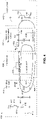
- FIG. 1 is a schematic diagram of a portion of circuitry 100 that may include an amplifier circuit.
- the circuitry 100 may include an amplifier circuit 124, which may be a switching amplifier that may be configured to receive a square wave and output a sine wave to be provided to a load circuit 150.
- the amplifier circuit 124 is shown as a class E amplifier, however, as will be described in greater detail below, the operation of the class E amplifier may be modified to what is referred to herein as class E2 in accordance with exemplary embodiments described herein, to improve amplifier performance.
- the amplifier circuit 124 may be driven by an input signal 102 from an oscillator (not shown).
- the amplifier circuit 124 may also be provided with a drive voltage V D that is configured to control the maximum power that may be delivered through the load circuit 150.
- the circuitry 100 may include a filter circuit 126.
- the filter circuit 126 may be a three pole (capacitor 134, inductor 132, and capacitor 136) low pass filter circuit 126, or any other filter
- the signal output by the filter circuit 126 may be provided to a load circuit 150.
- the load circuit may comprise an antenna 114.
- the load circuit 150 may include a series resonant circuit having a capacitance 120 (e.g., that may be due to the capacitance of the antenna or to an additional capacitor component) and inductance (e.g., that may be the inductance of the antenna) that may resonate at a frequency of the filtered signal provided by the amplifier circuit 124.
- the load of the load circuit 150 may be represented by the variable resistor 122.
- the load circuit 150 may be any one of a variety of circuits that are driven by the amplifier circuit 124 and the components shown in the load circuit 150 are for purposes of illustration with regards to FIG.
- the load circuit may be a resonator for generating a magnetic field
- the load of the load circuit represented by the variable resistor 122 may be the variation in load presented to the load circuit via one or more receivers coupling power via a magnetic field and thus changing the impedance at the resonator.
- FIG. 2 is a block diagram showing transmit circuitry 200 using a class E amplifier circuit for a wireless power application.
- the transmit circuitry 200 comprises an amplifier circuit 210, an impedance transformation circuit 230 and a load circuit 240.
- the transmit circuitry 200 also comprises a harmonics element 220.
- the harmonics element 220 can be generally characterized by a function 222 that is an open circuit at all harmonics of the fundamental frequency, f1 .
- the fundamental frequency, f1 may be a fundamental power transfer frequency of, for example, 6.78 MHz.
- the amplifier circuit 210 comprises a switch 216 coupled to a node 211.
- the node 211 is also coupled to a voltage source, Vpa (V power amplifier), 212 through an inductor 214.
- the inductor 214 may be referred to as Lchoke.
- the switch 216 may comprise a semiconductor switch, and may comprise one or more transistors fabricated using any of a variety of technologies.
- the diode 217 may comprise the body diode of a transistor that comprises the switch 216.
- the amplifier circuit 210 may also comprises a shunt capacitance 218.
- the capacitance 218 may comprise the capacitance of the switch 216, may comprise a capacitance that is greater than the capacitance of the switch 216, or may comprise a variable capacitance.
- the capacitance 218 may be referred to as a shunt capacitance, Cs.
- the impedance transformation circuit 230 comprises inductor L1 232, a first capacitor C1 236, a second capacitor C2 234, and part or all of inductor 242.
- the load circuit 240 comprises part or all of inductor 242 and a resistor 244.
- the load circuit 240 may comprise some or all of a resonant circuit, and if configured as a resonant circuit, may also be referred to as a resonator. If the load circuit 240 is part of a resonant circuit, the inductor 242 may be referred to as Lres and the resistor 244 may be referred to as Rres.
- the resistor 244 may comprise the resistance of the inductor 242 as well as the magnetically coupled load in the load circuit 240.
- An input signal 215 may be provided to the switch 216.
- the input signal 215 may comprise a signal that may control the switch 216 to be off (open, or non-conductive) approximately 50% of the cycle of the input signal 215, and may control the switch 216 to be on (closed, or conductive) approximately 50% of the cycle of the input signal 215.
- This on/off cycle can also be referred to as a nominal 50% duty cycle.
- the class E amplifier circuit 210 may characterized by having an optimal load, Zload, that is inductive at the fundamental frequency, f1, and that presents high impedance to the amplifier circuit 210 at all harmonics of the fundamental frequency, f1.
- the function 222 being generally open at harmonics of the fundamental frequency, f1 is generally achieved by the use of resonant networks.
- the waveshape of the amplifier circuit 210 approximates a half sine wave with a 50% on/off cycle.
- FIG. 3 is a block diagram showing transmit circuitry 300 using a class F amplifier circuit for a wireless power application.
- the transmit circuitry 300 comprises an amplifier circuit 310, an impedance transformation circuit 330 and a load circuit 340.
- the transmit circuitry 300 also comprises a harmonics element 320.
- the harmonics element 320 can be generally characterized by a function 322 that is an open circuit at odd harmonics of the fundamental frequency, f1 and a function 323 that is a short circuit at even harmonics of the fundamental frequency, f1, reflecting even harmonic energy back to the switch.
- the fundamental frequency, f1 may be a fundamental power transfer frequency of, for example, 6.78 MHz.
- the amplifier circuit 310 comprises a switch 316 coupled to a node 311.
- the node 311 is also coupled to a voltage source, Vpa (V power amplifier) 312 through an inductor 314.
- the inductor 314 may be referred to as Lchoke.
- the switch 316 may comprise a semiconductor switch, and may comprise one or more transistors fabricated using any of a variety of technologies.
- the diode 317 may comprise the body diode of a transistor that comprises the switch 316.
- the amplifier circuit 310 may also comprises a shunt capacitance 318.
- the capacitance 318 may comprise the capacitance of the switch 316, may comprise a capacitance that is greater than the capacitance of the switch 316, or may comprise a variable capacitance.
- the capacitance 318 may be referred to as a shunt capacitance, Cs.
- the impedance transformation circuit 330 comprises inductor L1 332, a first capacitor C1 336, a second capacitor C2 334, and part or all of inductor 342.
- the load circuit 340 comprises part or all of inductor 342 and a resistor 344.
- the load circuit 340 may comprise some or all of a resonant circuit, and if configured as a resonant circuit, may also be referred to as a resonator. If the load circuit 340 is part of a resonant circuit, the inductor 342 may be referred to as Lres and the resistor 344 may be referred to as Rres.
- the resistor 344 may comprise the resistance of the inductor 342 as well as the magnetically coupled load in the load circuit 340.
- An input signal 315 may be provided to the switch 316.
- the input signal 315 may comprise a signal that may control the switch 316 to be off (open, or non-conductive) approximately 50% of the cycle of the input signal 315, and may control the switch 316 to be on (closed, or conductive) approximately 50% of the cycle of the input signal 315.
- the class F amplifier circuit 310 may characterized by having an optimal load, Zload, that is inductive at the fundamental frequency, f1 , and that presents high impedance to the amplifier circuit 310 at odd harmonics of the fundamental frequency, f1 and that presents a low impedance to the amplifier circuit 310 at even harmonics fundamental frequency, f1 .
- the function 322 being generally an open circuit at odd harmonics and the function 323 being generally a short circuit at even harmonics is generally achieved by the use of resonant networks.
- the waveshape of the amplifier circuit 310 approximates a rectangular wave with a 50% on/off cycle.
- FIG. 4 is a block diagram showing an exemplary embodiment of circuitry 400 using a class E2 amplifier circuit.
- the circuit 400 may comprise part of transmit circuitry for a wireless power transfer application; however, the amplifier circuit described in FIG. 4 is applicable to any amplifier application in which the effects of load variation are sought to be minimized and where a predominantly positive load reactance at the second harmonic is desired.
- the transmit circuitry 400 comprises an amplifier circuit 410, an impedance transformation circuit 430 and a load circuit 440.
- the transmit circuitry 400 also comprises a harmonics element 420; however, while shown as a distinct physical inductance element 422, in a practical implementation, the harmonics element 420 may also comprise the inductance of the inductor 422 optionally series combined with an inductance of an inductor 432 as a single element having the sum of the two inductances 422 and 432.
- the fundamental frequency, f1 may be a fundamental power transfer frequency of, for example, 6.78 MHz and the second harmonic, f 2, thereof may be at a frequency of 13.56 MHz.
- the amplifier circuit 410 is configured as a class E2 amplifier configured to operate at the second harmonic, f 2, of the fundamental frequency. It should be appreciated that other fundamental frequencies and second harmonics are also contemplated.
- the amplifier circuit 410 comprises a switch 416 coupled to a node 411.
- the node 411 is also coupled to a voltage source, V PA (V power amplifier) 412 through an inductor 414.
- the inductor 414 may be referred to as Lchoke.
- the switch 416 may comprise a semiconductor switch, and may comprise one or more transistors fabricated using any of a variety of technologies.
- the amplifier circuit 410 also comprises an optional diode 417 and a shunt capacitance 418.
- the diode 417 may comprise the body diode of a transistor that comprises the switch 416.
- the capacitance 418 may comprise the capacitance of the switch 416, may comprise a capacitance that is greater than the capacitance of the switch 416, or may comprise a variable capacitance.
- the capacitance 418 may be referred to as a shunt capacitance, Cs.
- the impedance transformation circuit 430 may comprise a filter circuit comprising the inductance of the inductor 422, the inductor L1 432, a first capacitor C1 436, a second capacitor C2 434, and part or all of inductor 442.
- the load circuit 440 comprises part or all of inductor 442 and a resistor 444.
- the load circuit 440 may comprise some or all of a resonant circuit, and in an exemplary embodiment, may also be referred to as a resonator.
- the inductor 442 may be referred to as Lres and the resistor 444 may be referred to as Rres.
- the resistor 444 may comprise the resistance of the inductor 442 as well as a magnetically coupled load in the load circuit 440.
- an input signal 415 is provided to the switch 416.
- the input signal 415 comprises a signal that controls the switch 416 to be off (open, or non-conductive) approximately 25% of the cycle of the input signal 415, and controls the switch 416 to be on (closed, or conductive) approximately 75% of the cycle of the input signal 415.
- This is referred to as a nominal 25% duty cycle.
- a nominal 25% duty cycle may include a duty cycle where the switch 416 may be off (open, or non-conductive) approximately 20% or less of the cycle of the input signal 415, and where the switch 416 may be on (closed, or conductive) approximately 70% or more of the cycle of the input signal 415.
- the input signal 415 may comprise a transmit signal at a fundamental power transmit frequency, f1 .
- the impedance presented at Zload, interfacing at the inductor 422 represents an operative state in which the harmonics element 420 is resonant with capacitance 418 at approximately the second harmonic ( f2 ) of the fundamental frequency, f1 .
- the fundamental frequency, f1 may be 6.78 MHz and the second harmonic thereof may be at a frequency of 13.56 MHz.
- the circuit comprising the inductor 422, the inductor L1 432, the first capacitor C1 436, the second capacitor C2 434, together with at least a part of the inductor 442 form a 1 ⁇ 4 wave transformation circuit 451 at the fundamental frequency, f1.
- the 1 ⁇ 4 wave transformation circuit 451 together with the capacitance 418 in the amplifier circuit 410 also forms a resonant circuit at approximately the second harmonic, f 2, of the fundamental frequency, f1. This second harmonic resonance substantially contributes to satisfy zero voltage switching (ZVS) conditions at the nominal 25% switching point.
- ZVS zero voltage switching
- the inductor 442 is characterized predominantly as a positive reactance.
- the reactance of inductor L1 432 doubles, the reactance of the first capacitor C1 436 is halved, and the coupling of the amplifier circuit 410 to the load circuit 440 is greatly diminished in terms of impedance variation presented to the amplifier circuit 410. Therefore, at a given load, the impedance presented to the amplifier circuit 410 is dominated by impedances at f2 and less impacted by load variations at the 1 ⁇ 4 wave transformation circuit 451.
- the impedance transformation circuit 430 strongly couples the resonator impedance to Z LOAD at the fundamental, f1 , but weakly couples the resonator impedance to Z LOAD at harmonics, such as at /2. This makes the second harmonic current relatively insensitive to resonator impedance, and consequentially makes the waveshape at the switch less sensitive to output load variations at the fundamental frequency, f1.
- the inductance of the representative inductor 422 can be combined as part of the total inductance of the 1 ⁇ 4 wave transformation circuit 451 at the second harmonic, f 2, of the fundamental frequency, f1 , such that with an approximate nominal 25% off / 75% on cycle, a current is circulated through the transmit circuitry 400 at the second harmonic, f 2, of the fundamental frequency, f1 .
- the current that circulates through the transmit circuitry 400 at the second harmonic, f2 is represented by the current loop 462, whereby the current at f 2 substantially passes through the circuitry comprising the capacitor 418, the inductor 432 and the capacitor 436.
- the current at f 2 shown by the current loop 462 is substantially attenuated to the resistor 444, thus minimizing output energy at the second harmonic f2 of the fundamental frequency.
- controlling the switch 416 using an approximate nominal 25% off / 75% on cycle together with choosing the values of the capacitor 418, inductor 422, inductor L1 432, and first capacitor C1 436 to be resonant at the second harmonic, f 2, of the fundamental frequency, f1, allows a return current, shown by the current loop 462, to circulate as stored energy through the transmit circuitry 400 at the second harmonic, f2 .
- Circulating a return current through the transmit circuitry 400 at the second harmonic, f 2 substantially improves efficiency and allows a significantly wider reactance range as compared to certain other configurations of class E or class F amplifiers.
- the current that circulates through the transmit circuitry 400 at the fundamental frequency, f1 is represented by the current loop 464, whereby the current at f1 substantially passes through the circuitry comprising the capacitor 418, the inductor 422, the inductor 432, the capacitor 434, the inductor 442 and the resistor 444.
- a power transmit signal at the fundamental frequency, f1, shown by the current loop 464 is wirelessly transmitted by the inductor 442 and the resistor 444.
- the switch 416 is presented with a resonance at the second harmonic f 2 that minimally couples the amplifier circuit 410 to the load circuit 440 (shown by current loop 462 not circulating current in the inductor 442 or the resistor 444), thus serving to shape the switching waveform with what is referred to as "zero voltage switching" qualities.
- the f 1 current component is strongly coupled to the output for the purpose of delivering RF power at f 1 (shown by the current loop 464 that circulates current in the inductor 442 and the resistor 444).
- the f 2 current component is primarily reflected back to the switch 416 at the capacitor 436, thus forming a moderately high Q resonance toward the switch 416 in the current loop 462 and significantly attenuating the f 2 component toward the inductor 442 and the resistor 444.
- the class E2 amplifier circuit 410 may characterized by having an optimal load, Zload, that is inductive at the fundamental frequency, f1, and at the second harmonic, f 2, of the fundamental frequency, f1.
- the waveshape of the amplifier circuit 410 approximates a half-sine wave with an approximate nominal 25% off / 75% on cycle.
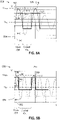
- FIG. 5A is a graphical diagram 500 showing an output waveform of an exemplary class E amplifier circuit.
- the horizontal axis 502 shows time increasing to the right and the vertical axis 504 shows the voltage at node 211 ( FIG. 2 ).
- the waveform 506 has a first portion 508 shown in solid line that shows the voltage at the node 211 when the switch 216 is open, or non-conductive, and has a second portion 509 shown in dotted line that shows the voltage at the node 211 had the switch 216 remained open.
- the switching period of one cycle of the switch 216 is shown using reference numeral 511.
- the time 512 illustrates a switching time at which the switch 216 transitions from being open, or non-conductive, to being closed, or conductive.
- the second portion 509 of the waveform 506 illustrates the natural decay of the waveform 506 to the voltage V PA had the switch 216 not been closed at time 512.
- the waveform 516 and switching period 521 show the voltage at node 211 for a subsequent cycle with the portion of the waveform 516 as normal operation.
- the second portion 509 of the waveform 506 can exhibit a relatively fast decay to V PA because at the fundamental frequency, substantial energy from the amplifier circuit 210 is lost to the load resistor 244.
- FIG. 5B is a graphical diagram 550 showing an output waveform of an exemplary class E2 amplifier circuit.
- the horizontal axis 552 shows time increasing to the right and the vertical axis 554 shows the voltage at node 411 ( FIG. 4 ).
- the waveform 556 has a first portion 558 that shows the voltage at the node 411 when the switch 416 is open, or non-conductive, and has a second portion 559 that shows the voltage at the node 411 had the switch 416 remained open.
- the switching period of one cycle of the switch 416 is shown using reference numeral 561.
- the time 562 illustrates a switching time at which the switch 416 transitions from being open, or non-conductive, to being closed, or conductive.
- the second portion 559 of the waveform 556 illustrates the decay of the waveform 556 to V PA had the switch 416 not been closed at time 562, and shows a relatively slower time constant as compared to the second portion 509 of the waveform 506 of FIG. 5A .
- the waveform 566 and switching period 572 show the voltage at node 411 for a subsequent cycle with the portion of the waveform 566 as normal operation.
- the slower decay of the waveform portion 559 illustrates lower losses at the second harmonic ( f 2) as the current at the second harmonic, f 2, is minimally coupled to the load circuit 440, and is instead substantially circulated in the amplifier circuit 410 as described above.
- 5B are illustrative examples of the switching characteristics of a class E and a class E2 amplifier circuit, respectively, at a particular load and are subject to differences based on a number of factors including, for example only, load, the amount of loss in the circuitry, and other factors.
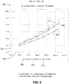
- FIG. 6 is a graphical diagram 600 comparing theoretical 100% efficiency contours of a class E and a class E2 amplifier circuit.
- the horizontal axis 602 shows Zload reactance (jXL) and the vertical axis 604 shows Zload resistance (RL).
- the trace 616 shows the 100% efficiency contour of a class E amplifier for reference with zero circulating current at harmonics of the fundamental frequency.
- the right-hand portion 618 of the trace 616 shows the practical efficiency of a class E amplifier with circulating current at second and higher harmonics.
- the traces 606, 608, 610 and 612 are all substantially centered around the zero (0) reactance point, showing that there is a +/- reactance range associated with the class E2 amplifier within which the class E2 amplifier may efficiently operate.
- a Class E2 amplifier operates at a nominal 25% duty cycle, where the switch (416, FIG. 4 ) conducts approximately 75% of the cycle and is off approximately 25% of the cycle, thus achieving optimum performance when the impedance at the load, Z LOAD , is centered at j0, thus supporting a +/- reactance range predominantly centered around the j0 point.
- the class E2 amplifier shifts the operating point where maximum efficiency is achieved at the center of the reactance range rather than the upper end of the reactance range, as shown by the trace 616.
- the class E2 amplifier supports a proportionally much wider reactance operating range compared to Class E and F amplifiers and also operates at a comparatively low input resistance, making it ideal for low voltage power supply operation.
- the class E2 design is based on the premise that fundamental and 2 nd harmonic current are intentionally presented at Z LOAD with exemplary embodiments as described above.
- FIG. 7 is a graphical diagram 700 showing an output waveform of the class E2 amplifier circuit of FIG. 4 .
- the horizontal axis 702 shows time increasing to the right and the vertical axis 704 shows the voltage at node 411 ( FIG. 4 ).
- the pulses 706 and 708 illustrate the periods of time when the switch 416 ( FIG. 4 ) is open (non-conductive).
- the load inductance formed by the 1 ⁇ 4 wave transformation circuit 451 ( FIG. 4 ) at the second harmonic, f 2, of the fundamental frequency, f1 in parallel with the capacitance C S 418 sets a waveform that forms a near half sine wave, which intercepts zero voltage at a nominal 25% duty cycle (the switch 416 is off approximately 25% of the time).
- the waveform is substantially satisfied by the second harmonic and only secondarily affected by load impedance at the fundamental.
- certain class E and class F amplifiers substantially satisfy the waveform requirements at the fundamental frequency, where second harmonic current degrades the shape of the waveform away from optimal performance.
- FIG. 8 is a graphical diagram 800 showing the magnitude of the impedance presented to the amplifier circuit 210, Zload as a function of load resistance and resonator impedance of a class E amplifier, where load magnitude is not centered and provides differing voltage and current stresses at each extreme of Zload reactance.
- the horizontal axis 802 shows the reactance of the resonator in the load circuit 240 ( FIG. 2 ) and the vertical axis 804 shows the impedance of the load (Zload).
- the graph 800 shows that for all three cases of RL, the highest impedance occurs at the high range of XL, while the lowest impedance occurs at the low range of XL.
- a high load impedance translates to low circulating currents at the transistor (switch 216) and RF inductor 214, while a low load impedance translates to higher circulating currents.
- the circulating currents are highest at low resonator reactance (XL), resulting in higher losses in the transistor (switch 416) and higher winding loss in the RF inductor 214.
- FIG. 9 is a graphical diagram 900 showing the magnitude of the impedance presented to the amplifier circuit 410, Zload as a function of load resistance and resonator impedance of a class E2 amplifier.
- load magnitude is centered and does allow comparable voltage and current stresses at each extreme of Zload reactance, effectively doubling the tolerable load impedance range compared to an equivalent class E amplifier.
- the horizontal axis 902 shows the reactance of the resonator in the load circuit 440 ( FIG. 4 ) and the vertical axis 904 shows the impedance of the load (Zload).
- the peak impedance occurs at the mid range of XL (approximately 80j ⁇ ) and tapers off to a lower impedance value at both ends of the traces 906, 908 and 910.
- a load resistance of RL 50 ⁇ , the circulating currents are almost the same across the entire XL range as shown by the trace 806.
- Z LOAD is higher in the nominal 25% duty cycle design implying lower circulating current in the transistor switch (switch 416, FIG. 4 ) and the RF inductor (414, FIG. 4 ) at nominal 25% duty cycle. Therefore, the losses should be lower using a nominal 25% duty cycle.
- the diagram 900 illustrates an approximate factor of two resonator reactance advantage when operating in class E2 amplification vs. class E.
- the class E2 amplifier presents a switch load that is approximately symmetrical from the center of the resonator reactance range.
- the load impedance of the class E amplifier increases with load reactance, consequentially, for the same the resonator reactance range, the switch is presented with approximately twice the load impedance variation.
- Advantages of a class E2 amplifier over certain class E amplifier configurations include, for example, improved efficiency above a threshold over a range of complex impedance values, expanded reactance range, low voltage operation (a factor of 1 ⁇ 2 to 1/3 in dc voltage when compared to class E), and reduced harmonic filter complexity due to only using series inductance.
- the circuitry 400 ( FIG. 4 ) need not provide full isolation at the second harmonic. It does however significantly reduce load variation at the second harmonic and presents a predominantly positive reactance to the amplifier circuit 410 at the second harmonic.
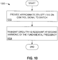
- FIG. 10 is a flowchart illustrating an exemplary embodiment of a method 1000 for operating a class E2 amplifier circuit as shown in Fig.4 .
- the blocks in the method 1000 can be performed in or out of the order shown.
- the description of the method 1000 will relate to the various embodiments described herein.
- a control signal having an approximate 25% off / 75% on cycle is provided to an amplifier circuit.
- the control signal is provided to a semiconductor switch, such as the switch 416 ( FIG. 4 ).
- transmit circuitry is approximately resonant at a frequency that is a second harmonic of a fundamental frequency such that a current circulates in the amplifier at a second harmonic of the fundamental frequency.
- the values of the components of the transmit circuitry are chosen such that the capacitor 418, inductor L1 432, and first capacitor C1 436, are resonant at the second harmonic, f 2, of the fundamental frequency, f1 .
- FIG. 11 is a functional block diagram of an apparatus 1100 for operating a class E2 amplifier circuit in a wireless power transmitter.
- the apparatus 1100 comprises means 1102 for providing a control signal having an approximate 25% off / 75% on cycle to the amplifier circuit.
- the means 1102 for providing a control signal having an approximate 25% off / 75% on cycle to the amplifier circuit is configured to perform the function described in operation block 1002 of method 1000 ( FIG. 10 ).
- the means 1102 for providing a control signal having an approximate 25% off / 75% on cycle to an amplifier circuit may comprise the input signal provided to the transmit circuitry described herein.
- the apparatus 1100 further comprises means 1104 for the transmit circuitry resonating at a frequency that is a second harmonic of a fundamental frequency.
- the means 1104 for the transmit circuitry resonating at a frequency that is a second harmonic of a fundamental frequency is configured to perform the functions described in operation block 1004 of method 1000 ( FIG. 10 ), including circulating a current in the amplifier at a second harmonic of the fundamental frequency as shown in Fig.4 .
- the means 1104 for transmit circuitry resonating at a frequency that is a second harmonic of a fundamental frequency comprises the transmit circuitry described herein.
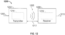
- FIG. 12 is a functional block diagram of an exemplary wireless power transfer system 1200, in which exemplary embodiments may be implemented.
- the exemplary wireless power transfer system 1200 is shown as one example of many applications for the class E2 amplifier circuit described herein, and is not intended to limit the application of the class E2 amplifier circuit in any of a number of applications.
- Wirelessly transferring power may refer to transferring any form of energy associated with electric fields, magnetic fields, electromagnetic fields, or otherwise from a transmitter to a receiver without the use of physical electrical conductors (e.g., power may be transferred through free space).
- the power output into a wireless field e.g., a magnetic field
- Input power 1202 may be provided to a transmitter 1204 from a power source (not shown) for generating a field 1205 (e.g., magnetic or species of electromagnetic) for providing energy transfer.
- a receiver 1208 may couple to the field 1205 and generate output power 1210 for storing or consumption by a device (not shown) coupled to the output power 1210. Both the transmitter 1204 and the receiver 1208 are separated by a distance 1212.
- transmitter 1204 and receiver 1208 are configured according to a mutual resonant relationship. When the resonant frequency of receiver 1208 and the resonant frequency of transmitter 1204 are substantially the same or very close, transmission losses between the transmitter 1204 and the receiver 1208 are reduced.
- wireless power transfer may be provided over larger distances in contrast to purely inductive solutions that may require large coils to be very close (e.g., millimeters).
- Resonant inductive coupling techniques may thus allow for improved efficiency and power transfer over various distances and with a variety of inductive coil configurations.
- the receiver 1208 may receive power when the receiver 1208 is located in an energy field 1205 produced by the transmitter 1204.
- the field 1205 corresponds to a region where energy output by the transmitter 1204 may be captured by a receiver 1208.
- the transmitter 1204 may include a transmit antenna 1214 (that may also be referred to herein as a coil) for outputting an energy transmission.
- the receiver 1208 further includes a receive antenna 1218 (that may also be referred to herein as a coil) for receiving or capturing energy from the energy transmission.
- the field 1205 may correspond to the "near-field" of the transmitter 1204.
- the near-field may correspond to a region in which there are strong reactive fields resulting from the currents and charges in the transmit antenna 1214 that minimally radiate power away from the transmit antenna 1214. In some cases the near-field may correspond to a region that is within about one wavelength (or a fraction thereof) of the transmit antenna 1214.
- the transmitter 1204 may be configured to output a time varying magnetic field 1205 with a frequency corresponding to the resonant frequency of the transmit antenna 1214.
- the time varying magnetic field 1205 may induce a voltage in the receive antenna 1218 that causes an electrical current to flow through the receive antenna 1218.
- the receive antenna 1218 is configured to be resonant at the frequency of the transmit antenna 1214, energy may be more efficiently transferred.
- the AC signal induced in the receive antenna 1118 may be rectified to produce a DC signal that may be provided to charge or to power a load.
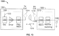
- FIG. 13 is a functional block diagram of exemplary components in a wireless power transfer system 1300 that may be used in the wireless power transfer system 1200 of FIG. 12 , in accordance with various exemplary embodiments.
- the transmitter 1304 may include transmit circuitry 1306 that may include an oscillator 1322, a driver circuit 1324, and a filter and matching circuit 1326.
- the oscillator 1322 may be configured to generate a signal at a desired frequency, such as 468.75 KHz, 6.78 MHz or 13.56 MHz, that may be adjusted in response to a frequency control signal 1323.
- the oscillator signal may be provided to a driver circuit 1324 configured to drive the transmit antenna 1314 at, for example, a resonant frequency of the transmit antenna 1314.
- the driver circuit 1324 is a switching amplifier configured to receive a square wave from the oscillator 1322 and output a sine wave.
- the driver circuit 1324 is a class E2 amplifier, as described herein.
- a filter and matching circuit 1326 is also included to filter out harmonics or other unwanted frequencies and match the impedance of the transmitter 1304 to the impedance of the transmit antenna 1314.
- the transmitter 1304 may wirelessly output power at a level sufficient for charging or powering an electronic device.
- the power provided may be for example on the order of 300 milliWatts to 5 Watts or 5 Watts to 40 Watts to power or charge different devices with different power requirements. Higher or lower power levels may also be provided.
- the receiver 1308 may include receive circuitry 1310 that may include a matching circuit 1332 and a rectifier and switching circuit 1334 to generate a DC power output from an AC power input to charge a battery 1336 as shown in FIG. 13 or to power a device (not shown) coupled to the receiver 1308.
- the matching circuit 1332 may be included to match the impedance of the receive circuitry 1310 to the impedance of the receive antenna 1318.
- the receiver 1308 and transmitter 1304 may additionally communicate on a separate communication channel 1319 (e.g., Bluetooth, zigbee, cellular, etc.).
- the receiver 1308 and transmitter 1304 may alternatively communicate via in-band signaling using characteristics of the wireless field 1305.
- the receiver 1308 may initially have a selectively disablable associated load (e.g., battery 1336), and may be configured to determine whether an amount of power transmitted by transmitter 1304 and received by receiver 1308 is appropriate for charging a battery 1336. Further, receiver 1308 may be configured to enable a load (e.g., battery 1336) upon determining that the amount of power is appropriate.
- a selectively disablable associated load e.g., battery 1336
- FIG. 14 is a schematic diagram of a portion of transmit circuitry 1306 or receive circuitry 1310 of FIG. 13 including a transmit or receive antenna 1452, in accordance with exemplary embodiments.
- transmit or receive circuitry 1450 used in exemplary embodiments including those described below may include an antenna 1452.
- the antenna 1452 may also be referred to or be configured as a "loop" antenna 1452.
- the antenna 1452 may also be referred to herein or be configured as a "magnetic" antenna or an induction coil.
- antenna 1452 generally refers to a component that may wirelessly output or receive energy for coupling to another "antenna.”
- the antenna 1452 may also be referred to as a coil of a type that is configured to wirelessly output or receive power.
- an antenna 1452 is an example of a "power transfer component" of a type that is configured to wirelessly output and/or receive power.
- the antenna 1452 may be configured to include an air core or a physical core such as a ferrite core (not shown).
- the antenna 1452 may form a portion of a resonant circuit configured to resonate at a resonant frequency.
- the resonant frequency of the loop or magnetic antenna 1452 is based on the inductance and capacitance. Inductance may be simply the inductance created by the antenna 1452, whereas, capacitance may be added to create a resonant structure (e.g., a capacitor may be electrically connected to the antenna 1452 in series or in parallel) at a desired resonant frequency.
- capacitor 1454 and capacitor 1456 may be added to the transmit or receive circuitry 1450 to create a resonant circuit that resonates at a desired frequency of operation.
- a capacitor (not shown) may be placed in parallel between the two terminals of the antenna 1452.
- a signal 1458 with a frequency that substantially corresponds to the resonant frequency of the antenna 1452 may be an input to the antenna 1452.
- the signal 1458 may be the output that may be rectified and used to power or charge a load.
- any suitable means capable of performing the operations such as various hardware and/or software component(s), circuits, and/or module(s).
- any operations illustrated in the Figures may be performed by corresponding functional means capable of performing the operations.
- the functions described may be implemented in hardware, software, firmware, or any combination thereof. If implemented in software, the functions may be stored on or transmitted as one or more instructions or code on a computer-readable medium.
- Computer-readable media include both computer storage media and communication media including any medium that facilitates transfer of a computer program from one place to another.
- a storage media may be any available media that may be accessed by a computer.
- such computer-readable media may comprise RAM, ROM, EEPROM, CD-ROM or other optical disk storage, magnetic disk storage or other magnetic storage devices, or any other medium that may be used to carry or store desired program code in the form of instructions or data structures and that may be accessed by a computer.
- any connection is properly termed a computer-readable medium.
- the software is transmitted from a website, server, or other remote source using a coaxial cable, fiber optic cable, twisted pair, digital subscriber line ("DSL"), or wireless technologies such as infrared, radio, and microwave
- coaxial cable, fiber optic cable, twisted pair, DSL, or wireless technologies such as infrared, radio, and microwave are included in the definition of medium.
- Disk and disc includes compact disc (“CD”), laser disc, optical disc, digital versatile disc (“DVD”), floppy disk and Blu-Ray disc where disks usually reproduce data magnetically, while discs reproduce data optically with lasers. Combinations of the above should also be included within the scope of computer-readable media.
Description
- This application claims the benefit of
U.S. Provisional Patent Application No. 62/266,747, entitled "Class E2 Amplifier," filed December 14, 2015 - The present disclosure relates generally power amplification. More specifically, the disclosure is directed to an amplifier comprising a class E2 amplifier circuit that can be used in a variety of applications, including wireless power transfer, and a corresponding method for operating the amplifier.
- Amplifiers and amplifier circuits are used in many different applications. Amplifiers and amplifier circuits that operate efficiently and that are insensitive to variations in load are desirable.
- Various implementations of amplifiers and methods within the scope of the appended claims each have several aspects, no single one of which is solely responsible for the desirable attributes described herein. Without limiting the scope of the appended claims, some prominent features are described herein.
- Details of one or more implementations of the subject matter described in this specification are set forth in the accompanying drawings and the description below. Other features, aspects, and advantages will become apparent from the description, the drawings, and the claims. Note that the relative dimensions of the following figures may not be drawn to scale.
- One aspect of the disclosure provides an amplifier as defined from
claim 1 to claim 11. - Another aspect of the disclosure provides a method for operating an amplifier as defined from claim 12 to 13.
- International Patent Application Publication No.
WO 2009/060264 A1 relates to an integrated circuit having harmonic termination circuitry.US Patent Application Publication No. US 2013/293189 A1 relates to a push-pull driver for generating a signal for wireless power transfer. Non-patent literature Kazimierczuk et al, 1987, relates to "Exact analysis of class E tuned power amplifier at any Q and switch duty cycle". - In the figures, like reference numerals refer to like parts throughout the various views unless otherwise indicated. For reference numerals with letter character designations such as "102a" or "102b", the letter character designations may differentiate two like parts or elements present in the same figure. Letter character designations for reference numerals may be omitted when it is intended that a reference numeral encompass all parts having the same reference numeral in all figures.
-
FIG. 1 is provided to aid with understanding the claimed invention, but is not corresponding to the claimed subject matter, and shows a schematic diagram of a portion of circuitry that may include an amplifier circuit. -
FIG. 2 is provided to aid with understanding the claimed invention, but is not corresponding to the claimed subject matter, and shows a block diagram showing transmit circuitry using a class E amplifier circuit for a wireless power application. -
FIG. 3 is provided to aid with understanding the claimed invention, but is not corresponding to the claimed subject matter, and shows a block diagram showing transmit circuitry using a class F amplifier circuit for a wireless power application. -
FIG. 4 is a block diagram showing an exemplary embodiment of circuitry using a class E2 amplifier circuit according to the claimed invention. -
FIG. 5A is provided to aid with understanding the claimed invention. but is not corresponding to the claimed subject matter, and shows a graphical diagram showing an output waveform of a class E amplifier circuit. -
FIG. 5B is a graphical diagram showing an output waveform of a class E2 amplifier circuit according to the claimed invention. -
FIG. 6 is a graphical diagram comparing theoretical 100% efficiency contours of a class E and a class E2 amplifier circuit according to the claimed invention. -
FIG. 7 is a graphical diagram showing an output waveform of the class E2 amplifier circuit ofFIG. 4 according to the claimed invention. -
FIG. 8 is provided to aid with understanding the claimed invention, but is not corresponding to the claimed subject matter, and shows a graphical diagram showing the magnitude of the impedance presented to the amplifier circuit, Zload as a function of load resistance and resonator impedance of a class E amplifier. -
FIG. 9 is a graphical diagram showing the magnitude of the impedance presented to the amplifier circuit, Zload as a function of load resistance and resonator impedance of a class E2 amplifier according to the claimed invention. -
FIG. 10 is a flowchart illustrating an exemplary embodiment of a method for operating a class E2 amplifier circuit according to the claimed invention in a wireless power transmitter. -
FIG. 11 is a functional block diagram of an apparatus for operating a class E2 amplifier circuit according to the claimed invention in a wireless power transmitter. -
FIG. 12 is a functional block diagram of an exemplary wireless power transfer system, in which exemplary embodiments of the class E2 amplifier circuit according to the present invention may be implemented. -
FIG. 13 is a functional block diagram of exemplary components in a wireless power transfer system that may be used in the wireless power transfer system ofFIG. 12 , in accordance with various exemplary embodiments of the class E2 amplifier circuit according to the present invention. -
FIG. 14 is a schematic diagram of a portion of transmit circuitry or receive circuitry ofFIG. 13 including a transmit or receive antenna, in accordance with exemplary embodiments of the class E2 amplifier circuit according to the present invention. - The various features illustrated in the drawings may not be drawn to scale. Accordingly, the dimensions of the various features may be arbitrarily expanded or reduced for clarity. In addition, some of the drawings may not depict all of the components of a given system, method or device. Finally, like reference numerals may be used to denote like features throughout the specification and figures.
- The detailed description set forth below in connection with the appended drawings is intended as a description of exemplary embodiments of the invention and is not intended to represent the only embodiments in which the invention may be practiced. The term "exemplary" used throughout this description means "serving as an example, instance, or illustration," and should not necessarily be construed as preferred or advantageous over other exemplary embodiments. The detailed description includes specific details for the purpose of providing a thorough understanding of the exemplary embodiments of the invention. In some instances, some devices are shown in block diagram form.
- In this description, the term "application" may also include files having executable content, such as: object code, scripts, byte code, markup language files, and patches. In addition, an "application" referred to herein, may also include files that are not executable in nature, such as documents that may need to be opened or other data files that need to be accessed.
- As used in this description, the terms "component," "database," "module," "system," and the like are intended to refer to a computer-related entity, either hardware, firmware, a combination of hardware and software, software, or software in execution. For example, a component may be, but is not limited to being, a process running on a processor, a processor, an object, an executable, a thread of execution, a program, and/or a computer. By way of illustration, both an application running on a computing device and the computing device may be a component. One or more components may reside within a process and/or thread of execution, and a component may be localized on one computer and/or distributed between two or more computers. In addition, these components may execute from various computer readable media having various data structures stored thereon. The components may communicate by way of local and/or remote processes such as in accordance with a signal having one or more data packets (e.g., data from one component interacting with another component in a local system, distributed system, and/or across a network such as the Internet with other systems by way of the signal).
- The disclosure describes a new class of amplifier, referred to as a class E2 amplifier that can be implemented to leverage the second harmonic of an input signal instead of the fundamental frequency of the input signal to satisfy wave shape requirements.
- In certain applications, amplifier circuits, referred to as 'class E' amplifier circuits are used to drive loads. For example, certain wireless power/charging systems may use class E amplifier circuits to drive a transmit antenna that may output energy for wirelessly coupling by one or more receivers (e.g., via driving the transmit antenna such as a coil with an alternating current to generate a magnetic field for inductively coupling power). More particularly, as an example, wireless charging systems achieve relatively high coupling by using transmitter and receiver coils tuned at or near resonance. Tuning the transmit and receive coils to a resonant frequency allows relatively high power transfer efficiencies without sacrificing device placement freedom or device size freedom. Further, it is desirable to maintain sufficient receiver power output while accommodating a wide variation in coupling and detuning effects due to variable positioning or other changing environmental conditions. Variable coupling and detuning effects cause changes in impedance and other characteristics at the transmit antenna.
- These impedance changes are reflected/presented to the circuit, such as a class E amplifier circuit, driving the transmit antenna. This may create difficulties in class E amplifier circuit design for efficiently driving such a load or other similar loads in various operating environments. For example, class E amplifiers may have a limited reactance range of which the amplifier is within a certain range of efficiency. The limitation on reactance range is due, at least in part, to reflected impedance from the load, significantly affecting the transmit wave shape at the transistor that forms the driver circuit of the power amplifier.
- Switchable or adjustable series reactance shifting networks may be used to at least somewhat alleviate the limited reactance range by operating the power amplifier over a narrower reactance range. This solution, however, may increase the number of components and may increase the cost of the amplifier or present other tradeoffs for configuring the amplifier circuit.
- In an exemplary embodiment, a new class of amplifier, referred to as a class E2 amplifier, can be implemented to leverage the second harmonic of a transmit signal instead of the fundamental frequency of the transmit signal to satisfy wave shape requirements. Satisfying wave shape requirements refers to the waveform output of the amplifier returning to zero to satisfy a zero voltage switching (ZVS) condition. For example, one advantage of using the second harmonic of the power transmit signal to satisfy wave shape requirements is that the ZVS condition can be met over a significantly wider range of load impedances as compared to other configurations of class E or F amplifiers.
-
FIG. 1 is a schematic diagram of a portion ofcircuitry 100 that may include an amplifier circuit. Thecircuitry 100 may include anamplifier circuit 124, which may be a switching amplifier that may be configured to receive a square wave and output a sine wave to be provided to aload circuit 150. Theamplifier circuit 124 is shown as a class E amplifier, however, as will be described in greater detail below, the operation of the class E amplifier may be modified to what is referred to herein as class E2 in accordance with exemplary embodiments described herein, to improve amplifier performance. Theamplifier circuit 124 may be driven by aninput signal 102 from an oscillator (not shown). Theamplifier circuit 124 may also be provided with a drive voltage VD that is configured to control the maximum power that may be delivered through theload circuit 150. To eliminate or reduce harmonics, thecircuitry 100 may include afilter circuit 126. Thefilter circuit 126 may be a three pole (capacitor 134,inductor 132, and capacitor 136) lowpass filter circuit 126, or any other filter circuit. - The signal output by the
filter circuit 126 may be provided to aload circuit 150. In a wireless power transfer embodiment, the load circuit may comprise anantenna 114. Theload circuit 150 may include a series resonant circuit having a capacitance 120 (e.g., that may be due to the capacitance of the antenna or to an additional capacitor component) and inductance (e.g., that may be the inductance of the antenna) that may resonate at a frequency of the filtered signal provided by theamplifier circuit 124. The load of theload circuit 150 may be represented by thevariable resistor 122. However, it is appreciated that theload circuit 150 may be any one of a variety of circuits that are driven by theamplifier circuit 124 and the components shown in theload circuit 150 are for purposes of illustration with regards toFIG. 1 . In addition, in a wireless power application, where the load circuit may be a resonator for generating a magnetic field, the load of the load circuit represented by thevariable resistor 122 may be the variation in load presented to the load circuit via one or more receivers coupling power via a magnetic field and thus changing the impedance at the resonator. -
FIG. 2 is a block diagram showing transmitcircuitry 200 using a class E amplifier circuit for a wireless power application. The transmitcircuitry 200 comprises anamplifier circuit 210, animpedance transformation circuit 230 and aload circuit 240. The transmitcircuitry 200 also comprises aharmonics element 220. In a classE amplifier circuit 210 configured to operate at the fundamental frequency f1, theharmonics element 220 can be generally characterized by afunction 222 that is an open circuit at all harmonics of the fundamental frequency, f1. As an example, the fundamental frequency, f1, may be a fundamental power transfer frequency of, for example, 6.78 MHz. - The
amplifier circuit 210 comprises aswitch 216 coupled to anode 211. Thenode 211 is also coupled to a voltage source, Vpa (V power amplifier), 212 through aninductor 214. Theinductor 214 may be referred to as Lchoke. Theswitch 216 may comprise a semiconductor switch, and may comprise one or more transistors fabricated using any of a variety of technologies. In an exemplary embodiment, thediode 217 may comprise the body diode of a transistor that comprises theswitch 216. Theamplifier circuit 210 may also comprises ashunt capacitance 218. Thecapacitance 218 may comprise the capacitance of theswitch 216, may comprise a capacitance that is greater than the capacitance of theswitch 216, or may comprise a variable capacitance. Thecapacitance 218 may be referred to as a shunt capacitance, Cs. - The
impedance transformation circuit 230 comprisesinductor L1 232, afirst capacitor C1 236, asecond capacitor C2 234, and part or all ofinductor 242. - The
load circuit 240 comprises part or all ofinductor 242 and aresistor 244. Theload circuit 240 may comprise some or all of a resonant circuit, and if configured as a resonant circuit, may also be referred to as a resonator. If theload circuit 240 is part of a resonant circuit, theinductor 242 may be referred to as Lres and theresistor 244 may be referred to as Rres. Theresistor 244 may comprise the resistance of theinductor 242 as well as the magnetically coupled load in theload circuit 240. - An
input signal 215 may be provided to theswitch 216. In accordance with class E operation, theinput signal 215 may comprise a signal that may control theswitch 216 to be off (open, or non-conductive) approximately 50% of the cycle of theinput signal 215, and may control theswitch 216 to be on (closed, or conductive) approximately 50% of the cycle of theinput signal 215. This on/off cycle can also be referred to as a nominal 50% duty cycle. The classE amplifier circuit 210 may characterized by having an optimal load, Zload, that is inductive at the fundamental frequency, f1, and that presents high impedance to theamplifier circuit 210 at all harmonics of the fundamental frequency, f1. Thefunction 222 being generally open at harmonics of the fundamental frequency, f1 is generally achieved by the use of resonant networks. The waveshape of theamplifier circuit 210 approximates a half sine wave with a 50% on/off cycle. -
FIG. 3 is a block diagram showing transmitcircuitry 300 using a class F amplifier circuit for a wireless power application. The transmitcircuitry 300 comprises anamplifier circuit 310, animpedance transformation circuit 330 and aload circuit 340. The transmitcircuitry 300 also comprises aharmonics element 320. In a classF amplifier circuit 310 configured to operate at the fundamental frequency f1, theharmonics element 320 can be generally characterized by afunction 322 that is an open circuit at odd harmonics of the fundamental frequency, f1 and afunction 323 that is a short circuit at even harmonics of the fundamental frequency, f1, reflecting even harmonic energy back to the switch. The fundamental frequency, f1, may be a fundamental power transfer frequency of, for example, 6.78 MHz. - The
amplifier circuit 310 comprises aswitch 316 coupled to anode 311. Thenode 311 is also coupled to a voltage source, Vpa (V power amplifier) 312 through aninductor 314. Theinductor 314 may be referred to as Lchoke. Theswitch 316 may comprise a semiconductor switch, and may comprise one or more transistors fabricated using any of a variety of technologies. In an exemplary embodiment, thediode 317 may comprise the body diode of a transistor that comprises theswitch 316. Theamplifier circuit 310 may also comprises ashunt capacitance 318. Thecapacitance 318 may comprise the capacitance of theswitch 316, may comprise a capacitance that is greater than the capacitance of theswitch 316, or may comprise a variable capacitance. Thecapacitance 318 may be referred to as a shunt capacitance, Cs. - The
impedance transformation circuit 330 comprisesinductor L1 332, afirst capacitor C1 336, asecond capacitor C2 334, and part or all ofinductor 342. - The
load circuit 340 comprises part or all ofinductor 342 and aresistor 344. Theload circuit 340 may comprise some or all of a resonant circuit, and if configured as a resonant circuit, may also be referred to as a resonator. If theload circuit 340 is part of a resonant circuit, theinductor 342 may be referred to as Lres and theresistor 344 may be referred to as Rres. Theresistor 344 may comprise the resistance of theinductor 342 as well as the magnetically coupled load in theload circuit 340. - An
input signal 315 may be provided to theswitch 316. In accordance with class F operation, theinput signal 315 may comprise a signal that may control theswitch 316 to be off (open, or non-conductive) approximately 50% of the cycle of theinput signal 315, and may control theswitch 316 to be on (closed, or conductive) approximately 50% of the cycle of theinput signal 315. The classF amplifier circuit 310 may characterized by having an optimal load, Zload, that is inductive at the fundamental frequency, f1, and that presents high impedance to theamplifier circuit 310 at odd harmonics of the fundamental frequency, f1 and that presents a low impedance to theamplifier circuit 310 at even harmonics fundamental frequency, f1. Thefunction 322 being generally an open circuit at odd harmonics and thefunction 323 being generally a short circuit at even harmonics is generally achieved by the use of resonant networks. The waveshape of theamplifier circuit 310 approximates a rectangular wave with a 50% on/off cycle. -
FIG. 4 is a block diagram showing an exemplary embodiment ofcircuitry 400 using a class E2 amplifier circuit. In an exemplary embodiment, thecircuit 400 may comprise part of transmit circuitry for a wireless power transfer application; however, the amplifier circuit described inFIG. 4 is applicable to any amplifier application in which the effects of load variation are sought to be minimized and where a predominantly positive load reactance at the second harmonic is desired. - The transmit
circuitry 400 comprises anamplifier circuit 410, animpedance transformation circuit 430 and aload circuit 440. The transmitcircuitry 400 also comprises aharmonics element 420; however, while shown as a distinctphysical inductance element 422, in a practical implementation, theharmonics element 420 may also comprise the inductance of theinductor 422 optionally series combined with an inductance of aninductor 432 as a single element having the sum of the twoinductances amplifier circuit 410 is configured as a class E2 amplifier configured to operate at the second harmonic, f2, of the fundamental frequency. It should be appreciated that other fundamental frequencies and second harmonics are also contemplated. - In an exemplary embodiment, the
amplifier circuit 410 comprises aswitch 416 coupled to anode 411. Thenode 411 is also coupled to a voltage source, VPA (V power amplifier) 412 through aninductor 414. Theinductor 414 may be referred to as Lchoke. In an exemplary embodiment, theswitch 416 may comprise a semiconductor switch, and may comprise one or more transistors fabricated using any of a variety of technologies. Theamplifier circuit 410 also comprises anoptional diode 417 and ashunt capacitance 418. In an exemplary embodiment, thediode 417 may comprise the body diode of a transistor that comprises theswitch 416. Thecapacitance 418 may comprise the capacitance of theswitch 416, may comprise a capacitance that is greater than the capacitance of theswitch 416, or may comprise a variable capacitance. In an exemplary embodiment, thecapacitance 418 may be referred to as a shunt capacitance, Cs. - In an exemplary embodiment, the
impedance transformation circuit 430 may comprise a filter circuit comprising the inductance of theinductor 422, theinductor L1 432, afirst capacitor C1 436, asecond capacitor C2 434, and part or all ofinductor 442. - In an exemplary embodiment, the
load circuit 440 comprises part or all ofinductor 442 and aresistor 444. In an exemplary embodiment, theload circuit 440 may comprise some or all of a resonant circuit, and in an exemplary embodiment, may also be referred to as a resonator. In an exemplary embodiment in which theload circuit 440 is part of a resonant circuit, theinductor 442 may be referred to as Lres and theresistor 444 may be referred to as Rres. Theresistor 444 may comprise the resistance of theinductor 442 as well as a magnetically coupled load in theload circuit 440. - In an exemplary embodiment, an
input signal 415 is provided to theswitch 416. In an exemplary embodiment, theinput signal 415 comprises a signal that controls theswitch 416 to be off (open, or non-conductive) approximately 25% of the cycle of theinput signal 415, and controls theswitch 416 to be on (closed, or conductive) approximately 75% of the cycle of theinput signal 415. This is referred to as a nominal 25% duty cycle. A nominal 25% duty cycle may include a duty cycle where theswitch 416 may be off (open, or non-conductive) approximately 20% or less of the cycle of theinput signal 415, and where theswitch 416 may be on (closed, or conductive) approximately 70% or more of the cycle of theinput signal 415. In an exemplary embodiment, theinput signal 415 may comprise a transmit signal at a fundamental power transmit frequency, f1. - In an exemplary embodiment, the impedance presented at Zload, interfacing at the
inductor 422 represents an operative state in which theharmonics element 420 is resonant withcapacitance 418 at approximately the second harmonic (f2) of the fundamental frequency, f1. In an exemplary embodiment, the fundamental frequency, f1, may be 6.78 MHz and the second harmonic thereof may be at a frequency of 13.56 MHz. - In an exemplary embodiment, the circuit comprising the
inductor 422, theinductor L1 432, thefirst capacitor C1 436, thesecond capacitor C2 434, together with at least a part of theinductor 442 form a ¼wave transformation circuit 451 at the fundamental frequency, f1. Additionally, the ¼wave transformation circuit 451 together with thecapacitance 418 in theamplifier circuit 410 also forms a resonant circuit at approximately the second harmonic, f2, of the fundamental frequency, f1. This second harmonic resonance substantially contributes to satisfy zero voltage switching (ZVS) conditions at the nominal 25% switching point. - In an exemplary embodiment, at the second harmonic, f2, of the fundamental frequency, f1, the
inductor 442 is characterized predominantly as a positive reactance. Compared with the impedance at the fundamental frequency, f1, at the second harmonic, f2, the reactance ofinductor L1 432 doubles, the reactance of thefirst capacitor C1 436 is halved, and the coupling of theamplifier circuit 410 to theload circuit 440 is greatly diminished in terms of impedance variation presented to theamplifier circuit 410. Therefore, at a given load, the impedance presented to theamplifier circuit 410 is dominated by impedances at f2 and less impacted by load variations at the ¼wave transformation circuit 451. Theimpedance transformation circuit 430 strongly couples the resonator impedance to ZLOAD at the fundamental, f1, but weakly couples the resonator impedance to ZLOAD at harmonics, such as at /2. This makes the second harmonic current relatively insensitive to resonator impedance, and consequentially makes the waveshape at the switch less sensitive to output load variations at the fundamental frequency, f1. - The inductance of the
representative inductor 422 can be combined as part of the total inductance of the ¼wave transformation circuit 451 at the second harmonic, f2, of the fundamental frequency, f1, such that with an approximate nominal 25% off / 75% on cycle, a current is circulated through the transmitcircuitry 400 at the second harmonic, f2, of the fundamental frequency, f1. The current that circulates through the transmitcircuitry 400 at the second harmonic, f2, is represented by thecurrent loop 462, whereby the current at f2 substantially passes through the circuitry comprising thecapacitor 418, theinductor 432 and thecapacitor 436. The current at f2 shown by thecurrent loop 462 is substantially attenuated to theresistor 444, thus minimizing output energy at the second harmonic f2 of the fundamental frequency. - In an exemplary embodiment, controlling the
switch 416 using an approximate nominal 25% off / 75% on cycle, together with choosing the values of thecapacitor 418,inductor 422,inductor L1 432, andfirst capacitor C1 436 to be resonant at the second harmonic, f2, of the fundamental frequency, f1, allows a return current, shown by thecurrent loop 462, to circulate as stored energy through the transmitcircuitry 400 at the second harmonic, f2. Circulating a return current through the transmitcircuitry 400 at the second harmonic, f2, substantially improves efficiency and allows a significantly wider reactance range as compared to certain other configurations of class E or class F amplifiers. While the current at the second harmonic, f2, primarily circulates through the transmitcircuitry 400 as shown by thecurrent loop 462, a current also circulates through the transmitcircuitry 400 at the fundamental frequency, f1. The current that circulates through the transmitcircuitry 400 at the fundamental frequency, f1, is represented by thecurrent loop 464, whereby the current at f1 substantially passes through the circuitry comprising thecapacitor 418, theinductor 422, theinductor 432, thecapacitor 434, theinductor 442 and theresistor 444. In this manner, in an exemplary embodiment, a power transmit signal at the fundamental frequency, f1, shown by thecurrent loop 464, is wirelessly transmitted by theinductor 442 and theresistor 444. - In an exemplary embodiment, the
switch 416 is presented with a resonance at the second harmonic f2 that minimally couples theamplifier circuit 410 to the load circuit 440 (shown bycurrent loop 462 not circulating current in theinductor 442 or the resistor 444), thus serving to shape the switching waveform with what is referred to as "zero voltage switching" qualities. In contrast, the f1 current component is strongly coupled to the output for the purpose of delivering RF power at f1 (shown by thecurrent loop 464 that circulates current in theinductor 442 and the resistor 444). Topologically, the f2 current component is primarily reflected back to theswitch 416 at thecapacitor 436, thus forming a moderately high Q resonance toward theswitch 416 in thecurrent loop 462 and significantly attenuating the f2 component toward theinductor 442 and theresistor 444. - The class
E2 amplifier circuit 410 may characterized by having an optimal load, Zload, that is inductive at the fundamental frequency, f1, and at the second harmonic, f2, of the fundamental frequency, f1. The waveshape of theamplifier circuit 410 approximates a half-sine wave with an approximate nominal 25% off / 75% on cycle. -
FIG. 5A is a graphical diagram 500 showing an output waveform of an exemplary class E amplifier circuit. Thehorizontal axis 502 shows time increasing to the right and thevertical axis 504 shows the voltage at node 211 (FIG. 2 ). Thewaveform 506 has a first portion 508 shown in solid line that shows the voltage at thenode 211 when theswitch 216 is open, or non-conductive, and has asecond portion 509 shown in dotted line that shows the voltage at thenode 211 had theswitch 216 remained open. The switching period of one cycle of theswitch 216 is shown usingreference numeral 511. Thetime 512 illustrates a switching time at which theswitch 216 transitions from being open, or non-conductive, to being closed, or conductive. Thesecond portion 509 of thewaveform 506 illustrates the natural decay of thewaveform 506 to the voltage VPA had theswitch 216 not been closed attime 512. Thewaveform 516 and switchingperiod 521 show the voltage atnode 211 for a subsequent cycle with the portion of thewaveform 516 as normal operation. Thesecond portion 509 of thewaveform 506 can exhibit a relatively fast decay to VPA because at the fundamental frequency, substantial energy from theamplifier circuit 210 is lost to theload resistor 244. -
FIG. 5B is a graphical diagram 550 showing an output waveform of an exemplary class E2 amplifier circuit. Thehorizontal axis 552 shows time increasing to the right and thevertical axis 554 shows the voltage at node 411 (FIG. 4 ). Thewaveform 556 has afirst portion 558 that shows the voltage at thenode 411 when theswitch 416 is open, or non-conductive, and has asecond portion 559 that shows the voltage at thenode 411 had theswitch 416 remained open. The switching period of one cycle of theswitch 416 is shown usingreference numeral 561. Thetime 562 illustrates a switching time at which theswitch 416 transitions from being open, or non-conductive, to being closed, or conductive. Thesecond portion 559 of thewaveform 556 illustrates the decay of thewaveform 556 to VPA had theswitch 416 not been closed attime 562, and shows a relatively slower time constant as compared to thesecond portion 509 of thewaveform 506 ofFIG. 5A . Thewaveform 566 and switchingperiod 572 show the voltage atnode 411 for a subsequent cycle with the portion of thewaveform 566 as normal operation. The slower decay of thewaveform portion 559 illustrates lower losses at the second harmonic (f2) as the current at the second harmonic, f2, is minimally coupled to theload circuit 440, and is instead substantially circulated in theamplifier circuit 410 as described above. Using the second harmonic of the fundamental frequency to satisfy wave shape requirements and allowing the zero voltage switching (ZVS) condition to be met over a significantly wider range of load impedances as compared to other configurations of class E or F amplifiers because, at the second harmonic of the fundamental frequency, minimal power is lost to the load, represented by theinductor 442 and theresistor 444 ofFIG. 4 , leads to lower losses and slower voltage decay to VPA as mentioned above. Thewaveforms FIG. 5A and thewaveforms FIG. 5B are illustrative examples of the switching characteristics of a class E and a class E2 amplifier circuit, respectively, at a particular load and are subject to differences based on a number of factors including, for example only, load, the amount of loss in the circuitry, and other factors. -
FIG. 6 is a graphical diagram 600 comparing theoretical 100% efficiency contours of a class E and a class E2 amplifier circuit. Thehorizontal axis 602 shows Zload reactance (jXL) and thevertical axis 604 shows Zload resistance (RL). - The
trace 606 shows the 100% efficiency contour of a class E2 amplifier when XL (load reactance) =j60; thetrace 608 shows the 100% efficiency contour of a class E2 amplifier when XL=j72; thetrace 610 shows the 100% efficiency contour of a class E2 amplifier when XL=j93; and trace 612 shows the 100% efficiency contour of a class E2 amplifier when XL=j 100. - The
trace 616 shows the 100% efficiency contour of a class E amplifier for reference with zero circulating current at harmonics of the fundamental frequency. The right-hand portion 618 of thetrace 616 shows the practical efficiency of a class E amplifier with circulating current at second and higher harmonics. - As shown, the
traces FIG. 4 ) conducts approximately 75% of the cycle and is off approximately 25% of the cycle, thus achieving optimum performance when the impedance at the load, ZLOAD, is centered at j0, thus supporting a +/- reactance range predominantly centered around the j0 point. The class E2 amplifier shifts the operating point where maximum efficiency is achieved at the center of the reactance range rather than the upper end of the reactance range, as shown by thetrace 616. The class E2 amplifier supports a proportionally much wider reactance operating range compared to Class E and F amplifiers and also operates at a comparatively low input resistance, making it ideal for low voltage power supply operation. The class E2 design is based on the premise that fundamental and 2nd harmonic current are intentionally presented at ZLOAD with exemplary embodiments as described above. -
FIG. 7 is a graphical diagram 700 showing an output waveform of the class E2 amplifier circuit ofFIG. 4 . Thehorizontal axis 702 shows time increasing to the right and thevertical axis 704 shows the voltage at node 411 (FIG. 4 ). Thepulses FIG. 4 ) is open (non-conductive). - The load inductance formed by the ¼ wave transformation circuit 451 (
FIG. 4 ) at the second harmonic, f2, of the fundamental frequency, f1 in parallel with thecapacitance C S 418 sets a waveform that forms a near half sine wave, which intercepts zero voltage at a nominal 25% duty cycle (theswitch 416 is off approximately 25% of the time). In this way the waveform is substantially satisfied by the second harmonic and only secondarily affected by load impedance at the fundamental. In contrast, certain class E and class F amplifiers substantially satisfy the waveform requirements at the fundamental frequency, where second harmonic current degrades the shape of the waveform away from optimal performance. -
FIG. 8 is a graphical diagram 800 showing the magnitude of the impedance presented to theamplifier circuit 210, Zload as a function of load resistance and resonator impedance of a class E amplifier, where load magnitude is not centered and provides differing voltage and current stresses at each extreme of Zload reactance. - The
horizontal axis 802 shows the reactance of the resonator in the load circuit 240 (FIG. 2 ) and thevertical axis 804 shows the impedance of the load (Zload). Thetrace 806 shows the load impedance when RL (load resistance) = 50 ohms; thetrace 808 shows the load impedance when RL=32 ohms; and thetrace 810 shows the load impedance when RL=20 ohms. - The
graph 800 illustrates the magnitude of ZLOAD(jωo) at the fundamental frequency (6.78MHz) as a function of resonator reactance (XL) ranging from XL = 58.5jΩ - 105.4jQ for three different load resistances, RL, based on a nominal 50% duty cycle design, representing class E amplifier operation. Thegraph 800 shows that for all three cases of RL, the highest impedance occurs at the high range of XL, while the lowest impedance occurs at the low range of XL. - A high load impedance translates to low circulating currents at the transistor (switch 216) and
RF inductor 214, while a low load impedance translates to higher circulating currents. - Therefore, as illustrated by on
FIG. 8 , the circulating currents are highest at low resonator reactance (XL), resulting in higher losses in the transistor (switch 416) and higher winding loss in theRF inductor 214. -
FIG. 9 is a graphical diagram 900 showing the magnitude of the impedance presented to theamplifier circuit 410, Zload as a function of load resistance and resonator impedance of a class E2 amplifier. In this example, due to satisfying zero voltage switching (ZVS) conditions using the second harmonic current, load magnitude is centered and does allow comparable voltage and current stresses at each extreme of Zload reactance, effectively doubling the tolerable load impedance range compared to an equivalent class E amplifier. - The
horizontal axis 902 shows the reactance of the resonator in the load circuit 440 (FIG. 4 ) and thevertical axis 904 shows the impedance of the load (Zload). Thetrace 906 shows the load impedance when RL (load resistance) = 50 ohms; thetrace 908 shows the load impedance when RL=32 ohms; and thetrace 910 shows the load impedance when RL=20 ohms. - The
graph 900 illustrates the magnitude of ZLOAD(jΩo) at the fundamental frequency (for example, 6.78MHz) as a function of resonator reactance (XL) ranging from XL = 58.5jΩ - 105.4jΩ for three different RL based on the nominal 25% duty cycle design. - Note that the peak impedance occurs at the mid range of XL (approximately 80jΩ) and tapers off to a lower impedance value at both ends of the
traces FIG. 4 ) and RF inductor (inductor 414,FIG. 4 ) are achieved at the mid range of XL, while circulating currents at the high XL and low XL should be substantially the same. At a load resistance of RL = 50Ω, the circulating currents are almost the same across the entire XL range as shown by thetrace 806. - Compared to the nominal 50% duty cycle design shown in
FIG. 8 , ZLOAD is higher in the nominal 25% duty cycle design implying lower circulating current in the transistor switch (switch 416,FIG. 4 ) and the RF inductor (414,FIG. 4 ) at nominal 25% duty cycle. Therefore, the losses should be lower using a nominal 25% duty cycle. - The diagram 900 illustrates an approximate factor of two resonator reactance advantage when operating in class E2 amplification vs. class E. The class E2 amplifier presents a switch load that is approximately symmetrical from the center of the resonator reactance range. In contrast, the load impedance of the class E amplifier increases with load reactance, consequentially, for the same the resonator reactance range, the switch is presented with approximately twice the load impedance variation.
- Advantages of a class E2 amplifier over certain class E amplifier configurations include, for example, improved efficiency above a threshold over a range of complex impedance values, expanded reactance range, low voltage operation (a factor of ½ to 1/3 in dc voltage when compared to class E), and reduced harmonic filter complexity due to only using series inductance. The circuitry 400 (
FIG. 4 ) need not provide full isolation at the second harmonic. It does however significantly reduce load variation at the second harmonic and presents a predominantly positive reactance to theamplifier circuit 410 at the second harmonic. -
FIG. 10 is a flowchart illustrating an exemplary embodiment of amethod 1000 for operating a class E2 amplifier circuit as shown inFig.4 . The blocks in themethod 1000 can be performed in or out of the order shown. The description of themethod 1000 will relate to the various embodiments described herein. - In
block 1002, a control signal having an approximate 25% off / 75% on cycle is provided to an amplifier circuit. In an exemplary embodiment, the control signal is provided to a semiconductor switch, such as the switch 416 (FIG. 4 ). - In
block 1004, transmit circuitry is approximately resonant at a frequency that is a second harmonic of a fundamental frequency such that a current circulates in the amplifier at a second harmonic of the fundamental frequency. In an exemplary embodiment, the values of the components of the transmit circuitry are chosen such that thecapacitor 418,inductor L1 432, andfirst capacitor C1 436, are resonant at the second harmonic, f2, of the fundamental frequency, f1. -
FIG. 11 is a functional block diagram of anapparatus 1100 for operating a class E2 amplifier circuit in a wireless power transmitter. Theapparatus 1100 comprisesmeans 1102 for providing a control signal having an approximate 25% off / 75% on cycle to the amplifier circuit. Themeans 1102 for providing a control signal having an approximate 25% off / 75% on cycle to the amplifier circuit is configured to perform the function described inoperation block 1002 of method 1000 (FIG. 10 ). In an exemplary embodiment, themeans 1102 for providing a control signal having an approximate 25% off / 75% on cycle to an amplifier circuit may comprise the input signal provided to the transmit circuitry described herein. - The
apparatus 1100 further comprisesmeans 1104 for the transmit circuitry resonating at a frequency that is a second harmonic of a fundamental frequency. Themeans 1104 for the transmit circuitry resonating at a frequency that is a second harmonic of a fundamental frequency is configured to perform the functions described inoperation block 1004 of method 1000 (FIG. 10 ), including circulating a current in the amplifier at a second harmonic of the fundamental frequency as shown inFig.4 . Themeans 1104 for transmit circuitry resonating at a frequency that is a second harmonic of a fundamental frequency comprises the transmit circuitry described herein. -
FIG. 12 is a functional block diagram of an exemplary wirelesspower transfer system 1200, in which exemplary embodiments may be implemented. The exemplary wirelesspower transfer system 1200 is shown as one example of many applications for the class E2 amplifier circuit described herein, and is not intended to limit the application of the class E2 amplifier circuit in any of a number of applications. - Wirelessly transferring power may refer to transferring any form of energy associated with electric fields, magnetic fields, electromagnetic fields, or otherwise from a transmitter to a receiver without the use of physical electrical conductors (e.g., power may be transferred through free space). The power output into a wireless field (e.g., a magnetic field) may be received, captured by, or coupled by a "receiving antenna" to achieve power transfer.
-
Input power 1202 may be provided to atransmitter 1204 from a power source (not shown) for generating a field 1205 (e.g., magnetic or species of electromagnetic) for providing energy transfer. Areceiver 1208 may couple to thefield 1205 and generateoutput power 1210 for storing or consumption by a device (not shown) coupled to theoutput power 1210. Both thetransmitter 1204 and thereceiver 1208 are separated by adistance 1212. In one exemplary embodiment,transmitter 1204 andreceiver 1208 are configured according to a mutual resonant relationship. When the resonant frequency ofreceiver 1208 and the resonant frequency oftransmitter 1204 are substantially the same or very close, transmission losses between thetransmitter 1204 and thereceiver 1208 are reduced. As such, wireless power transfer may be provided over larger distances in contrast to purely inductive solutions that may require large coils to be very close (e.g., millimeters). Resonant inductive coupling techniques may thus allow for improved efficiency and power transfer over various distances and with a variety of inductive coil configurations. - The
receiver 1208 may receive power when thereceiver 1208 is located in anenergy field 1205 produced by thetransmitter 1204. Thefield 1205 corresponds to a region where energy output by thetransmitter 1204 may be captured by areceiver 1208. Thetransmitter 1204 may include a transmit antenna 1214 (that may also be referred to herein as a coil) for outputting an energy transmission. Thereceiver 1208 further includes a receive antenna 1218 (that may also be referred to herein as a coil) for receiving or capturing energy from the energy transmission. In some cases, thefield 1205 may correspond to the "near-field" of thetransmitter 1204. The near-field may correspond to a region in which there are strong reactive fields resulting from the currents and charges in the transmitantenna 1214 that minimally radiate power away from the transmitantenna 1214. In some cases the near-field may correspond to a region that is within about one wavelength (or a fraction thereof) of the transmitantenna 1214. - In accordance with the above therefore, in accordance with more particular embodiments, the
transmitter 1204 may be configured to output a time varyingmagnetic field 1205 with a frequency corresponding to the resonant frequency of the transmitantenna 1214. When the receiver is within thefield 1205, the time varyingmagnetic field 1205 may induce a voltage in the receiveantenna 1218 that causes an electrical current to flow through the receiveantenna 1218. As described above, if the receiveantenna 1218 is configured to be resonant at the frequency of the transmitantenna 1214, energy may be more efficiently transferred. The AC signal induced in the receive antenna 1118 may be rectified to produce a DC signal that may be provided to charge or to power a load. -
FIG. 13 is a functional block diagram of exemplary components in a wirelesspower transfer system 1300 that may be used in the wirelesspower transfer system 1200 ofFIG. 12 , in accordance with various exemplary embodiments. Thetransmitter 1304 may include transmitcircuitry 1306 that may include anoscillator 1322, adriver circuit 1324, and a filter andmatching circuit 1326. Theoscillator 1322 may be configured to generate a signal at a desired frequency, such as 468.75 KHz, 6.78 MHz or 13.56 MHz, that may be adjusted in response to afrequency control signal 1323. The oscillator signal may be provided to adriver circuit 1324 configured to drive the transmitantenna 1314 at, for example, a resonant frequency of the transmitantenna 1314. Thedriver circuit 1324 is a switching amplifier configured to receive a square wave from theoscillator 1322 and output a sine wave. Thedriver circuit 1324 is a class E2 amplifier, as described herein. A filter andmatching circuit 1326 is also included to filter out harmonics or other unwanted frequencies and match the impedance of thetransmitter 1304 to the impedance of the transmitantenna 1314. As a result of driving the transmitantenna 1314, thetransmitter 1304 may wirelessly output power at a level sufficient for charging or powering an electronic device. As one example, the power provided may be for example on the order of 300 milliWatts to 5 Watts or 5 Watts to 40 Watts to power or charge different devices with different power requirements. Higher or lower power levels may also be provided. - The
receiver 1308 may include receivecircuitry 1310 that may include amatching circuit 1332 and a rectifier and switchingcircuit 1334 to generate a DC power output from an AC power input to charge abattery 1336 as shown inFIG. 13 or to power a device (not shown) coupled to thereceiver 1308. Thematching circuit 1332 may be included to match the impedance of the receivecircuitry 1310 to the impedance of the receiveantenna 1318. Thereceiver 1308 andtransmitter 1304 may additionally communicate on a separate communication channel 1319 (e.g., Bluetooth, zigbee, cellular, etc.). Thereceiver 1308 andtransmitter 1304 may alternatively communicate via in-band signaling using characteristics of thewireless field 1305. - The
receiver 1308 may initially have a selectively disablable associated load (e.g., battery 1336), and may be configured to determine whether an amount of power transmitted bytransmitter 1304 and received byreceiver 1308 is appropriate for charging abattery 1336. Further,receiver 1308 may be configured to enable a load (e.g., battery 1336) upon determining that the amount of power is appropriate. -
FIG. 14 is a schematic diagram of a portion of transmitcircuitry 1306 or receivecircuitry 1310 ofFIG. 13 including a transmit or receiveantenna 1452, in accordance with exemplary embodiments. As illustrated inFIG. 14 , transmit or receivecircuitry 1450 used in exemplary embodiments including those described below may include anantenna 1452. Theantenna 1452 may also be referred to or be configured as a "loop"antenna 1452. Theantenna 1452 may also be referred to herein or be configured as a "magnetic" antenna or an induction coil. The term "antenna" generally refers to a component that may wirelessly output or receive energy for coupling to another "antenna." Theantenna 1452 may also be referred to as a coil of a type that is configured to wirelessly output or receive power. As used herein, anantenna 1452 is an example of a "power transfer component" of a type that is configured to wirelessly output and/or receive power. Theantenna 1452 may be configured to include an air core or a physical core such as a ferrite core (not shown). - The
antenna 1452 may form a portion of a resonant circuit configured to resonate at a resonant frequency. The resonant frequency of the loop ormagnetic antenna 1452 is based on the inductance and capacitance. Inductance may be simply the inductance created by theantenna 1452, whereas, capacitance may be added to create a resonant structure (e.g., a capacitor may be electrically connected to theantenna 1452 in series or in parallel) at a desired resonant frequency. As a non-limiting example,capacitor 1454 andcapacitor 1456 may be added to the transmit or receivecircuitry 1450 to create a resonant circuit that resonates at a desired frequency of operation. For larger diameter antennas, the size of capacitance needed to sustain resonance may decrease as the diameter or inductance of the loop increases. As the diameter of the antenna increases, the efficient energy transfer area of the near-field may increase. Other resonant circuits formed using other components are also possible. As another non-limiting example, a capacitor (not shown) may be placed in parallel between the two terminals of theantenna 1452. For transmit antennas, asignal 1458 with a frequency that substantially corresponds to the resonant frequency of theantenna 1452 may be an input to theantenna 1452. For receive antennas, thesignal 1458 may be the output that may be rectified and used to power or charge a load. - The various operations of methods described above may be performed by any suitable means capable of performing the operations, such as various hardware and/or software component(s), circuits, and/or module(s). Generally, any operations illustrated in the Figures may be performed by corresponding functional means capable of performing the operations.
- In view of the disclosure above, one of ordinary skill in programming is able to write computer code or identify appropriate hardware and/or circuits to implement the disclosed invention without difficulty based on the flow charts and associated description in this specification, for example. Therefore, disclosure of a particular set of program code instructions or detailed hardware devices is not considered necessary for an adequate understanding of how to make and use the invention. The inventive functionality of the claimed computer implemented processes is explained in more detail in the above description and in conjunction with the FIGS. which may illustrate various process flows.
- In one or more exemplary aspects, the functions described may be implemented in hardware, software, firmware, or any combination thereof. If implemented in software, the functions may be stored on or transmitted as one or more instructions or code on a computer-readable medium. Computer-readable media include both computer storage media and communication media including any medium that facilitates transfer of a computer program from one place to another. A storage media may be any available media that may be accessed by a computer. By way of example, and not limitation, such computer-readable media may comprise RAM, ROM, EEPROM, CD-ROM or other optical disk storage, magnetic disk storage or other magnetic storage devices, or any other medium that may be used to carry or store desired program code in the form of instructions or data structures and that may be accessed by a computer.
- Also, any connection is properly termed a computer-readable medium. For example, if the software is transmitted from a website, server, or other remote source using a coaxial cable, fiber optic cable, twisted pair, digital subscriber line ("DSL"), or wireless technologies such as infrared, radio, and microwave, then the coaxial cable, fiber optic cable, twisted pair, DSL, or wireless technologies such as infrared, radio, and microwave are included in the definition of medium.
- Disk and disc, as used herein, includes compact disc ("CD"), laser disc, optical disc, digital versatile disc ("DVD"), floppy disk and Blu-Ray disc where disks usually reproduce data magnetically, while discs reproduce data optically with lasers. Combinations of the above should also be included within the scope of computer-readable media.
- Although selected aspects have been illustrated and described in detail, it will be understood that various substitutions and alterations may be made therein without departing from the scope of the present invention, as defined by the following claims.
Claims (13)
- An amplifier (400), comprising: a class E2amplifier circuit (410) comprising a switch (416), the switch configured to provide an output signal responsive to an input signal (415), the output signal comprising a first output signal (464) at a fundamental frequency and a second signal (462) at a second harmonic of the fundamental frequency, the input signal configured to control the switch according to a nominal 25% off, 75% on cycle;a filter circuit (420) configured to control an impedance presented to the amplifier circuit; anda load circuit (440), at least a part of which is configured to combine with the filter circuit to form an impedance transformation circuit (430) configured to be resonant at the second harmonic of the fundamental frequency, the impedance transformation circuit also configured to form a ¼ wave transformation circuit (451) at the fundamental frequency, wherein the class E2 amplifier circuit (410) is configured to circulate the first output signal as a first current loop (464) through the load circuit (440) at the fundamental frequency, and to circulate the second output signal as a second current loop (462) through a portion of the filter circuit (420) at the second harmonic of the fundamental frequency.
- The amplifier of claim 1, wherein the load circuit and the filter circuit present a predominantly positive reactance to the amplifier circuit at the second harmonic of the fundamental frequency.
- The amplifier of claim 1, wherein at a given load, second harmonic impedance at the fundamental frequency is presented to the amplifier circuit.
- The amplifier of claim 1, wherein the impedance transformation circuit presents an impedance of the load circuit to the amplifier circuit at the fundamental frequency, and presents the impedance of the load circuit to the amplifier circuit at the second harmonic of the fundamental frequency, such that the second current loop at the second harmonic of the fundamental frequency is substantially insensitive to the impedance of the load circuit.
- The amplifier of claim 1, wherein the second current loop is configured to circulate through the amplifier circuit at the second harmonic of the fundamental frequency, such that an operating efficiency of the amplifier circuit is substantially centered around a zero reactance point.
- The amplifier of claim 1, wherein an efficiency of the amplifier circuit is maintained above a threshold over a range of complex impedance values.
- The amplifier of claim 1, wherein the first current loop is configured to provide charging energy.
- The amplifier of claim 1, wherein the load circuit comprises a coil configured to generate a magnetic field for wirelessly transferring power to one or more receiver devices in response to the input signal.
- The amplifier of claim 1, wherein the impedance transformation circuit comprises selected inductive and capacitive components of the filter circuit and the load circuit.
- The amplifier of claim 9, wherein the impedance transformation circuit comprises first and second inductances, first and second capacitances, and a load inductance configured to be resonant at the fundamental frequency.
- The amplifier of claim 9, wherein the impedance transformation circuit comprises first and second inductances, and a capacitance configured to be resonant at the second harmonic of the fundamental frequency.
- A method (1000) for operating an amplifier (400) as defined in claim 1, the method comprising:providing (1002) the output signal responsive to the input signal (415), the output signal comprising the first output signal (464) at the fundamental frequency and the second output signal (462) at the second harmonic of the fundamental frequency, the input signal comprising the nominal 25% off, 75% on cycle;circulating the first output signal as the first current loop (464) in the amplifier at the fundamental frequency; andcirculating the second output signal as the second current (462) in the amplifier at the the second harmonic of the fundamental frequency.
- The method of claim 12, further comprising presenting a predominantly positive reactance to the output signal at the second harmonic of the fundamental frequency.
Applications Claiming Priority (3)
| Application Number | Priority Date | Filing Date | Title |
|---|---|---|---|
| US201562266747P | 2015-12-14 | 2015-12-14 | |
| US15/152,660 US9929704B2 (en) | 2015-12-14 | 2016-05-12 | Class E2 amplifier |
| PCT/US2016/062131 WO2017105732A1 (en) | 2015-12-14 | 2016-11-16 | Class e2 amplifier |
Publications (2)
| Publication Number | Publication Date |
|---|---|
| EP3391539A1 EP3391539A1 (en) | 2018-10-24 |
| EP3391539B1 true EP3391539B1 (en) | 2022-07-13 |
Family
ID=59020286
Family Applications (1)
| Application Number | Title | Priority Date | Filing Date |
|---|---|---|---|
| EP16805636.4A Active EP3391539B1 (en) | 2015-12-14 | 2016-11-16 | Class e2 amplifier |
Country Status (9)
| Country | Link |
|---|---|
| US (1) | US9929704B2 (en) |
| EP (1) | EP3391539B1 (en) |
| JP (1) | JP6849682B2 (en) |
| KR (1) | KR102632024B1 (en) |
| CN (1) | CN108370240B (en) |
| BR (1) | BR112018011855A2 (en) |
| CA (1) | CA3003882A1 (en) |
| TW (1) | TWI685191B (en) |
| WO (1) | WO2017105732A1 (en) |
Families Citing this family (5)
| Publication number | Priority date | Publication date | Assignee | Title |
|---|---|---|---|---|
| US9929704B2 (en) * | 2015-12-14 | 2018-03-27 | Qualcomm Incorporated | Class E2 amplifier |
| JP7165355B2 (en) * | 2019-02-19 | 2022-11-04 | 株式会社デンソー | power amplifier circuit |
| CN112260522B (en) * | 2020-09-03 | 2022-04-05 | 西安理工大学 | E for MOSFET2Quasi-resonance drive circuit and modulation method thereof |
| US11469724B2 (en) * | 2020-11-09 | 2022-10-11 | Aira, Inc. | Free-boost class-e amplifier |
| WO2022265728A2 (en) * | 2021-04-25 | 2022-12-22 | University Of Southern California | Millimeter-wave class ef power amplifier with concurrent harmonic and subharmonic tuning |
Family Cites Families (32)
| Publication number | Priority date | Publication date | Assignee | Title |
|---|---|---|---|---|
| US3798539A (en) | 1973-02-15 | 1974-03-19 | Magnetic Analysis Corp | Pulse eddy current testing apparatus using pulses having a 25% duty cycle with gating at pulse edges |
| US4717884A (en) * | 1986-04-14 | 1988-01-05 | Motorola, Inc. | High efficiency RF power amplifier |
| DE60133409T2 (en) * | 2000-10-10 | 2008-07-24 | California Institute Of Technology, Pasadena | SWITCHING POWER AMPLIFIER OF E / F CLASS |
| US6359513B1 (en) * | 2001-01-31 | 2002-03-19 | U.S. Philips Corporation | CMOS power amplifier with reduced harmonics and improved efficiency |
| CN1248407C (en) * | 2001-06-07 | 2006-03-29 | 三垦电气株式会社 | Switching amplifier and signal amplifying method |
| US6552610B1 (en) * | 2002-01-15 | 2003-04-22 | Mva.Com Eurotec, B.V. | Transmission-line tuned switching power amplifier |
| US6806767B2 (en) * | 2002-07-09 | 2004-10-19 | Anadigics, Inc. | Power amplifier with load switching circuit |
| DE10252146B4 (en) * | 2002-11-09 | 2012-03-29 | Hüttinger Elektronik Gmbh + Co. Kg | Method for generating a high-frequency alternating voltage and high-frequency power amplifier therefor |
| JP2008028791A (en) * | 2006-07-24 | 2008-02-07 | Matsushita Electric Ind Co Ltd | Class-e amplifier, reader/writer using the same and document management system |
| JP4743077B2 (en) * | 2006-10-23 | 2011-08-10 | 三菱電機株式会社 | High frequency power amplifier |
| WO2009060264A1 (en) | 2007-11-08 | 2009-05-14 | Freescale Semiconductor, Inc. | Integrated circuit having harmonic termination circuitry |
| WO2009136326A1 (en) | 2008-05-05 | 2009-11-12 | Nxp B.V. | Efficient linear linc power amplifier |
| CN104953965B (en) * | 2008-09-01 | 2018-07-24 | 艾利森电话股份有限公司 | Mix class A amplifier A |
| US8350627B2 (en) * | 2008-09-01 | 2013-01-08 | Telefonaktiebolaget Lm Ericsson (Publ) | Hybrid class amplifier |
| US8532724B2 (en) * | 2008-09-17 | 2013-09-10 | Qualcomm Incorporated | Transmitters for wireless power transmission |
| JP5207390B2 (en) * | 2009-03-02 | 2013-06-12 | 国立大学法人 千葉大学 | EM class amplifier and equipment equipped with the same |
| JP5408616B2 (en) * | 2009-08-31 | 2014-02-05 | 国立大学法人電気通信大学 | Amplifier circuit |
| EP2333950B1 (en) * | 2009-11-30 | 2016-06-29 | Technische Universiteit Delft | Digital power amplifier with I/Q combination |
| JP5537461B2 (en) * | 2011-02-17 | 2014-07-02 | 株式会社東芝 | Transmitter and transceiver |
| US8310305B1 (en) * | 2011-04-14 | 2012-11-13 | Rockwell Collins, Inc. | Tapered-impedance distributed switching power amplifiers |
| JP2012257070A (en) * | 2011-06-09 | 2012-12-27 | Nippon Telegr & Teleph Corp <Ntt> | Transimpedance amplifier |
| JP5759286B2 (en) * | 2011-06-27 | 2015-08-05 | 住友電気工業株式会社 | Switching circuit |
| US8736368B2 (en) * | 2011-08-16 | 2014-05-27 | Qualcomm Incorporated | Class E amplifier overload detection and prevention |
| GB2510084B (en) * | 2011-11-04 | 2018-02-21 | Skyworks Solutions Inc | Apparatus and methods for power amplifiers |
| US9093215B2 (en) * | 2012-05-07 | 2015-07-28 | Qualcomm Incorporated | Push-pull driver for generating a signal for wireless power transfer |
| US8773200B2 (en) * | 2012-07-08 | 2014-07-08 | R2 Semiconductor, Inc. | Decoupling circuits for filtering a voltage supply of multiple power amplifiers |
| US9602063B2 (en) * | 2013-03-12 | 2017-03-21 | Peregrine Semiconductor Corporation | Variable impedance match and variable harmonic terminations for different modes and frequency bands |
| US9024691B2 (en) | 2013-05-17 | 2015-05-05 | Georgia Tech Research Corporation | Adaptive power amplifier and methods of making same |
| US9419568B2 (en) | 2013-06-03 | 2016-08-16 | Skyworks Solutions, Inc. | Circuits and methods related to power amplifier efficiency based on multi-harmonic approximation |
| US9929704B2 (en) * | 2015-12-14 | 2018-03-27 | Qualcomm Incorporated | Class E2 amplifier |
| KR101899922B1 (en) * | 2016-04-19 | 2018-09-18 | 한국전자통신연구원 | Low-Power High Frequency Amplifier |
| KR102467950B1 (en) * | 2016-12-08 | 2022-11-17 | 한국전자통신연구원 | Impedance matching circuit of communication apparatus |
-
2016
- 2016-05-12 US US15/152,660 patent/US9929704B2/en active Active
- 2016-11-14 TW TW105137005A patent/TWI685191B/en not_active IP Right Cessation
- 2016-11-16 BR BR112018011855A patent/BR112018011855A2/en not_active Application Discontinuation
- 2016-11-16 WO PCT/US2016/062131 patent/WO2017105732A1/en active Application Filing
- 2016-11-16 CN CN201680072921.6A patent/CN108370240B/en active Active
- 2016-11-16 EP EP16805636.4A patent/EP3391539B1/en active Active
- 2016-11-16 JP JP2018530551A patent/JP6849682B2/en active Active
- 2016-11-16 KR KR1020187016420A patent/KR102632024B1/en active IP Right Grant
- 2016-11-16 CA CA3003882A patent/CA3003882A1/en not_active Abandoned
Also Published As
| Publication number | Publication date |
|---|---|
| TW201729534A (en) | 2017-08-16 |
| EP3391539A1 (en) | 2018-10-24 |
| BR112018011855A2 (en) | 2018-11-27 |
| US9929704B2 (en) | 2018-03-27 |
| US20170170794A1 (en) | 2017-06-15 |
| JP6849682B2 (en) | 2021-03-24 |
| KR20180092980A (en) | 2018-08-20 |
| KR102632024B1 (en) | 2024-01-31 |
| TWI685191B (en) | 2020-02-11 |
| CN108370240A (en) | 2018-08-03 |
| CA3003882A1 (en) | 2017-06-22 |
| WO2017105732A1 (en) | 2017-06-22 |
| CN108370240B (en) | 2021-11-12 |
| JP2019505112A (en) | 2019-02-21 |
Similar Documents
| Publication | Publication Date | Title |
|---|---|---|
| EP3391539B1 (en) | Class e2 amplifier | |
| KR101488632B1 (en) | Transmitters for wireless power transmission | |
| US10211645B2 (en) | Non-contact power supply device | |
| JP6097215B2 (en) | Wireless power transmission apparatus and multiband resonant power transmission method thereof | |
| JP2015008625A5 (en) | ||
| WO2010014634A2 (en) | Wireless power transmission for electronic devices | |
| US9762090B2 (en) | High efficiency gate driver for wireless power transmission | |
| WO2017040059A1 (en) | Rectifiers for wireless power transfer with impedance inverting filters for reduced electromagnetic interference | |
| US20170207659A1 (en) | Method and apparatus for coexistence between communication and wireless power transfer devices | |
| US20210359551A1 (en) | Parallel tuned amplifiers | |
| US9548706B2 (en) | High-frequency generator | |
| US20170133885A1 (en) | Notch filter utilized for near field communication and wireless power transfer dual mode antennas | |
| JP4555969B2 (en) | Inductive link | |
| Besnoff et al. | Wide bandwidth for high-speed communication in mid-range, resonant WPT and RFID systems | |
| Bati et al. | Dynamic analysis model of a class E2 converter for low power wireless charging links |
Legal Events
| Date | Code | Title | Description |
|---|---|---|---|
| STAA | Information on the status of an ep patent application or granted ep patent |
Free format text: STATUS: UNKNOWN |
|
| STAA | Information on the status of an ep patent application or granted ep patent |
Free format text: STATUS: THE INTERNATIONAL PUBLICATION HAS BEEN MADE |
|
| PUAI | Public reference made under article 153(3) epc to a published international application that has entered the european phase |
Free format text: ORIGINAL CODE: 0009012 |
|
| STAA | Information on the status of an ep patent application or granted ep patent |
Free format text: STATUS: REQUEST FOR EXAMINATION WAS MADE |
|
| 17P | Request for examination filed |
Effective date: 20180504 |
|
| AK | Designated contracting states |
Kind code of ref document: A1 Designated state(s): AL AT BE BG CH CY CZ DE DK EE ES FI FR GB GR HR HU IE IS IT LI LT LU LV MC MK MT NL NO PL PT RO RS SE SI SK SM TR |
|
| AX | Request for extension of the european patent |
Extension state: BA ME |
|
| DAV | Request for validation of the european patent (deleted) | ||
| DAX | Request for extension of the european patent (deleted) | ||
| GRAP | Despatch of communication of intention to grant a patent |
Free format text: ORIGINAL CODE: EPIDOSNIGR1 |
|
| STAA | Information on the status of an ep patent application or granted ep patent |
Free format text: STATUS: GRANT OF PATENT IS INTENDED |
|
| RIC1 | Information provided on ipc code assigned before grant |
Ipc: H04B 5/00 20060101ALI20210322BHEP Ipc: H03F 3/19 20060101ALI20210322BHEP Ipc: H03F 1/56 20060101ALI20210322BHEP Ipc: H03F 3/24 20060101ALI20210322BHEP Ipc: H03F 3/217 20060101AFI20210322BHEP |
|
| INTG | Intention to grant announced |
Effective date: 20210422 |
|
| GRAJ | Information related to disapproval of communication of intention to grant by the applicant or resumption of examination proceedings by the epo deleted |
Free format text: ORIGINAL CODE: EPIDOSDIGR1 |
|
| STAA | Information on the status of an ep patent application or granted ep patent |
Free format text: STATUS: REQUEST FOR EXAMINATION WAS MADE |
|
| GRAP | Despatch of communication of intention to grant a patent |
Free format text: ORIGINAL CODE: EPIDOSNIGR1 |
|
| STAA | Information on the status of an ep patent application or granted ep patent |
Free format text: STATUS: GRANT OF PATENT IS INTENDED |
|
| INTC | Intention to grant announced (deleted) | ||
| INTG | Intention to grant announced |
Effective date: 20210924 |
|
| GRAJ | Information related to disapproval of communication of intention to grant by the applicant or resumption of examination proceedings by the epo deleted |
Free format text: ORIGINAL CODE: EPIDOSDIGR1 |
|
| STAA | Information on the status of an ep patent application or granted ep patent |
Free format text: STATUS: REQUEST FOR EXAMINATION WAS MADE |
|
| GRAP | Despatch of communication of intention to grant a patent |
Free format text: ORIGINAL CODE: EPIDOSNIGR1 |
|
| STAA | Information on the status of an ep patent application or granted ep patent |
Free format text: STATUS: GRANT OF PATENT IS INTENDED |
|
| INTC | Intention to grant announced (deleted) | ||
| INTG | Intention to grant announced |
Effective date: 20220301 |
|
| GRAS | Grant fee paid |
Free format text: ORIGINAL CODE: EPIDOSNIGR3 |
|
| GRAA | (expected) grant |
Free format text: ORIGINAL CODE: 0009210 |
|
| STAA | Information on the status of an ep patent application or granted ep patent |
Free format text: STATUS: THE PATENT HAS BEEN GRANTED |
|
| AK | Designated contracting states |
Kind code of ref document: B1 Designated state(s): AL AT BE BG CH CY CZ DE DK EE ES FI FR GB GR HR HU IE IS IT LI LT LU LV MC MK MT NL NO PL PT RO RS SE SI SK SM TR |
|
| REG | Reference to a national code |
Ref country code: CH Ref legal event code: EP |
|
| REG | Reference to a national code |
Ref country code: DE Ref legal event code: R096 Ref document number: 602016073523 Country of ref document: DE |
|
| REG | Reference to a national code |
Ref country code: IE Ref legal event code: FG4D |
|
| REG | Reference to a national code |
Ref country code: AT Ref legal event code: REF Ref document number: 1504796 Country of ref document: AT Kind code of ref document: T Effective date: 20220815 |
|
| REG | Reference to a national code |
Ref country code: LT Ref legal event code: MG9D |
|
| REG | Reference to a national code |
Ref country code: NL Ref legal event code: MP Effective date: 20220713 |
|
| PGFP | Annual fee paid to national office [announced via postgrant information from national office to epo] |
Ref country code: NL Payment date: 20221014 Year of fee payment: 7 Ref country code: FR Payment date: 20221020 Year of fee payment: 7 |
|
| PG25 | Lapsed in a contracting state [announced via postgrant information from national office to epo] |
Ref country code: SE Free format text: LAPSE BECAUSE OF FAILURE TO SUBMIT A TRANSLATION OF THE DESCRIPTION OR TO PAY THE FEE WITHIN THE PRESCRIBED TIME-LIMIT Effective date: 20220713 Ref country code: RS Free format text: LAPSE BECAUSE OF FAILURE TO SUBMIT A TRANSLATION OF THE DESCRIPTION OR TO PAY THE FEE WITHIN THE PRESCRIBED TIME-LIMIT Effective date: 20220713 Ref country code: PT Free format text: LAPSE BECAUSE OF FAILURE TO SUBMIT A TRANSLATION OF THE DESCRIPTION OR TO PAY THE FEE WITHIN THE PRESCRIBED TIME-LIMIT Effective date: 20221114 Ref country code: NO Free format text: LAPSE BECAUSE OF FAILURE TO SUBMIT A TRANSLATION OF THE DESCRIPTION OR TO PAY THE FEE WITHIN THE PRESCRIBED TIME-LIMIT Effective date: 20221013 Ref country code: NL Free format text: LAPSE BECAUSE OF FAILURE TO SUBMIT A TRANSLATION OF THE DESCRIPTION OR TO PAY THE FEE WITHIN THE PRESCRIBED TIME-LIMIT Effective date: 20220713 Ref country code: LV Free format text: LAPSE BECAUSE OF FAILURE TO SUBMIT A TRANSLATION OF THE DESCRIPTION OR TO PAY THE FEE WITHIN THE PRESCRIBED TIME-LIMIT Effective date: 20220713 Ref country code: LT Free format text: LAPSE BECAUSE OF FAILURE TO SUBMIT A TRANSLATION OF THE DESCRIPTION OR TO PAY THE FEE WITHIN THE PRESCRIBED TIME-LIMIT Effective date: 20220713 Ref country code: FI Free format text: LAPSE BECAUSE OF FAILURE TO SUBMIT A TRANSLATION OF THE DESCRIPTION OR TO PAY THE FEE WITHIN THE PRESCRIBED TIME-LIMIT Effective date: 20220713 Ref country code: ES Free format text: LAPSE BECAUSE OF FAILURE TO SUBMIT A TRANSLATION OF THE DESCRIPTION OR TO PAY THE FEE WITHIN THE PRESCRIBED TIME-LIMIT Effective date: 20220713 |
|
| REG | Reference to a national code |
Ref country code: AT Ref legal event code: MK05 Ref document number: 1504796 Country of ref document: AT Kind code of ref document: T Effective date: 20220713 |
|
| PG25 | Lapsed in a contracting state [announced via postgrant information from national office to epo] |
Ref country code: PL Free format text: LAPSE BECAUSE OF FAILURE TO SUBMIT A TRANSLATION OF THE DESCRIPTION OR TO PAY THE FEE WITHIN THE PRESCRIBED TIME-LIMIT Effective date: 20220713 Ref country code: IS Free format text: LAPSE BECAUSE OF FAILURE TO SUBMIT A TRANSLATION OF THE DESCRIPTION OR TO PAY THE FEE WITHIN THE PRESCRIBED TIME-LIMIT Effective date: 20221113 Ref country code: HR Free format text: LAPSE BECAUSE OF FAILURE TO SUBMIT A TRANSLATION OF THE DESCRIPTION OR TO PAY THE FEE WITHIN THE PRESCRIBED TIME-LIMIT Effective date: 20220713 Ref country code: GR Free format text: LAPSE BECAUSE OF FAILURE TO SUBMIT A TRANSLATION OF THE DESCRIPTION OR TO PAY THE FEE WITHIN THE PRESCRIBED TIME-LIMIT Effective date: 20221014 |
|
| PGFP | Annual fee paid to national office [announced via postgrant information from national office to epo] |
Ref country code: CH Payment date: 20221201 Year of fee payment: 7 |
|
| REG | Reference to a national code |
Ref country code: DE Ref legal event code: R097 Ref document number: 602016073523 Country of ref document: DE |
|
| PG25 | Lapsed in a contracting state [announced via postgrant information from national office to epo] |
Ref country code: SM Free format text: LAPSE BECAUSE OF FAILURE TO SUBMIT A TRANSLATION OF THE DESCRIPTION OR TO PAY THE FEE WITHIN THE PRESCRIBED TIME-LIMIT Effective date: 20220713 Ref country code: RO Free format text: LAPSE BECAUSE OF FAILURE TO SUBMIT A TRANSLATION OF THE DESCRIPTION OR TO PAY THE FEE WITHIN THE PRESCRIBED TIME-LIMIT Effective date: 20220713 Ref country code: DK Free format text: LAPSE BECAUSE OF FAILURE TO SUBMIT A TRANSLATION OF THE DESCRIPTION OR TO PAY THE FEE WITHIN THE PRESCRIBED TIME-LIMIT Effective date: 20220713 Ref country code: CZ Free format text: LAPSE BECAUSE OF FAILURE TO SUBMIT A TRANSLATION OF THE DESCRIPTION OR TO PAY THE FEE WITHIN THE PRESCRIBED TIME-LIMIT Effective date: 20220713 Ref country code: AT Free format text: LAPSE BECAUSE OF FAILURE TO SUBMIT A TRANSLATION OF THE DESCRIPTION OR TO PAY THE FEE WITHIN THE PRESCRIBED TIME-LIMIT Effective date: 20220713 |
|
| PLBE | No opposition filed within time limit |
Free format text: ORIGINAL CODE: 0009261 |
|
| STAA | Information on the status of an ep patent application or granted ep patent |
Free format text: STATUS: NO OPPOSITION FILED WITHIN TIME LIMIT |
|
| PG25 | Lapsed in a contracting state [announced via postgrant information from national office to epo] |
Ref country code: SK Free format text: LAPSE BECAUSE OF FAILURE TO SUBMIT A TRANSLATION OF THE DESCRIPTION OR TO PAY THE FEE WITHIN THE PRESCRIBED TIME-LIMIT Effective date: 20220713 Ref country code: EE Free format text: LAPSE BECAUSE OF FAILURE TO SUBMIT A TRANSLATION OF THE DESCRIPTION OR TO PAY THE FEE WITHIN THE PRESCRIBED TIME-LIMIT Effective date: 20220713 |
|
| 26N | No opposition filed |
Effective date: 20230414 |
|
| PG25 | Lapsed in a contracting state [announced via postgrant information from national office to epo] |
Ref country code: MC Free format text: LAPSE BECAUSE OF FAILURE TO SUBMIT A TRANSLATION OF THE DESCRIPTION OR TO PAY THE FEE WITHIN THE PRESCRIBED TIME-LIMIT Effective date: 20220713 Ref country code: AL Free format text: LAPSE BECAUSE OF FAILURE TO SUBMIT A TRANSLATION OF THE DESCRIPTION OR TO PAY THE FEE WITHIN THE PRESCRIBED TIME-LIMIT Effective date: 20220713 |
|
| REG | Reference to a national code |
Ref country code: BE Ref legal event code: MM Effective date: 20221130 |
|
| PG25 | Lapsed in a contracting state [announced via postgrant information from national office to epo] |
Ref country code: SI Free format text: LAPSE BECAUSE OF FAILURE TO SUBMIT A TRANSLATION OF THE DESCRIPTION OR TO PAY THE FEE WITHIN THE PRESCRIBED TIME-LIMIT Effective date: 20220713 Ref country code: LU Free format text: LAPSE BECAUSE OF NON-PAYMENT OF DUE FEES Effective date: 20221116 |
|
| PG25 | Lapsed in a contracting state [announced via postgrant information from national office to epo] |
Ref country code: IE Free format text: LAPSE BECAUSE OF NON-PAYMENT OF DUE FEES Effective date: 20221116 |
|
| PG25 | Lapsed in a contracting state [announced via postgrant information from national office to epo] |
Ref country code: BE Free format text: LAPSE BECAUSE OF NON-PAYMENT OF DUE FEES Effective date: 20221130 |
|
| PGFP | Annual fee paid to national office [announced via postgrant information from national office to epo] |
Ref country code: GB Payment date: 20231013 Year of fee payment: 8 |
|
| PG25 | Lapsed in a contracting state [announced via postgrant information from national office to epo] |
Ref country code: IT Free format text: LAPSE BECAUSE OF FAILURE TO SUBMIT A TRANSLATION OF THE DESCRIPTION OR TO PAY THE FEE WITHIN THE PRESCRIBED TIME-LIMIT Effective date: 20220713 |
|
| PGFP | Annual fee paid to national office [announced via postgrant information from national office to epo] |
Ref country code: DE Payment date: 20231010 Year of fee payment: 8 |
|
| PG25 | Lapsed in a contracting state [announced via postgrant information from national office to epo] |
Ref country code: HU Free format text: LAPSE BECAUSE OF FAILURE TO SUBMIT A TRANSLATION OF THE DESCRIPTION OR TO PAY THE FEE WITHIN THE PRESCRIBED TIME-LIMIT; INVALID AB INITIO Effective date: 20161116 |