EP3389202B1 - Mehrfrequenz-sender und zugehöriges verfahren - Google Patents
Mehrfrequenz-sender und zugehöriges verfahren Download PDFInfo
- Publication number
- EP3389202B1 EP3389202B1 EP17305449.5A EP17305449A EP3389202B1 EP 3389202 B1 EP3389202 B1 EP 3389202B1 EP 17305449 A EP17305449 A EP 17305449A EP 3389202 B1 EP3389202 B1 EP 3389202B1
- Authority
- EP
- European Patent Office
- Prior art keywords
- frequency
- serializer
- linked
- oscillator
- transmitter
- Prior art date
- Legal status (The legal status is an assumption and is not a legal conclusion. Google has not performed a legal analysis and makes no representation as to the accuracy of the status listed.)
- Active
Links
Images


Classifications
-
- H—ELECTRICITY
- H04—ELECTRIC COMMUNICATION TECHNIQUE
- H04J—MULTIPLEX COMMUNICATION
- H04J3/00—Time-division multiplex systems
- H04J3/02—Details
- H04J3/06—Synchronising arrangements
- H04J3/0635—Clock or time synchronisation in a network
- H04J3/0685—Clock or time synchronisation in a node; Intranode synchronisation
- H04J3/0697—Synchronisation in a packet node
-
- H—ELECTRICITY
- H03—ELECTRONIC CIRCUITRY
- H03M—CODING; DECODING; CODE CONVERSION IN GENERAL
- H03M9/00—Parallel/series conversion or vice versa
-
- H—ELECTRICITY
- H04—ELECTRIC COMMUNICATION TECHNIQUE
- H04B—TRANSMISSION
- H04B1/00—Details of transmission systems, not covered by a single one of groups H04B3/00 - H04B13/00; Details of transmission systems not characterised by the medium used for transmission
- H04B1/005—Details of transmission systems, not covered by a single one of groups H04B3/00 - H04B13/00; Details of transmission systems not characterised by the medium used for transmission adapting radio receivers, transmitters andtransceivers for operation on two or more bands, i.e. frequency ranges
- H04B1/0067—Details of transmission systems, not covered by a single one of groups H04B3/00 - H04B13/00; Details of transmission systems not characterised by the medium used for transmission adapting radio receivers, transmitters andtransceivers for operation on two or more bands, i.e. frequency ranges with one or more circuit blocks in common for different bands
-
- H—ELECTRICITY
- H04—ELECTRIC COMMUNICATION TECHNIQUE
- H04J—MULTIPLEX COMMUNICATION
- H04J3/00—Time-division multiplex systems
- H04J3/24—Time-division multiplex systems in which the allocation is indicated by an address the different channels being transmitted sequentially
- H04J3/247—ATM or packet multiplexing
-
- H—ELECTRICITY
- H04—ELECTRIC COMMUNICATION TECHNIQUE
- H04L—TRANSMISSION OF DIGITAL INFORMATION, e.g. TELEGRAPHIC COMMUNICATION
- H04L27/00—Modulated-carrier systems
- H04L27/0008—Modulated-carrier systems arrangements for allowing a transmitter or receiver to use more than one type of modulation
Definitions
- the present invention relates to the field of communication networks and more precisely of transmission of data signals according to different frequencies.
- communication networks In order to cope with traffic demand, communication networks have to always increase their throughput but need also to be flexible in order to adapt to sudden changes of traffic demand and meet the quality of signal required at destination.
- recent communication network comprises transmitter that are capable of transmitting signals with different frequencies or rates.
- the different frequencies are obtained by using a reconfigurable oscillator capable of generating different frequencies.
- the present invention refers to a transmitter comprising:
- the switching of the first fast switching device is achieved during an interpacket gap in the incoming data packets.
- the transmitter also comprises
- the switching from a first transmission frequency to a second transmission frequency corresponds to a change of modulation format.
- the transmitter comprises a buffer configured for buffering the plurality of incoming data signals.
- the transmitter comprises an electronic/optical converter configured for converting the transmitted signal and for transmitting the converted signal to an optical fiber linked to the transmitter.
- the buffer, the serializer, and the at least one fast switching device are located on a common integrated circuit.
- the switching from a first to a second transmission frequency comprises a transition via an intermediate frequency when the time required for switching from the first to the second frequency is higher than a predetermined duration threshold.
- the predetermined duration threshold is determined based on the capacity of the buffer.
- the intermediate frequency corresponds to a frequency in the range between the first and the second frequency.
- the intermediate frequency corresponds to a standard frequency adapted to a receiver toward which the signal transmitted by the transmitter is destined and providing a stable state of the transmitter that is reached in a time shorter than the predetermined duration threshold.
- the data packets of the incoming data signals are classified in different categories according to their importance and in case of a switching from a first frequency to a second frequency lower than the first frequency and/or a de-synchronization with the incoming data signals, only packets belonging to selected categories are transmitted by the serializer.
- An example of such a transmitter is disclosed by the document US2016/021221, James Johnson Neil, published on 21 January 2016 .
- the present invention also refers to a method for transmitting signals with different clock signals using a transmitter comprising:
- the steps of switching the fast switching device from the first to the second switching state or from the second to the first switching state are achieved during an interpacket gap of the incoming data signals in the serializer.
- the transmitter also comprises:
- the method comprises a preliminary step of classification of the packets of the incoming data signals into different categories and wherein in case of a switching from a first frequency to a second frequency lower than the first frequency and a de-synchronization with the incoming data signals, only packets belonging to selected categories are transmitted by the serializer.
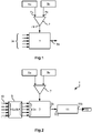
- Fig.1 represents a diagram of a serializer 3.
- the serializer 3 comprises a plurality of inputs 3a configured for receiving a plurality of incoming data signals corresponding to packet streams also called data bus. The different incoming data signals may have different throughputs or the same throughput.
- the serializer 3 also comprises an output 3b configured for transmitting a single outgoing data signal corresponding to a single stream of packets corresponding to the combination of the different incoming signals.
- the serializer 3 enables therefore to serializes a plurality of parallel bitstreams into a single bitstream having a bit rate corresponding to the sum of the bitrates of the parallel incoming bitstreams.
- a clock signal corresponding to the frequency (or symbol rate) of the outgoing signal has to be supplied to the serializer 3.
- Such clock signal is provided by an oscillator.
- a first reconfigurable oscillator 5a and a second reconfigurable oscillator 5b are used to supply a clock signal in order to enable a fast switching between the first oscillator 5a and the second oscillator 5b.
- the serializer 3 has to work at different frequencies depending on the demand so that a clock signal corresponding to the desired frequency has to be supplied to the serializer 3.
- a reconfigurable oscillator 5a, 5b is capable of providing clock signal at different frequencies but the reconfiguration time is generally very long with respect to the bitrate of the incoming signals so that a combination of two reconfigurable oscillators 5a and 5b needs to be used in order to reduce the time required for switching from a clock signal at a first frequency to a clock signal at a second frequency.
- a fast switching device 7 is used to enable the switching from the first reconfigurable oscillator 5a to the second reconfigurable oscillator 5b.
- the fast switching device 7 comprises a first input 7a linked to the first reconfigurable oscillator 5a, a second input 7b linked to the second reconfigurable oscillator 5b and an output 7d linked to the serializer 3.
- the fast switching device 7 is configured for linking one of the inputs 7a or 7b to the output 7d.
- the fast switching device 7 is also configured for switching, upon receipt of a frequency change signal, from a first switching state wherein the first input 7a is linked to the output 7d (the second input 7b is then not linked to the output 7d) to a second switching state wherein the second input 7b is linked to the output 7d (the first input 7a is then not linked to the output 7d) and inversely.
- the fast switching device 7 may be achieved with a field programmable gate array element, for example a Virtex ® -7 FPGA. However, any other fast switching element known in the state of the art and enabling a switching from the first switching state to the second switching state in a range of a nanosecond or a few ns may also be used.
- Fig.2 represents a transmitter 1 according to a first embodiment.
- the transmitter 1 comprises a serializer 3, a first 5a and a second 5b reconfigurable oscillators and a fast switching device 7 as described in Fig.1 .
- the transmitter 1 also comprises a buffer 9 comprising a plurality of inputs 9a configured for receiving and buffering the plurality of incoming data signals received by the transmitter 1. These incoming data signals correspond for example to a data bus 10 connected to the transmitter 1.
- the buffer 9 also comprises a plurality of outputs 9b linked respectively to the inputs of the serializer 3.
- the buffer 9 is configured for transmitting the buffered data signals to the serializer according to a predefined timing, each data signals being transmitted according to a predefined rate.
- the buffer 9 enables avoiding an interruption within a packet.
- the serializer3, the fast switching device 7 and the buffer 9 may be implemented on a common integrated circuit.
- the transmitter 3 may also comprise an electronic to optical converter 11.
- the electronic to optical converter 11 comprises an input 11a linked to the output 3b of the serializer 3 and an output 11b linked to an optical fiber 13.
- the electronic to optical converter is configured for converting the electronic data signal transmitted by the serializer 3 into an optical signal.
- the transmitter 1 is destined to be implemented into an ingress node of an optical network.
- the optical signal outputted by the electronic to optical converter 11 may then be transmitted toward a receiver of an egress node (not represented) via an optical link corresponding to the optical fiber 13.
- the transmitter 1 may be connected to a control plane unit (not represented) of the network configured for managing the data transmissions through the network.
- the control plane unit may be configured for transmitting a required frequency signal or a frequency change signal in order for the serializer 3 to be configured to produce an output signal at the required frequency signal.
- the control plane unit may be located in a central controller of the network which is remote from the transmitter 1.
- the first step 101 refers to the configuration of the transmitter 1 in order to transmit a data signal according to a first frequency produced by the first reconfigurable oscillator 5a so that the fast switching device 7 is in the first switching state.
- the second step 102 refers to the reception of a frequency change signal sent by a control plane unit to the transmitter 1 indicating that the data signal frequency has to be switched to a second frequency at a predefined time T1.
- the third step 103 corresponds to an estimation of the duration for switching from the first to the second frequency. This estimation may be achieved based on preliminary tests to determine the switching time for the frequencies associated to the possible transmitted signals. Such duration depends for example on the absolute value of the difference between the first and the second frequencies and on the time required by the serializer 3 to find a stable state in the second frequency. This estimated duration is then compared with a predetermined duration threshold. If the estimated duration is shorter than or equal to the predetermination duration threshold, the method goes to step 104 and if the estimated difference is higher than the predefined duration threshold, the method goes to step 104'.
- the predetermined duration may be chosen based on the buffer 9 capacity. Indeed, depending on the throughput of the transmitter 1, the buffer 9 capacity may allow to buffer the transmitted packets during a predetermined duration, for example 1ms. In such case, the predetermined duration is then chosen to be 1ms or less in order for the transmitter 1 to be able to switch from one frequency to the other during the maximum buffering time to ensure that no data packets are lost during the frequency switching.
- the fourth step 104 corresponds to the configuration of the second reconfigurable oscillator 5b at the second frequency.
- the fifth step 105 refers to the switching at the predefined time T1 of the fast switching device 1 to the second switching state and the configuration of the serializer 3 to transmit an output data signal at the second frequency.
- the switching is achieved during an interpacket gap, for example the next interpacket gap after the predefined time T1.
- the step 104' refers to the configuration of the second reconfigurable oscillator 5b to an intermediate frequency comprised in the range between the first and the second frequency, for example around half of the difference from the first and the second frequencies.
- the intermediate frequency is chosen among a standard set of frequencies in order to enable a stable configuration of the second reconfigurable oscillator 5b at the intermediate frequency.
- the standard frequency is for example chosen to be adapted to the receiver toward which the signal transmitted by the transmitter 1 is destined and to provide a stable state of the transmitter 1 that is reached in a time shorter than the predetermined duration threshold.
- the step 105' corresponds to the switching at the predefined time T1 of the fast switching device 7 to the second switching state and the configuration of the serializer 3 in order to transmit an output data signal at the intermediate frequency.
- the switching is achieved during an interpacket gap.
- the step 106' refers to the configuration of the first reconfigurable oscillator 5a at the second frequency.
- the step 107' refers to the switching at the predefined time T1 of the fast switching device 7 to the first switching state and the configuration of the serializer 3 to transmit an output data signal at the second frequency.
- the switching is achieved during an interpacket gap, for example the next interpacket gap after the predefined time T1.
- an intermediate frequency enables to switch from a first frequency to a second frequency without requiring a long reconfiguration due to the long stabilization of the serializer 3 due to the frequency difference.
- several intermediate frequencies can be used.
- Fig.4 represents a transmitter 1 according to a second embodiment.
- This embodiment differs from the first embodiment represented in fig.2 in that it comprises a third reconfigurable oscillator 5c and in that the fast switching device 7 comprises a third input 7c and a third switching state wherein the third input 7c is linked to the output 7d.
- the third input 7c being linked to the third reconfigurable oscillator 5c.
- the other elements of the transmitter 1 remains identical to the transmitter 1 of the first embodiment.
- the second reconfigurable oscillator 5b can be configured to transmit a signal at the intermediate frequency and the third reconfigurable oscillator 5c can be configured to transmit a signal at the second frequency.
- the fast switching device 7 is then switched successively from the first to the second switching state and from the second to the third switching state.
- the different switchings are for example launched by a frequency change signal sent by a control plane unit to the transmitter 1 indicating that the data signal frequency has to be switched to a second frequency at a predefined time T1.
- the switchings being achieved preferably during inter-packet gaps.
- the time lasts using the intermediate frequency may be as short as possible.
- Fig.5 represents a transmitter 1 according to a third embodiment.
- This embodiment differs from the first embodiment represented in fig.2 in that it comprises a digital to analog converter 15.
- the digital to analog converter 15 is implemented at the output of the serializer 3.
- the output of the digital to analog converter 15 is linked to the optical converter 11.
- the digital to analog converter 15 is configured for converting the digital signal provided by the serializer 3 into an analog signal.
- the digital to analog converter 15 is configured for using the same clock signal as the serializer 3.
- a second fast switching device 7' is therefore used for providing the clock signal providing by the first 5a or the second 5b reconfigurable oscillators to the digital to analog converter 15.
- the second fast switching device 7' has a first input 7'a linked to the first oscillator 5a, a second input 7'b linked to the second oscillator 5b and an output 7'd linked to the digital to analog converter 15.
- the second fast switching device 7' being configured for switching between a first switching state wherein its first input 7'a is linked to the output 7'd and a second switching state wherein its second input 7'b is linked to its output 7'd.
- the second fast switching device 7' is synchronized with the first fast switching device 7 so that the switchings from one switching state to the other are achieved simultaneously by both fast switching devices 7 and 7'.
- Both fast switching devices 7 and 7' can be implemented on a common integrated circuit.
- the integrated circuit may also comprise the buffer 9 and the serializer 3.
- the other elements of the transmitter 1 remains identical to the transmitter of the first embodiment.
- the digital to analog converter 15 enables to change the modulation format.
- the switching of frequency may correspond to a switching of modulation format.
- the digital to analog converter 15 is configured for converting digital levels in analog signals.
- the total number of digital levels depends on the capacity of the digital to analog converter 15, for example 32 levels for a 5-bit converter and the number of used levels may be adapted to the modulation format and the levels values may be adapted to the used modulation format.
- two digital to analog converters are used in parallel in order to process the two different polarizations of the signal.
- the data packets of the incoming data signals may be classified in different categories according to their importance.
- the serializer 3 may transmit packets belonging to selected categories.
- a frequency change signal is received by the transmitter 1 at a time T1
- Such time shift or de-synchronization may therefore lead to a loss of the packets notably if the frequency is switched to a lower frequency (corresponding to a lower throughput).
- the classification of the packets may then enable to avoid the loss of the most important packets.
- the present invention by the use of at least two reconfigurable oscillators 5a and 5b and at least one fast switching device 7, enables a hitless frequency switching wherein such frequency switching does not lead to an interruption of the traffic nor to a loss of data packets. Such features are particularly interesting for continuous data transmission in high throughput communication network.
- processors may be provided through the use of dedicated hardware as well as hardware capable of executing software in association with appropriate software.
- the functions may be provided by a single dedicated processor, by a single shared processor, or by a plurality of individual processors, some of which may be shared.
- explicit use of the term "processor” or “controller” should not be construed to refer exclusively to hardware capable of executing software, and may implicitly include, without limitation, digital signal processor (DSP) hardware, network processor, application specific integrated circuit (ASIC), field programmable gate array (FPGA), read only memory (ROM) for storing software, random access memory (RAM), and non volatile storage.
- DSP digital signal processor
- ASIC application specific integrated circuit
- FPGA field programmable gate array
- ROM read only memory
- RAM random access memory
- any switches shown in the FIGS. are conceptual only. Their function may be carried out through the operation of program logic, through dedicated logic, through the interaction of program control and dedicated logic, or even manually, the particular technique being selectable by the implementer as more specifically understood from the context.
Landscapes
- Engineering & Computer Science (AREA)
- Signal Processing (AREA)
- Computer Networks & Wireless Communication (AREA)
- Theoretical Computer Science (AREA)
- Computer Hardware Design (AREA)
- Communication Control (AREA)
- Transmitters (AREA)
Claims (12)
- Sender (1), umfassend:- einen Serialisierer (3) mit mehreren Eingängen (3a), ausgelegt zum Empfangen von ankommenden Datensignalen, die sukzessive Datenpakete umfassen, die mehreren Kanälen entsprechen, wobei der Serialisierer ausgelegt ist zum Serialisieren der ankommenden Datensignale in einem Ausgangssignal,
wobei der Sender (1) außerdem Folgendes umfasst:- einen ersten Oszillator (5a), ausgelegt zum Bereitstellen eines einer ersten Frequenz zugeordneten ersten Taktsignals für den Serialisierer (3),- einen zweiten Oszillator (5b), ausgelegt zum Bereitstellen eines einer von der ersten Frequenz verschiedenen zweiten Frequenz zugeordneten zweiten Taktsignals für den Serialisierer (3),- eine erste schnelle Schaltvorrichtung (7) mit einem mit dem ersten Oszillator (5a) verbundenen ersten Eingang (7a), einem mit dem zweiten Oszillator (5b) verbundenen zweiten Eingang (7b) und einem mit dem Serialisierer (3) verbundenen Ausgang (7d), wobei die erste schnelle Schaltvorrichtung (7) ausgelegt ist zum Umschalten zwischen einem ersten Schaltzustand, in dem der erste Eingang (7a) mit dem Ausgang (7d) verbunden ist, und einem zweiten Schaltzustand, in dem der zweite Eingang (7b) mit dem Ausgang (7d) verbunden ist,- einen Puffer (9), ausgelegt zum Puffern der mehreren ankommenden Datensignale,
dadurch gekennzeichnet, dass der Sender (1) dafür ausgelegt ist, bei Empfang eines Taktsignal-Änderungssignals die erste schnelle Schaltvorrichtung (7) während einer Lücke zwischen Paketen in den ankommenden Datenpaketen aus dem ersten in den zweiten Schaltzustand zu überführen. - Sender (1) nach Anspruch 1, umfassend:- einen Digital-Analog-Umsetzer (15), ausgelegt zum Umsetzen eines durch den Serialisierer (3) bereitgestellten Digitalsignals in ein Analogsignal unter Verwendung desselben Taktsignals wie der Serialisierer (3),- eine zweite schnelle Schaltvorrichtung (7') mit einem mit dem ersten Oszillator (5a) verbundenen ersten Eingang (7'a), einem mit dem zweiten Oszillator (5b) verbundenen zweiten Eingang (7'b) und einem mit dem Digital-Analog-Umsetzer (15) verbundenen Ausgang (7'd), wobei die zweite schnelle Schaltvorrichtung (7') ausgelegt ist zum Umschalten zwischen einem ersten Schaltzustand, in dem der erste Eingang (7'a) mit dem Ausgang (7'd) verbunden ist, und einem zweiten Schaltzustand, in dem der zweite Eingang (7'b) mit dem Ausgang (7'd) verbunden ist, wobei die zweite schnelle Schaltvorrichtung (7') mit der ersten schnellen Schaltvorrichtung (7) synchronisiert ist.
- Sender (1) nach Anspruch 2, wobei das Umschalten von einer ersten Übertragungsfrequenz auf eine zweite Übertragungsfrequenz einer Modulationsformatänderung entspricht.
- Sender (1) nach einem der vorhergehenden Ansprüche, der einen Elektronisch/Optisch-Umsetzer (11) umfasst, der dafür ausgelegt ist, das gesendete Signal umzusetzen und das umgesetzte Signal zu einer mit dem Sender (1) verbundenen optischen Faser (13) zu senden.
- Sender (1) nach einem der vorhergehenden Ansprüche, wobei sich der Puffer (9), der Serialisierer (3) und die mindestens eine schnelle Schaltvorrichtung (7, 7') auf einer gemeinsamen integrierten Schaltung befinden.
- Sender (1) nach einem der vorhergehenden Ansprüche, wobei das Umschalten von einer ersten auf eine zweite Übertragungsfrequenz einen Übergang über eine Zwischenfrequenz umfasst, wenn eine zum Umschalten von der ersten auf die zweite Frequenz erforderliche Zeit höher als eine vorbestimmte Dauerschwelle ist.
- Sender (1) nach einem der vorhergehenden Ansprüche, wobei die vorbestimmte Dauerschwelle auf der Basis der Kapazität des Puffers (9) bestimmt wird.
- Sender (1) nach Anspruch 6 oder 7, wobei die Zwischenfrequenz einer Frequenz im Bereich zwischen der ersten und der zweiten Frequenz entspricht.
- Sender (1) nach Anspruch 8, wobei die Zwischenfrequenz einer Standardfrequenz entspricht, die aus einer Menge von Frequenzen ausgewählt wird, die für einen Empfänger ausgelegt ist, für den das durch den Sender (1) gesendete Signal bestimmt ist, und dafür ausgelegt ist, einen stabilen Zustand des Senders (1) bereitzustellen, der in einer Zeit erreicht wird, die kürzer als die vorbestimmte Dauerschwelle ist.
- Sender (1) nach einem der vorhergehenden Ansprüche, wobei die Datenpakete der ankommenden Datensignale gemäß ihrer Wichtigkeit in verschiedene Kategorien eingeteilt werden und im Fall eines Umschaltens von einer ersten Frequenz auf eine zweite Frequenz, die niedriger als die erste Frequenz ist, und/oder einer Desynchronisation mit den ankommenden Datensignalen nur Pakete, die zu ausgewählten Kategorien gehören, durch den Serialisierer (3) gesendet werden.
- Verfahren zum Senden von Signalen mit verschiedenen Taktsignalen unter Verwendung eines Senders (1), umfassend:- einen Serialisierer (3) mit mehreren Eingängen (3a), ausgelegt zum Empfangen ankommender Datensignale, die von einem Ausgang eines Puffers (9) empfangen werden, die sukzessive Datenpakete umfassen, die mehreren Kanälen entsprechen, wobei der Serialisierer (3) ausgelegt ist zum Serialisieren der ankommenden Datensignale in einem Ausgangssignal,- einen ersten Oszillator (5a), ausgelegt zum Bereitstellen eines ersten Taktsignals für den Serialisierer (3),- einen zweiten Oszillator (5b), ausgelegt zum Bereitstellen eines zweiten Taktsignals für den Serialisierer (3),- eine erste schnelle Schaltvorrichtung (7) mit einem mit dem ersten Oszillator (5a) verbundenen ersten Eingang (7a), einem mit dem zweiten Oszillator (5b) verbundenen zweiten Eingang (7b) und einem mit dem Serialisierer (3) verbundenen Ausgang (7d), wobei die erste schnelle Schaltvorrichtung (7) ausgelegt ist zum Umschalten zwischen einem ersten Schaltzustand, in dem der erste Eingang (7a) mit dem Ausgang (7d) verbunden ist, und einem zweiten Schaltzustand, in dem der zweite Eingang (7b) mit dem Ausgang (7d) verbunden ist,
dadurch gekennzeichnet, dass das Verfahren die folgenden Schritte umfasst:- die erste schnelle Schaltvorrichtung (7) wird in den ersten Schaltzustand umgeschaltet,- der Serialisierer (3) wird angesteuert zur Serialisierung der ankommenden Datensignale mit einer ersten Übertragungsfrequenz unter Verwendung des durch den ersten Oszillator (5a) bereitgestellten ersten Taktsignals,im Fall einer Notwendigkeit, die Übertragungsfrequenz des Serialisierers (3) von der ersten Übertragungsfrequenz in eine von der ersten Frequenz verschiedene zweite Übertragungsfrequenz umzuändern,wenn die Differenz zwischen der ersten und zweiten Frequenz kleiner als eine vorbestimmte Schwelle ist,- wird der zweite Oszillator (5b) so eingestellt, dass das zweite Taktsignal der zweiten Übertragungsfrequenz entspricht, und- wird die erste schnelle Schaltvorrichtung (7) in den zweiten Schaltzustand umgeschaltet,- wird der Serialisierer (3) angesteuert zum Serialisieren der ankommenden Datensignale unter Verwendung des durch den zweiten Oszillator (5b) bereitgestellten zweiten Taktsignals,wenn die Differenz zwischen der ersten und zweiten Frequenz größer als eine vorbestimmte Schwelle ist,- wird der zweite Oszillator (5b) so eingestellt, dass das zweite Taktsignal einer Zwischenfrequenz in dem Bereich zwischen der ersten und der zweiten Frequenz entspricht,- wird die schnelle Schaltvorrichtung (7) in den zweiten Schaltzustand umgeschaltet,- wird der Serialisierer (3) angesteuert zum Serialisieren der ankommenden Datensignale unter Verwendung des durch den zweiten Oszillator (5b) bereitgestellten zweiten Taktsignals, das der Zwischenfrequenz entspricht,- wird der erste Oszillator (5a) so eingestellt, dass das erste Taktsignal der zweiten Frequenz entspricht,- wird die schnelle Schaltvorrichtung (7) in den ersten Schaltzustand umgeschaltet,- wird der Serialisierer (3) angesteuert zum Serialisieren der ankommenden Datensignale unter Verwendung des durch den ersten Oszillator (5a) bereitgestellten ersten Taktsignals, das der zweiten Frequenz entspricht,
und werden die Schritte des Umschaltens der schnellen Schaltvorrichtung (7) von dem ersten auf den zweiten Schaltzustand oder von dem zweiten auf den ersten Schaltzustand während einer Lücke zwischen Paketen der ankommenden Datensignale in dem Serialisierer (3) erzielt. - Verfahren nach Anspruch 11, wobei der Sender (1) außerdem Folgendes umfasst:- einen Digital-Analog-Umsetzer (15), der mit dem Ausgang des Serialisierers (3) verbunden ist,- eine zweite schnelle Schaltvorrichtung (7') mit einem mit dem ersten Oszillator (5a) verbundenen ersten Eingang (7'a), einem mit dem zweiten Oszillator (5b) verbundenen zweiten Eingang (7'b) und einem mit dem Digital-Analog-Umsetzer (15) verbundenen Ausgang (7'd), wobei die zweite schnelle Schaltvorrichtung (7') ausgelegt ist zum Umschalten zwischen einem ersten Schaltzustand, in dem der erste Eingang (7'a) mit dem Ausgang (7'd) verbunden ist, und einem zweiten Schaltzustand, in dem der zweite Eingang (7'b) mit dem Ausgang (7'd) verbunden ist, wobei die zweite schnelle Schaltvorrichtung (7') mit der ersten schnellen Schaltvorrichtung (7) synchronisiert ist, zum Umschalten von einem Schaltzustand auf den anderen.
Priority Applications (1)
| Application Number | Priority Date | Filing Date | Title |
|---|---|---|---|
| EP17305449.5A EP3389202B1 (de) | 2017-04-14 | 2017-04-14 | Mehrfrequenz-sender und zugehöriges verfahren |
Applications Claiming Priority (1)
| Application Number | Priority Date | Filing Date | Title |
|---|---|---|---|
| EP17305449.5A EP3389202B1 (de) | 2017-04-14 | 2017-04-14 | Mehrfrequenz-sender und zugehöriges verfahren |
Publications (2)
| Publication Number | Publication Date |
|---|---|
| EP3389202A1 EP3389202A1 (de) | 2018-10-17 |
| EP3389202B1 true EP3389202B1 (de) | 2022-10-05 |
Family
ID=58664623
Family Applications (1)
| Application Number | Title | Priority Date | Filing Date |
|---|---|---|---|
| EP17305449.5A Active EP3389202B1 (de) | 2017-04-14 | 2017-04-14 | Mehrfrequenz-sender und zugehöriges verfahren |
Country Status (1)
| Country | Link |
|---|---|
| EP (1) | EP3389202B1 (de) |
Family Cites Families (4)
| Publication number | Priority date | Publication date | Assignee | Title |
|---|---|---|---|---|
| US4849970A (en) * | 1988-05-19 | 1989-07-18 | Advanced Micro Devices, Inc. | Smoothing apparatus for an independently clocked network |
| US20050066045A1 (en) * | 2003-09-03 | 2005-03-24 | Johnson Neil James | Integrated network interface supporting multiple data transfer protocols |
| JP2005339323A (ja) * | 2004-05-28 | 2005-12-08 | Hitachi Ltd | ストレージシステム、計算機システムおよびインタフェースモジュール |
| US7467319B1 (en) * | 2004-08-27 | 2008-12-16 | Xilinx, Inc. | Ethernet media access controller embedded in a programmable logic device—clock interface |
-
2017
- 2017-04-14 EP EP17305449.5A patent/EP3389202B1/de active Active
Also Published As
| Publication number | Publication date |
|---|---|
| EP3389202A1 (de) | 2018-10-17 |
Similar Documents
| Publication | Publication Date | Title |
|---|---|---|
| EP2683102B1 (de) | Vorrichtung und Verfahren zur Übertragung von Proben eines digitalen Basisbandsignals | |
| US10298380B2 (en) | Method for transmitting data in a communication network of an industrial automation system and coupling communication device | |
| EP1965601B1 (de) | System und Verfahren zur optischen Übertragung | |
| US9634950B2 (en) | Ethernet media converter supporting high-speed wireless access points | |
| US7710992B2 (en) | Communication device and communication method | |
| EP3264725A1 (de) | Umwandler der stream-reservierungsklasse | |
| JP2006262478A (ja) | 光ネットワーク及びノード | |
| EP2262139A1 (de) | Variables Bitratengerät | |
| CN109151830B (zh) | 一种频谱整理的方法、装置、设备和系统 | |
| US20150063516A1 (en) | Communication circuit and information processing device | |
| US20230044462A1 (en) | Low Latency Network Device and Method for Treating Received Serial Data | |
| EP3389202B1 (de) | Mehrfrequenz-sender und zugehöriges verfahren | |
| TWI555358B (zh) | Communication frame transfer device and communication system | |
| US9912493B2 (en) | Home network signal relay device in access network and home network signal relay method in access network using same | |
| KR100630131B1 (ko) | 무선 근거리 네트워크에서 방송 서비스의 서비스 품질을보장하는 엑세스 포인트 장치 | |
| US8892793B1 (en) | Techniques for oversampling a data stream in an integrated circuit | |
| US10911986B2 (en) | Wireless communication device, wireless communication system, and wireless communication method | |
| CN102811168B (zh) | 同步网络交换机 | |
| JP2019176289A (ja) | 無線通信装置、無線通信システムおよび無線通信方法 | |
| EP2015484A1 (de) | Verfahren zur Datenübertragung und entsprechendes Sende-/Empfangsgerät | |
| KR100457869B1 (ko) | 파장분할다중 링 네트워크에 적용되는 멀티 홉 임베딩방식의 노드간 패킷 전송방법 | |
| EP1936881A1 (de) | Überwachung von durch Paketverzögerungsveränderung induziertem Abgleiten in einem TDM-über-Ethernet-Übertragungsnetzwerk | |
| JP3581112B2 (ja) | データ送信方法および送信回路並びに通信機器 | |
| JP2007074419A (ja) | データ分割装置、データ結合装置、送受信システム、データ分割方法、およびデータ結合方法 | |
| US20150172008A1 (en) | Wireless transfer device and method for control of wireless transfer band |
Legal Events
| Date | Code | Title | Description |
|---|---|---|---|
| PUAI | Public reference made under article 153(3) epc to a published international application that has entered the european phase |
Free format text: ORIGINAL CODE: 0009012 |
|
| STAA | Information on the status of an ep patent application or granted ep patent |
Free format text: STATUS: REQUEST FOR EXAMINATION WAS MADE |
|
| 17P | Request for examination filed |
Effective date: 20171215 |
|
| AK | Designated contracting states |
Kind code of ref document: A1 Designated state(s): AL AT BE BG CH CY CZ DE DK EE ES FI FR GB GR HR HU IE IS IT LI LT LU LV MC MK MT NL NO PL PT RO RS SE SI SK SM TR |
|
| AX | Request for extension of the european patent |
Extension state: BA ME |
|
| RBV | Designated contracting states (corrected) |
Designated state(s): AL AT BE BG CH CY CZ DE DK EE ES FI FR GB GR HR HU IE IS IT LI LT LU LV MC MK MT NL NO PL PT RO RS SE SI SK SM TR |
|
| RAP1 | Party data changed (applicant data changed or rights of an application transferred) |
Owner name: NOKIA SOLUTIONS AND NETWORKS OY |
|
| STAA | Information on the status of an ep patent application or granted ep patent |
Free format text: STATUS: EXAMINATION IS IN PROGRESS |
|
| 17Q | First examination report despatched |
Effective date: 20210629 |
|
| GRAP | Despatch of communication of intention to grant a patent |
Free format text: ORIGINAL CODE: EPIDOSNIGR1 |
|
| STAA | Information on the status of an ep patent application or granted ep patent |
Free format text: STATUS: GRANT OF PATENT IS INTENDED |
|
| INTG | Intention to grant announced |
Effective date: 20220502 |
|
| GRAS | Grant fee paid |
Free format text: ORIGINAL CODE: EPIDOSNIGR3 |
|
| GRAA | (expected) grant |
Free format text: ORIGINAL CODE: 0009210 |
|
| STAA | Information on the status of an ep patent application or granted ep patent |
Free format text: STATUS: THE PATENT HAS BEEN GRANTED |
|
| AK | Designated contracting states |
Kind code of ref document: B1 Designated state(s): AL AT BE BG CH CY CZ DE DK EE ES FI FR GB GR HR HU IE IS IT LI LT LU LV MC MK MT NL NO PL PT RO RS SE SI SK SM TR |
|
| REG | Reference to a national code |
Ref country code: GB Ref legal event code: FG4D |
|
| REG | Reference to a national code |
Ref country code: CH Ref legal event code: EP |
|
| REG | Reference to a national code |
Ref country code: AT Ref legal event code: REF Ref document number: 1523416 Country of ref document: AT Kind code of ref document: T Effective date: 20221015 |
|
| REG | Reference to a national code |
Ref country code: IE Ref legal event code: FG4D |
|
| REG | Reference to a national code |
Ref country code: DE Ref legal event code: R096 Ref document number: 602017062340 Country of ref document: DE |
|
| REG | Reference to a national code |
Ref country code: LT Ref legal event code: MG9D |
|
| REG | Reference to a national code |
Ref country code: NL Ref legal event code: MP Effective date: 20221005 |
|
| REG | Reference to a national code |
Ref country code: AT Ref legal event code: MK05 Ref document number: 1523416 Country of ref document: AT Kind code of ref document: T Effective date: 20221005 |
|
| PG25 | Lapsed in a contracting state [announced via postgrant information from national office to epo] |
Ref country code: NL Free format text: LAPSE BECAUSE OF FAILURE TO SUBMIT A TRANSLATION OF THE DESCRIPTION OR TO PAY THE FEE WITHIN THE PRESCRIBED TIME-LIMIT Effective date: 20221005 |
|
| PG25 | Lapsed in a contracting state [announced via postgrant information from national office to epo] |
Ref country code: SE Free format text: LAPSE BECAUSE OF FAILURE TO SUBMIT A TRANSLATION OF THE DESCRIPTION OR TO PAY THE FEE WITHIN THE PRESCRIBED TIME-LIMIT Effective date: 20221005 Ref country code: PT Free format text: LAPSE BECAUSE OF FAILURE TO SUBMIT A TRANSLATION OF THE DESCRIPTION OR TO PAY THE FEE WITHIN THE PRESCRIBED TIME-LIMIT Effective date: 20230206 Ref country code: NO Free format text: LAPSE BECAUSE OF FAILURE TO SUBMIT A TRANSLATION OF THE DESCRIPTION OR TO PAY THE FEE WITHIN THE PRESCRIBED TIME-LIMIT Effective date: 20230105 Ref country code: LT Free format text: LAPSE BECAUSE OF FAILURE TO SUBMIT A TRANSLATION OF THE DESCRIPTION OR TO PAY THE FEE WITHIN THE PRESCRIBED TIME-LIMIT Effective date: 20221005 Ref country code: FI Free format text: LAPSE BECAUSE OF FAILURE TO SUBMIT A TRANSLATION OF THE DESCRIPTION OR TO PAY THE FEE WITHIN THE PRESCRIBED TIME-LIMIT Effective date: 20221005 Ref country code: ES Free format text: LAPSE BECAUSE OF FAILURE TO SUBMIT A TRANSLATION OF THE DESCRIPTION OR TO PAY THE FEE WITHIN THE PRESCRIBED TIME-LIMIT Effective date: 20221005 Ref country code: AT Free format text: LAPSE BECAUSE OF FAILURE TO SUBMIT A TRANSLATION OF THE DESCRIPTION OR TO PAY THE FEE WITHIN THE PRESCRIBED TIME-LIMIT Effective date: 20221005 |
|
| PG25 | Lapsed in a contracting state [announced via postgrant information from national office to epo] |
Ref country code: RS Free format text: LAPSE BECAUSE OF FAILURE TO SUBMIT A TRANSLATION OF THE DESCRIPTION OR TO PAY THE FEE WITHIN THE PRESCRIBED TIME-LIMIT Effective date: 20221005 Ref country code: PL Free format text: LAPSE BECAUSE OF FAILURE TO SUBMIT A TRANSLATION OF THE DESCRIPTION OR TO PAY THE FEE WITHIN THE PRESCRIBED TIME-LIMIT Effective date: 20221005 Ref country code: LV Free format text: LAPSE BECAUSE OF FAILURE TO SUBMIT A TRANSLATION OF THE DESCRIPTION OR TO PAY THE FEE WITHIN THE PRESCRIBED TIME-LIMIT Effective date: 20221005 Ref country code: IS Free format text: LAPSE BECAUSE OF FAILURE TO SUBMIT A TRANSLATION OF THE DESCRIPTION OR TO PAY THE FEE WITHIN THE PRESCRIBED TIME-LIMIT Effective date: 20230205 Ref country code: HR Free format text: LAPSE BECAUSE OF FAILURE TO SUBMIT A TRANSLATION OF THE DESCRIPTION OR TO PAY THE FEE WITHIN THE PRESCRIBED TIME-LIMIT Effective date: 20221005 Ref country code: GR Free format text: LAPSE BECAUSE OF FAILURE TO SUBMIT A TRANSLATION OF THE DESCRIPTION OR TO PAY THE FEE WITHIN THE PRESCRIBED TIME-LIMIT Effective date: 20230106 |
|
| REG | Reference to a national code |
Ref country code: DE Ref legal event code: R097 Ref document number: 602017062340 Country of ref document: DE |
|
| PG25 | Lapsed in a contracting state [announced via postgrant information from national office to epo] |
Ref country code: SM Free format text: LAPSE BECAUSE OF FAILURE TO SUBMIT A TRANSLATION OF THE DESCRIPTION OR TO PAY THE FEE WITHIN THE PRESCRIBED TIME-LIMIT Effective date: 20221005 Ref country code: RO Free format text: LAPSE BECAUSE OF FAILURE TO SUBMIT A TRANSLATION OF THE DESCRIPTION OR TO PAY THE FEE WITHIN THE PRESCRIBED TIME-LIMIT Effective date: 20221005 Ref country code: EE Free format text: LAPSE BECAUSE OF FAILURE TO SUBMIT A TRANSLATION OF THE DESCRIPTION OR TO PAY THE FEE WITHIN THE PRESCRIBED TIME-LIMIT Effective date: 20221005 Ref country code: DK Free format text: LAPSE BECAUSE OF FAILURE TO SUBMIT A TRANSLATION OF THE DESCRIPTION OR TO PAY THE FEE WITHIN THE PRESCRIBED TIME-LIMIT Effective date: 20221005 Ref country code: CZ Free format text: LAPSE BECAUSE OF FAILURE TO SUBMIT A TRANSLATION OF THE DESCRIPTION OR TO PAY THE FEE WITHIN THE PRESCRIBED TIME-LIMIT Effective date: 20221005 |
|
| PLBE | No opposition filed within time limit |
Free format text: ORIGINAL CODE: 0009261 |
|
| STAA | Information on the status of an ep patent application or granted ep patent |
Free format text: STATUS: NO OPPOSITION FILED WITHIN TIME LIMIT |
|
| PG25 | Lapsed in a contracting state [announced via postgrant information from national office to epo] |
Ref country code: SK Free format text: LAPSE BECAUSE OF FAILURE TO SUBMIT A TRANSLATION OF THE DESCRIPTION OR TO PAY THE FEE WITHIN THE PRESCRIBED TIME-LIMIT Effective date: 20221005 Ref country code: AL Free format text: LAPSE BECAUSE OF FAILURE TO SUBMIT A TRANSLATION OF THE DESCRIPTION OR TO PAY THE FEE WITHIN THE PRESCRIBED TIME-LIMIT Effective date: 20221005 |
|
| 26N | No opposition filed |
Effective date: 20230706 |
|
| PG25 | Lapsed in a contracting state [announced via postgrant information from national office to epo] |
Ref country code: SI Free format text: LAPSE BECAUSE OF FAILURE TO SUBMIT A TRANSLATION OF THE DESCRIPTION OR TO PAY THE FEE WITHIN THE PRESCRIBED TIME-LIMIT Effective date: 20221005 |
|
| REG | Reference to a national code |
Ref country code: CH Ref legal event code: PL |
|
| PG25 | Lapsed in a contracting state [announced via postgrant information from national office to epo] |
Ref country code: LU Free format text: LAPSE BECAUSE OF NON-PAYMENT OF DUE FEES Effective date: 20230414 |
|
| REG | Reference to a national code |
Ref country code: BE Ref legal event code: MM Effective date: 20230430 |
|
| PG25 | Lapsed in a contracting state [announced via postgrant information from national office to epo] |
Ref country code: MC Free format text: LAPSE BECAUSE OF FAILURE TO SUBMIT A TRANSLATION OF THE DESCRIPTION OR TO PAY THE FEE WITHIN THE PRESCRIBED TIME-LIMIT Effective date: 20221005 |
|
| PG25 | Lapsed in a contracting state [announced via postgrant information from national office to epo] |
Ref country code: MC Free format text: LAPSE BECAUSE OF FAILURE TO SUBMIT A TRANSLATION OF THE DESCRIPTION OR TO PAY THE FEE WITHIN THE PRESCRIBED TIME-LIMIT Effective date: 20221005 Ref country code: LI Free format text: LAPSE BECAUSE OF NON-PAYMENT OF DUE FEES Effective date: 20230430 Ref country code: FR Free format text: LAPSE BECAUSE OF NON-PAYMENT OF DUE FEES Effective date: 20230430 Ref country code: CH Free format text: LAPSE BECAUSE OF NON-PAYMENT OF DUE FEES Effective date: 20230430 |
|
| REG | Reference to a national code |
Ref country code: IE Ref legal event code: MM4A |
|
| PG25 | Lapsed in a contracting state [announced via postgrant information from national office to epo] |
Ref country code: BE Free format text: LAPSE BECAUSE OF NON-PAYMENT OF DUE FEES Effective date: 20230430 |
|
| PG25 | Lapsed in a contracting state [announced via postgrant information from national office to epo] |
Ref country code: IE Free format text: LAPSE BECAUSE OF NON-PAYMENT OF DUE FEES Effective date: 20230414 |
|
| PG25 | Lapsed in a contracting state [announced via postgrant information from national office to epo] |
Ref country code: IE Free format text: LAPSE BECAUSE OF NON-PAYMENT OF DUE FEES Effective date: 20230414 |
|
| PGFP | Annual fee paid to national office [announced via postgrant information from national office to epo] |
Ref country code: GB Payment date: 20240229 Year of fee payment: 8 |
|
| PG25 | Lapsed in a contracting state [announced via postgrant information from national office to epo] |
Ref country code: IT Free format text: LAPSE BECAUSE OF FAILURE TO SUBMIT A TRANSLATION OF THE DESCRIPTION OR TO PAY THE FEE WITHIN THE PRESCRIBED TIME-LIMIT Effective date: 20221005 |
|
| PGFP | Annual fee paid to national office [announced via postgrant information from national office to epo] |
Ref country code: DE Payment date: 20240306 Year of fee payment: 8 |
|
| PG25 | Lapsed in a contracting state [announced via postgrant information from national office to epo] |
Ref country code: BG Free format text: LAPSE BECAUSE OF FAILURE TO SUBMIT A TRANSLATION OF THE DESCRIPTION OR TO PAY THE FEE WITHIN THE PRESCRIBED TIME-LIMIT Effective date: 20221005 |
|
| PG25 | Lapsed in a contracting state [announced via postgrant information from national office to epo] |
Ref country code: BG Free format text: LAPSE BECAUSE OF FAILURE TO SUBMIT A TRANSLATION OF THE DESCRIPTION OR TO PAY THE FEE WITHIN THE PRESCRIBED TIME-LIMIT Effective date: 20221005 |
|
| PG25 | Lapsed in a contracting state [announced via postgrant information from national office to epo] |
Ref country code: CY Free format text: LAPSE BECAUSE OF FAILURE TO SUBMIT A TRANSLATION OF THE DESCRIPTION OR TO PAY THE FEE WITHIN THE PRESCRIBED TIME-LIMIT; INVALID AB INITIO Effective date: 20170414 |
|
| PG25 | Lapsed in a contracting state [announced via postgrant information from national office to epo] |
Ref country code: HU Free format text: LAPSE BECAUSE OF FAILURE TO SUBMIT A TRANSLATION OF THE DESCRIPTION OR TO PAY THE FEE WITHIN THE PRESCRIBED TIME-LIMIT; INVALID AB INITIO Effective date: 20170414 |
|
| REG | Reference to a national code |
Ref country code: DE Ref legal event code: R119 Ref document number: 602017062340 Country of ref document: DE |
|
| PG25 | Lapsed in a contracting state [announced via postgrant information from national office to epo] |
Ref country code: TR Free format text: LAPSE BECAUSE OF FAILURE TO SUBMIT A TRANSLATION OF THE DESCRIPTION OR TO PAY THE FEE WITHIN THE PRESCRIBED TIME-LIMIT Effective date: 20221005 |
|
| GBPC | Gb: european patent ceased through non-payment of renewal fee |
Effective date: 20250414 |
|
| PG25 | Lapsed in a contracting state [announced via postgrant information from national office to epo] |
Ref country code: DE Free format text: LAPSE BECAUSE OF NON-PAYMENT OF DUE FEES Effective date: 20251104 |
|
| PG25 | Lapsed in a contracting state [announced via postgrant information from national office to epo] |
Ref country code: GB Free format text: LAPSE BECAUSE OF NON-PAYMENT OF DUE FEES Effective date: 20250414 |