EP3385981A1 - Appareil d'alimentation - Google Patents
Appareil d'alimentation Download PDFInfo
- Publication number
- EP3385981A1 EP3385981A1 EP17164854.6A EP17164854A EP3385981A1 EP 3385981 A1 EP3385981 A1 EP 3385981A1 EP 17164854 A EP17164854 A EP 17164854A EP 3385981 A1 EP3385981 A1 EP 3385981A1
- Authority
- EP
- European Patent Office
- Prior art keywords
- transistor
- source
- drain
- gate
- conductive
- Prior art date
- Legal status (The legal status is an assumption and is not a legal conclusion. Google has not performed a legal analysis and makes no representation as to the accuracy of the status listed.)
- Pending
Links
- 239000004020 conductor Substances 0.000 claims abstract description 15
- 239000000758 substrate Substances 0.000 claims description 10
- 238000000034 method Methods 0.000 claims description 7
- 238000013459 approach Methods 0.000 description 10
- 238000004519 manufacturing process Methods 0.000 description 6
- 238000005516 engineering process Methods 0.000 description 4
- 238000012986 modification Methods 0.000 description 4
- 230000004048 modification Effects 0.000 description 4
- 238000006243 chemical reaction Methods 0.000 description 2
- 239000003989 dielectric material Substances 0.000 description 2
- 230000000694 effects Effects 0.000 description 2
- 239000000463 material Substances 0.000 description 2
- 230000009467 reduction Effects 0.000 description 2
- 239000004065 semiconductor Substances 0.000 description 2
- 230000009286 beneficial effect Effects 0.000 description 1
- 238000004891 communication Methods 0.000 description 1
- 238000001816 cooling Methods 0.000 description 1
- 238000010586 diagram Methods 0.000 description 1
- 238000007667 floating Methods 0.000 description 1
- 238000000465 moulding Methods 0.000 description 1
- 230000000717 retained effect Effects 0.000 description 1
- 239000007787 solid Substances 0.000 description 1
Images


Classifications
-
- H—ELECTRICITY
- H01—ELECTRIC ELEMENTS
- H01L—SEMICONDUCTOR DEVICES NOT COVERED BY CLASS H10
- H01L23/00—Details of semiconductor or other solid state devices
- H01L23/48—Arrangements for conducting electric current to or from the solid state body in operation, e.g. leads, terminal arrangements ; Selection of materials therefor
- H01L23/488—Arrangements for conducting electric current to or from the solid state body in operation, e.g. leads, terminal arrangements ; Selection of materials therefor consisting of soldered or bonded constructions
- H01L23/495—Lead-frames or other flat leads
- H01L23/49575—Assemblies of semiconductor devices on lead frames
-
- H—ELECTRICITY
- H01—ELECTRIC ELEMENTS
- H01L—SEMICONDUCTOR DEVICES NOT COVERED BY CLASS H10
- H01L25/00—Assemblies consisting of a plurality of semiconductor or other solid state devices
- H01L25/18—Assemblies consisting of a plurality of semiconductor or other solid state devices the devices being of the types provided for in two or more different main groups of the same subclass of H10B, H10D, H10F, H10H, H10K or H10N
-
- H—ELECTRICITY
- H01—ELECTRIC ELEMENTS
- H01L—SEMICONDUCTOR DEVICES NOT COVERED BY CLASS H10
- H01L21/00—Processes or apparatus adapted for the manufacture or treatment of semiconductor or solid state devices or of parts thereof
- H01L21/02—Manufacture or treatment of semiconductor devices or of parts thereof
- H01L21/04—Manufacture or treatment of semiconductor devices or of parts thereof the devices having potential barriers, e.g. a PN junction, depletion layer or carrier concentration layer
- H01L21/48—Manufacture or treatment of parts, e.g. containers, prior to assembly of the devices, using processes not provided for in a single one of the groups H01L21/18 - H01L21/326 or H10D48/04 - H10D48/07
- H01L21/4814—Conductive parts
- H01L21/4821—Flat leads, e.g. lead frames with or without insulating supports
- H01L21/4825—Connection or disconnection of other leads to or from flat leads, e.g. wires, bumps, other flat leads
-
- H—ELECTRICITY
- H01—ELECTRIC ELEMENTS
- H01L—SEMICONDUCTOR DEVICES NOT COVERED BY CLASS H10
- H01L23/00—Details of semiconductor or other solid state devices
- H01L23/48—Arrangements for conducting electric current to or from the solid state body in operation, e.g. leads, terminal arrangements ; Selection of materials therefor
- H01L23/488—Arrangements for conducting electric current to or from the solid state body in operation, e.g. leads, terminal arrangements ; Selection of materials therefor consisting of soldered or bonded constructions
- H01L23/495—Lead-frames or other flat leads
- H01L23/49503—Lead-frames or other flat leads characterised by the die pad
-
- H—ELECTRICITY
- H01—ELECTRIC ELEMENTS
- H01L—SEMICONDUCTOR DEVICES NOT COVERED BY CLASS H10
- H01L23/00—Details of semiconductor or other solid state devices
- H01L23/48—Arrangements for conducting electric current to or from the solid state body in operation, e.g. leads, terminal arrangements ; Selection of materials therefor
- H01L23/488—Arrangements for conducting electric current to or from the solid state body in operation, e.g. leads, terminal arrangements ; Selection of materials therefor consisting of soldered or bonded constructions
- H01L23/495—Lead-frames or other flat leads
- H01L23/49517—Additional leads
- H01L23/4952—Additional leads the additional leads being a bump or a wire
-
- H—ELECTRICITY
- H01—ELECTRIC ELEMENTS
- H01L—SEMICONDUCTOR DEVICES NOT COVERED BY CLASS H10
- H01L23/00—Details of semiconductor or other solid state devices
- H01L23/48—Arrangements for conducting electric current to or from the solid state body in operation, e.g. leads, terminal arrangements ; Selection of materials therefor
- H01L23/488—Arrangements for conducting electric current to or from the solid state body in operation, e.g. leads, terminal arrangements ; Selection of materials therefor consisting of soldered or bonded constructions
- H01L23/495—Lead-frames or other flat leads
- H01L23/49517—Additional leads
- H01L23/49524—Additional leads the additional leads being a tape carrier or flat leads
-
- H—ELECTRICITY
- H01—ELECTRIC ELEMENTS
- H01L—SEMICONDUCTOR DEVICES NOT COVERED BY CLASS H10
- H01L23/00—Details of semiconductor or other solid state devices
- H01L23/48—Arrangements for conducting electric current to or from the solid state body in operation, e.g. leads, terminal arrangements ; Selection of materials therefor
- H01L23/488—Arrangements for conducting electric current to or from the solid state body in operation, e.g. leads, terminal arrangements ; Selection of materials therefor consisting of soldered or bonded constructions
- H01L23/495—Lead-frames or other flat leads
- H01L23/49541—Geometry of the lead-frame
- H01L23/49562—Geometry of the lead-frame for individual devices of subclass H10D
-
- H—ELECTRICITY
- H01—ELECTRIC ELEMENTS
- H01L—SEMICONDUCTOR DEVICES NOT COVERED BY CLASS H10
- H01L24/00—Arrangements for connecting or disconnecting semiconductor or solid-state bodies; Methods or apparatus related thereto
- H01L24/01—Means for bonding being attached to, or being formed on, the surface to be connected, e.g. chip-to-package, die-attach, "first-level" interconnects; Manufacturing methods related thereto
- H01L24/34—Strap connectors, e.g. copper straps for grounding power devices; Manufacturing methods related thereto
- H01L24/39—Structure, shape, material or disposition of the strap connectors after the connecting process
- H01L24/40—Structure, shape, material or disposition of the strap connectors after the connecting process of an individual strap connector
-
- H—ELECTRICITY
- H01—ELECTRIC ELEMENTS
- H01L—SEMICONDUCTOR DEVICES NOT COVERED BY CLASS H10
- H01L24/00—Arrangements for connecting or disconnecting semiconductor or solid-state bodies; Methods or apparatus related thereto
- H01L24/01—Means for bonding being attached to, or being formed on, the surface to be connected, e.g. chip-to-package, die-attach, "first-level" interconnects; Manufacturing methods related thereto
- H01L24/42—Wire connectors; Manufacturing methods related thereto
- H01L24/47—Structure, shape, material or disposition of the wire connectors after the connecting process
- H01L24/48—Structure, shape, material or disposition of the wire connectors after the connecting process of an individual wire connector
-
- H—ELECTRICITY
- H03—ELECTRONIC CIRCUITRY
- H03K—PULSE TECHNIQUE
- H03K17/00—Electronic switching or gating, i.e. not by contact-making and –breaking
- H03K17/51—Electronic switching or gating, i.e. not by contact-making and –breaking characterised by the components used
- H03K17/56—Electronic switching or gating, i.e. not by contact-making and –breaking characterised by the components used by the use, as active elements, of semiconductor devices
- H03K17/687—Electronic switching or gating, i.e. not by contact-making and –breaking characterised by the components used by the use, as active elements, of semiconductor devices the devices being field-effect transistors
-
- H—ELECTRICITY
- H01—ELECTRIC ELEMENTS
- H01L—SEMICONDUCTOR DEVICES NOT COVERED BY CLASS H10
- H01L2224/00—Indexing scheme for arrangements for connecting or disconnecting semiconductor or solid-state bodies and methods related thereto as covered by H01L24/00
- H01L2224/01—Means for bonding being attached to, or being formed on, the surface to be connected, e.g. chip-to-package, die-attach, "first-level" interconnects; Manufacturing methods related thereto
- H01L2224/34—Strap connectors, e.g. copper straps for grounding power devices; Manufacturing methods related thereto
- H01L2224/39—Structure, shape, material or disposition of the strap connectors after the connecting process
- H01L2224/40—Structure, shape, material or disposition of the strap connectors after the connecting process of an individual strap connector
- H01L2224/401—Disposition
- H01L2224/40135—Connecting between different semiconductor or solid-state bodies, i.e. chip-to-chip
- H01L2224/40137—Connecting between different semiconductor or solid-state bodies, i.e. chip-to-chip the bodies being arranged next to each other, e.g. on a common substrate
-
- H—ELECTRICITY
- H01—ELECTRIC ELEMENTS
- H01L—SEMICONDUCTOR DEVICES NOT COVERED BY CLASS H10
- H01L2224/00—Indexing scheme for arrangements for connecting or disconnecting semiconductor or solid-state bodies and methods related thereto as covered by H01L24/00
- H01L2224/01—Means for bonding being attached to, or being formed on, the surface to be connected, e.g. chip-to-package, die-attach, "first-level" interconnects; Manufacturing methods related thereto
- H01L2224/42—Wire connectors; Manufacturing methods related thereto
- H01L2224/47—Structure, shape, material or disposition of the wire connectors after the connecting process
- H01L2224/48—Structure, shape, material or disposition of the wire connectors after the connecting process of an individual wire connector
- H01L2224/481—Disposition
- H01L2224/48151—Connecting between a semiconductor or solid-state body and an item not being a semiconductor or solid-state body, e.g. chip-to-substrate, chip-to-passive
- H01L2224/48221—Connecting between a semiconductor or solid-state body and an item not being a semiconductor or solid-state body, e.g. chip-to-substrate, chip-to-passive the body and the item being stacked
- H01L2224/48245—Connecting between a semiconductor or solid-state body and an item not being a semiconductor or solid-state body, e.g. chip-to-substrate, chip-to-passive the body and the item being stacked the item being metallic
-
- H—ELECTRICITY
- H01—ELECTRIC ELEMENTS
- H01L—SEMICONDUCTOR DEVICES NOT COVERED BY CLASS H10
- H01L2224/00—Indexing scheme for arrangements for connecting or disconnecting semiconductor or solid-state bodies and methods related thereto as covered by H01L24/00
- H01L2224/73—Means for bonding being of different types provided for in two or more of groups H01L2224/10, H01L2224/18, H01L2224/26, H01L2224/34, H01L2224/42, H01L2224/50, H01L2224/63, H01L2224/71
- H01L2224/732—Location after the connecting process
- H01L2224/73201—Location after the connecting process on the same surface
- H01L2224/73221—Strap and wire connectors
-
- H—ELECTRICITY
- H01—ELECTRIC ELEMENTS
- H01L—SEMICONDUCTOR DEVICES NOT COVERED BY CLASS H10
- H01L24/00—Arrangements for connecting or disconnecting semiconductor or solid-state bodies; Methods or apparatus related thereto
- H01L24/71—Means for bonding not being attached to, or not being formed on, the surface to be connected
- H01L24/72—Detachable connecting means consisting of mechanical auxiliary parts connecting the device, e.g. pressure contacts using springs or clips
-
- H—ELECTRICITY
- H01—ELECTRIC ELEMENTS
- H01L—SEMICONDUCTOR DEVICES NOT COVERED BY CLASS H10
- H01L24/00—Arrangements for connecting or disconnecting semiconductor or solid-state bodies; Methods or apparatus related thereto
- H01L24/90—Methods for connecting semiconductor or solid state bodies using means for bonding not being attached to, or not being formed on, the body surface to be connected, e.g. pressure contacts using springs or clips
-
- H—ELECTRICITY
- H01—ELECTRIC ELEMENTS
- H01L—SEMICONDUCTOR DEVICES NOT COVERED BY CLASS H10
- H01L2924/00—Indexing scheme for arrangements or methods for connecting or disconnecting semiconductor or solid-state bodies as covered by H01L24/00
- H01L2924/0001—Technical content checked by a classifier
- H01L2924/00014—Technical content checked by a classifier the subject-matter covered by the group, the symbol of which is combined with the symbol of this group, being disclosed without further technical details
-
- H—ELECTRICITY
- H01—ELECTRIC ELEMENTS
- H01L—SEMICONDUCTOR DEVICES NOT COVERED BY CLASS H10
- H01L2924/00—Indexing scheme for arrangements or methods for connecting or disconnecting semiconductor or solid-state bodies as covered by H01L24/00
- H01L2924/10—Details of semiconductor or other solid state devices to be connected
- H01L2924/102—Material of the semiconductor or solid state bodies
- H01L2924/1025—Semiconducting materials
- H01L2924/10251—Elemental semiconductors, i.e. Group IV
- H01L2924/10253—Silicon [Si]
-
- H—ELECTRICITY
- H01—ELECTRIC ELEMENTS
- H01L—SEMICONDUCTOR DEVICES NOT COVERED BY CLASS H10
- H01L2924/00—Indexing scheme for arrangements or methods for connecting or disconnecting semiconductor or solid-state bodies as covered by H01L24/00
- H01L2924/10—Details of semiconductor or other solid state devices to be connected
- H01L2924/102—Material of the semiconductor or solid state bodies
- H01L2924/1025—Semiconducting materials
- H01L2924/1026—Compound semiconductors
- H01L2924/1027—IV
- H01L2924/10272—Silicon Carbide [SiC]
-
- H—ELECTRICITY
- H01—ELECTRIC ELEMENTS
- H01L—SEMICONDUCTOR DEVICES NOT COVERED BY CLASS H10
- H01L2924/00—Indexing scheme for arrangements or methods for connecting or disconnecting semiconductor or solid-state bodies as covered by H01L24/00
- H01L2924/10—Details of semiconductor or other solid state devices to be connected
- H01L2924/102—Material of the semiconductor or solid state bodies
- H01L2924/1025—Semiconducting materials
- H01L2924/1026—Compound semiconductors
- H01L2924/1032—III-V
- H01L2924/1033—Gallium nitride [GaN]
-
- H—ELECTRICITY
- H01—ELECTRIC ELEMENTS
- H01L—SEMICONDUCTOR DEVICES NOT COVERED BY CLASS H10
- H01L2924/00—Indexing scheme for arrangements or methods for connecting or disconnecting semiconductor or solid-state bodies as covered by H01L24/00
- H01L2924/10—Details of semiconductor or other solid state devices to be connected
- H01L2924/11—Device type
- H01L2924/13—Discrete devices, e.g. 3 terminal devices
- H01L2924/1304—Transistor
- H01L2924/1306—Field-effect transistor [FET]
- H01L2924/13062—Junction field-effect transistor [JFET]
-
- H—ELECTRICITY
- H01—ELECTRIC ELEMENTS
- H01L—SEMICONDUCTOR DEVICES NOT COVERED BY CLASS H10
- H01L2924/00—Indexing scheme for arrangements or methods for connecting or disconnecting semiconductor or solid-state bodies as covered by H01L24/00
- H01L2924/10—Details of semiconductor or other solid state devices to be connected
- H01L2924/11—Device type
- H01L2924/13—Discrete devices, e.g. 3 terminal devices
- H01L2924/1304—Transistor
- H01L2924/1306—Field-effect transistor [FET]
- H01L2924/13064—High Electron Mobility Transistor [HEMT, HFET [heterostructure FET], MODFET]
-
- H—ELECTRICITY
- H01—ELECTRIC ELEMENTS
- H01L—SEMICONDUCTOR DEVICES NOT COVERED BY CLASS H10
- H01L2924/00—Indexing scheme for arrangements or methods for connecting or disconnecting semiconductor or solid-state bodies as covered by H01L24/00
- H01L2924/10—Details of semiconductor or other solid state devices to be connected
- H01L2924/11—Device type
- H01L2924/13—Discrete devices, e.g. 3 terminal devices
- H01L2924/1304—Transistor
- H01L2924/1306—Field-effect transistor [FET]
- H01L2924/13091—Metal-Oxide-Semiconductor Field-Effect Transistor [MOSFET]
-
- H—ELECTRICITY
- H01—ELECTRIC ELEMENTS
- H01L—SEMICONDUCTOR DEVICES NOT COVERED BY CLASS H10
- H01L2924/00—Indexing scheme for arrangements or methods for connecting or disconnecting semiconductor or solid-state bodies as covered by H01L24/00
- H01L2924/30—Technical effects
- H01L2924/301—Electrical effects
- H01L2924/30107—Inductance
Definitions
- aspects of various embodiments are directed to the use of respective circuits operable for providing power, and to providing low inductance.
- Various approaches are implemented for power circuits, such as power transistors that provide high switching frequencies and power conversion efficiency.
- Various such approaches employ cascode circuits, which may involve respective transistors arranged separately and connected by wire bonding.
- Various example embodiments are directed to addressing issues such as those noted above and/or others which may become apparent from the following disclosure, and including issues relating to power circuits.
- an apparatus and/or method involves a first transistor having a gate, source, channel and drain, and a second transistor having a gate, and having a stacked source, channel and drain.
- a conductive clip plate electrically connects the drain of the second transistor to the source of the first transistor, and another conductor electrically connects the source of the second transistor to the gate of the first transistor.
- the second transistor operates with the connecting structure to provide power by controlling the first transistor in an off-state and in an on-state.
- a power apparatus includes a high-voltage and low-voltage power transistors, each having a gate, source, channel and drain.
- the apparatus also includes a planar conductive clip plate that connects the drain of the low-voltage power transistor to the source of the high-voltage power transistor, and a conductor that electrically connects the source of the low-voltage power transistor to the gate of the high-voltage power transistor.
- the planar conductive clip plate has a first planar surface region that interfaces with a planar surface region of the source of the high-voltage power transistor, and a second planar surface region that interfaces with a planar surface region of the drain of the low-voltage power transistor.
- the apparatus also includes control circuitry configured and arranged with the low-voltage power transistor and the conductor to control the high-voltage power transistor in an on-state and in an off-state, by selectively applying a voltage from the source of the low-voltage power transistor to the gate of the high-voltage power transistor. This voltage is supplied via the application of a voltage control signal to the gate of the low-voltage power transistor.
- the apparatus may further be coupled to a drain terminal, source terminal, gate terminal, and additional planar conductive clip plates that respectively connect the drain terminal to the drain of the high-voltage power transistor, the source terminal to the source of the low-voltage power transistor, and the gate terminal to the gate of the of the low-voltage power transistor, the control circuity being electrically connected to the gate terminal.
- a first transistor having a gate, source, channel and drain is formed, along with a second transistor having a gate, and having a stacked source, channel and drain.
- a connecting structure is formed including a conductive clip plate that electrically connects the drain of the second transistor to the source of the first transistor, and a conductor that electrically connects the source of the second transistor to the gate of the first transistor.
- the transistors can be formed with a gap therebetween, and with the source of the first transistor being coplanar with the drain of the second transistor, facilitating connection via the conductive clip plate.
- the second transistor is configured with the connecting structure to provide power by controlling the first transistor in an off-state and in an on-state.
- the conductive clip plate is formed as a planar plate having respective surface regions that interface with a surface region of the source of the first transistor and with a surface region of the drain of the second transistor.
- a power apparatus comprising: a high-voltage power transistor having a gate, source, channel and drain; a low-voltage power transistor having a gate, source, channel and drain; a planar conductive clip plate having a first planar surface region that interfaces with a planar surface region of the source of the high-voltage power transistor, having a second planar surface region that interfaces with a planar surface region of the drain of the low-voltage power transistor, and providing a conductive path that connects the source of the high-voltage power transistor with the drain of the low-voltage power transistor via the interfacing at the first and second surface regions; a conductor that electrically connects the source of the low-voltage power transistor to the gate of the high-voltage power transistor; and control circuitry configured and arranged with the low-voltage power transistor and the conductor to control the high-voltage power transistor in an on-state and in an off-state, by selectively applying a voltage from the source of the low-voltage power transistor to the
- the power apparatus may, further include a drain terminal, a source terminal, a gate terminal, and additional planar conductive clip plates that respectively connect: the drain terminal to the drain of the high-voltage power transistor, the source terminal to the source of the low-voltage power transistor, and the gate terminal to the gate of the of the low-voltage power transistor, the control circuity being electrically connected to the gate terminal.
- aspects of the present disclosure are believed to be applicable to a variety of different types of apparatuses, systems and methods involving the utilization of circuitry connected for providing various functions, such as power supply.
- aspects of the present disclosure have been shown to be beneficial when used in the context of cascode circuitry and related devices in which respective transistors are connected to provide desirable switching frequencies in power applications. While not necessarily so limited, various aspects may be appreciated through the following discussion of non-limiting examples and the corresponding contexts.
- transistors are connected in cascode using a clip structure (e.g. clip-bonding) to couple the transistors.
- a clip structure e.g. clip-bonding
- Such a clip structure may, for example, be implemented with a conductive plate extending between respective source and drain nodes of transistors connected in series. Additional plate-type structures can be used for gate and source/drain contacts.
- plate-type structures are used in place of wire bonds that would otherwise exhibit high inductance, with the respective circuits being arranged to facilitate such connection.
- adjacent transistors are manufactured in a stack-type arrangement and flipped relative to one another in which the source of one transistor is in a common plane with the drain of an adjacent transistor, with a clip connecting the transistors.
- Certain embodiments are directed to high-voltage power transistors, such as those based on GaN and SiC materials that allow higher switching frequencies and desirable power conversion efficiency in, for example, hard-switching circuit topologies.
- Such power transistors can be arranged in a cascode circuit with a low-voltage transistor (e.g., a Si enhancement-mode power MOSFET) operative to control the power transistor.
- the high-voltage power transistor can thus be implemented as a normally-on transistor with the low-voltage transistor being used to control the high-voltage power transistor in the on-state, and in the off-state when power is not to be provided.
- Clip-type contacts/pins and interconnections between the high-voltage power transistor (e.g., depletion-mode GaN HEMT or SiC JFET) and the low-voltage transistor (e.g., Si MOSFET) can be used in place of bond wires, with the respective transistors arranged accordingly (e.g., the source of the high-voltage power transistor connected to the drain of the low-voltage transistor in a cascode circuit).
- These clip-type connections can be used to mitigate internal inductance that can be added by wires, and address various issues as described herein.
- Particular embodiments are directed toward utilizing vertical power devices utilizing clip-bond and flip-chip technology, with adjacent power and low-voltage transistors being flipped relative to one another.
- Embodiments herein may be implemented for a multitude of disparate power supply applications. For example, certain embodiments are directed to implementation with products provided by NXP Semiconductor of Eindhoven, The Netherlands. For instance, packages as noted herein can be implemented with power quad flat no-lead packages such as described in the NXP Semiconductors Application Note number AN2467 (Rev. 5.0, 7/2016) which is fully incorporated herein by reference. Packages herein can also be implemented with TO220-style of packages, such as with the TO-220F package (characterized by the JDEC Solid State Technology Association).
- cascode circuits can be implemented to facilitate full duplex communication as noted in the latter of the three publications.
- a cascode circuit as noted herein refers to a circuit having respective transistors electrically arranged in series and sharing a common source/drain region.
- One or more embodiments are directed to an apparatus (or method of making or operating such an apparatus) involving a first transistor having a gate, source, channel and drain, and a second transistor having a gate, and having a stacked source, channel and drain.
- a conductive clip plate is electrically connected to the drain of the second transistor and to the source of the first transistor.
- Another conductor electrically connects the source of the second transistor to the gate of the first transistor.
- the second transistor is configured and arranged to operate with the connecting structure to provide power by controlling the first transistor in an off-state and in an on-state. For instance, the second transistor can, via control of its gate, control a voltage presented from its source to the gate of the first transistor.
- clip plate refers to a connector having a plate, such as a planar plate having upper and lower surfaces and connecting electrical components, such as a source and drain of respective transistors.
- the term clip plate does not refer to a wire bond, such as a single wire extending from a pad and to another electrical component.
- a conductive clip plate, source of the first transistor and drain of the second transistor are conductive plates having upper and lower surfaces defined by a length and a width. The width of the conductive clip plate is about equal to a width of one of the source of the first transistor and the drain of the second transistor.
- the transistors can be arranged in a stacked structure or a lateral structure, to suit particular embodiments.
- the source, channel and drain of the first transistor are stacked.
- the source, channel and drain of the second transistor are stacked.
- the source, channel and drain of both transistors are stacked, and the first and second transistors are inverted relative to one another.
- the transistors are arranged laterally adjacent one another with a gap therebetween, with the first and second transistors are connected to form a cascode circuit.
- the conductive clip plate includes a planar plate that extends laterally across the gap with opposing edges of the plate being respectively connected to the source of the first transistor and to the drain of the second transistor.
- the source and the drain of the first and second transistors include and/or are connected to planar plates that extend out to form an external contact.
- the drain of the first transistor and the source of the second transistor are on a common substrate and electrically isolated from one another and the source of the first transistor and the drain of the second transistor have respective edges of the planar plates that are connected along the respective opposing edges of the planar plate of the conductive clip plate.
- the apparatus is arranged in stacked layers in which a first layer includes the respective conductive plates for each of the drain of the first transistor, the source of the second transistor and the gate of the second transistor, a second layer includes the respective channels of the first transistor and the second transistor; and a third layer includes the source of the first transistor, the conductive clip plate and the drain of the second transistor.
- the second layer is configured and arranged with the first and second layers to control a conductive state of each of the transistors based upon voltages applied to the respective gates.
- the conductive plates of the first layer have upper planar surfaces
- each of the respective channels have upper and lower planar surfaces with the lower planar surfaces respectively being on the upper planar surface of an underlying one of the conductive plates of the first layer
- each of the conductive plates of the third layer have lower planar surfaces respectively on the upper planar surface of an underlying one of the respective channels.
- the source, drain and channel of the first transistor are arranged laterally, these components are supported with a lower surface of the clip plate being in contact with upper surfaces of the source of the first transistor and of the drain of the second transistor.
- the first and second transistors are formed on an upper surface of a common supporting structure, and the apparatus includes a substrate on the upper surface of the common supporting structure with the source, drain and channel of the first transistor arranged laterally over the substrate and in a common layer with the drain of the second transistor.
- the common supporting structure is conductive, the conductor is connected from the common supporting structure to the gate of the first transistor, and the common supporting structure provides an electrical path connecting the conductor to the source of the second transistor.
- the arrangement of the transistors and related components can be set to suit particular embodiments. Various of the following embodiments characterize such applications.
- the first and second transistors are arranged relative to one another with the source of the first transistor, conductive clip plate and gate of the second transistor including conductive plates arranged in a common plane.
- the source of the first transistor, conductive clip plate and gate of the second transistor as conductive plates arranged in a common plane.
- the source and the drain of each of the first and second transistors are or include planar plates, the drain of the first transistor and the source of the second transistor are on a common substrate and electrically isolated from one another, and the source of the first transistor and the drain of the second transistor are arranged in a common plane with the conductive clip plate.
- the apparatus is arranged in stacked layers for certain embodiments in which a first such layer includes the drain of the first transistor, the source of the second transistor and the gate of the second transistor, a second such layer includes the respective channels of the first transistor and the second transistor, and a third such layer includes the source of the first transistor, the conductive clip plate and the drain of the second transistor, with the second layer being configured and arranged to control a conductive state of each of the transistors based upon voltages applied to the respective gates.
- a further embodiment involves such layers with a first layer having respective conductive plates for each of the drain of the first transistor, the source of the second transistor and the gate of the second transistor, a second layer stacked on the first layer and including the respective channels of the first transistor and the second transistor, and a third layer stacked on the second layer and including the source of the first transistor, the conductive clip plate and the drain of the second transistor.
- the second layer is disposed between the first layer and the second layer and configured and arranged therewith to control a conductive state of each of the transistors based upon voltages applied to the respective gates
- a first transistor is a normally-on power transistor and a second transistor is a low-voltage transistor configured and arranged to switch between an on-state and an off-state at a lower voltage than a voltage at which the first transistor switches between an on-state and an off-state.
- the low-voltage transistor controls the normally-on power transistor in an off-state by applying a voltage to the gate of the first transistor.
- FIG. 1 shows a cross-sectional view of a power circuit 100, as may be implemented in accordance with embodiments of the present disclosure.
- the power circuit 100 includes a first transistor 110 and second transistor 120, having a source-drain connection implemented with a clip plate 130.
- the clip plate 130 facilitates a low-impedance connection between the otherwise separated transistors, and can mitigate issues such as those discussed above relative to higher-inductance connections.
- the respective transistors 110 and 120 are vertical transistors, shown in Figure 1 by way of example, and may also be inverted relative to one another.
- Transistor 110 includes a source 111, drain 112 and channel 113.
- Transistor 120 includes source 121, drain 122 and channel 123, with a gate 124 adjacent the channel.
- This inverted positioning facilitates the utilization of the clip plate 130 to couple the respective source and drain as inverted relative to one another.
- This approach may also facilitate implementation of the clip plate 130 in a common plane with the source 111 and drain 122.
- these three components may be manufactured from a common conductive material, or otherwise in a common layer (e.g., with different materials).
- the apparatus 100 can be implemented for power applications.
- the transistor 110 is a high-voltage power transistor and transistor 120 is a control (e.g., low-voltage) transistor that controls operation of the high-voltage power transistor.
- the source 121 can be connected to a gate 114 that controls operation of the power transistor 110, using a connector 140.
- the connector 140 may, for example, be implemented as a wire bond, or as a clip-type structure.
- transistor 110 is a normally-on power transistor, and transistor 120 provides voltage at its source 121 to maintain the gate 114 biased such that the power transistor 110 is in an off-state.
- the low-voltage transistor 120 can be switched, such as by using a control circuit 150 to apply a voltage to the gate 124, such that the bias applied to the gate 114 and/or source 111 is removed or otherwise altered so that the normally-on characteristics of the power transistor 110 take over and the device begins to conduct.
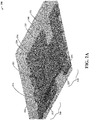
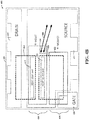
- Figure 2A is a perspective view
- Figure 2B is a top view of a power circuit apparatus 200, as may be implemented in accordance with embodiments of the present disclosure.
- the circuit 200 includes respective transistors in a cascode package based on clip-bond technology, which can be implemented in various manufacturing scenarios (e.g., in an 8x8 mm surface mount outline).
- the circuit 200 includes stacked transistors 210 and 220 arranged in an inverted-stack relationship relative to one another.
- Figure 2B represents an embodiment with transistor 210 being implemented as a high voltage HEMT, and transistor 220 implemented as a low-voltage MOSFET.
- Transistor 210 (e.g., a high-voltage depletion-mode SiC or GaN transistor) includes source 211, drain 212, channel 213 and gate 214.
- Transistor 220 (e.g., a low-voltage enhancement Si MOSFET) includes source 221, drain 222, channel 223 and gate 224.
- a clip 230 connects the source 211 of the first transistor to the drain 222 of the second transistor, and a wire bond 240 connects the source 221 of the second transistor to the gate 214 of the first transistor.
- the second transistor 220 acts to selectively control the first transistor 210 in an off state as well as in an on-state, and therein control power supplied through the apparatus 200.
- the apparatus 200 can be manufactured in a variety of manners.
- respective layers are formed/patterned to provide the stacked circuits as shown.
- a first layer can be formed with the drain 212, source 221 and gate 224 on a common substrate.
- Channel dielectrics 213 and 223 can be respectively formed in a second layer on upper surfaces of the drain 212 and source 221.
- the source 211 and drain 222 can be formed in a third layer on the channel dielectrics along with clip 230 therebetween.
- Gate 214 can be integrated with the first and/or second layers, and arranged to bias a portion of the channel 213 between the source 211 and drain 212.
- connections to the apparatus 200 and between the respective transistors are of a clip or plate type connector, with the exception of the bond wire 240.
- external connections to the apparatus can be made via these components, eliminating inductances that may otherwise be associated with wire bonds to external contacts.
- Terminal connections can be over-molded (hidden) as shown with over-mold 250, and/or conventionally molded (exposed).
- FIG. 3 shows a power circuit 300, as may be implemented in accordance with embodiments of the present disclosure.
- the power circuit 300 may, for example, be implemented using one or more approaches consistent with Figure 2 .
- the power circuit 300 includes a high-voltage power transistor 310, a low-voltage (control) transistor 320, and connecting clip structure 330 that couples the power transistor to the low-voltage transistor (e.g., source to drain).
- the high-voltage power transistor 310 is labeled as a JFET
- the low-voltage transistor 320 is labeled as a MOSFET.
- a connector 340 couples a source of the low-voltage transistor 320 to the gate of the high-voltage transistor 310.
- Table 1 illustrates exemplary package inductance reductions that can be achieved in accordance with one or more embodiments, employing a low-voltage (LV) control transistor and a high-voltage power transistor.
- LV low-voltage
- Table 1 Calculated inductances for wired and clip-bonded packages Inductance Wire Clip-bond External connection to power transistor Tab Tab LV transistor gate contact wire 1.5 nH Pin/0 nH Ground/reference pin contact wire Pin Pin Source-Drain between transistors 1.4 nH 0.64 nH Ground/reference pin to power transistor gate 1.5 nH 2.4 nH ⁇ 1.3 nH* LV source to ground/reference pin 3.5 nH 0 nH * May use a ⁇ 300 ⁇ m wire diameter
- clip-bonding can reduce overall product resistance and inductance, as may be relevant to (but not restricted to) products with a saturation resistance Rds(on) ⁇ 300 mohm.
- the clip type structures can facilitate cooling, reduce manufacturing cost associated with wires, permit higher temperature operation, and facilitate manufacturing assembly automation.
- FIG 4A is a perspective view and Figure 4B is a top view of another power circuit apparatus 400, employing vertical and lateral transistors, as may be implemented in accordance with embodiments of the present disclosure.
- the apparatus 400 includes a lateral high-voltage power transistor 410 having a source 411, drain 412 (pad), channel 413 and gate 414 (as may be located adjacent and/or below the channel).
- the apparatus also includes a vertical low-voltage transistor 420 having source 421, drain 422, channel 423 and gate 424.
- a clip structure 430 connects the drain 422 to the source 411, a clip structure 432 connects the drain 412 to drain contact 415, and a wire 440 connects the source 421 to the gate 414.
- the apparatus 400 may include an over-molding 450, or exhibit exposed wires/connectors.
- Figure 5 shows a cross-sectional view of an apparatus 500 having vertical and lateral transistors, in accordance with one or more embodiments.
- the apparatus 500 may, for example, be implemented using an approach similar to that noted in Figure 4 , with mixed mode operation in which the high-voltage transistor uses lateral current flow and the low-voltage transistor uses vertical flow.
- a high-voltage power transistor 510 is implemented laterally with source 511, drain 512 and channel 513 as shown, on an underlying isolating layer 515 and substrate 516 and with gate 514 on the channel.
- a low-voltage power transistor 520 is implemented vertically with source 521, drain 522 and channel 523 stacked as shown and with gate 524 alongside the channel.
- a clip plate 530 connects the source 511 to drain 522, and a connector 540 completes an electrical connection between the source 521 and the gate 514 (via plate 536).
- Other planar plates can also be implemented, such as plate 532 for connecting the drain 512 to a drain terminal, plate 534 for connecting gate 524 to a gate terminal, and plate 536 for connecting the source 521 to a source terminal (and, e.g., utilized as a support upon which the structure may be formed).
- the low-voltage power transistor 520 controls the operation of the high-voltage transistor 510, which can be effected using a control circuit 550 that provides a voltage for operating the gate 524 and therein controlling the selective application of a voltage from the source 521 to gate 514, for controlling the high-voltage power transistor 510 in an on-state and in an off-state (e.g., with voltage respectively not applied/floating and voltage applied).
- a control circuit 550 that provides a voltage for operating the gate 524 and therein controlling the selective application of a voltage from the source 521 to gate 514, for controlling the high-voltage power transistor 510 in an on-state and in an off-state (e.g., with voltage respectively not applied/floating and voltage applied).
- orientation such as upper/lower, left/right, top/bottom and above/below, may be used herein to refer to relative positions of elements as shown in the figures. It should be understood that when the terminology is used for notational convenience, the disclosed structures may be oriented different from the orientation shown in the figures. For instance, high-voltage power transistors and low-voltage transistors can be flipped relative to one another in opposing stacked arrangements.
- circuits or circuitry which may be discussed or otherwise considered using terms such as blocks, modules, device, system, unit, controller, comparator, and other circuit-type depictions. Such circuits or circuitry are discussed in connection with other elements to explain how certain embodiments may be carried out.
- one or more illustrated items in this context represent circuits (e.g., discrete analog or logic circuitry or (semi-)programmable circuits) configured and arranged for implementing disclosed operations/activities, as may be carried out in the approaches shown in the figures.
Landscapes
- Engineering & Computer Science (AREA)
- Microelectronics & Electronic Packaging (AREA)
- Computer Hardware Design (AREA)
- Power Engineering (AREA)
- Physics & Mathematics (AREA)
- Condensed Matter Physics & Semiconductors (AREA)
- General Physics & Mathematics (AREA)
- Manufacturing & Machinery (AREA)
- Metal-Oxide And Bipolar Metal-Oxide Semiconductor Integrated Circuits (AREA)
- Junction Field-Effect Transistors (AREA)
- Thin Film Transistor (AREA)
Priority Applications (3)
| Application Number | Priority Date | Filing Date | Title |
|---|---|---|---|
| EP17164854.6A EP3385981A1 (fr) | 2017-04-04 | 2017-04-04 | Appareil d'alimentation |
| CN201810300420.XA CN108695308B (zh) | 2017-04-04 | 2018-04-04 | 电源设备 |
| US15/944,855 US10665532B2 (en) | 2017-04-04 | 2018-04-04 | Power apparatus |
Applications Claiming Priority (1)
| Application Number | Priority Date | Filing Date | Title |
|---|---|---|---|
| EP17164854.6A EP3385981A1 (fr) | 2017-04-04 | 2017-04-04 | Appareil d'alimentation |
Publications (1)
| Publication Number | Publication Date |
|---|---|
| EP3385981A1 true EP3385981A1 (fr) | 2018-10-10 |
Family
ID=58489568
Family Applications (1)
| Application Number | Title | Priority Date | Filing Date |
|---|---|---|---|
| EP17164854.6A Pending EP3385981A1 (fr) | 2017-04-04 | 2017-04-04 | Appareil d'alimentation |
Country Status (3)
| Country | Link |
|---|---|
| US (1) | US10665532B2 (fr) |
| EP (1) | EP3385981A1 (fr) |
| CN (1) | CN108695308B (fr) |
Cited By (1)
| Publication number | Priority date | Publication date | Assignee | Title |
|---|---|---|---|---|
| EP4044225A1 (fr) * | 2021-02-16 | 2022-08-17 | Nexperia B.V. | Dispositif à semi-conducteur et procédé de fabrication d'un dispositif à semi-conducteur |
Families Citing this family (1)
| Publication number | Priority date | Publication date | Assignee | Title |
|---|---|---|---|---|
| US10886201B2 (en) * | 2018-02-15 | 2021-01-05 | Epistar Corporation | Power device having a substrate with metal layers exposed at surfaces of an insulation layer and manufacturing method thereof |
Citations (5)
| Publication number | Priority date | Publication date | Assignee | Title |
|---|---|---|---|---|
| US20120250587A1 (en) | 2011-03-30 | 2012-10-04 | Sujan Pandey | Full duplex communication circuit and method therefor |
| US20140033410A1 (en) | 2012-08-06 | 2014-02-06 | Lion Apparel, Inc. | Protective Garment with Elastic Thermal Barrier Portions |
| US20140145208A1 (en) | 2012-11-23 | 2014-05-29 | Nxp B.V. | Cascoded semiconductor devices |
| US20140217596A1 (en) * | 2013-02-05 | 2014-08-07 | Infineon Technologies Austria Ag | Power transistor arrangement and method for manufacturing the same |
| US20150041984A1 (en) * | 2013-08-09 | 2015-02-12 | Infineon Technologies Austria Ag | Electronic Component and Method |
Family Cites Families (9)
| Publication number | Priority date | Publication date | Assignee | Title |
|---|---|---|---|---|
| CN1906852A (zh) * | 2004-01-19 | 2007-01-31 | 皇家飞利浦电子股份有限公司 | Mos开关电路 |
| JP5107839B2 (ja) * | 2008-09-10 | 2012-12-26 | ルネサスエレクトロニクス株式会社 | 半導体装置 |
| US9515060B2 (en) * | 2013-03-20 | 2016-12-06 | Infineon Technologies Austria Ag | Multi-chip semiconductor power device |
| EP2787641B1 (fr) | 2013-04-05 | 2018-08-29 | Nexperia B.V. | Dispositifs à semi-conducteurs cascadés |
| US9570379B2 (en) * | 2013-12-09 | 2017-02-14 | Infineon Technologies Americas Corp. | Power semiconductor package with integrated heat spreader and partially etched conductive carrier |
| JP6139710B2 (ja) * | 2014-01-27 | 2017-05-31 | 三菱電機株式会社 | 電極端子、電力用半導体装置、および電力用半導体装置の製造方法 |
| US9496207B1 (en) * | 2015-06-19 | 2016-11-15 | Semiconductor Components Industries, Llc | Cascode semiconductor package and related methods |
| US10128174B2 (en) * | 2015-07-24 | 2018-11-13 | Semiconductor Components Industries, Llc | Semiconductor component and method of manufacture |
| US20180182730A1 (en) * | 2016-12-23 | 2018-06-28 | Infineon Technologies Americas Corp. | Common contact semiconductor device package |
-
2017
- 2017-04-04 EP EP17164854.6A patent/EP3385981A1/fr active Pending
-
2018
- 2018-04-04 US US15/944,855 patent/US10665532B2/en active Active
- 2018-04-04 CN CN201810300420.XA patent/CN108695308B/zh active Active
Patent Citations (5)
| Publication number | Priority date | Publication date | Assignee | Title |
|---|---|---|---|---|
| US20120250587A1 (en) | 2011-03-30 | 2012-10-04 | Sujan Pandey | Full duplex communication circuit and method therefor |
| US20140033410A1 (en) | 2012-08-06 | 2014-02-06 | Lion Apparel, Inc. | Protective Garment with Elastic Thermal Barrier Portions |
| US20140145208A1 (en) | 2012-11-23 | 2014-05-29 | Nxp B.V. | Cascoded semiconductor devices |
| US20140217596A1 (en) * | 2013-02-05 | 2014-08-07 | Infineon Technologies Austria Ag | Power transistor arrangement and method for manufacturing the same |
| US20150041984A1 (en) * | 2013-08-09 | 2015-02-12 | Infineon Technologies Austria Ag | Electronic Component and Method |
Cited By (1)
| Publication number | Priority date | Publication date | Assignee | Title |
|---|---|---|---|---|
| EP4044225A1 (fr) * | 2021-02-16 | 2022-08-17 | Nexperia B.V. | Dispositif à semi-conducteur et procédé de fabrication d'un dispositif à semi-conducteur |
Also Published As
| Publication number | Publication date |
|---|---|
| US20180286792A1 (en) | 2018-10-04 |
| CN108695308A (zh) | 2018-10-23 |
| US10665532B2 (en) | 2020-05-26 |
| CN108695308B (zh) | 2023-11-03 |
Similar Documents
| Publication | Publication Date | Title |
|---|---|---|
| JP7167198B2 (ja) | 高電圧電力モジュール | |
| US9818686B2 (en) | Semiconductor modules and methods of forming the same | |
| JP7056836B2 (ja) | 高電流、低スイッチングロスのSiCパワーモジュール | |
| US8461669B2 (en) | Integrated power converter package with die stacking | |
| US9443787B2 (en) | Electronic component and method | |
| US10903158B2 (en) | Semiconductor arrangement having a circuit board with a patterned metallization layer | |
| CN105280625A (zh) | 半导体装置和电子设备 | |
| US10074597B2 (en) | Interdigit device on leadframe for evenly distributed current flow | |
| CN110226226A (zh) | 由层叠的两个串联连接的芯片形成的集成电路 | |
| CN107833885B (zh) | 功率开关器件 | |
| US10665532B2 (en) | Power apparatus | |
| US8023276B2 (en) | Circuit arrangement comprising having plurality of half bridges | |
| US10790249B2 (en) | Discrete electronic component comprising a transistor | |
| TWI846560B (zh) | 封裝結構 | |
| TWI850113B (zh) | 功率模組封裝結構以及功率電晶體 | |
| EP3396839A1 (fr) | Agencement semi-conducteur avec des éléments à semi-conducteur commandables | |
| WO2023122694A2 (fr) | Ensemble module de multiples dispositifs à semi-conducteurs comprenant des substrats isolants | |
| CN118538696A (zh) | 半导体装置 | |
| JP2005005857A (ja) | スイッチ回路装置 |
Legal Events
| Date | Code | Title | Description |
|---|---|---|---|
| PUAI | Public reference made under article 153(3) epc to a published international application that has entered the european phase |
Free format text: ORIGINAL CODE: 0009012 |
|
| STAA | Information on the status of an ep patent application or granted ep patent |
Free format text: STATUS: THE APPLICATION HAS BEEN PUBLISHED |
|
| AK | Designated contracting states |
Kind code of ref document: A1 Designated state(s): AL AT BE BG CH CY CZ DE DK EE ES FI FR GB GR HR HU IE IS IT LI LT LU LV MC MK MT NL NO PL PT RO RS SE SI SK SM TR |
|
| AX | Request for extension of the european patent |
Extension state: BA ME |
|
| STAA | Information on the status of an ep patent application or granted ep patent |
Free format text: STATUS: REQUEST FOR EXAMINATION WAS MADE |
|
| 17P | Request for examination filed |
Effective date: 20190408 |
|
| RBV | Designated contracting states (corrected) |
Designated state(s): AL AT BE BG CH CY CZ DE DK EE ES FI FR GB GR HR HU IE IS IT LI LT LU LV MC MK MT NL NO PL PT RO RS SE SI SK SM TR |
|
| STAA | Information on the status of an ep patent application or granted ep patent |
Free format text: STATUS: EXAMINATION IS IN PROGRESS |
|
| 17Q | First examination report despatched |
Effective date: 20210129 |
|
| STAA | Information on the status of an ep patent application or granted ep patent |
Free format text: STATUS: EXAMINATION IS IN PROGRESS |