EP3385367B1 - Microfluidic system for cultivating or analysing living cells or biomolecules, and a method for its manufacture - Google Patents
Microfluidic system for cultivating or analysing living cells or biomolecules, and a method for its manufacture Download PDFInfo
- Publication number
- EP3385367B1 EP3385367B1 EP18165888.1A EP18165888A EP3385367B1 EP 3385367 B1 EP3385367 B1 EP 3385367B1 EP 18165888 A EP18165888 A EP 18165888A EP 3385367 B1 EP3385367 B1 EP 3385367B1
- Authority
- EP
- European Patent Office
- Prior art keywords
- laminate
- sensor
- laminates
- actuator
- electrical
- Prior art date
- Legal status (The legal status is an assumption and is not a legal conclusion. Google has not performed a legal analysis and makes no representation as to the accuracy of the status listed.)
- Active
Links
- 238000004519 manufacturing process Methods 0.000 title claims description 21
- 238000000034 method Methods 0.000 title claims description 18
- 239000012528 membrane Substances 0.000 claims description 28
- 239000000919 ceramic Substances 0.000 claims description 19
- 239000000463 material Substances 0.000 claims description 19
- 239000004020 conductor Substances 0.000 claims description 16
- 239000007788 liquid Substances 0.000 claims description 15
- 239000004065 semiconductor Substances 0.000 claims description 11
- QVGXLLKOCUKJST-UHFFFAOYSA-N atomic oxygen Chemical compound [O] QVGXLLKOCUKJST-UHFFFAOYSA-N 0.000 claims description 7
- 239000001301 oxygen Substances 0.000 claims description 7
- 229910052760 oxygen Inorganic materials 0.000 claims description 7
- 238000007669 thermal treatment Methods 0.000 claims description 7
- 238000007639 printing Methods 0.000 claims description 6
- WQZGKKKJIJFFOK-GASJEMHNSA-N Glucose Natural products OC[C@H]1OC(O)[C@H](O)[C@@H](O)[C@@H]1O WQZGKKKJIJFFOK-GASJEMHNSA-N 0.000 claims description 3
- 230000005670 electromagnetic radiation Effects 0.000 claims description 3
- 239000008103 glucose Substances 0.000 claims description 3
- 239000000203 mixture Substances 0.000 claims description 3
- 238000005245 sintering Methods 0.000 claims description 3
- JVTAAEKCZFNVCJ-UHFFFAOYSA-M Lactate Chemical compound CC(O)C([O-])=O JVTAAEKCZFNVCJ-UHFFFAOYSA-M 0.000 claims description 2
- 238000004458 analytical method Methods 0.000 claims description 2
- 230000001939 inductive effect Effects 0.000 claims description 2
- 238000012258 culturing Methods 0.000 claims 2
- 239000002861 polymer material Substances 0.000 claims 1
- 210000004379 membrane Anatomy 0.000 description 22
- 210000004027 cell Anatomy 0.000 description 21
- 238000005516 engineering process Methods 0.000 description 12
- 238000005304 joining Methods 0.000 description 10
- 229920000642 polymer Polymers 0.000 description 10
- 239000000758 substrate Substances 0.000 description 10
- 239000002105 nanoparticle Substances 0.000 description 9
- 230000010354 integration Effects 0.000 description 7
- 230000008569 process Effects 0.000 description 7
- -1 antibodies Proteins 0.000 description 6
- 238000004113 cell culture Methods 0.000 description 6
- 239000003792 electrolyte Substances 0.000 description 6
- 230000003287 optical effect Effects 0.000 description 6
- 230000008901 benefit Effects 0.000 description 5
- 239000007789 gas Substances 0.000 description 5
- 239000000976 ink Substances 0.000 description 5
- 239000002245 particle Substances 0.000 description 5
- 239000002131 composite material Substances 0.000 description 4
- 239000011888 foil Substances 0.000 description 4
- PCHJSUWPFVWCPO-UHFFFAOYSA-N gold Chemical compound [Au] PCHJSUWPFVWCPO-UHFFFAOYSA-N 0.000 description 4
- 229910052737 gold Inorganic materials 0.000 description 4
- 239000010931 gold Substances 0.000 description 4
- 229910052710 silicon Inorganic materials 0.000 description 4
- 239000010703 silicon Substances 0.000 description 4
- 239000000126 substance Substances 0.000 description 4
- 239000004642 Polyimide Substances 0.000 description 3
- 238000004026 adhesive bonding Methods 0.000 description 3
- 229910010293 ceramic material Inorganic materials 0.000 description 3
- 239000004205 dimethyl polysiloxane Substances 0.000 description 3
- 239000012530 fluid Substances 0.000 description 3
- 238000000608 laser ablation Methods 0.000 description 3
- 230000002093 peripheral effect Effects 0.000 description 3
- 229920000435 poly(dimethylsiloxane) Polymers 0.000 description 3
- 239000004417 polycarbonate Substances 0.000 description 3
- 229920000515 polycarbonate Polymers 0.000 description 3
- 229920001721 polyimide Polymers 0.000 description 3
- 238000003825 pressing Methods 0.000 description 3
- 238000007650 screen-printing Methods 0.000 description 3
- 230000001953 sensory effect Effects 0.000 description 3
- CURLTUGMZLYLDI-UHFFFAOYSA-N Carbon dioxide Chemical compound O=C=O CURLTUGMZLYLDI-UHFFFAOYSA-N 0.000 description 2
- RYGMFSIKBFXOCR-UHFFFAOYSA-N Copper Chemical compound [Cu] RYGMFSIKBFXOCR-UHFFFAOYSA-N 0.000 description 2
- 229920000089 Cyclic olefin copolymer Polymers 0.000 description 2
- 239000004696 Poly ether ether ketone Substances 0.000 description 2
- 239000004698 Polyethylene Substances 0.000 description 2
- 239000004743 Polypropylene Substances 0.000 description 2
- VYPSYNLAJGMNEJ-UHFFFAOYSA-N Silicium dioxide Chemical compound O=[Si]=O VYPSYNLAJGMNEJ-UHFFFAOYSA-N 0.000 description 2
- XUIMIQQOPSSXEZ-UHFFFAOYSA-N Silicon Chemical compound [Si] XUIMIQQOPSSXEZ-UHFFFAOYSA-N 0.000 description 2
- 239000000443 aerosol Substances 0.000 description 2
- WQZGKKKJIJFFOK-VFUOTHLCSA-N beta-D-glucose Chemical compound OC[C@H]1O[C@@H](O)[C@H](O)[C@@H](O)[C@@H]1O WQZGKKKJIJFFOK-VFUOTHLCSA-N 0.000 description 2
- 230000015572 biosynthetic process Effects 0.000 description 2
- 239000000969 carrier Substances 0.000 description 2
- 230000019522 cellular metabolic process Effects 0.000 description 2
- 238000010276 construction Methods 0.000 description 2
- 238000013461 design Methods 0.000 description 2
- 238000010017 direct printing Methods 0.000 description 2
- 238000004049 embossing Methods 0.000 description 2
- 230000005284 excitation Effects 0.000 description 2
- 230000009477 glass transition Effects 0.000 description 2
- 238000010438 heat treatment Methods 0.000 description 2
- 238000007641 inkjet printing Methods 0.000 description 2
- 238000010030 laminating Methods 0.000 description 2
- 230000004060 metabolic process Effects 0.000 description 2
- 238000012544 monitoring process Methods 0.000 description 2
- 230000005693 optoelectronics Effects 0.000 description 2
- BASFCYQUMIYNBI-UHFFFAOYSA-N platinum Chemical compound [Pt] BASFCYQUMIYNBI-UHFFFAOYSA-N 0.000 description 2
- 229920003229 poly(methyl methacrylate) Polymers 0.000 description 2
- 229920002530 polyetherether ketone Polymers 0.000 description 2
- 229920000573 polyethylene Polymers 0.000 description 2
- 229920000139 polyethylene terephthalate Polymers 0.000 description 2
- 239000005020 polyethylene terephthalate Substances 0.000 description 2
- 229920006254 polymer film Polymers 0.000 description 2
- 239000004926 polymethyl methacrylate Substances 0.000 description 2
- 229920001155 polypropylene Polymers 0.000 description 2
- 229920001296 polysiloxane Polymers 0.000 description 2
- 229920001343 polytetrafluoroethylene Polymers 0.000 description 2
- 239000004810 polytetrafluoroethylene Substances 0.000 description 2
- 239000010970 precious metal Substances 0.000 description 2
- 230000009467 reduction Effects 0.000 description 2
- 238000007789 sealing Methods 0.000 description 2
- 238000003786 synthesis reaction Methods 0.000 description 2
- 229920001169 thermoplastic Polymers 0.000 description 2
- 229920002725 thermoplastic elastomer Polymers 0.000 description 2
- 239000004416 thermosoftening plastic Substances 0.000 description 2
- SWPMTVXRLXPNDP-UHFFFAOYSA-N 4-hydroxy-2,6,6-trimethylcyclohexene-1-carbaldehyde Chemical compound CC1=C(C=O)C(C)(C)CC(O)C1 SWPMTVXRLXPNDP-UHFFFAOYSA-N 0.000 description 1
- 239000004793 Polystyrene Substances 0.000 description 1
- 229910052581 Si3N4 Inorganic materials 0.000 description 1
- BQCADISMDOOEFD-UHFFFAOYSA-N Silver Chemical compound [Ag] BQCADISMDOOEFD-UHFFFAOYSA-N 0.000 description 1
- 238000002679 ablation Methods 0.000 description 1
- 239000013543 active substance Substances 0.000 description 1
- 229910045601 alloy Inorganic materials 0.000 description 1
- 239000000956 alloy Substances 0.000 description 1
- 238000009530 blood pressure measurement Methods 0.000 description 1
- 239000003990 capacitor Substances 0.000 description 1
- 229910002092 carbon dioxide Inorganic materials 0.000 description 1
- 239000001569 carbon dioxide Substances 0.000 description 1
- 239000012876 carrier material Substances 0.000 description 1
- 230000003750 conditioning effect Effects 0.000 description 1
- 238000011109 contamination Methods 0.000 description 1
- 238000001816 cooling Methods 0.000 description 1
- 229910052802 copper Inorganic materials 0.000 description 1
- 239000010949 copper Substances 0.000 description 1
- 239000011889 copper foil Substances 0.000 description 1
- PMHQVHHXPFUNSP-UHFFFAOYSA-M copper(1+);methylsulfanylmethane;bromide Chemical compound Br[Cu].CSC PMHQVHHXPFUNSP-UHFFFAOYSA-M 0.000 description 1
- 210000004748 cultured cell Anatomy 0.000 description 1
- 238000005520 cutting process Methods 0.000 description 1
- 150000001925 cycloalkenes Chemical class 0.000 description 1
- 238000001514 detection method Methods 0.000 description 1
- 238000011161 development Methods 0.000 description 1
- 230000018109 developmental process Effects 0.000 description 1
- 238000009792 diffusion process Methods 0.000 description 1
- 238000007599 discharging Methods 0.000 description 1
- 229920001971 elastomer Polymers 0.000 description 1
- 239000000806 elastomer Substances 0.000 description 1
- 238000001962 electrophoresis Methods 0.000 description 1
- 238000003891 environmental analysis Methods 0.000 description 1
- 238000001704 evaporation Methods 0.000 description 1
- 230000008020 evaporation Effects 0.000 description 1
- 239000000835 fiber Substances 0.000 description 1
- 238000011049 filling Methods 0.000 description 1
- 230000004927 fusion Effects 0.000 description 1
- 239000001963 growth medium Substances 0.000 description 1
- 210000005260 human cell Anatomy 0.000 description 1
- 238000009396 hybridization Methods 0.000 description 1
- 230000006872 improvement Effects 0.000 description 1
- 238000002347 injection Methods 0.000 description 1
- 239000007924 injection Substances 0.000 description 1
- 238000001746 injection moulding Methods 0.000 description 1
- 238000009434 installation Methods 0.000 description 1
- 238000003475 lamination Methods 0.000 description 1
- 238000009766 low-temperature sintering Methods 0.000 description 1
- 238000005259 measurement Methods 0.000 description 1
- 235000015097 nutrients Nutrition 0.000 description 1
- TWNQGVIAIRXVLR-UHFFFAOYSA-N oxo(oxoalumanyloxy)alumane Chemical compound O=[Al]O[Al]=O TWNQGVIAIRXVLR-UHFFFAOYSA-N 0.000 description 1
- RVTZCBVAJQQJTK-UHFFFAOYSA-N oxygen(2-);zirconium(4+) Chemical compound [O-2].[O-2].[Zr+4] RVTZCBVAJQQJTK-UHFFFAOYSA-N 0.000 description 1
- 238000001139 pH measurement Methods 0.000 description 1
- 239000012466 permeate Substances 0.000 description 1
- 238000000678 plasma activation Methods 0.000 description 1
- 229910052697 platinum Inorganic materials 0.000 description 1
- 238000007781 pre-processing Methods 0.000 description 1
- 238000012545 processing Methods 0.000 description 1
- 102000004169 proteins and genes Human genes 0.000 description 1
- 108090000623 proteins and genes Proteins 0.000 description 1
- 238000004080 punching Methods 0.000 description 1
- 230000000717 retained effect Effects 0.000 description 1
- 235000012239 silicon dioxide Nutrition 0.000 description 1
- 239000000377 silicon dioxide Substances 0.000 description 1
- HQVNEWCFYHHQES-UHFFFAOYSA-N silicon nitride Chemical compound N12[Si]34N5[Si]62N3[Si]51N64 HQVNEWCFYHHQES-UHFFFAOYSA-N 0.000 description 1
- 229910052709 silver Inorganic materials 0.000 description 1
- 239000004332 silver Substances 0.000 description 1
- 238000005476 soldering Methods 0.000 description 1
- 239000000243 solution Substances 0.000 description 1
- 230000004936 stimulating effect Effects 0.000 description 1
- 230000000638 stimulation Effects 0.000 description 1
- 238000000859 sublimation Methods 0.000 description 1
- 230000008022 sublimation Effects 0.000 description 1
- 239000000725 suspension Substances 0.000 description 1
- 230000000007 visual effect Effects 0.000 description 1
- 229910001928 zirconium oxide Inorganic materials 0.000 description 1
Images


Classifications
-
- C—CHEMISTRY; METALLURGY
- C12—BIOCHEMISTRY; BEER; SPIRITS; WINE; VINEGAR; MICROBIOLOGY; ENZYMOLOGY; MUTATION OR GENETIC ENGINEERING
- C12M—APPARATUS FOR ENZYMOLOGY OR MICROBIOLOGY; APPARATUS FOR CULTURING MICROORGANISMS FOR PRODUCING BIOMASS, FOR GROWING CELLS OR FOR OBTAINING FERMENTATION OR METABOLIC PRODUCTS, i.e. BIOREACTORS OR FERMENTERS
- C12M23/00—Constructional details, e.g. recesses, hinges
- C12M23/02—Form or structure of the vessel
- C12M23/16—Microfluidic devices; Capillary tubes
-
- C—CHEMISTRY; METALLURGY
- C12—BIOCHEMISTRY; BEER; SPIRITS; WINE; VINEGAR; MICROBIOLOGY; ENZYMOLOGY; MUTATION OR GENETIC ENGINEERING
- C12M—APPARATUS FOR ENZYMOLOGY OR MICROBIOLOGY; APPARATUS FOR CULTURING MICROORGANISMS FOR PRODUCING BIOMASS, FOR GROWING CELLS OR FOR OBTAINING FERMENTATION OR METABOLIC PRODUCTS, i.e. BIOREACTORS OR FERMENTERS
- C12M23/00—Constructional details, e.g. recesses, hinges
- C12M23/22—Transparent or translucent parts
-
- C—CHEMISTRY; METALLURGY
- C12—BIOCHEMISTRY; BEER; SPIRITS; WINE; VINEGAR; MICROBIOLOGY; ENZYMOLOGY; MUTATION OR GENETIC ENGINEERING
- C12M—APPARATUS FOR ENZYMOLOGY OR MICROBIOLOGY; APPARATUS FOR CULTURING MICROORGANISMS FOR PRODUCING BIOMASS, FOR GROWING CELLS OR FOR OBTAINING FERMENTATION OR METABOLIC PRODUCTS, i.e. BIOREACTORS OR FERMENTERS
- C12M35/00—Means for application of stress for stimulating the growth of microorganisms or the generation of fermentation or metabolic products; Means for electroporation or cell fusion
-
- C—CHEMISTRY; METALLURGY
- C12—BIOCHEMISTRY; BEER; SPIRITS; WINE; VINEGAR; MICROBIOLOGY; ENZYMOLOGY; MUTATION OR GENETIC ENGINEERING
- C12M—APPARATUS FOR ENZYMOLOGY OR MICROBIOLOGY; APPARATUS FOR CULTURING MICROORGANISMS FOR PRODUCING BIOMASS, FOR GROWING CELLS OR FOR OBTAINING FERMENTATION OR METABOLIC PRODUCTS, i.e. BIOREACTORS OR FERMENTERS
- C12M41/00—Means for regulation, monitoring, measurement or control, e.g. flow regulation
- C12M41/12—Means for regulation, monitoring, measurement or control, e.g. flow regulation of temperature
-
- C—CHEMISTRY; METALLURGY
- C12—BIOCHEMISTRY; BEER; SPIRITS; WINE; VINEGAR; MICROBIOLOGY; ENZYMOLOGY; MUTATION OR GENETIC ENGINEERING
- C12M—APPARATUS FOR ENZYMOLOGY OR MICROBIOLOGY; APPARATUS FOR CULTURING MICROORGANISMS FOR PRODUCING BIOMASS, FOR GROWING CELLS OR FOR OBTAINING FERMENTATION OR METABOLIC PRODUCTS, i.e. BIOREACTORS OR FERMENTERS
- C12M41/00—Means for regulation, monitoring, measurement or control, e.g. flow regulation
- C12M41/46—Means for regulation, monitoring, measurement or control, e.g. flow regulation of cellular or enzymatic activity or functionality, e.g. cell viability
Definitions
- the invention relates to a microfluidic system for cultivating or analyzing living cells or biomolecules and a method for its production.
- a wide variety of examinations and influence options can be carried out and monitored on living cells. For example, the influence of certain influencing factors or Substances on the metabolism of cells can be detected.
- the system is also suitable for examining various biomolecules such as proteins, antibodies, DNA or RNA.
- Polymer carrier materials are currently primarily used for cell cultivation. This is mainly due to the good biocompatibility, the low production price (injection molding) and the good visual accessibility.
- electrochemical sensors for example for measuring the trans-epithelial resistance (TEER) can only be introduced externally, for example in the form of chopstick electrodes.
- the direct implementation of such sensors would bring a number of advantages (reduction of the dead volume, improvement of the measurement signal, reduction of contamination, ).
- Ceramic sensors are ideal here, in which the electrochemically active layers are applied in a structured manner using a screen printing process and then burned in.
- Multi-layer constructions such as multi-layer printed circuit boards with buried components on Si or ceramic substrates
- Multi-layer structures on polymer carriers are used, which enclose and electrically contact other materials.
- Common substrates are fiber composites, such as FR-4, or polymer films, such as polyimide, onto which copper foil is laminated. These materials have no or only limited biocompatibility or are not sufficiently transparent and are therefore unsuitable for use in cell cultivation.
- microfluidic systems that are also used for cell cultivation and have a comparatively high integration density and contain sensors and/or actuators.
- glass-silicon hybrid systems are used, with both the structuring of the microfluidic channels and the production of the sensors or actuators and their electrical contacting mostly being carried out lithographically.
- the structured layers are then joined to form a fluid-tight composite, preferably by means of anodic bonding.
- Disadvantages of this production technology are on the one hand the high costs due to the required lithographic equipment, the expensive substrate materials and the Masks and, on the other hand, the low production yield, since many complex production steps have to be carried out one after the other.
- DE 10 2010 038 445 A1 relates to a method for producing a microfluidic system.
- a microfluidic device for manipulating and analyzing fluids is in U.S. 2005/0106066 A1 disclosed.
- At least one opening or at least one cutout is formed in one of the laminates, with which a channel or a reservoir for receiving living cells or biomolecules is formed.
- at least one further opening is formed in at least one of the laminates, into which an actuator and/or sensor made of a ceramic or a semiconducting material or a carrier for an actuator or sensor made of a ceramic or semiconducting material is inserted.
- An actuator and/or sensor should be arranged and designed in such a way that contact with a liquid containing living cells or biomolecules or direct contact with living cells or biomolecules is possible. At least one actuator and/or sensor is therefore in touching contact with a liquid for the cultivation of cells, a liquid containing biomolecules or the cells or biomolecules contained in a channel or reservoir.
- At least one electrical conductor track is printed, with which an electrical contact of the actuator and / or sensor can be achieved. This can also be done by overprinting the connection contacts of the sensor/actuator or by mechanically pressing the same onto the printed circuit board.
- An actuator and/or sensor can be arranged on a surface of a carrier or in a carrier.
- LTCC, HTCC or monolithic materials such as aluminum oxide, zirconium oxide, silicon nitride or aluminum nitride can be used as ceramic materials.
- Silicon in undoped or doped form or silicon dioxide can be used as the semiconducting material.
- the laminates are foils and/or panel-shaped workpieces.
- the laminates that form a system should, if possible, consist of the same material or at least consist of very similar polymeric materials, which particularly relates to the glass transition temperature.
- At least one of the laminates there can be at least one electrical via, in which an electrically conductive material is contained in an opening.
- an elastically deformable, electrically conductive contact element can consist of a precious metal, in particular gold, or be coated with it.
- the openings should be designed and dimensioned geometrically in such a way that an actuator and/or sensor or a carrier or an elastically deformable electrically conductive element is held in a form-fitting manner with a corresponding design at its edge.
- a flexibly deformable printed circuit board can be arranged between two laminates arranged one above the other and connected to the laminates in a fluid-tight manner.
- the circuit board can accordingly with electrical and / or electronic components that are connected to each other via electrical conductor tracks, be equipped.
- Electrically conductive connections to an actuator or sensor can be achieved via electrical through-connections (vias) or with elastically deformable electrically conductive elements.
- a sensor arranged within the stack formed with the laminates can be used to record physical quantities, e.g. temperature, flow, volume flow, pressure, electromagnetic radiation, electrical conductivity or the material composition (e.g. the oxygen, glucose or lactate content) or be an actuator .
- Actuators can be, for example, pneumatically, thermopneumatically, electrostatically, piezoelectrically, electromechanically driven membranes or pistons. Actuators can also be electrodes for electrical cell stimulation, electrodes for cell/particle manipulation or deflection with di/electrophoresis, optoelectronic components or piezoelectric actuators and temperature control elements for cooling or heating.
- At least one permeable membrane preferably a gas-permeable membrane
- a permeable membrane can be arranged in the area of a channel or reservoir. This opens up the possibility of discharging formed gases or supplying gas. For example, gases formed as a result of metabolism can be discharged and oxygen can be supplied for the supply of nutrients. These can then be detected, in particular with regard to their composition and the respective volumes, and any influence on the metabolism that may have occurred can be recognized and readjusted.
- Gas-permeable membranes can be formed from silicone foils, thin thermoplastics or thermoplastic elastomers (TPE), for example.
- Porous membranes e.g. laser-structured or track-etched PC film
- a system according to the invention e.g. as cell carriers or for the production of electrochemical sensors.
- a channel or reservoir can be connected to an inlet and/or outlet for a liquid which can contain living cells and/or biomolecules.
- a connecting piece can be passed through an outwardly directed opening, which is in at least is formed of a laminate, is introduced and a fluid-tight and materially bonded connection is formed with the respective laminate.
- electrical and/or electronic elements in particular an electrical resistor, an inductive electrical element, a capacitive electrical element or a transistor, are formed on at least one surface of at least one laminate by means of a printing process.
- Sensory elements such as strain gauges for pressure measurement or electrode structures, e.g. for particle or cell manipulation, can also be printed directly using this process.
- a channel or a reservoir can be covered at least in regions with a semipermeable membrane on a laminate.
- the membrane can be permeable to a gas and possibly impermeable to a liquid, such as an electrolyte.
- oxygen or carbon dioxide can permeate through the membrane and in a further channel or reservoir arranged there on the other side of the membrane, on which, for example, no cell cultures are present in an opening, a suitable sensor determining the respective gas concentration can be arranged with which studies of the metabolism of cell cultures can be carried out.
- a channel or a reservoir can also be covered at least in regions with an elastically deformable membrane, in which case the membrane can be imprinted with electrically conductive printed structures, in particular strain gauges. This makes it possible, for example, to measure the pressure in the system.
- One or more membrane(s) can be laminated in between adjacent laminates when the laminates are joined and can be cohesively connected to the respective surfaces of the laminates touching the membrane surface in a fluid-tight manner at the outer edge of the respective membrane.
- the procedure is such that in at least one laminate between an above and is to be arranged underneath the laminate, at least one opening or recess for forming a channel or reservoir and in at least one laminate to be arranged above or below this laminate at least one further opening for receiving an actuator and/or sensor made of ceramic or semiconducting material or a carrier an actuator and/or sensor, which is made of a ceramic or semiconducting material.
- At least one electrical conductor track for electrical contacting of the actuator and/or sensor is formed using a printing process on a surface of this laminate or of a laminate to be arranged directly adjacent.
- the laminates are then arranged one on top of the other in such a way that the at least one opening forming a channel or a reservoir and the at least one actuator and/or sensor are positioned relative to one another and the laminates forming the stack are fluid-tight and cohesively bonded to one another by thermal treatment and preferably compressive forces acting at the same time get connected.
- the openings can be formed by stamping, embossing, mechanical material removal, laser beam cutting and ablation, or lithographically.
- channels or reservoirs with dimensions in the range from 10 ⁇ m to 5 mm, in particular their height and width, can be formed.
- a channel can have a significantly greater length and also not be aligned exclusively along a straight longitudinal axis, but also be designed in an arc shape at least in some areas.
- the imprinting of electrical conductor tracks and possibly other electrical and/or electronic components can be achieved with direct-writing methods (aerosol jet or inkjet printing) of inks containing nanoparticles or with screen printing (polymeric pastes/pastes containing nanoparticles).
- direct-writing methods as inosol jet or inkjet printing
- screen printing polymeric pastes/pastes containing nanoparticles.
- Common connection techniques such as soldering and/or elastically deformable contact elements can also be used to produce an electrical contact with peripheral electronics.
- Known pastes or suspensions can be used for printing and also for the production of electrically conductive plated-through holes. These contain electrically conductive particles which can be at least partially sintered together during a thermal treatment. Liquid and polymeric components can be removed by evaporation or by sublimation.
- At least one channel or at least one reservoir may be formed with openings or recesses formed in a plurality of laminates disposed adjacent one another in the laminate stack. In this way, three-dimensional fluid systems can also be formed over several layers.
- Fluidic structures in the form of channels and/or reservoirs can be formed not only in laminates but also on a ceramic or semiconducting material, such as a carrier, for example. These structures may be connected to channels and/or a reservoir formed in the laminate stack.
- Micromixers or particle sorters can be implemented with fluidic structures.
- Recesses can extend to the outer edge so that liquid can be supplied and removed from there.
- polycarbonate for example, polycarbonate (PC), cyclo-olefin copolymer (COC), polyethylene (PE), polyethylene terephthalate (PET), polypropylene (PP), polystyrene (PS), polyimide (PI), polymethyl methacrylate (PMMA), polyetheretherketone (PEEK), polytetrafluoroethylene (PTFE) or silicones such as polydimethylsiloxane (PDMS) and other polyorganosiloxanes are used as polymeric material.
- PC polycarbonate
- COC cyclo-olefin copolymer
- PE polyethylene
- PET polyethylene terephthalate
- PP polypropylene
- PS polystyrene
- PI polyimide
- PMMA polymethyl methacrylate
- PEEK polyetheretherketone
- PTFE polytetrafluoroethylene
- silicones such as polydimethylsiloxane (PDMS) and other polyorganosilox
- Thermal diffusion bonding plasma joining, wet-chemical methods, laser-assisted joining, ultrasonic joining and/or a combination thereof can be used as joining technology. It should be possible to integrate sensors/actuators directly into the network in a fluid-tight manner.
- polymeric base materials can be used, each of which can be individually structured, joined and printed.
- the resulting system is far more cost-effective than glass-silicon-based systems and, moreover, allows easy implementation of fluidic actuators, such as pumps, and sensors, such as flow sensors. Any number of other (also commercially available) sensors/actuators can be expanded on or with a ceramic or semiconductor material using the production technology described.
- Microfluidic systems can be realized in which multi-layer ceramic materials (LTCC) are joined with polymeric materials (PDMS) via a plasma activation process of the surfaces.
- LTCC multi-layer ceramic materials
- PDMS polymeric materials
- Microfluidic channels and sensory and/or actuatory elements can also be implemented within the ceramic material.
- Multilayer ceramic sensors can be embedded and electrically contacted within the respective polymeric material with which the laminates are formed.
- the polymeric material can take over the microfluidic, in particular the flow-mechanical, functions.
- ceramic sensors and/or actuators are integrated into polymer, microfluidic multi-layer systems.
- Optical accessibility from the outside can be largely retained because the sensors/actuators can be designed to be comparatively small and, for example, electrically accessible using direct-writing printing processes with low-temperature sintering inks containing nanoparticles remain contactable.
- This makes it possible to produce microfluidic systems that have a greater integration density and a larger range of functions due to the direct implementation, in particular of electrical sensors/actuators or also of optoelectronic components.
- the invention enables the integration of different sensors and/or actuators (e.g. electrochemical sensors for pH measurement, electrodes or excitation LEDs).
- sensors and/or actuators e.g. electrochemical sensors for pH measurement, electrodes or excitation LEDs.
- the hybrid technology according to the invention is far more cost-effective and resource-saving.
- functions can be realized that cannot easily be directly implemented in polymer microsystems.
- An example of this are electrochemical sensors, as there are no corresponding inks containing nanoparticles available for direct printing. Since optical accessibility is only slightly impeded by the use of transparent film or plate substrates and miniaturized sensors, the cultured cells can be observed well, the condition or the number of biomolecules can be assessed or determined and optical functions can be easily implemented.
- optical lenses and other optical components can be combined with detectors and excitation LEDs or similar in a small installation space.
- the direct printing of sensors and actuators, but also of passive electrical components, such as electrical resistors or capacitors, can be realized with the invention and will enable pre-processing of the sensor signals, for example for temperature compensation, in the future.
- the modular manufacturing technology offers the advantage that the individual components (sensors, actuators, substrate with microfluidic structures) can be manufactured and tested independently of one another before they are assembled. This reduces the Overall failure probability of the system and a kind of construction kit for the production of complex microfluidic systems can be made available. Electrical conductor tracks can be designed and operated in such a way that electrical resistance heating can be implemented, if possible in a controlled manner. Sensory and/or actuatory elements can also be printed directly.
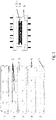
- Laminates 1.1, 1.2, .... 1.5 shown made of polycarbonate each have a constant layer thickness of 0.25 mm. Apertures were formed in the laminates by laser ablation. The openings in the laminate 1.2, which forms the second laminate from the top in the assembled stack, the arc-shaped openings are designed as channels 2 in which cells can be cultivated or biomolecules can be examined.
- actuators or combinations of Sensors with actuators are inserted into an opening and, if necessary, fixed in it.
- electrical feedthroughs 10 vias
- the recesses 5 on the end faces and the positioning holes 5 in the laminates 1.1 to 1.5 can be used for adjustment and positioning before and during the assembly of the system.
- the sensors 4 are inserted into the openings provided for them in the laminates 1.3 and 1.4.
- Electrical conductor tracks 6 are then printed on the surface of the laminate 1.4 in such a way that an electrically conductive connection of the sensors 4 to the outside or to a flexible, deformable circuit board that is not shown here but may be integrated in the laminate stack can be achieved via electrical through-connections (vias) 10 .
- the electrical vias 10 can be filled with an electrically conductive material or openings can be made on the inner walls which are electrically conductively coated and which have also been formed in the laminates.
- FIG 4 the process of sensor embedding and vias 10 fabrication is shown. Joining the laminates 1.4 and 1.5 results in an electrically contacted sensor structure with vias 10, which are designed downwards in order to contact the respective sensor 4 from the underside, for example via elastically deformable, electrically conductive contact elements.
- the sensor 4 itself is embedded between the layers formed with laminates and is in direct contact with the channel 2 and the liquid guided therein.
- the printed electrical contacts 6 of the sensor 4 are sintered under pressure in the hot press 9 at temperatures just below the glass transition temperature of the laminates (1.1, . . . 1.5) in order to achieve improved electrical conductivity.
- Laminate 1.1 shown above has openings for an inflow 7 and an outflow 8.
- a liquid which is a liquid suitable for cultivating living cells and which may contain one or more active substances, can be fed in via the inflow 7 and/or a liquid containing living cells or biomolecules can be introduced.
- the inlets and outlets 7 and 8 are connected to the laminate 1.1 in a fluid-tight and cohesive manner and are arranged in such a way that they are in contact with a front end of a channel 2 which is formed in the laminate 1.2.
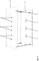
- openings 3 are formed in the sensors 4, not shown here can be used, but as in the figures 2 and 3 is shown.
- the stack thus obtained is inserted into a hot press 9.
- the joining also takes place in several steps, for example in order to figure 4 to generate buried sensor structures shown.
- a thermal treatment was carried out during which the laminates are bonded together at a maximum temperature of 70 °C - 200 °C. This ensures that the liquid contained in the channels 2 cannot escape except from the inflow or outflow 7 or 8 .
- the particles can consist of silver, gold, platinum, copper or alloys thereof, for example.
- an electrochemical sensor for example for measuring the oxygen content
- This consists of 4 laminates 1.10 - 1.14, with the bottom layer 1.14 containing the electrochemical sensor 4, which is analogous to figure 3 is electrically contacted by printed electrical conductors 5.
- laminate 1.13 an introduced microchannel 2, in which there is an electrolyte.
- the electrolyte is separated from the material to be measured in the laminate 1.12 by an inserted membrane 12.
- This membrane 12 is permeable to oxygen but impermeable to the electrolyte and is inserted directly into the composite.
- the laminates 1.11-1.13 contain openings for the electrical contacting of the sensor 4, which can be connected to the peripheral electronics by means of a pin strip 11 in the top laminate 1.11.
- Both the electrolyte and the material to be measured eg culture medium
- Both the electrolyte and the material to be measured can be changed or added in a targeted manner via the fluid inlets 7 and outlets 8 .
- FIG 7 shows figure 7 another embodiment of the invention in the form of a pressure sensor.
- the microchannel 2 is closed at the top by a flexible membrane 13, to which printed structures 5.1 are applied.
- These preferably electrically conductive printed structures 5.1 can be used to implement a strain gauge and thus to measure the membrane deflection or the pressure in the channel 2 by selecting a piezoresistive ink.
Description
Die Erfindung betrifft ein mikrofluidisches System zur Kultivierung von oder der Analyse an lebenden Zellen oder Biomolekülen sowie ein Verfahren zu seiner Herstellung. Dabei können an lebenden Zellen unterschiedlichste Untersuchungen und Einflussmöglichkeiten durchgeführt und überwacht werden. So kann beispielsweise der Einfluss bestimmter Einflussgrößen bzw. Stoffe auf den Stoffwechsel von Zellen detektiert werden. Das System ist auch zur Untersuchung an verschiedenen Biomolekülen, wie z.B. Proteinen, Antikörpern, DNA oder RNA geeignet.The invention relates to a microfluidic system for cultivating or analyzing living cells or biomolecules and a method for its production. A wide variety of examinations and influence options can be carried out and monitored on living cells. For example, the influence of certain influencing factors or Substances on the metabolism of cells can be detected. The system is also suitable for examining various biomolecules such as proteins, antibodies, DNA or RNA.
Für die Zellkultivierung werden aktuell vorrangig polymere Trägermaterialien verwendet. Dies liegt hauptsächlich an der guten Bioverträglichkeit, dem geringen Herstellungspreis (Spritzguss) und der guten optischen Zugänglichkeit begründet. Alle polymerbasierten Systeme haben allerdings das Problem, dass elektrochemische Sensoren z.B. zur Messung des Trans-Epithelialen-Widerstands (TEER) nur extern z.B. in Form von Chopstick-Elektroden eingebracht werden können. Die direkte Implementierung solcher Sensoren würde eine Reihe Vorteile mit sich bringen (Verringerung des Totvolumens, Verbesserung des Messsignals, Reduktion von Kontaminationen, ...). Hier bieten sich keramische Sensoren an, bei denen die elektrochemisch-aktiven Schichten mit einem Siebdruckprozess strukturiert aufgetragen und im Anschluss eingebrannt werden.Polymer carrier materials are currently primarily used for cell cultivation. This is mainly due to the good biocompatibility, the low production price (injection molding) and the good visual accessibility. However, all polymer-based systems have the problem that electrochemical sensors, for example for measuring the trans-epithelial resistance (TEER) can only be introduced externally, for example in the form of chopstick electrodes. The direct implementation of such sensors would bring a number of advantages (reduction of the dead volume, improvement of the measurement signal, reduction of contamination, ...). Ceramic sensors are ideal here, in which the electrochemically active layers are applied in a structured manner using a screen printing process and then burned in.
Die gleichzeitige Realisierung der fluidischen Strukturen in dem Keramiksubstrat, z.B. in LTCC-Technologie ausgeführt, besitzt den entscheidenden Nachteil, dass keramische Substrate optisch nicht transparent und darum für die Zellkultivierung und andere biotechnologische Anwendungen wenig geeignet sind. Überdies lassen sich in mehrlagigen Keramiksubstraten fluidische Aktoren nicht vergleichbar kostengünstig realisieren, wie dies z.B. durch die Integration von flexiblen Elastomermembranen in Polymerverbünden möglich ist.The simultaneous realization of the fluidic structures in the ceramic substrate, e.g. using LTCC technology, has the decisive disadvantage that ceramic substrates are not optically transparent and are therefore not very suitable for cell cultivation and other biotechnological applications. In addition, fluidic actuators cannot be realized in multi-layer ceramic substrates as cost-effectively as is possible, for example, by integrating flexible elastomer membranes in polymer composites.
Weiterhin sind hybride Multilagenaufbauten, wie mehrlagige Leiterplatten mit vergrabenen Bauelementen auf Si- oder Keramiksubstrat bekannt. Dabei werden Multilagenaufbauten auf Polymerträgern verwendet, die andere Materialien umschließen und elektrisch kontaktieren. Gängige Substrate sind Faserverbundwerkstoffe, wie FR-4 oder Polymerfolien, wie Polyimid, auf die Kupferfolie aufkaschiert wird. Diese Materialien besitzen keine oder nur bedingte Bioverträglichkeit oder sind nicht ausreichend transparent und sind darum für den Einsatz in der Zellkultivierung ungeeignet.Furthermore, hybrid multi-layer constructions, such as multi-layer printed circuit boards with buried components on Si or ceramic substrates, are known. Multi-layer structures on polymer carriers are used, which enclose and electrically contact other materials. Common substrates are fiber composites, such as FR-4, or polymer films, such as polyimide, onto which copper foil is laminated. These materials have no or only limited biocompatibility or are not sufficiently transparent and are therefore unsuitable for use in cell cultivation.
Daneben existieren bereits mikrofluidische Systeme, die auch für die Zellkultivierung genutzt werden und eine vergleichsweise hohe Integrationsdichte aufweisen und Sensoren und/oder Aktoren beinhalten. Dabei werden zumeist Glas-Silizium-Hybridsysteme verwendet, wobei sowohl die Strukturierung der mikrofluidischen Kanäle als auch die Herstellung der Sensoren bzw. Aktoren und deren elektrische Kontaktierung zumeist lithografisch erfolgt. Die strukturierten Lagen werden dann bevorzugt mittels anodischem Bonden zu einem fluiddichten Verbund gefügt. Nachteilig an dieser Herstellungstechnologie sind einerseits die hohen Kosten aufgrund der benötigten lithografischen Geräte, der teuren Substratmaterialien und der Masken sowie andererseits die niedrige Fertigungsausbeute, da viele aufwendige Herstellungsschritte nacheinander getätigt werden müssen.In addition, there are already microfluidic systems that are also used for cell cultivation and have a comparatively high integration density and contain sensors and/or actuators. In most cases, glass-silicon hybrid systems are used, with both the structuring of the microfluidic channels and the production of the sensors or actuators and their electrical contacting mostly being carried out lithographically. The structured layers are then joined to form a fluid-tight composite, preferably by means of anodic bonding. Disadvantages of this production technology are on the one hand the high costs due to the required lithographic equipment, the expensive substrate materials and the Masks and, on the other hand, the low production yield, since many complex production steps have to be carried out one after the other.
Eine mikrofluidische Vorrichtung zur Manipulation und Analyse von Fluiden ist in
Es ist daher Aufgabe der Erfindung, Möglichkeiten für eine verbesserte Überwachung und Analyse an lebenden Zellen oder Biomolekülen anzugeben, und gleichzeitig eine gute Biokompatibilität, optische Zugänglichkeit sowie Flexibilität und Kosteneffizienz in der Herstellung einzuhalten.It is therefore the object of the invention to specify possibilities for improved monitoring and analysis of living cells or biomolecules, while at the same time maintaining good biocompatibility, optical accessibility and flexibility and cost-efficiency in production.
Erfindungsgemäß wird diese Aufgabe mit einem mikrofluidischen System, das die Merkmale des Anspruchs 1 aufweist, gelöst. Ein Herstellungsverfahren für ein solches System ist mit dem Anspruch 9 definiert. Vorteilhafte Ausgestaltungen und Weiterbildungen der Erfindung können mit in untergeordneten Ansprüchen bezeichneten Merkmalen realisiert werden.According to the invention, this object is achieved with a microfluidic system that has the features of claim 1 . Claim 9 defines a manufacturing method for such a system. Advantageous refinements and developments of the invention can be realized with the features specified in the subordinate claims.
Bei dem System zur Kultivierung von oder die Analyse an lebenden Zellen oder Biomolekülen sind mehrere übereinander angeordnete Laminate aus einem polymeren Werkstoff fluiddicht und stoffschlüssig miteinander verbunden. Das dafür eingesetzte Polymer sollte bevorzugt optisch transparent sein.In the system for cultivating or analyzing living cells or biomolecules, several laminates made of a polymeric material arranged one above the other are connected to one another in a fluid-tight and cohesive manner. The polymer used for this should preferably be optically transparent.
Erfindungsgemäß ist in einem der Laminate mindestens eine Offnung oder mindestens ein Ausschnitt ausgebildet, mit der/dem ein Kanal oder ein Reservoir für die Aufnahme lebender Zellen oder Biomoleküle ausgebildet ist. Außerdem ist in mindestens einem der Laminate mindestens eine weitere Öffnung ausgebildet, in die ein aus einem keramischen oder einem halbleitenden Werkstoff gebildeter Aktor und/oder Sensor oder ein aus einem keramischen oder halbleitenden Werkstoff gebildeter Träger für einen Aktor oder Sensor eingesetzt ist. Ein Aktor und/oder Sensor sollte dabei so angeordnet und ausgebildet sein, dass ein Kontakt mit einer Flüssigkeit, in der lebende Zellen oder Biomoleküle enthalten sind, oder ein direkter Kontakt mit lebenden Zellen oder Biomolekülen möglich ist. Mindestens ein Aktor und/oder Sensor steht also in berührendem Kontakt mit einer Flüssigkeit für die Kultivierung von Zellen, einer Flüssigkeit in der Biomoleküle enthalten sind oder den in einem Kanal oder Reservoir enthaltenen Zellen oder Biomolekülen.According to the invention, at least one opening or at least one cutout is formed in one of the laminates, with which a channel or a reservoir for receiving living cells or biomolecules is formed. Besides is at least one further opening is formed in at least one of the laminates, into which an actuator and/or sensor made of a ceramic or a semiconducting material or a carrier for an actuator or sensor made of a ceramic or semiconducting material is inserted. An actuator and/or sensor should be arranged and designed in such a way that contact with a liquid containing living cells or biomolecules or direct contact with living cells or biomolecules is possible. At least one actuator and/or sensor is therefore in touching contact with a liquid for the cultivation of cells, a liquid containing biomolecules or the cells or biomolecules contained in a channel or reservoir.
Auf der Oberfläche des Laminats in das der Aktor und/oder Sensor oder der Träger eingesetzt ist oder auf der Oberfläche eines unmittelbar an dieses Laminat angrenzenden Laminats ist mindestens eine elektrische Leiterbahn gedruckt, mit der eine elektrische Kontaktierung des Aktors und/oder Sensors erreichbar ist. Dies kann auch durch Überdrucken der Anschlusskontakte des Sensors/Aktors oder durch das mechanische Andrücken des selbigen an den gedruckten Leiterzug erfolgen.On the surface of the laminate in which the actuator and / or sensor or Carrier is used or on the surface of a laminate immediately adjacent to this laminate at least one electrical conductor track is printed, with which an electrical contact of the actuator and / or sensor can be achieved. This can also be done by overprinting the connection contacts of the sensor/actuator or by mechanically pressing the same onto the printed circuit board.
Ein Aktor und/oder Sensor kann/können auf einer Oberfläche eines Trägers oder in einem Träger angeordnet sein. Als keramische Werkstoffe können beispielsweise LTCC, HTCC oder monolithische Materialien wie Aluminiumoxid, Zirkonoxid, Siliziumnitrid oder Aluminiumnitrid verwendet werden. Als halbleitenden Werkstoff kann Silizium in undotierter oder dotierter Form oder Siliziumdioxid eingesetzt werden.An actuator and/or sensor can be arranged on a surface of a carrier or in a carrier. For example, LTCC, HTCC or monolithic materials such as aluminum oxide, zirconium oxide, silicon nitride or aluminum nitride can be used as ceramic materials. Silicon in undoped or doped form or silicon dioxide can be used as the semiconducting material.
Die Laminate sind erfindungsgemäß Folien und/oder plattenförmige Werkstücke. Die Laminate, welche ein System bilden, sollten möglichst aus dem gleichen Werkstoff bestehen oder zumindest aus sehr ähnlichen polymeren Werkstoffen bestehen, was insbesondere die Glasübergangstemperatur betrifft.According to the invention, the laminates are foils and/or panel-shaped workpieces. The laminates that form a system should, if possible, consist of the same material or at least consist of very similar polymeric materials, which particularly relates to the glass transition temperature.
In mindestens einem der Laminate kann mindestens eine elektrische Durchkontaktierung, bei der in einer Öffnung ein elektrisch leitender Werkstoff enthalten ist, vorhanden sein. Es besteht aber auch die Möglichkeit, ein elastisch verformbares elektrisch leitendes Kontaktelement in eine solche Öffnung einzusetzen. Ein elastisch verformbares Kontaktelement kann aus einem Edelmetall, insbesondere Gold bestehen oder damit beschichtet sein.In at least one of the laminates there can be at least one electrical via, in which an electrically conductive material is contained in an opening. However, there is also the possibility of inserting an elastically deformable, electrically conductive contact element into such an opening. An elastically deformable contact element can consist of a precious metal, in particular gold, or be coated with it.
Die Öffnungen sollten geometrisch so gestaltet und dimensioniert sein, dass ein Aktor und/oder Sensor bzw. ein Träger oder ein elastisch verformbares elektrisch leitendes Element formschlüssig mit einer entsprechenden Ausbildung an dessen Rand gehalten wird.The openings should be designed and dimensioned geometrically in such a way that an actuator and/or sensor or a carrier or an elastically deformable electrically conductive element is held in a form-fitting manner with a corresponding design at its edge.
In einer vorteilhaften Ausführungsform kann zwischen zwei übereinander angeordneten Laminaten eine flexibel verformbare Leiterplatte angeordnet und fluiddicht mit den Laminaten verbunden sein. Die Leiterplatte kann entsprechend mit elektrischen und/oder elektronischen Bauelementen, die über elektrische Leiterbahnen miteinander verbunden sind, bestückt sein. Elektrisch leitende Verbindungen zu einem Aktor bzw. Sensor können über elektrische Durchkontaktierungen (Vias) oder mit elastisch verformbaren elektrisch leitenden Elementen erreicht werden.In an advantageous embodiment, a flexibly deformable printed circuit board can be arranged between two laminates arranged one above the other and connected to the laminates in a fluid-tight manner. The circuit board can accordingly with electrical and / or electronic components that are connected to each other via electrical conductor tracks, be equipped. Electrically conductive connections to an actuator or sensor can be achieved via electrical through-connections (vias) or with elastically deformable electrically conductive elements.
Ein innerhalb des mit den Laminaten gebildeten Stapels angeordneter Sensor kann zur Erfassung physikalischer Größen z.B. Temperatur, Fluss, Volumenstrom, Druck, elektromagnetische Strahlung, elektrische Leitfähigkeit oder der stofflichen Zusammensetzung (z.B. des Sauerstoff-, Glukose- oder Laktatgehalts) genutzt werden oder ein Aktor sein. Aktoren können beispielsweise pneumatisch, thermopneumatisch, elektrostatisch, piezoelektrisch, elektromechanisch angetriebene Membranen oder Kolben sein. Aktoren können auch Elektroden zur elektrischen Zellstimulation, Elektroden zur Zell-/Partikel-Manipulation bzw. -Ablenkung mit Di/Elektrophorese, optoelektronische Komponenten oder piezoelektrische Aktoren sowie Temperierelemente zum Kühlen oder Heizen sein.A sensor arranged within the stack formed with the laminates can be used to record physical quantities, e.g. temperature, flow, volume flow, pressure, electromagnetic radiation, electrical conductivity or the material composition (e.g. the oxygen, glucose or lactate content) or be an actuator . Actuators can be, for example, pneumatically, thermopneumatically, electrostatically, piezoelectrically, electromechanically driven membranes or pistons. Actuators can also be electrodes for electrical cell stimulation, electrodes for cell/particle manipulation or deflection with di/electrophoresis, optoelectronic components or piezoelectric actuators and temperature control elements for cooling or heating.
Im Bereich eines Kanals oder Reservoirs kann mindestens eine permeable Membran, bevorzugt eine gaspermeable Membran angeordnet sein. Damit erschließt sich die Möglichkeit gebildete Gase abzuführen oder eine Gaszufuhr vorzunehmen. So können beispielsweise stoffwechselbedingt gebildete Gase abgeführt und Sauerstoff für die Nährstoffversorgung zugeführt werden. Diese können dann insbesondere was ihre Zusammensetzung und die jeweiligen Volumina betrifft detektiert und ein ggf. aufgetretener Einfluss auf den Stoffwechsel erkannt und nachgeregelt werden. Gaspermeable Membranen können beispielsweise aus Silikonfolien, dünnen Thermoplasten oder thermoplastischen Elastomeren (TPE) gebildet werden. Poröse Membranen (z.B. laserstrukturiere oder track-etched PC-Folie) können z.B. als Zellträger oder zur Herstellung elektrochemischer Sensoren in ein erfindungsgemäßes System integriert sein.At least one permeable membrane, preferably a gas-permeable membrane, can be arranged in the area of a channel or reservoir. This opens up the possibility of discharging formed gases or supplying gas. For example, gases formed as a result of metabolism can be discharged and oxygen can be supplied for the supply of nutrients. These can then be detected, in particular with regard to their composition and the respective volumes, and any influence on the metabolism that may have occurred can be recognized and readjusted. Gas-permeable membranes can be formed from silicone foils, thin thermoplastics or thermoplastic elastomers (TPE), for example. Porous membranes (e.g. laser-structured or track-etched PC film) can be integrated into a system according to the invention, e.g. as cell carriers or for the production of electrochemical sensors.
Ein Kanal oder Reservoir kann mit einer Zu- und/oder Abführung für eine Flüssigkeit, welche lebende Zellen und/oder Biomoleküle enthalten kann, verbunden sein. So kann für eine Zu- oder Abführung jeweils ein Anschlussstutzen durch eine nach außen geführte Öffnung, die in mindestens einem Laminat ausgebildet ist, eingeführt und mit dem jeweiligen Laminat eine fluiddichte und stoffschlüssige Verbindung ausgebildet werden.A channel or reservoir can be connected to an inlet and/or outlet for a liquid which can contain living cells and/or biomolecules. Thus, for an inlet or outlet, a connecting piece can be passed through an outwardly directed opening, which is in at least is formed of a laminate, is introduced and a fluid-tight and materially bonded connection is formed with the respective laminate.
Es besteht auch die Möglichkeit, dass auf mindestens einer Oberfläche mindestens eines Laminats elektrische und/oder elektronische Elemente, insbesondere ein elektrischer Widerstand, ein induktives elektrisches Element, ein kapazitives elektrisches Element oder ein Transistor mittels eines Druckverfahrens ausgebildet sind. Sensorische Elemente, wie z.B. Dehnmessstreifen für die Druckmessung oder Elektrodenstrukturen, z.B. für Partikel- oder Zellmanipulation können mit diesem Verfahren ebenfalls direkt gedruckt werden.There is also the possibility that electrical and/or electronic elements, in particular an electrical resistor, an inductive electrical element, a capacitive electrical element or a transistor, are formed on at least one surface of at least one laminate by means of a printing process. Sensory elements, such as strain gauges for pressure measurement or electrode structures, e.g. for particle or cell manipulation, can also be printed directly using this process.
Ein Kanal oder ein Reservoir kann mit einer semipermeablen Membran an einem Laminat zumindest bereichsweise abgedeckt sein. Die Membran kann dabei für ein Gas permeabel und ggf. für eine Flüssigkeit, wie z.B. einen Elektrolyten impermeabel sein. So kann beispielsweise Sauerstoff oder Kohlendioxid durch die Membran permeieren und in einem auf der anderen Seite der Membran, an der beispielsweise keine Zellkulturen in einer Öffnung vorhanden sind, einem weiteren dort angeordneten Kanal oder Reservoir aber ein geeigneter die jeweilige Gaskonzentration bestimmender Sensor angeordnet sein, mit dem Untersuchungen des Stoffwechsels von Zellkulturen durchgeführt werden können.A channel or a reservoir can be covered at least in regions with a semipermeable membrane on a laminate. The membrane can be permeable to a gas and possibly impermeable to a liquid, such as an electrolyte. For example, oxygen or carbon dioxide can permeate through the membrane and in a further channel or reservoir arranged there on the other side of the membrane, on which, for example, no cell cultures are present in an opening, a suitable sensor determining the respective gas concentration can be arranged with which studies of the metabolism of cell cultures can be carried out.
Ein Kanal oder ein Reservoir kann aber auch mit einer elastisch verformbaren Membran zumindest bereichsweise abgedeckt sein, wobei die Membran mit elektrisch leitenden gedruckten Strukturen, insbesondere Dehnmessstreifen bedruckt sein kann. Damit ist beispielsweise eine Druckmessung im System möglich.However, a channel or a reservoir can also be covered at least in regions with an elastically deformable membrane, in which case the membrane can be imprinted with electrically conductive printed structures, in particular strain gauges. This makes it possible, for example, to measure the pressure in the system.
Ein oder mehrere Membran(en) kann/können beim Fügen der Laminate zwischen benachbarten Laminaten einlaminiert und fluiddicht mit den jeweiligen die Membranoberfläche berührenden Oberflächen der Laminate stoffschlüssig am äußeren Rand der jeweiligen Membran verbunden werden.One or more membrane(s) can be laminated in between adjacent laminates when the laminates are joined and can be cohesively connected to the respective surfaces of the laminates touching the membrane surface in a fluid-tight manner at the outer edge of the respective membrane.
Bei der Herstellung eines erfindungsgemäßen Systems wird so vorgegangen, dass in mindestens einem Laminat, das zwischen einem oberhalb und unterhalb anzuordnenden Laminat angeordnet werden soll, mindestens eine Öffnung oder Aussparung zur Ausbildung eines Kanals oder Reservoirs und in mindestens einem oberhalb oder unterhalb dieses Laminats anzuordnenden Laminats mindestens eine weitere Öffnung zur Aufnahme eines aus keramischen oder halbleitenden Werkstoff gebildeten Aktors und/oder Sensors oder einen Träger eines Aktors und/oder Sensors, der aus einem keramischen oder halbleitenden Werkstoff gebildet ist, ausgebildet werden.In the production of a system according to the invention, the procedure is such that in at least one laminate between an above and is to be arranged underneath the laminate, at least one opening or recess for forming a channel or reservoir and in at least one laminate to be arranged above or below this laminate at least one further opening for receiving an actuator and/or sensor made of ceramic or semiconducting material or a carrier an actuator and/or sensor, which is made of a ceramic or semiconducting material.
In die mindestens eine weitere Öffnung wird ein Aktor und/oder Sensor oder ein Träger eingesetzt. Auf eine Oberfläche dieses Laminats oder eines unmittelbar benachbart anzuordnenden Laminats wird mindestens eine elektrische Leiterbahn für eine elektrische Kontaktierung des Aktors und/oder Sensors mit einem Druckverfahren ausgebildet.An actuator and/or sensor or a carrier is inserted into the at least one further opening. At least one electrical conductor track for electrical contacting of the actuator and/or sensor is formed using a printing process on a surface of this laminate or of a laminate to be arranged directly adjacent.
Die Laminate werden dann so übereinander angeordnet, dass die mindestens eine einen Kanal oder ein Reservoir bildende Öffnung und der mindestens eine Aktor und/oder Sensor zueinander positioniert sind und die den Stapel bildenden Laminate durch eine thermische Behandlung und bevorzugt gleichzeitig wirkenden Druckkräften fluiddicht und stoffschlüssig miteinander verbunden werden.The laminates are then arranged one on top of the other in such a way that the at least one opening forming a channel or a reservoir and the at least one actuator and/or sensor are positioned relative to one another and the laminates forming the stack are fluid-tight and cohesively bonded to one another by thermal treatment and preferably compressive forces acting at the same time get connected.
Die Öffnungen können mittels Stanzen, Prägen, mechanischem Materialabtrag, Laserstrahlschneiden und -ablation oder lithografisch ausgebildet werden.The openings can be formed by stamping, embossing, mechanical material removal, laser beam cutting and ablation, or lithographically.
Mit den Öffnungen oder Aussparungen können Kanäle oder Reservoire mit Abmessungen im Bereich von 10 µm bis 5 mm, was insbesondere deren Höhe und Breite betrifft ausgebildet werden. Ein Kanal kann eine deutlich größere Länge haben und auch nicht ausschließlich entlang einer geradlinigen Längsachse ausgerichtet sein, sondern auch zumindest bereichsweise bogenförmig ausgebildet sein.With the openings or recesses, channels or reservoirs with dimensions in the range from 10 μm to 5 mm, in particular their height and width, can be formed. A channel can have a significantly greater length and also not be aligned exclusively along a straight longitudinal axis, but also be designed in an arc shape at least in some areas.
Das Aufdrucken elektrischer Leiterbahnen und ggf. weiterer elektrischer und/oder elektronischer Bauelemente kann mit direktschreibenden Verfahren (Aerosol-Jet oder Ink-Jet-Druck) von nanopartikelhaltigen Tinten oder mit Siebdruck (polymere Pasten/nanopartikelhaltigen Pasten) erreicht werden. Es können auch gängige Verbindungstechniken, wie z.B. Löten und/oder elastisch verformbare Kontaktelemente zur Herstellung eines elektrischen Kontakts mit peripherer Elektronik verwendet werden.The imprinting of electrical conductor tracks and possibly other electrical and/or electronic components can be achieved with direct-writing methods (aerosol jet or inkjet printing) of inks containing nanoparticles or with screen printing (polymeric pastes/pastes containing nanoparticles). Common connection techniques such as soldering and/or elastically deformable contact elements can also be used to produce an electrical contact with peripheral electronics.
Für das Drucken und auch für die Herstellung elektrisch leitender Durchkontaktierungen können an sich bekannte Pasten oder Suspensionen eingesetzt werden. Diese enthalten elektrisch leitende Partikel, die bei einer thermischen Behandlung miteinander zumindest teilweise versintert werden können. Flüssige und polymere Bestandteile können dabei durch Verdampfen oder durch Sublimation entfernt werden.Known pastes or suspensions can be used for printing and also for the production of electrically conductive plated-through holes. These contain electrically conductive particles which can be at least partially sintered together during a thermal treatment. Liquid and polymeric components can be removed by evaporation or by sublimation.
Mindestens ein Kanal oder mindestens ein Reservoir kann mit Öffnungen oder Aussparungen, die in mehreren benachbart zueinander im Laminatstapel angeordneten Laminaten ausgebildet sind, ausgebildet sein. So können auch dreidimensionale Fluidsysteme über mehrere Lagen ausgebildet werden.At least one channel or at least one reservoir may be formed with openings or recesses formed in a plurality of laminates disposed adjacent one another in the laminate stack. In this way, three-dimensional fluid systems can also be formed over several layers.
Fluidische Strukturen in Form von Kanälen und/oder Reservoiren können nicht nur in Laminaten sondern auch auf einem keramischen oder halbleitenden Werkstoff, wie dies beispielsweise ein Träger sein kann, ausgebildet sein. Diese Strukturen können mit Kanälen und/oder einem Reservoir, die/das im Laminatstapel ausgebildet ist/sind, verbunden sein.Fluidic structures in the form of channels and/or reservoirs can be formed not only in laminates but also on a ceramic or semiconducting material, such as a carrier, for example. These structures may be connected to channels and/or a reservoir formed in the laminate stack.
Mit fluidischen Strukturen können beispielsweise Mikromischer oder Partikelsortierer realisiert werden.Micromixers or particle sorters, for example, can be implemented with fluidic structures.
Aussparungen können bis an den äußeren Rand geführt sein, so dass von dort aus eine Zu- und Abfuhr von Flüssigkeit möglich ist.Recesses can extend to the outer edge so that liquid can be supplied and removed from there.
Für die Laminate können beispielsweise Polycarbonat (PC), Cyclo-Olefine-Copolymer (COC), Polyethylen (PE), Polyethylenterephthalat (PET), Polypropylen (PP), Polystyrol (PS), Polyimid (PI), Polymethylmethacrylat (PMMA), Polyetheretherketon (PEEK), Polytetrafluorethylen (PTFE) oder Silikone, wie z.B. Polydimethylsiloxan (PDMS) und andere Polyorganosiloxane als polymerer Werkstoff eingesetzt werden.For the laminates, for example, polycarbonate (PC), cyclo-olefin copolymer (COC), polyethylene (PE), polyethylene terephthalate (PET), polypropylene (PP), polystyrene (PS), polyimide (PI), polymethyl methacrylate (PMMA), polyetheretherketone (PEEK), polytetrafluoroethylene (PTFE) or silicones such as polydimethylsiloxane (PDMS) and other polyorganosiloxanes are used as polymeric material.
Als Fügetechnologie können thermisches Diffusionsbonden, Plasmafügen, nasschemische Verfahren, laserunterstütztes Fügen, Ultraschallfügen und/oder deren Kombination genutzt werden. Sensoren/Aktoren sollten dabei direkt in den Verbund fluidisch dicht integriert werden können.Thermal diffusion bonding, plasma joining, wet-chemical methods, laser-assisted joining, ultrasonic joining and/or a combination thereof can be used as joining technology. It should be possible to integrate sensors/actuators directly into the network in a fluid-tight manner.
Bei der Erfindung können polymere Basismaterialien verwendet werden, die jeweils einzeln strukturiert, gefügt und bedruckt werden können. Das resultierende System ist weitaus kostengünstiger als Glas-Silizium-basierte Systeme und erlaubt überdies die einfache Implementierung fluidischer Aktoren, wie z.B. Pumpen und Sensoren, wie z.B. Flusssensoren. Mit der beschriebenen Herstellungstechnologie können beliebig viele weitere (auch kommerziell erhältliche) Sensoren/Aktoren auf oder mit einem Keramik- oder Halbleiterwerkstoff erweitert werden. Durch eine veränderte Ausbildung der Laminate mit unterschiedlicher Anordnung und Dimensionierung von Öffnungen können auf einfache Weise unterschiedlich konfigurierte Systeme für verschiedenste Anwendung in entsprechend angepasster Form zur Verfügung gestellt werden.In the invention, polymeric base materials can be used, each of which can be individually structured, joined and printed. The resulting system is far more cost-effective than glass-silicon-based systems and, moreover, allows easy implementation of fluidic actuators, such as pumps, and sensors, such as flow sensors. Any number of other (also commercially available) sensors/actuators can be expanded on or with a ceramic or semiconductor material using the production technology described. By changing the design of the laminates with a different arrangement and dimensioning of openings, differently configured systems for a wide variety of applications can be made available in a correspondingly adapted form in a simple manner.
Es können mikrofluidische Systeme realisiert werden, bei denen mehrlagenkeramische Werkstoffe (LTCC) mit polymeren Werkstoffen (PDMS) über einen Plasma-Aktivierungsprozess der Oberflächen gefügt werden.Microfluidic systems can be realized in which multi-layer ceramic materials (LTCC) are joined with polymeric materials (PDMS) via a plasma activation process of the surfaces.
Mikrofluidische Kanäle und sensorische und/oder aktorisch wirkende Elemente können zusätzlich auch innerhalb des keramischen Werkstoffs realisiert werden. Mehrlagenkeramische Sensoren können innerhalb des jeweiligen polymeren Werkstoffs, mit dem die Laminate gebildet sind, eingebettet und elektrisch kontaktiert werden. Der polymere Werkstoff kann die mikrofluidischen, insbesondere die strömungsmechanischen Funktionen übernehmen.Microfluidic channels and sensory and/or actuatory elements can also be implemented within the ceramic material. Multilayer ceramic sensors can be embedded and electrically contacted within the respective polymeric material with which the laminates are formed. The polymeric material can take over the microfluidic, in particular the flow-mechanical, functions.
Um die Vorteile beider Technologien zu vereinigen, werden keramische Sensoren und/oder Aktoren in polymere, mikrofluidische Multilagensysteme integriert. Dabei kann die optische Zugänglichkeit von außen weitgehend erhalten werden, weil die Sensoren/Aktoren vergleichsweise klein ausgelegt werden können und z.B. mit direktschreibenden Druckverfahren mit niedrigtemperatursinternden nanopartikelhaltigen Tinten elektrisch kontaktierbar bleiben. Dadurch lassen sich mikrofluidische Systeme herstellen, die durch die direkte Implementierung insbesondere elektrischer Sensoren/Aktoren oder auch von optoelektronischen Komponenten eine größere Integrationsdichte und einen größeren Funktionsumfang aufweisen.In order to combine the advantages of both technologies, ceramic sensors and/or actuators are integrated into polymer, microfluidic multi-layer systems. Optical accessibility from the outside can be largely retained because the sensors/actuators can be designed to be comparatively small and, for example, electrically accessible using direct-writing printing processes with low-temperature sintering inks containing nanoparticles remain contactable. This makes it possible to produce microfluidic systems that have a greater integration density and a larger range of functions due to the direct implementation, in particular of electrical sensors/actuators or also of optoelectronic components.
Die Erfindung ermöglicht die Integration verschiedener Sensoren und/oder Aktoren (z.B. elektrochemische Sensoren für die pH-Messung, Elektroden oder Anregungs-LEDs).The invention enables the integration of different sensors and/or actuators (e.g. electrochemical sensors for pH measurement, electrodes or excitation LEDs).
Folgende Fertigungsschritte sollten bei der Herstellung nacheinander durchgeführt werden:
- 1. Herstellung einer Halbschale für die Sensor-/Aktorintegration aus strukturierten Polymerfolien oder -platten, wobei in mindestens einem Laminat Öffnungen zum Einlegen von Aktoren bzw. Sensoren, der Ausbildung mindestens eines Kanals oder Reservoirs vorgesehen sind. Die Strukturierung der Folien kann mechanisch z.B. durch Mikrofräsen, Stanzen, Prägen, oder mittels elektromagnetischer Strahlung bevorzugt mittels Laserablation erfolgen.
- 2. Einlegen der Sensoren/Aktoren in dafür vorgesehene Öffnungen.
- 3. Siegeln und ggf. Abdichten der Sensoren/Aktoren durch z.B. Einkleben, Einlaminieren, Pressen, chemisches Bonden, Ultraschallfügen oder thermisches Bonden und/oder Kombinationen davon.
- 4. Elektrische Kontaktierung der Sensoren/Aktoren mit direktschreibenden Verfahren (Aerosol-Jet oder Ink-Jet-Druck von nanopartikelhaltigen Tinten), Siebdruck (polymere Pasten/ nanopartikelhaltige Pasten)
- 5. Erneutes Fügen/Siegeln der bedruckten Polymerfolien als Laminate mit weiteren strukturierten Polymerfolien oder -platten, um vergrabene elektrische Leiterbahnen herzustellen.
- 6. Durch das Verfüllen von nach oben offenen bzw. vergrabenen Öffnungen, bevorzugt in Form von Löchern, mit elektrisch leitfähigen polymeren Pasten/ nanopartikelhaltigen Pasten können elektrische Durchkontaktierungen generiert werden.
- 7. Die elektrische Kontaktierung mit peripherer Elektronik, z.B. für die Sensor- Signalkonditionierung/Signalverarbeitung, kann direkt durch den Druck kontaktierbarer Anschlusskontakte (Pads), über elastisch verformbare elektrische Kontaktelemente aus einem Edelmetall, insbesondere Gold oder durch die Integration einer lötfähigen FLEX-Leiterplatte (analog zur Integration der Sensoren/Aktoren) erfolgen.
- 8. Zur Herstellung fluidischer und/oder pneumatischer Anschlüsse können verschiedene Konnektoren durch Kleben, Pressen, chemisches Bonden, Laserfügen, Ultraschallfügen oder thermisches Bonden und/oder Kombinationen davon aufgebracht werden und das System in einer Halterung mit pneumatischen und/oder fluidschen Anschlüssen fixiert werden.
- 1. Production of a half-shell for the sensor/actuator integration from structured polymer films or plates, openings for inserting actuators or sensors, the formation of at least one channel or reservoir being provided in at least one laminate. The foils can be structured mechanically, for example by micromilling, punching, embossing, or by means of electromagnetic radiation, preferably by means of laser ablation.
- 2. Inserting the sensors/actuators into the openings provided.
- 3. Sealing and, if necessary, sealing of the sensors/actuators by, for example, gluing, laminating, pressing, chemical bonding, ultrasonic joining or thermal bonding and/or combinations thereof.
- 4. Electrical contacting of the sensors/actuators with direct-writing methods (aerosol jet or ink-jet printing of inks containing nanoparticles), screen printing (polymeric pastes/pastes containing nanoparticles)
- 5. Rejoining/resealing the printed polymer sheets as laminates with other structured polymer sheets or sheets to create buried electrical traces.
- 6. By filling upwardly open or buried openings, preferably in the form of holes, with electrically conductive polymeric pastes/pastes containing nanoparticles, electrical vias can be generated.
- 7. The electrical contacting with peripheral electronics, eg for the sensor signal conditioning/signal processing, can be done directly the pressure of contactable connection contacts (pads), via elastically deformable electrical contact elements made of a precious metal, in particular gold, or by integrating a solderable FLEX printed circuit board (similar to the integration of the sensors/actuators).
- 8. To produce fluidic and/or pneumatic connections, various connectors can be applied by gluing, pressing, chemical bonding, laser joining, ultrasonic joining or thermal bonding and/or combinations thereof and the system can be fixed in a holder with pneumatic and/or fluidic connections.
Der klare Vorteil der beschriebenen Technologie liegt in der Möglichkeit die Vorteile der einzelnen unterschiedlichen Teiltechnologien zu bündeln und dabei die jeweiligen einzelnen Nachteile zu kompensieren. Im Gegensatz zu reinen Multilagen-Keramikaufbauten ist die erfindungsgemäße Hybridtechnologie weitaus kostengünstiger und ressourcenschonender. Es lassen sich mit dieser Technologie Funktionen realisieren, die in polymeren Mikrosystemen ohne weiteres nicht direkt umsetzbar sind. Ein Beispiel dafür sind elektrochemische Sensoren, da für diese keine entsprechenden nanopartikelhaltigen Tinten für den direkten Druck verfügbar sind. Da die optische Zugänglichkeit durch den Einsatz transparenter Folien- oder Plattensubstrate und miniaturisierter Sensoren nur minimal erschwert wird, können die kultivierten Zellen gut beobachtet oder der Zustand oder die Anzahl von Biomolekülen beurteilt bzw. bestimmt und optische Funktionen einfach realisiert werden. So lassen sich zum Beispiel auch auf kleinem Bauraum optische Linsen und andere optische Komponenten mit Detektoren und Anregungs-LEDs o.Ä. kombinieren. Der direkte Druck von Sensoren und Aktoren aber auch von passiven elektrischen Bauelementen, wie elektrischen Widerständen oder Kondensatoren ist mit der Erfindung realisierbar und ermöglicht zukünftig eine Vorverarbeitung der Sensorsignale z.B. zur Temperaturkompensation. Weiterhin bietet die modulare Herstellungstechnologie den Vorteil, dass die einzelnen Komponenten (Sensoren, Aktoren, Substrat mit mikrofluidischen Strukturen) unabhängig voneinander gefertigt und getestet werden können, bevor diese zusammengefügt werden. Dadurch verringert sich die Gesamtausfallswahrscheinlichkeit des Systems und es kann eine Art Baukasten zur Herstellung komplexer mikrofluidischer Systeme zur Verfügung gestellt werden. Elektrische Leiterbahnen können so ausgebildet und betrieben, werden, dass eine elektrische Widerstandsheizung, möglichst in geregelter Form realisiert werden kann. Auch können sensorische und/oder aktorische Elemente direkt gedruckt werden.The clear advantage of the technology described lies in the possibility of bundling the advantages of the individual different sub-technologies and thereby compensating for the respective individual disadvantages. In contrast to purely multi-layer ceramic structures, the hybrid technology according to the invention is far more cost-effective and resource-saving. With this technology, functions can be realized that cannot easily be directly implemented in polymer microsystems. An example of this are electrochemical sensors, as there are no corresponding inks containing nanoparticles available for direct printing. Since optical accessibility is only slightly impeded by the use of transparent film or plate substrates and miniaturized sensors, the cultured cells can be observed well, the condition or the number of biomolecules can be assessed or determined and optical functions can be easily implemented. For example, optical lenses and other optical components can be combined with detectors and excitation LEDs or similar in a small installation space. The direct printing of sensors and actuators, but also of passive electrical components, such as electrical resistors or capacitors, can be realized with the invention and will enable pre-processing of the sensor signals, for example for temperature compensation, in the future. Furthermore, the modular manufacturing technology offers the advantage that the individual components (sensors, actuators, substrate with microfluidic structures) can be manufactured and tested independently of one another before they are assembled. This reduces the Overall failure probability of the system and a kind of construction kit for the production of complex microfluidic systems can be made available. Electrical conductor tracks can be designed and operated in such a way that electrical resistance heating can be implemented, if possible in a controlled manner. Sensory and/or actuatory elements can also be printed directly.
Neben dem zuvor beschriebenen Anwendungsfall bei der Kultivierung humaner Zellen bzw. dem Überwachen der Kultivierungsparameter (Sauerstoff, Glucose, Temperatur, Zellvitalität...) sowie zur Stimulation der Zellen (elektrisch, mechanisch, optisch) gibt es eine Reihe weiterer Anwendungsmöglichkeiten in der Biotechnologie. Diese sind zum Beispiel:
- Die Sortierung von Zellen z.B. mit elektrischen oder magnetischen Feldern,
- der Nachweis oder die Synthese von Biomolekülen (RNA, Antikörper),
- die Einzelzellmanipulation (Fusionierung, Injektion, ...),
- die Umweltanalytik z.B. in Form von Ganzzellsensoren,
- oder spezifische Fragestellungen, wie z.B. on-Chip PCR oder DNA-Hybridisierung.
- The sorting of cells, e.g. with electric or magnetic fields,
- the detection or synthesis of biomolecules (RNA, antibodies),
- single cell manipulation (fusion, injection, ...),
- environmental analysis, e.g. in the form of whole-cell sensors,
- or specific questions such as on-chip PCR or DNA hybridization.
Nachfolgend soll die Erfindung beispielhaft näher erläutert werden.The invention will be explained in more detail below by way of example.
Dabei zeigen:
-
Figur 1 mehrere Laminate in denen jeweils mehrere Öffnungen ausgebildet sind und die zu einem Stapel, bei dem die Laminate übereinander angeordnet sind, mit einer Heißpresse 9 gefügt werden können; -
Figur 2Figur 1 gezeigten Laminate mit Öffnungen in die jeweils ein Sensor eingesetzt wird; -
Figur 3Figur 2 -
Figur 4 -
Figur 5 -
Figur 6 -
Figur 7
-
figure 1 a plurality of laminates in each of which a plurality of openings are formed and which can be joined into a stack in which the laminates are stacked with a hot press 9; -
figure 2 one of the infigure 1 shown laminates with openings in each of which a sensor is used; -
figure 3 this infigure 2 Laminate shown, in which electrical conductor tracks were printed as an electrically conductive connection to the sensors; -
figure 4 two laminates, the lower being the inlaid, printed one contains the sensor and the upper laminate contains vias for electrical contacting and a laminate with a buried electrically contacted sensor is produced by joining in the hot press; -
figure 5 the final assembly of the system by laminating all remaining laminates and applying fluidic connections; -
figure 6 a further exemplary embodiment of an electrochemical sensor with an electrolyte space separated by a membrane and electrodes introduced on a ceramic substrate and -
figure 7 Another embodiment of a pressure sensor printed on a flexible membrane.
Die in
In dem darunter anzuordnenden Laminaten 1.3 und 1.4 sind Öffnungen 3 ausgebildet, in die jeweils ein einem der Kanäle 2 zugeordneter Sensor 4 einsetzbar ist, wie dies auch in
- Formschlüssige Einpassung des
Sensors 4 durch Einbringung einer verformbaren Opferschicht in denSpalt zwischen Sensor 4 und Laminat (z.B. aus einem Thermoplast mit anderen Fließ- und Erweichungseigenschaften) - Übermaßpassung und Ausnutzung der größeren Härte des einzubringenden Sensorsubstrats.
- Einkleben des Sensors in eine Passung mit Spiel.
- Positive fitting of the
sensor 4 by introducing a deformable sacrificial layer into the gap between thesensor 4 and the laminate (e.g. made of a thermoplastic with different flow and softening properties) - Oversize fit and utilization of the greater hardness of the sensor substrate to be introduced.
- Gluing the sensor into a fit with play.
In analoger Form können natürlich auch Aktoren oder Kombinationen von Sensoren mit Aktoren in eine Öffnung eingesetzt und ggf. darin fixiert werden.In analog form, of course, actuators or combinations of Sensors with actuators are inserted into an opening and, if necessary, fixed in it.
Mit weiteren in den anderen Laminaten z.B. 1.5 ausgebildeten Öffnungen können elektrische Durchkontaktierungen 10 (Vias) ausgebildet werden.With further openings formed in the other laminates, e.g. 1.5, electrical feedthroughs 10 (vias) can be formed.
Die Aussparungen 5 an den Stirnseiten, sowie die Positionierungslöcher 5 der Laminate 1.1 bis 1.5 können für eine Justierung und Positionierung vor und während des Fügens des Systems genutzt werden.The
Zunächst werden die Sensoren 4 in die dafür vorgesehenen Öffnungen der Laminate 1.3 und 1.4 eingesetzt. Im Anschluss daran werden elektrische Leiterbahnen 6 auf die Oberfläche des Laminats 1.4 so aufgedruckt, dass eine elektrisch leitende Verbindung der Sensoren 4 nach außen oder zu einer hier nicht gezeigten ggf. aber im Laminatstapel integrierten flexibel verformbaren Leiterplatte über elektrische Durchkontaktierungen (Vias) 10 erreichbar ist. Die elektrischen Durchkontaktierungen 10 können mit einem elektrisch leitenden Werkstoff ausgefüllt oder an den Innenwänden elektrisch leitend beschichteten Öffnungen, die ebenfalls in den Laminaten ausgebildet wurden, hergestellt werden.First, the
In
Bei dem in
Die Zu- und Abflüsse 7 und 8 sind mit dem Laminat 1.1 fluiddicht und stoffschlüssig verbunden und so angeordnet, dass sie mit jeweils einem stirnseitigen Ende eines Kanals 2, der im Laminat 1.2 ausgebildet ist, in Kontakt stehen.The inlets and
Im Laminat 1.3 sind Öffnungen 3 ausgebildet in die hier nicht gezeigte Sensoren 4 einsetzbar sind, wie dies aber in den
Nach dem die Laminate 1.1 bis 1.5 unten und oben des mit den Laminaten 1.2, 1.3 und 1.4 gebildeten Stapels angeordnet und zueinander ausgerichtet sind, wird der so erhaltene Stapel in eine Heißpresse 9 eingesetzt. Je nachdem erfolgt das Fügen auch in mehreren Schritten, um zum Beispiel die in
Während der thermischen Behandlung werden auf den Stapel Druckkräfte mit einem maximalen Druck von 13 MPa ausgeübt.During the thermal treatment, compressive forces with a maximum pressure of 13 MPa are applied to the stack.
Während der thermischen Behandlung erfolgt eine zumindest teilweise Sinterung der Nanopartikel mit denen elektrische Leiterbahnen 6 und ggf. elektrische Durchkontaktierungen 10 ausgebildet wurden. Während der Lamination des Folienstapels wird die Sinterung der Nanopartikel durch die erfolgte Druckbeaufschlagung verstärkt. Die Partikel können beispielsweise aus Silber, Gold, Platin, Kupfer oder Legierungen davon bestehen.During the thermal treatment, at least partial sintering of the nanoparticles takes place, with which electrical conductor tracks 6 and possibly
In
Schließlich zeigt
Claims (11)
- A microfluidic system for culturing or conducting analyses on living cells or biomolecules, in which a plurality of laminates (1.1, 1.2, ..., 1.x), which are arranged on top of one another, made of a polymer material and designed as films and/or panel-shaped workpieces, are joined to one another in a fluid-tight and integral manner, and at least one opening or at least one cut-out is formed in at least one of the laminates (1.1, 1.2, ..., 1.x) by which a channel (2) or a reservoir for receiving living cells or biomolecules is formed, and
at least one further opening (3) is formed in at least one of the laminates (1.1, 1.2, ..., 1.x), into which an actuator and/or a sensor (4) made of a ceramic or semiconducting material, or a carrier for an actuator or a sensor which is made of a ceramic or semiconducting material, is inserted, and at least one electrical strip conductor (6), by way of which electrical contacting of the actuator and/or sensor (4) can be achieved, is printed on the surface of the laminate (1.2) into which the actuator and/or sensor (4) or the carrier is inserted, or on the surface of a laminate (1.3) directly adjoining this laminate (1.2), the at least one actuator and/or sensor (4) being in touching contact with a liquid for the culturing of cells, a liquid in which biomolecules are contained or the cells or biomolecules contained in a channel or reservoir. - The system according to claim 1, characterized in that at least one electrical plated through-hole, in which an electrically conducting material is contained in an opening, and/or an elastically deformable, electrically conducting contact element is inserted in at least one of the laminates (1.1., 1.2, ..., 1.x).
- A system according to any one of the preceding claims, characterized in that a flexibly deformable printed circuit board is arranged between two laminates that are arranged on top of one another and is connected to the laminates in a fluid-tight manner.
- A system according to any one of the preceding claims, characterized in that a sensor (4), arranged within the stack formed by way of the laminates (1.1, 1.2, ..., 1.x), for detecting physical variables, in particular the temperature, the flow, the volume flow rate, the pressure, electromagnetic radiation, the electrical conductivity or the material composition, in particular the oxygen content, glucose content, lactate content, and/or an actuator, in particular a flow source, an electromagnetic radiation-emitting element, an electrode, an actively deformable membrane, a piezo actuator, a gas-permeable membrane, a temperature control element is provided.
- A system according to any one of the preceding claims, characterized in that at least one permeable membrane, preferably a gas-permeable membrane, is arranged in the region of a channel (2) or reservoir.
- A system according to any one of the preceding claims, characterized in that a channel (2) or reservoir is connected to a supply and/or removal device for liquid containing living cells and/or biomolecules.
- A system according to any one of the preceding claims, characterized in that electrical and/or electronic elements, in particular an electrical resistor, a thermocouple, an inductive electrical element, a capacitive electrical element or active components, such as a transistor, are formed on at least one surface of at least one laminate by means of a printing method.
- A system according to any one of the preceding claims, characterized in that a channel (2) or a reservoir is at least partially covered by a semi-permeable membrane (12) on a laminate (1.12)
or
a channel (2) or a reservoir is at least regionally covered by an elastically deformable membrane (13), and the membrane (13) is imprinted with electrically conducting printed structures 5.1, in particular strain gauges. - A method for producing a system according to any one of the preceding claims, characterized in that at least one opening or recess for forming a channel (2) or reservoir is formed in at least one laminate that is to be arranged between a laminate to be arranged above and one to be arranged beneath, andat least one further opening for receiving an actuator and/or a sensor (4) made of a ceramic or semiconducting material, or a carrier of an actuator and/or of a sensor, which is made of a ceramic or semiconducting material, is formed in at least one laminate to be arranged above or beneath this laminate, andan actuator and/or a sensor (4) or a carrier are inserted into the at least one further opening, andat least one electrical strip conductor (6) for electrically contacting the actuator and/or sensor (4) is formed by way of a printing method on a surface of this laminate or of a laminate to be arranged directly adjacent thereto, andthe laminates are arranged stacked on top of one another such that the at least one opening forming a channel (2) or a reservoir and the at least one actuator and/or sensor (4) are positioned facing one another, andthe laminates forming the stack are connected to one another in a fluid-tight and integral manner by way of thermal treatment and simultaneously acting pressure forces, wherein laminates (1.1, 1.2, ..., 1.x) are used which are designed as films and/or panel-shaped workpieces.
- The method according to the preceding claim, characterized in that an electrically conducting plated through-hole, which is formed by electrically conducting material added into the opening, is formed by way of opening formed in at least one laminate, or an elastically deformable, electrically conducting element is inserted into this opening.
- The method according to any one of the two preceding claims, characterized in that at least partial sintering of the material forming the at least one electrical strip conductor and/or the at least one electrical plated through-hole is achieved during the thermal treatment, preferably by way of the action of pressure forces.
Applications Claiming Priority (1)
| Application Number | Priority Date | Filing Date | Title |
|---|---|---|---|
| DE102017205978.8A DE102017205978B4 (en) | 2017-04-07 | 2017-04-07 | Microfluidic system for cultivating or analyzing living cells or biomolecules and a process for its production |
Publications (2)
| Publication Number | Publication Date |
|---|---|
| EP3385367A1 EP3385367A1 (en) | 2018-10-10 |
| EP3385367B1 true EP3385367B1 (en) | 2022-05-04 |
Family
ID=61906758
Family Applications (1)
| Application Number | Title | Priority Date | Filing Date |
|---|---|---|---|
| EP18165888.1A Active EP3385367B1 (en) | 2017-04-07 | 2018-04-05 | Microfluidic system for cultivating or analysing living cells or biomolecules, and a method for its manufacture |
Country Status (2)
| Country | Link |
|---|---|
| EP (1) | EP3385367B1 (en) |
| DE (1) | DE102017205978B4 (en) |
Families Citing this family (1)
| Publication number | Priority date | Publication date | Assignee | Title |
|---|---|---|---|---|
| DE102022113631A1 (en) | 2022-05-31 | 2023-11-30 | Robert Bosch Gesellschaft mit beschränkter Haftung | Analysis system with microfluidic analysis device and microfluidic cartridge |
Family Cites Families (6)
| Publication number | Priority date | Publication date | Assignee | Title |
|---|---|---|---|---|
| US7790443B2 (en) | 2002-08-27 | 2010-09-07 | Vanderbilt University | Bioreactors with substance injection capacity |
| US7419638B2 (en) | 2003-01-14 | 2008-09-02 | Micronics, Inc. | Microfluidic devices for fluid manipulation and analysis |
| DE102007046305A1 (en) | 2007-09-27 | 2009-04-02 | Robert Bosch Gmbh | Microfluidic device and manufacturing method |
| DE102010038445B4 (en) * | 2010-07-27 | 2020-08-27 | Robert Bosch Gmbh | Process for the production of a microfluidic system |
| US9012255B1 (en) | 2010-10-27 | 2015-04-21 | Dunan Microstaq, Inc. | MEMS package |
| DE102012102021A1 (en) * | 2012-03-09 | 2013-09-12 | Epcos Ag | Micromechanical measuring element and method for producing a micromechanical measuring element |
-
2017
- 2017-04-07 DE DE102017205978.8A patent/DE102017205978B4/en not_active Expired - Fee Related
-
2018
- 2018-04-05 EP EP18165888.1A patent/EP3385367B1/en active Active
Also Published As
| Publication number | Publication date |
|---|---|
| DE102017205978A1 (en) | 2018-10-11 |
| DE102017205978B4 (en) | 2021-11-04 |
| EP3385367A1 (en) | 2018-10-10 |
Similar Documents
| Publication | Publication Date | Title |
|---|---|---|
| EP1654065B1 (en) | Flow cell consisting of layers and connection means | |
| DE60105979T2 (en) | METHOD FOR PRODUCING MICROSTRUCTURES WITH DIFFERENT SURFACE PROPERTIES IN A MULTILAYER BODY BY PLASMA SETS | |
| DE19822123C2 (en) | Method and device for the detection of analytes | |
| DE102010002915B4 (en) | Microfluidic sensor | |
| EP1591780B1 (en) | Sensor for detecting fluids, and detection device comprising this sensor | |
| EP2708876B1 (en) | Method for producing a sensor device for detecting chemical or biological species and method for producing a microfluidic device with such a sensor device. | |
| EP2394156B1 (en) | Arrangement and method for electrochemically measuring biochemical reactions and method for producing the arrangement | |
| DE102009023430B4 (en) | Apparatus and method for controlling fluid flows in lab-on-a-chip systems and method of manufacturing the apparatus | |
| EP3143119B1 (en) | Device and method to prepare a biological sample and system for analysis of a biological sample | |
| EP2928606B1 (en) | Manipulation of objects in microfluidic devices using external electrodes | |
| EP1599287A1 (en) | Method and device for contacting a microfluid structure | |
| EP3385367B1 (en) | Microfluidic system for cultivating or analysing living cells or biomolecules, and a method for its manufacture | |
| WO2015169287A1 (en) | Method and devices for the in vitro production of arrangements of cell layers | |
| EP3646029B1 (en) | Detection system and process for its production | |
| EP2522427B1 (en) | Micro-fluid device and method for manufacturing the same | |
| DE19929264A1 (en) | Universal transducer | |
| WO2017129340A1 (en) | Microfluidic flow cell comprising an integrated electrode, and method for manufacturing same | |
| EP3070160A1 (en) | Method and device for processing a sample containing biological material target cells | |
| DE102004062923A1 (en) | Device for conveying fluids, method for producing the same and pipette with such a device | |
| EP1128075A2 (en) | Micropump and/or micromixer with integrated sensor and process for its manufacture | |
| DE10123803C1 (en) | Continuous flow analysis cell, e.g. for detecting glucose, has analysis chamber to which containment which can be filled with reagent is connected by narrow metering channel | |
| WO2001086276A1 (en) | Method for the production of a three-dimensional sensor element | |
| DE10022772C1 (en) | Flow measuring system, used in medical diagnostics, chemical analysis or in biochemical analysis, comprises integrated chemical or biosensor element with plate-like support, channel-like hollow chamber and container | |
| DE102017130198A1 (en) | Analysis arrangement for carrying out biological and / or chemical analyzes of substances and method for its production | |
| WO2004100229A2 (en) | Biocompatible sensor electrode assembly and method for the production thereof |
Legal Events
| Date | Code | Title | Description |
|---|---|---|---|
| PUAI | Public reference made under article 153(3) epc to a published international application that has entered the european phase |
Free format text: ORIGINAL CODE: 0009012 |
|
| STAA | Information on the status of an ep patent application or granted ep patent |
Free format text: STATUS: THE APPLICATION HAS BEEN PUBLISHED |
|
| AK | Designated contracting states |
Kind code of ref document: A1 Designated state(s): AL AT BE BG CH CY CZ DE DK EE ES FI FR GB GR HR HU IE IS IT LI LT LU LV MC MK MT NL NO PL PT RO RS SE SI SK SM TR |
|
| AX | Request for extension of the european patent |
Extension state: BA ME |
|
| STAA | Information on the status of an ep patent application or granted ep patent |
Free format text: STATUS: REQUEST FOR EXAMINATION WAS MADE |
|
| 17P | Request for examination filed |
Effective date: 20190408 |
|
| RBV | Designated contracting states (corrected) |
Designated state(s): AL AT BE BG CH CY CZ DE DK EE ES FI FR GB GR HR HU IE IS IT LI LT LU LV MC MK MT NL NO PL PT RO RS SE SI SK SM TR |
|
| GRAP | Despatch of communication of intention to grant a patent |
Free format text: ORIGINAL CODE: EPIDOSNIGR1 |
|
| STAA | Information on the status of an ep patent application or granted ep patent |
Free format text: STATUS: GRANT OF PATENT IS INTENDED |
|
| INTG | Intention to grant announced |
Effective date: 20211109 |
|
| GRAS | Grant fee paid |
Free format text: ORIGINAL CODE: EPIDOSNIGR3 |
|
| GRAA | (expected) grant |
Free format text: ORIGINAL CODE: 0009210 |
|
| STAA | Information on the status of an ep patent application or granted ep patent |
Free format text: STATUS: THE PATENT HAS BEEN GRANTED |
|
| RAP3 | Party data changed (applicant data changed or rights of an application transferred) |
Owner name: FRAUNHOFER-GESELLSCHAFT ZUR FOERDERUNG DER ANGEWANDTEN FORSCHUNG E.V. |
|
| AK | Designated contracting states |
Kind code of ref document: B1 Designated state(s): AL AT BE BG CH CY CZ DE DK EE ES FI FR GB GR HR HU IE IS IT LI LT LU LV MC MK MT NL NO PL PT RO RS SE SI SK SM TR |
|
| REG | Reference to a national code |
Ref country code: GB Ref legal event code: FG4D Free format text: NOT ENGLISH |
|
| REG | Reference to a national code |
Ref country code: CH Ref legal event code: EP |
|
| REG | Reference to a national code |
Ref country code: AT Ref legal event code: REF Ref document number: 1489084 Country of ref document: AT Kind code of ref document: T Effective date: 20220515 |
|
| REG | Reference to a national code |
Ref country code: DE Ref legal event code: R096 Ref document number: 502018009538 Country of ref document: DE |
|
| REG | Reference to a national code |
Ref country code: IE Ref legal event code: FG4D Free format text: LANGUAGE OF EP DOCUMENT: GERMAN |
|
| REG | Reference to a national code |
Ref country code: LT Ref legal event code: MG9D |
|
| REG | Reference to a national code |
Ref country code: NL Ref legal event code: MP Effective date: 20220504 |
|
| PG25 | Lapsed in a contracting state [announced via postgrant information from national office to epo] |
Ref country code: SE Free format text: LAPSE BECAUSE OF FAILURE TO SUBMIT A TRANSLATION OF THE DESCRIPTION OR TO PAY THE FEE WITHIN THE PRESCRIBED TIME-LIMIT Effective date: 20220504 Ref country code: PT Free format text: LAPSE BECAUSE OF FAILURE TO SUBMIT A TRANSLATION OF THE DESCRIPTION OR TO PAY THE FEE WITHIN THE PRESCRIBED TIME-LIMIT Effective date: 20220905 Ref country code: NO Free format text: LAPSE BECAUSE OF FAILURE TO SUBMIT A TRANSLATION OF THE DESCRIPTION OR TO PAY THE FEE WITHIN THE PRESCRIBED TIME-LIMIT Effective date: 20220804 Ref country code: NL Free format text: LAPSE BECAUSE OF FAILURE TO SUBMIT A TRANSLATION OF THE DESCRIPTION OR TO PAY THE FEE WITHIN THE PRESCRIBED TIME-LIMIT Effective date: 20220504 Ref country code: LT Free format text: LAPSE BECAUSE OF FAILURE TO SUBMIT A TRANSLATION OF THE DESCRIPTION OR TO PAY THE FEE WITHIN THE PRESCRIBED TIME-LIMIT Effective date: 20220504 Ref country code: HR Free format text: LAPSE BECAUSE OF FAILURE TO SUBMIT A TRANSLATION OF THE DESCRIPTION OR TO PAY THE FEE WITHIN THE PRESCRIBED TIME-LIMIT Effective date: 20220504 Ref country code: GR Free format text: LAPSE BECAUSE OF FAILURE TO SUBMIT A TRANSLATION OF THE DESCRIPTION OR TO PAY THE FEE WITHIN THE PRESCRIBED TIME-LIMIT Effective date: 20220805 Ref country code: FI Free format text: LAPSE BECAUSE OF FAILURE TO SUBMIT A TRANSLATION OF THE DESCRIPTION OR TO PAY THE FEE WITHIN THE PRESCRIBED TIME-LIMIT Effective date: 20220504 Ref country code: ES Free format text: LAPSE BECAUSE OF FAILURE TO SUBMIT A TRANSLATION OF THE DESCRIPTION OR TO PAY THE FEE WITHIN THE PRESCRIBED TIME-LIMIT Effective date: 20220504 Ref country code: BG Free format text: LAPSE BECAUSE OF FAILURE TO SUBMIT A TRANSLATION OF THE DESCRIPTION OR TO PAY THE FEE WITHIN THE PRESCRIBED TIME-LIMIT Effective date: 20220804 |
|
| PG25 | Lapsed in a contracting state [announced via postgrant information from national office to epo] |
Ref country code: RS Free format text: LAPSE BECAUSE OF FAILURE TO SUBMIT A TRANSLATION OF THE DESCRIPTION OR TO PAY THE FEE WITHIN THE PRESCRIBED TIME-LIMIT Effective date: 20220504 Ref country code: PL Free format text: LAPSE BECAUSE OF FAILURE TO SUBMIT A TRANSLATION OF THE DESCRIPTION OR TO PAY THE FEE WITHIN THE PRESCRIBED TIME-LIMIT Effective date: 20220504 Ref country code: LV Free format text: LAPSE BECAUSE OF FAILURE TO SUBMIT A TRANSLATION OF THE DESCRIPTION OR TO PAY THE FEE WITHIN THE PRESCRIBED TIME-LIMIT Effective date: 20220504 Ref country code: IS Free format text: LAPSE BECAUSE OF FAILURE TO SUBMIT A TRANSLATION OF THE DESCRIPTION OR TO PAY THE FEE WITHIN THE PRESCRIBED TIME-LIMIT Effective date: 20220904 |
|
| PG25 | Lapsed in a contracting state [announced via postgrant information from national office to epo] |
Ref country code: SM Free format text: LAPSE BECAUSE OF FAILURE TO SUBMIT A TRANSLATION OF THE DESCRIPTION OR TO PAY THE FEE WITHIN THE PRESCRIBED TIME-LIMIT Effective date: 20220504 Ref country code: SK Free format text: LAPSE BECAUSE OF FAILURE TO SUBMIT A TRANSLATION OF THE DESCRIPTION OR TO PAY THE FEE WITHIN THE PRESCRIBED TIME-LIMIT Effective date: 20220504 Ref country code: RO Free format text: LAPSE BECAUSE OF FAILURE TO SUBMIT A TRANSLATION OF THE DESCRIPTION OR TO PAY THE FEE WITHIN THE PRESCRIBED TIME-LIMIT Effective date: 20220504 Ref country code: EE Free format text: LAPSE BECAUSE OF FAILURE TO SUBMIT A TRANSLATION OF THE DESCRIPTION OR TO PAY THE FEE WITHIN THE PRESCRIBED TIME-LIMIT Effective date: 20220504 Ref country code: DK Free format text: LAPSE BECAUSE OF FAILURE TO SUBMIT A TRANSLATION OF THE DESCRIPTION OR TO PAY THE FEE WITHIN THE PRESCRIBED TIME-LIMIT Effective date: 20220504 Ref country code: CZ Free format text: LAPSE BECAUSE OF FAILURE TO SUBMIT A TRANSLATION OF THE DESCRIPTION OR TO PAY THE FEE WITHIN THE PRESCRIBED TIME-LIMIT Effective date: 20220504 |
|
| REG | Reference to a national code |
Ref country code: DE Ref legal event code: R097 Ref document number: 502018009538 Country of ref document: DE |
|
| PLBE | No opposition filed within time limit |
Free format text: ORIGINAL CODE: 0009261 |
|
| STAA | Information on the status of an ep patent application or granted ep patent |
Free format text: STATUS: NO OPPOSITION FILED WITHIN TIME LIMIT |
|
| PG25 | Lapsed in a contracting state [announced via postgrant information from national office to epo] |
Ref country code: AL Free format text: LAPSE BECAUSE OF FAILURE TO SUBMIT A TRANSLATION OF THE DESCRIPTION OR TO PAY THE FEE WITHIN THE PRESCRIBED TIME-LIMIT Effective date: 20220504 |
|
| 26N | No opposition filed |
Effective date: 20230207 |
|
| PG25 | Lapsed in a contracting state [announced via postgrant information from national office to epo] |
Ref country code: SI Free format text: LAPSE BECAUSE OF FAILURE TO SUBMIT A TRANSLATION OF THE DESCRIPTION OR TO PAY THE FEE WITHIN THE PRESCRIBED TIME-LIMIT Effective date: 20220504 |
|
| P01 | Opt-out of the competence of the unified patent court (upc) registered |
Effective date: 20230524 |
|
| PGFP | Annual fee paid to national office [announced via postgrant information from national office to epo] |
Ref country code: DE Payment date: 20230418 Year of fee payment: 6 |
|
| REG | Reference to a national code |
Ref country code: CH Ref legal event code: PL |
|
| GBPC | Gb: european patent ceased through non-payment of renewal fee |
Effective date: 20230405 |
|
| PG25 | Lapsed in a contracting state [announced via postgrant information from national office to epo] |
Ref country code: LU Free format text: LAPSE BECAUSE OF NON-PAYMENT OF DUE FEES Effective date: 20230405 |
|
| REG | Reference to a national code |
Ref country code: BE Ref legal event code: MM Effective date: 20230430 |
|
| PG25 | Lapsed in a contracting state [announced via postgrant information from national office to epo] |
Ref country code: MC Free format text: LAPSE BECAUSE OF FAILURE TO SUBMIT A TRANSLATION OF THE DESCRIPTION OR TO PAY THE FEE WITHIN THE PRESCRIBED TIME-LIMIT Effective date: 20220504 |
|
| PG25 | Lapsed in a contracting state [announced via postgrant information from national office to epo] |
Ref country code: GB Free format text: LAPSE BECAUSE OF NON-PAYMENT OF DUE FEES Effective date: 20230405 |
|
| PG25 | Lapsed in a contracting state [announced via postgrant information from national office to epo] |
Ref country code: MC Free format text: LAPSE BECAUSE OF FAILURE TO SUBMIT A TRANSLATION OF THE DESCRIPTION OR TO PAY THE FEE WITHIN THE PRESCRIBED TIME-LIMIT Effective date: 20220504 Ref country code: LI Free format text: LAPSE BECAUSE OF NON-PAYMENT OF DUE FEES Effective date: 20230430 Ref country code: IT Free format text: LAPSE BECAUSE OF FAILURE TO SUBMIT A TRANSLATION OF THE DESCRIPTION OR TO PAY THE FEE WITHIN THE PRESCRIBED TIME-LIMIT Effective date: 20220504 Ref country code: GB Free format text: LAPSE BECAUSE OF NON-PAYMENT OF DUE FEES Effective date: 20230405 Ref country code: FR Free format text: LAPSE BECAUSE OF NON-PAYMENT OF DUE FEES Effective date: 20230430 Ref country code: CH Free format text: LAPSE BECAUSE OF NON-PAYMENT OF DUE FEES Effective date: 20230430 |
|
| REG | Reference to a national code |
Ref country code: IE Ref legal event code: MM4A |
|
| PG25 | Lapsed in a contracting state [announced via postgrant information from national office to epo] |
Ref country code: BE Free format text: LAPSE BECAUSE OF NON-PAYMENT OF DUE FEES Effective date: 20230430 |
|
| PG25 | Lapsed in a contracting state [announced via postgrant information from national office to epo] |
Ref country code: IE Free format text: LAPSE BECAUSE OF NON-PAYMENT OF DUE FEES Effective date: 20230405 |
|
| PG25 | Lapsed in a contracting state [announced via postgrant information from national office to epo] |
Ref country code: IE Free format text: LAPSE BECAUSE OF NON-PAYMENT OF DUE FEES Effective date: 20230405 |