EP3382852B1 - Ein-/ausschaltvorrichtung und elektronische vorrichtung - Google Patents
Ein-/ausschaltvorrichtung und elektronische vorrichtung Download PDFInfo
- Publication number
- EP3382852B1 EP3382852B1 EP16867956.1A EP16867956A EP3382852B1 EP 3382852 B1 EP3382852 B1 EP 3382852B1 EP 16867956 A EP16867956 A EP 16867956A EP 3382852 B1 EP3382852 B1 EP 3382852B1
- Authority
- EP
- European Patent Office
- Prior art keywords
- pin
- load
- path
- module
- coil
- Prior art date
- Legal status (The legal status is an assumption and is not a legal conclusion. Google has not performed a legal analysis and makes no representation as to the accuracy of the status listed.)
- Active
Links
Images


Classifications
-
- H—ELECTRICITY
- H02—GENERATION; CONVERSION OR DISTRIBUTION OF ELECTRIC POWER
- H02J—ELECTRIC POWER NETWORKS; CIRCUIT ARRANGEMENTS OR SYSTEMS FOR SUPPLYING OR DISTRIBUTING ELECTRIC POWER; SYSTEMS FOR STORING ELECTRIC ENERGY
- H02J50/00—Circuit arrangements or systems for wireless supply or distribution of electric power
- H02J50/20—Circuit arrangements or systems for wireless supply or distribution of electric power using microwaves or radio frequency waves
-
- H—ELECTRICITY
- H02—GENERATION; CONVERSION OR DISTRIBUTION OF ELECTRIC POWER
- H02J—ELECTRIC POWER NETWORKS; CIRCUIT ARRANGEMENTS OR SYSTEMS FOR SUPPLYING OR DISTRIBUTING ELECTRIC POWER; SYSTEMS FOR STORING ELECTRIC ENERGY
- H02J50/00—Circuit arrangements or systems for wireless supply or distribution of electric power
- H02J50/10—Circuit arrangements or systems for wireless supply or distribution of electric power using inductive coupling
- H02J50/12—Circuit arrangements or systems for wireless supply or distribution of electric power using inductive coupling of the resonant type
-
- H—ELECTRICITY
- H04—ELECTRIC COMMUNICATION TECHNIQUE
- H04B—TRANSMISSION
- H04B5/00—Near-field transmission systems, e.g. inductive or capacitive transmission systems
- H04B5/20—Near-field transmission systems, e.g. inductive or capacitive transmission systems characterised by the transmission technique; characterised by the transmission medium
- H04B5/24—Inductive coupling
- H04B5/26—Inductive coupling using coils
-
- H—ELECTRICITY
- H04—ELECTRIC COMMUNICATION TECHNIQUE
- H04B—TRANSMISSION
- H04B5/00—Near-field transmission systems, e.g. inductive or capacitive transmission systems
- H04B5/70—Near-field transmission systems, e.g. inductive or capacitive transmission systems specially adapted for specific purposes
- H04B5/77—Near-field transmission systems, e.g. inductive or capacitive transmission systems specially adapted for specific purposes for interrogation
-
- H—ELECTRICITY
- H04—ELECTRIC COMMUNICATION TECHNIQUE
- H04B—TRANSMISSION
- H04B5/00—Near-field transmission systems, e.g. inductive or capacitive transmission systems
- H04B5/70—Near-field transmission systems, e.g. inductive or capacitive transmission systems specially adapted for specific purposes
- H04B5/79—Near-field transmission systems, e.g. inductive or capacitive transmission systems specially adapted for specific purposes for data transfer in combination with power transfer
Definitions
- Examples of another aspect of the present disclosure provide another on-off apparatus.
- the apparatus includes an AC input port, an AC output port, an on-off module, a first DC isolating component, a second DC isolating component, a third DC isolating component and a fourth DC isolating component.
- the AC input port includes a first end and a second end.
- the AC output port includes a first end and a second end.
- the on-off module includes a first pin, a second pin, a third pin, a fourth pin, a fifth pin, a sixth pin and a control pin.
- the third pin is electrically connected to a DC power supply.
- the fourth pin is connected to a ground end.
- the second unidirectional conduction module is configured to turn on the path between the fifth pin and the sixth pin when the path between the third pin and the fourth pin is turned on, and to turn off the path between the fifth pin and the sixth pin when the path between the third pin and the fourth pin is turned off.
- the switch-on module may be switched on when the on-off module 120 turns on the path between the third pin 123 and the fourth pin 124, and may be switched off when the on-off module 120 turns off the path between the third pin 123 and the fourth pin 124. Therefore the switch-on module may be switched on or off by controlling the path between the third pin 123 and the fourth pin 124 to turn on or off, and the path between the first pin 121 and the second pin 122 may be controlled to turn on or off by the switch-on or switch-off of the switch-on module.
- the control module 128 may include a first connection pin, a second connection pin and a control pin.
- the first connection pin is electrically connected to the third pin 123, and the second connection pin is electrically connected to the first load 126.
- the first connection pin is electrically connected to the second load 127 and the second connection pin is electrically connected to the ground.
- the control pin is configured to receive the control signal and to control connection or disconnection between the first connection pin and the second connection pin under the control of the control signal.
- the resistance value of the first load 126 and the resistance value of the second load 127 may be determined according to the conduction condition of the PIN diode used as the third unidirectional conduction module 129. That is, the resistance value of the first load 126 and the resistance value of the second load 127 satisfy the following conditions. In the case that the path between the third pin 123 and the fourth pin 124 is turned on, the resistance value is maximum when a current in the path between the third pin 123 and the fourth pin 124 is not smaller than the conduction current of the PIN diode used as the third unidirectional conduction module 129.
- Fig. 4 is a schematic diagram of an on-off apparatus provided in this embodiment.
- the on-off apparatus mainly includes an AC input port 400, an AC output port 410, an on-off module 420, a first DC isolating component 430, a second DC isolating component 440, a third DC isolating component 450 and a fourth DC isolating component 460.
- the on-off module 420 may include a first pin 421, a second pin 422, a third pin 423, a fourth pin 424, a fifth pin 425, a sixth pin 426 and a control pin 427.
- the third pin 423 is electrically connected to a DC power supply and the fourth pin 424 is connected to a ground end.
- the first DC isolating component 430 is connected between the first end 401 of the AC input port 400 and the first pin 421.
- the first DC isolating component 430 is configured to isolate a DC signal between the first pin 421 and the first end 401 of the AC input port 400, and to transmit an AC signal between the first pin 421 and the first end 401 of the AC input port 400.
- the first DC isolating component 430 when a path from the DC power supply to the ground is turned on, the DC signal cannot be transmitted through the first DC isolating component 430 to the first end 401 of the AC input port 400. Therefore, functions of the coil may be not influenced.
- the fourth DC isolating component 460 is connected between the second end 412 of the AC output port 410 and the sixth pin 426.
- the fourth DC isolating component 460 is configured to isolate a DC signal between the sixth pin 426 and the second end 412 of the AC output port 410, and to transmit an AC signal between the sixth pin 426 and the second end 412 of the AC output port 410.
- the fourth DC isolating component 460 when the path from the DC power supply to the ground is turned on, the DC signal cannot be transmitted through the fourth DC isolating component 460 to the second end 412 of the AC output port 410. Therefore, communication between the coil and the module behind the AC output port 410 may be not influenced.
- the above on-off apparatus provided in this embodiment may be arranged between the coil of the electronic device and the certain functional module of the electronic device, and may be configured to connect the coil to or disconnect the coil from the certain functional module (such as the chip having the contactless function). Therefore, the functional module may share one coil with another functional module (such as a power acquirement circuit).
- the sixth pin 426 is arranged at a connection point between the third load 4204 and the second unidirectional conduction module 4205, and is connected to the fourth DC isolating component 460.
- the first unidirectional conduction module 4203 is configured to turn on the path between the first pin 421 and the second pin 422 in a case that the path between the third pin 423 and the fourth pin 424 is turned on, and to turn off the path between the first pin 421 and the second pin 422 in a case that the path between the third pin 423 and the fourth pin 424 is turned off.
- the first unidirectional conduction module 4202 has such functions.
- the first unidirectional conduction module 4202 is equivalent to a resistor having a very small resistance value, and the AC signal input at the first end 401 of the AC input port 400 may be transmitted to the first end 411 of the AC output port 410 through the first DC isolating component 430, the first unidirectional conduction module 4202 and the second DC isolating component 440.
- the second unidirectional conduction module 4205 is equivalent to a resistor having a very small resistance value, and the AC signal input at the second end 402 of the AC input port 400 may be transmitted to the second end 412 of the AC output port 410 through the third DC isolating component 450, the second unidirectional conduction module 4205 and the fourth DC isolating component 460.
- the second unidirectional conduction module 4205 is equivalent to a resistor having a very large resistance value and equivalent to a disconnection point, and the AC signal input at the second end 402 of the AC input port 400 cannot be transmitted through the second unidirectional conduction module 4205 to the second end 412 of the AC output port 410. That is, the path from the second end 402 of the AC input port 400 to the second end 412 of the AC output port 410 is turned off.
- the first unidirectional conduction module 4203 may include a second PIN diode.
- the second unidirectional conduction module 4205 may include a third PIN diode. That is, the first unidirectional conduction module 4203 and the second unidirectional conduction module 4205 each may be implemented by the PIN diode.
- the PIN diode has a perfect switch-off characteristic when the PIN diode is switched off. When being switched off, the PIN diode is equivalent to a capacitor of 0.2pF which may block the AC signal between the AC input port 400 and the AC output port 410. That is, the carrier signal from the AC input port 400 to the AC output port 410 is blocked.
- the resistance value of the first load 4201, the resistance value of the second load 4202 and the resistance value of the third load 4204 may be determined according to the conduction condition of the PIN diode used as the first unidirectional conduction module 4203 and the second unidirectional conduction module 4205. That is, the resistance value of the first load 4201, the resistance value of the second load 4202 and the resistance value of the third load 4204 satisfy the following conditions. In the case that the path between the third pin 423 and the fourth pin 424 is turned on, the resistance value is maximum when a current in the path between the third pin 423 and the fourth pin 424 is not smaller than the conduction current of the PIN diode used as the first unidirectional conduction module 4203 and the second unidirectional conduction module 4205.
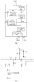
- Fig. 6 is a schematic diagram of a circuit principle of an alternative on-off apparatus provided in this embodiment.
- the first end TA of the AC input port is connected in series to a capacitor C39, a PIN diode D29, a capacitor C40 and the first end LA of the AC output port in sequence.
- An end of a resistor R12 is connected to a connection point between D29 and C40, and another end of the resistor R12 is connected to the DC power supply.
- An end of a resistor R13 is connected to a connection point between C39 and D29, and another end of the resistor R13 is connected to a connection point between the PIN diode D30 and the capacitor C43.
- a negative electrode of the PIN diode D29 is connected to the capacitor C39 and a positive electrode of the PIN diode D29 is connected to the capacitor C40.
- the second end TB of the AC input port is connected in series to a capacitor C41, a PIN diode D30, a capacitor C43 and the second end LB of the AC output port in sequence.
- a negative electrode of the PIN diode D30 is connected to the capacitor C41, and a positive electrode of the PIN diode D30 is connected to the capacitor C43.
- An end of a resistor R16 is connected at a connection point between the capacitor C41 and the PIN diode D30, and another end of the resistor R16 is connected to a D electrode of a NMOS transistor Q8.
- An S electrode of the NMOS transistor Q8 is grounded.
- a G electrode of the NMOS transistor Q8 is connected to the control pin, for receiving the control signal (ANNT_CTRL).
- the NMOS transistor Q8 is switched on or off under the control of the control signal, so as to turn on or off the path form the DC power supply to the ground.
- This embodiment provides an electronic device.
- the electronic device provided in this embodiment may include the on-off apparatus described in any implementation solution of Embodiment 1.
- switch-on or switch-off of an on-off module in the on-off apparatus 74 may be controlled by inputting a control signal, thereby connecting the chip 72 having the contactless function to or disconnecting the chip 72 having the contactless function from the coil 70.
- the electronic device provided in this embodiment may include, but be not limited to, a smart card or an electronic device having a NFC function.
- the electronic device may have functions, such as displaying, inputting or the like.
- the smart card may further include a security chip.
- the security chip may be configured to achieve functions such as electronic signature, signature verification, dynamic password generation and verification or the like.
- the electronic device may communicate with another device (such as a card reader, a POS terminal, a NFC phone or the like) via a wireless manner (such as radio frequency manner, NFC manner or the like).
- the chip having the contactless function may include, but be not limited to, a smart card chip, or an interface chip having the contactless function.
- the interface chip may be connected to a central processing unit (CPU). That is, as long as a chip having the contactless function, the chip may be applicable in this embodiment.
- CPU central processing unit
- the coil 70 may be a radio frequency coil or a NFC coil.
- the coil may operate at 13.56M.
- a signal received by the coil 70 may include, but be not limited to, a contactless signal, such as a NFC signal, a radio frequency signal or the like.
- a non-contact manner refers to a contactless manner which requires no electrical connection for communication.
- the chip 72 having the contactless function may perform a near field communication (NFC) with another device by means of the coil 70 in the contactless manner.
- NFC near field communication
- the chip 72 having the contactless function may be a smart card chip integrated with a microcontroller unit (MCU), and may directly send the control signal to the on-off apparatus 74.
- the chip 72 having the contactless function may also be an interface chip having the contactless function.
- the interface chip may be connected to a CPU, and the CPU sends the control signal to the on-off apparatus 74 through the interface chip. Consequently, the on-off apparatus 74 may be controlled to switch on or switch off by the chip 72 having the contactless function.
- the control signal may also be input to the on-off apparatus 74 through an input device (such as a key) of the electronic device, which is not limited in this embodiment.
- the electronic device may further include a rectifying apparatus 76.
- the rectifying apparatus 76 is electrically connected to the coil 70 and includes an input end and an output end.
- the input end of the rectifying apparatus 76 is electrically connected to the coil 70, for receiving an AC signal output by the coil 70.
- the output end of the rectifying apparatus 76 is configured to output electric energy.
- the rectifying apparatus 76 may share one coil with the chip 72 having the contactless function. By controlling the on-off apparatus 74 to switch on or switch off, the path between the coil 70 and the chip 72 having the contactless function may be turned on or off. Therefore, the coil 70 may provide the electric energy for the rectifying apparatus 76 more effectively.
- the coil 70 is used to communicate with the chip 72 having the contactless function.
- the rectifying apparatus 76 rectifies the AC and outputs the rectified AC for providing a power supply for the electronic device. Therefore, in this embodiment, when the electronic device performs the near field communication with another device, the electronic device may acquire the electric energy from the coil of the electronic device to supply power to the electronic device for working or charging a power supply built-in the electronic device, thereby improving a usage rate of the electronic device.
- the on-off apparatus 74 is connected between the coil 70 and the chip 72 having the contactless function. The on-off apparatus 74 controls the path between the coil 70 and the chip 72 having the contactless function to turn on or off by receiving the control signal.
- the on-off apparatus 74 turns off the path between the coil 70 and the chip 72 having the contactless function. Therefore, the radio frequency carrier between the chip 72 having the contactless function and the coil 70 is turned off. Without the effect of the chip 72 having the contactless function, all of the current of the coil 70 flows into the rectifying apparatus 76 such that the rectifying apparatus 76 may acquire the electric energy at a maximum effectiveness.
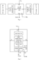
- Fig. 8 is a schematic diagram of an electronic device provided in this embodiment.
- the electronic device provided in this embodiment includes a coil 80, a chip 82 having a contactless function and an on-off apparatus 84 connected between the coil 80 and the chip 82 having the contactless function.
- the coil 80 is connected to an AC input end of the on-off apparatus 84, and the chip 82 having the contactless function is connected to an AC output end of the on-off apparatus 84.
- switch-on and switch-off of an on-off module in the on-off apparatus 84 may be controlled by inputting a control signal, thereby connecting the chip 82 having the contactless function to or disconnecting the chip 82 having the contactless function from the coil 80.
- the electronic device may further include a rectifying apparatus 86.
- the rectifying apparatus 86 is electrically connected to the coil 80, and includes an input end and an output end.
- the input end of the rectifying apparatus 86 is electrically connected to the coil 80, for receiving an AC signal output by the coil 80.
- the output end of the rectifying apparatus 86 is configured to output electric energy.
- the rectifying apparatus 86 may share one coil with the chip 82 having the contactless function. By controlling the on-off apparatus 84 to switch on or switch off, the path between the coil 80 and the chip 82 having the contactless function may be turned on or off. Therefore, the coil 80 may provide the electric energy for the rectifying apparatus 86 more effectively.
- the coil 80 may have two output ends.
- a first output end of the coil 80 is connected respectively to a first input end of the rectifying apparatus 86 and a first end of an AC input end of the on-off apparatus 84.
- a second output end of the coil 80 is connected respectively to a second input end of the rectifying apparatus 86 and a second end of the AC input end of the on-off apparatus 84.
- the first output end and the second output end of the coil 86 output the AC signals having opposite phases.
- a first end of an AC output end of the on-off apparatus 84 is connected to a first end of the chip 82 having the contactless function.
- the electronic device when the electronic device performs the near field communication with another device, the electronic device may acquire the electric energy from the coil of the electronic device to supply power to the electronic device for working or charging a power supply built-in the electronic device, thereby improving a usage rate of the electronic device.
- the on-off apparatus 84 is connected between the coil 80 and the chip 82 having the contactless function.
- the on-off apparatus 84 controls the path between the coil 80 and the chip 82 having the contactless function to turn on or off by receiving the control signal.
- the control signal indicating to turn off the path between the coil 80 and the chip 82 having the contactless function is received, the on-off apparatus 84 turns off the path between the coil 80 and the chip 82 having the contactless function.
- an output end of the rectifying apparatus 86 is connected to another apparatus required to be powered in the electronic device 80, such as a display screen, a key, a security chip or the like, so as to maintain normal operation of another apparatus required to be powered. Therefore, it does not need to provide additional electric energy for another apparatus, thereby saving energy.
- the output end of the rectifying apparatus 86 may be electrically connected to the on-off apparatus 84, for providing the DC power supply for the on-off module of the on-off apparatus 84. That is, the output end of the rectifying apparatus 86 may function as the DC power supply of Embodiment 2.
- the electric energy provided by the coil 80 may be fully used without providing an additional DC power supply for the on-off apparatus 84 separately, thereby saving a size and manufacturing cost of the electronic device.
- the on-off apparatus 84 in this embodiment may adopt any alternative implementation solution described in Embodiment 2.
- Embodiment 2 may be referred to, which is not described in detail in this embodiment.
- the IA end of the diode rectifying bridge in the chip 82 is connected to the first end LA of the AC output end of the on-off apparatus 84, and the IB terminal of the diode rectifying bridge in the chip 82 is connected to the second end LB of the AC output end of the on-off apparatus 84.
- the first output end B of the coil L8 (i.e. an antenna of the electronic device) is connected to the second end TB of the AC input end of the on-off apparatus 84.
- the second output end A of the coil L8 is connected to the first end TA of the AC input end of the on-off apparatus 84.
- the second end LB of the AC output end of the on-off apparatus 84 is connected to the input end LB1 of the chip 82 having the contactless function.
- the first end LA of the AC output end of the on-off apparatus 84 is connected to the input end LA1 of the chip 82 having the contactless function.
- the control pin of the on-off apparatus 84 is configured to receive the control signal ANNT_CTRL.
- the on-off apparatus 84 adopts a circuit structure as illustrated in Embodiment 2, Specific connections of components of the on-off apparatus and the principle of the on-off apparatus may be referred to the descriptions made to Fig. 6 in Embodiment 2.
- embodiments of the present disclosure provide the on-off apparatus, the on-off apparatus is arranged between a coil and a chip of a smart card, by turning on or off a path between the DC power supply and the ground via the on-off module, the coil and the chip are connected or disconnected, thereby realizing to connect and disconnect the radio frequency carrier between the coil and the chip.
- the above-mentioned storage medium may be a read-only memory, a magnetic disc, an optical disc, etc.
Landscapes
- Engineering & Computer Science (AREA)
- Computer Networks & Wireless Communication (AREA)
- Signal Processing (AREA)
- Power Engineering (AREA)
- Charge And Discharge Circuits For Batteries Or The Like (AREA)
Claims (6)
- Eine elektronische Vorrichtung, die eine Spule (70, 80), einen Chip (72, 82) mit einer kontaktlosen Funktion und eine Ein-Aus-Vorrichtung (74, 84) umfasst, wobei, die Ein-Aus-Vorrichtung (74, 84) einen Wechselstrom (AC)-Eingangsanschluss (400), einen AC-Ausgangsanschluss (410), ein Ein-Aus-Modul (420), eine erste Gleichstrom (DC)-Trennkomponente (430), eine zweite DC-Trennkomponente (440), eine dritte DC-Trennkomponente (450) und eine vierte DC-Trennkomponente (460) umfasst; wobei
der AC-Eingangsanschluss (400) ein erstes Ende (401) und ein zweites Ende (402) aufweist;
der Wechselstrom-Ausgangsanschluss (410) ein erstes Ende (411) und ein zweites Ende (412) aufweist;
das Ein-Aus-Modul (420) einen ersten Stift (421), einen zweiten Stift (422), einen dritten Stift (423), einen vierten Stift (424), einen fünften Stift (425), einen sechsten Stift (426) und einen Steuerstift (427) umfasst;
der dritte Stift (423) ist elektrisch mit einer Gleichstromversorgung verbunden, und der vierte Stift (424) ist mit einem Masseende verbunden;
die erste Gleichstrom-Isolationskomponente (430) zwischen dem ersten Ende (401) des Wechselstrom-Eingangsports (400) und dem ersten Stift (421) angeschlossen ist, und die erste Gleichstrom-Isolationskomponente (430) konfiguriert ist, um ein Gleichstromsignal zwischen dem ersten Stift (421) und dem ersten Ende (401) des Wechselstrom-Eingangsports (400) zu isolieren und ein Wechselstromsignal zwischen dem ersten Stift (421) und dem ersten Ende (401) des Wechselstrom-Eingangsports (400) zu übertragen;
die zweite DC-Isolationskomponente (440) zwischen das erste Ende (411) des AC-Ausgangsports (410) und den zweiten Stift (422) geschaltet ist, und die zweite DC-Isolationskomponente (440) konfiguriert ist, um ein DC-Signal zwischen dem zweiten Stift (422) und dem ersten Ende (411) des AC-Ausgangsports (410) zu isolieren und ein AC-Signal zwischen dem zweiten Stift (422) und dem ersten Ende (411) des AC-Ausgangsports (410) zu übertragen;
die dritte Gleichstrom-Isolationskomponente (450) zwischen dem zweiten Ende (402) des Wechselstrom-Eingangsports (400) und dem fünften Stift (425) angeschlossen ist, und die dritte Gleichstrom-Isolationskomponente (450) konfiguriert ist, um ein Gleichstromsignal zwischen dem fünften Stift (425) und dem zweiten Ende (402) des Wechselstrom-Eingangsports (400) zu isolieren und ein Wechselstromsignal zwischen dem fünften Stift (425) und dem zweiten Ende (402) des Wechselstrom-Eingangsports (400) zu übertragen;
die vierte Gleichstrom-Isolationskomponente (460) zwischen dem zweiten Ende (412) des Wechselstrom-Ausgangsports (410) und dem sechsten Stift (426) angeschlossen ist, und die vierte Gleichstrom-Isolationskomponente (460) konfiguriert ist, um ein Gleichstromsignal zwischen dem sechsten Stift (426) und dem zweiten Ende (412) des Wechselstrom-Ausgangsports (410) zu isolieren und ein Wechselstromsignal zwischen dem sechsten Stift (426) und dem zweiten Ende (412) des Wechselstrom-Ausgangsports (410) zu übertragen;
der Steuerstift (427) konfiguriert ist, um ein Steuersignal zu empfangen;
das Ein/Aus-Modul (420) konfiguriert ist, um einen Pfad zwischen dem dritten Stift (423) und dem vierten Stift (424) unter Steuerung des Steuersignals ein- oder auszuschalten, wenn der Pfad zwischen dem dritten Stift (423) und dem vierten Stift (424) eingeschaltet wird, ein Pfad zwischen dem ersten Stift (421) und dem zweiten Stift (422) eingeschaltet wird und ein Pfad zwischen dem fünften Stift (425) und dem sechsten Stift (426) eingeschaltet wird; wenn der Pfad zwischen dem dritten Stift (423) und dem vierten Stift (424) ausgeschaltet ist, wird der Pfad zwischen dem ersten Stift (421) und dem zweiten Stift (422) ausgeschaltet, und der Pfad zwischen dem fünften Stift (425) und dem sechsten Stift (426) wird ausgeschaltet,
die Spule (70, 80) mit dem Wechselstrom-Eingangsende (oder Port) der Ein-Aus-Vorrichtung (74, 84) verbunden ist und der Chip (72, 82) mit der kontaktlosen Funktion mit dem Wechselstrom-Ausgangsende (oder Port) der Ein-Aus-Vorrichtung (74, 84) verbunden ist,
wobei die elektronische Vorrichtung ferner eine Gleichrichtervorrichtung (76, 86) umfasst, wobei die Gleichrichtervorrichtung (76, 86) elektrisch mit der Spule (70, 80) verbunden ist und ein Eingangsende und ein Ausgangsende umfasst, das Eingangsende der Gleichrichtervorrichtung (76, 86) elektrisch mit der Spule (70, 80) verbunden ist und konfiguriert ist, um ein von der Spule (70, 80) ausgegebenes Wechselstromsignal zu empfangen, und das Ausgangsende der Gleichrichtervorrichtung (76, 86) konfiguriert ist, um elektrische Energie auszugeben, wobei das Ausgangsende der Gleichrichtervorrichtung (76, 86) elektrisch mit der Ein-Aus-Vorrichtung (74, 84) verbunden und so konfiguriert ist, dass es die Gleichstromversorgung für das Ein-Aus-Modul (74, 84) bereitstellt. - Die elektronische Vorrichtung nach Anspruch 1, wobei ferner das Ein-Aus-Modul eine erste Last (4201), eine zweite Last (4202), ein erstes unidirektionales Leitungsmodul (4203), eine dritte Last (4204), ein zweites unidirektionales Leitungsmodul (4205) und ein Steuermodul (4207) umfasst;
wobei das Steuermodul (4206) mit dem Steuerpin (427) verbunden ist und das Steuermodul (4206) zwischen den dritten Pin (423) und die erste Last (4201) geschaltet ist, oder das Steuermodul (4206) zwischen den vierten Pin (424) und die zweite Last (4201) geschaltet ist und konfiguriert ist, um den Pfad zwischen dem dritten Pin (423) und dem vierten Pin (424) unter der Steuerung des Steuersignals ein- oder auszuschalten;
wobei das erste unidirektionale Leitungsmodul (4203) zwischen der ersten Last (4201) und der dritten Last (4204) angeschlossen ist, und das zweite unidirektionale Leitungsmodul (4205) zwischen der dritten Last (4204) und der zweiten Last (4202) angeschlossen ist;
wobei der erste Stift (421) an einem Verbindungspunkt zwischen dem ersten unidirektionalen Leitungsmodul (4203) und der dritten Last (4204) angeordnet ist und mit der ersten DC-Trennkomponente (430) verbunden ist;
wobei der zweite Stift (422) an einem Verbindungspunkt zwischen der ersten Last (4201) und dem ersten unidirektionalen Leitungsmodul (4203) angeordnet ist und mit der zweiten Gleichstrom-Trennkomponente (440) verbunden ist;
wobei der fünfte Stift (425) an einem Verbindungspunkt zwischen der zweiten Last (4202) und dem zweiten unidirektionalen Leitungsmodul (4205) angeordnet ist und mit der dritten Gleichstrom-Trennkomponente (450) verbunden ist;
wobei der sechste Stift (426) an einem Verbindungspunkt zwischen der dritten Last (4204) und dem zweiten unidirektionalen Leitungsmodul (4205) angeordnet ist und mit der vierten Gleichstrom-Trennkomponente (460) verbunden ist;
wobei das erste unidirektionale Leitungsmodul (4203) konfiguriert ist, um den Pfad zwischen dem ersten Stift (421) und dem zweiten Stift (422) einzuschalten, wenn der Pfad zwischen dem dritten Stift (423) und dem vierten Stift (424) eingeschaltet wird, und um den Pfad zwischen dem ersten Stift (421) und dem zweiten Stift (422) auszuschalten, wenn der Pfad zwischen dem dritten Stift (423) und dem vierten Stift (424) ausgeschaltet wird;
wobei ferner das zweite unidirektionale Leitungsmodul (4205) konfiguriert ist, um einen Pfad zwischen dem fünften Stift (425) und dem sechsten Stift (426) einzuschalten, wenn der Pfad zwischen dem dritten Stift (423) und dem vierten Stift (424) eingeschaltet ist, und um den Pfad zwischen dem fünften Stift (425) und dem sechsten Stift (426) auszuschalten, wenn der Pfad zwischen dem dritten Stift (423) und dem vierten Stift (424) ausgeschaltet ist. - Die elektronische Vorrichtung nach Anspruch 2, wobei ferner das erste unidirektionale Leitungsmodul (4203) eine zweite PIN-Diode umfasst; und wobei ferner das zweite unidirektionale Leitungsmodul eine dritte PIN-Diode umfasst.
- Die elektronische Vorrichtung nach Anspruch 2, wobei ferner die erste Last (4201), die zweite Last (4202) und die dritte Last (4203) den gleichen Widerstandswert haben und ein Widerstandswert der ersten Last (4201), wobei ferner ein Widerstandswert der zweiten Last (4202) und ein Widerstandswert der dritten Last (4203) größer als ein vorbestimmter Wert sind.
- Die elektronische Vorrichtung nach Anspruch 3 oder 4, wobei ferner die erste Last (126, 4201) den gleichen Widerstandswert wie die zweite Last (127, 4202) hat und ein Widerstandswert der ersten Last (126, 4201) und wobei ferner ein Widerstandswert der zweiten Last (127, 4202) größer als ein vorbestimmter Wert sind.
- Die elektronische Vorrichtung nach einem der Ansprüche 1 bis 5, ferner mit einer Filterkomponente, wobei ferner ein Ende der Filterkomponente elektrisch mit einem Verbindungspunkt zwischen der Gleichstromversorgung und dem dritten Stift (123, 423) verbunden ist und wobei ferner ein anderes Ende der Filterkomponente mit dem Masseende verbunden ist.
Applications Claiming Priority (2)
| Application Number | Priority Date | Filing Date | Title |
|---|---|---|---|
| CN201510849252.6A CN106558923B (zh) | 2015-11-27 | 2015-11-27 | 一种通断装置及电子设备 |
| PCT/CN2016/106795 WO2017088733A1 (zh) | 2015-11-27 | 2016-11-22 | 一种通断装置及电子设备 |
Publications (3)
| Publication Number | Publication Date |
|---|---|
| EP3382852A1 EP3382852A1 (de) | 2018-10-03 |
| EP3382852A4 EP3382852A4 (de) | 2019-05-22 |
| EP3382852B1 true EP3382852B1 (de) | 2020-07-29 |
Family
ID=58418250
Family Applications (1)
| Application Number | Title | Priority Date | Filing Date |
|---|---|---|---|
| EP16867956.1A Active EP3382852B1 (de) | 2015-11-27 | 2016-11-22 | Ein-/ausschaltvorrichtung und elektronische vorrichtung |
Country Status (5)
| Country | Link |
|---|---|
| US (1) | US10432034B2 (de) |
| EP (1) | EP3382852B1 (de) |
| CN (1) | CN106558923B (de) |
| SG (1) | SG11201804349TA (de) |
| WO (1) | WO2017088733A1 (de) |
Family Cites Families (11)
| Publication number | Priority date | Publication date | Assignee | Title |
|---|---|---|---|---|
| JP2011170525A (ja) | 2010-02-17 | 2011-09-01 | Toshiba Corp | カード基材及びこのカード基材を有するicカード |
| CN102723747A (zh) | 2011-03-30 | 2012-10-10 | 海洋王照明科技股份有限公司 | 一种电池充电电路及照明灯具 |
| CN103384962B (zh) | 2012-03-05 | 2015-06-10 | 华为终端有限公司 | 天线切换电路和无线终端设备 |
| KR101979459B1 (ko) * | 2012-12-03 | 2019-05-16 | 엘에스전선 주식회사 | 무선 전력 전송 시스템, 무선 전력 수신 장치 및 무선 전력 수신 방법 |
| JP6292447B2 (ja) | 2013-06-07 | 2018-03-14 | パナソニックIpマネジメント株式会社 | 送受信切替装置 |
| CN104682541B (zh) | 2013-11-27 | 2019-03-26 | 深圳市海洋王照明工程有限公司 | 一种应急灯控制电路及装置 |
| CN104063739B (zh) | 2014-05-05 | 2017-09-22 | 邓君坪 | 一种基于远程控制的射频卡 |
| CN204347787U (zh) * | 2014-10-24 | 2015-05-20 | 韩璐 | 一种含非接触智能卡功能单元的触摸屏控制芯片 |
| CN204166506U (zh) * | 2014-10-24 | 2015-02-18 | 韩璐 | 一种含非接触智能卡感应线圈的触摸屏 |
| CN104899635B (zh) * | 2015-05-11 | 2018-07-20 | 北京握奇数据系统有限公司 | 一种高频和微波双频天线及智能卡 |
| CN205319804U (zh) * | 2015-11-27 | 2016-06-15 | 天地融科技股份有限公司 | 一种通断装置及电子设备 |
-
2015
- 2015-11-27 CN CN201510849252.6A patent/CN106558923B/zh active Active
-
2016
- 2016-11-22 EP EP16867956.1A patent/EP3382852B1/de active Active
- 2016-11-22 US US15/779,053 patent/US10432034B2/en active Active
- 2016-11-22 SG SG11201804349TA patent/SG11201804349TA/en unknown
- 2016-11-22 WO PCT/CN2016/106795 patent/WO2017088733A1/zh not_active Ceased
Non-Patent Citations (1)
| Title |
|---|
| None * |
Also Published As
| Publication number | Publication date |
|---|---|
| US10432034B2 (en) | 2019-10-01 |
| US20180351413A1 (en) | 2018-12-06 |
| SG11201804349TA (en) | 2018-06-28 |
| EP3382852A4 (de) | 2019-05-22 |
| CN106558923B (zh) | 2019-07-30 |
| EP3382852A1 (de) | 2018-10-03 |
| WO2017088733A1 (zh) | 2017-06-01 |
| CN106558923A (zh) | 2017-04-05 |
Similar Documents
| Publication | Publication Date | Title |
|---|---|---|
| US8489020B2 (en) | NFC communicators implementing coil voltage reduction circuitry | |
| US9473208B2 (en) | Recovering data in a near field communication apparatus | |
| JP2007288718A (ja) | 情報処理端末,icカード,携帯型通信装置,無線通信方法,およびプログラム | |
| JP2008259200A (ja) | 非接触型集積回路をnfc素子に結合するための方法 | |
| US10432268B2 (en) | Contactless communication and contactless charging in a system | |
| EP3258424B1 (de) | Elektronische ausrüstung | |
| EP3382852B1 (de) | Ein-/ausschaltvorrichtung und elektronische vorrichtung | |
| CN205319804U (zh) | 一种通断装置及电子设备 | |
| WO2020052461A1 (zh) | 一种智能卡和智能卡的电源切换电路 | |
| CN106560977B (zh) | 一种通断装置及电子设备 | |
| CA3079768C (en) | Data transmitting circuit and apparatus, and data receiving circuit and apparatus | |
| HK1232678B (zh) | 一种通断装置及电子设备 | |
| HK1232678A (en) | On-off apparatus and electronic device | |
| HK1232678A1 (en) | On-off apparatus and electronic device | |
| CN114844530A (zh) | 无源nfc接口和无源nfc设备 |
Legal Events
| Date | Code | Title | Description |
|---|---|---|---|
| STAA | Information on the status of an ep patent application or granted ep patent |
Free format text: STATUS: THE INTERNATIONAL PUBLICATION HAS BEEN MADE |
|
| PUAI | Public reference made under article 153(3) epc to a published international application that has entered the european phase |
Free format text: ORIGINAL CODE: 0009012 |
|
| STAA | Information on the status of an ep patent application or granted ep patent |
Free format text: STATUS: REQUEST FOR EXAMINATION WAS MADE |
|
| 17P | Request for examination filed |
Effective date: 20180608 |
|
| AK | Designated contracting states |
Kind code of ref document: A1 Designated state(s): AL AT BE BG CH CY CZ DE DK EE ES FI FR GB GR HR HU IE IS IT LI LT LU LV MC MK MT NL NO PL PT RO RS SE SI SK SM TR |
|
| AX | Request for extension of the european patent |
Extension state: BA ME |
|
| DAV | Request for validation of the european patent (deleted) | ||
| DAX | Request for extension of the european patent (deleted) | ||
| REG | Reference to a national code |
Ref country code: DE Ref legal event code: R079 Ref document number: 602016041064 Country of ref document: DE Free format text: PREVIOUS MAIN CLASS: H02J0050200000 Ipc: H04B0005000000 |
|
| A4 | Supplementary search report drawn up and despatched |
Effective date: 20190418 |
|
| RIC1 | Information provided on ipc code assigned before grant |
Ipc: H04B 5/00 20060101AFI20190412BHEP Ipc: G06K 19/077 20060101ALI20190412BHEP Ipc: H02J 50/20 20160101ALI20190412BHEP |
|
| GRAP | Despatch of communication of intention to grant a patent |
Free format text: ORIGINAL CODE: EPIDOSNIGR1 |
|
| STAA | Information on the status of an ep patent application or granted ep patent |
Free format text: STATUS: GRANT OF PATENT IS INTENDED |
|
| INTG | Intention to grant announced |
Effective date: 20200227 |
|
| GRAS | Grant fee paid |
Free format text: ORIGINAL CODE: EPIDOSNIGR3 |
|
| GRAA | (expected) grant |
Free format text: ORIGINAL CODE: 0009210 |
|
| STAA | Information on the status of an ep patent application or granted ep patent |
Free format text: STATUS: THE PATENT HAS BEEN GRANTED |
|
| AK | Designated contracting states |
Kind code of ref document: B1 Designated state(s): AL AT BE BG CH CY CZ DE DK EE ES FI FR GB GR HR HU IE IS IT LI LT LU LV MC MK MT NL NO PL PT RO RS SE SI SK SM TR |
|
| REG | Reference to a national code |
Ref country code: CH Ref legal event code: EP |
|
| REG | Reference to a national code |
Ref country code: AT Ref legal event code: REF Ref document number: 1297014 Country of ref document: AT Kind code of ref document: T Effective date: 20200815 |
|
| REG | Reference to a national code |
Ref country code: IE Ref legal event code: FG4D |
|
| REG | Reference to a national code |
Ref country code: DE Ref legal event code: R096 Ref document number: 602016041064 Country of ref document: DE |
|
| REG | Reference to a national code |
Ref country code: LT Ref legal event code: MG4D |
|
| REG | Reference to a national code |
Ref country code: NL Ref legal event code: MP Effective date: 20200729 |
|
| REG | Reference to a national code |
Ref country code: AT Ref legal event code: MK05 Ref document number: 1297014 Country of ref document: AT Kind code of ref document: T Effective date: 20200729 |
|
| PG25 | Lapsed in a contracting state [announced via postgrant information from national office to epo] |
Ref country code: NO Free format text: LAPSE BECAUSE OF FAILURE TO SUBMIT A TRANSLATION OF THE DESCRIPTION OR TO PAY THE FEE WITHIN THE PRESCRIBED TIME-LIMIT Effective date: 20201029 Ref country code: BG Free format text: LAPSE BECAUSE OF FAILURE TO SUBMIT A TRANSLATION OF THE DESCRIPTION OR TO PAY THE FEE WITHIN THE PRESCRIBED TIME-LIMIT Effective date: 20201029 Ref country code: ES Free format text: LAPSE BECAUSE OF FAILURE TO SUBMIT A TRANSLATION OF THE DESCRIPTION OR TO PAY THE FEE WITHIN THE PRESCRIBED TIME-LIMIT Effective date: 20200729 Ref country code: HR Free format text: LAPSE BECAUSE OF FAILURE TO SUBMIT A TRANSLATION OF THE DESCRIPTION OR TO PAY THE FEE WITHIN THE PRESCRIBED TIME-LIMIT Effective date: 20200729 Ref country code: PT Free format text: LAPSE BECAUSE OF FAILURE TO SUBMIT A TRANSLATION OF THE DESCRIPTION OR TO PAY THE FEE WITHIN THE PRESCRIBED TIME-LIMIT Effective date: 20201130 Ref country code: SE Free format text: LAPSE BECAUSE OF FAILURE TO SUBMIT A TRANSLATION OF THE DESCRIPTION OR TO PAY THE FEE WITHIN THE PRESCRIBED TIME-LIMIT Effective date: 20200729 Ref country code: FI Free format text: LAPSE BECAUSE OF FAILURE TO SUBMIT A TRANSLATION OF THE DESCRIPTION OR TO PAY THE FEE WITHIN THE PRESCRIBED TIME-LIMIT Effective date: 20200729 Ref country code: GR Free format text: LAPSE BECAUSE OF FAILURE TO SUBMIT A TRANSLATION OF THE DESCRIPTION OR TO PAY THE FEE WITHIN THE PRESCRIBED TIME-LIMIT Effective date: 20201030 Ref country code: LT Free format text: LAPSE BECAUSE OF FAILURE TO SUBMIT A TRANSLATION OF THE DESCRIPTION OR TO PAY THE FEE WITHIN THE PRESCRIBED TIME-LIMIT Effective date: 20200729 Ref country code: AT Free format text: LAPSE BECAUSE OF FAILURE TO SUBMIT A TRANSLATION OF THE DESCRIPTION OR TO PAY THE FEE WITHIN THE PRESCRIBED TIME-LIMIT Effective date: 20200729 |
|
| PG25 | Lapsed in a contracting state [announced via postgrant information from national office to epo] |
Ref country code: PL Free format text: LAPSE BECAUSE OF FAILURE TO SUBMIT A TRANSLATION OF THE DESCRIPTION OR TO PAY THE FEE WITHIN THE PRESCRIBED TIME-LIMIT Effective date: 20200729 Ref country code: RS Free format text: LAPSE BECAUSE OF FAILURE TO SUBMIT A TRANSLATION OF THE DESCRIPTION OR TO PAY THE FEE WITHIN THE PRESCRIBED TIME-LIMIT Effective date: 20200729 Ref country code: LV Free format text: LAPSE BECAUSE OF FAILURE TO SUBMIT A TRANSLATION OF THE DESCRIPTION OR TO PAY THE FEE WITHIN THE PRESCRIBED TIME-LIMIT Effective date: 20200729 Ref country code: IS Free format text: LAPSE BECAUSE OF FAILURE TO SUBMIT A TRANSLATION OF THE DESCRIPTION OR TO PAY THE FEE WITHIN THE PRESCRIBED TIME-LIMIT Effective date: 20201129 |
|
| PG25 | Lapsed in a contracting state [announced via postgrant information from national office to epo] |
Ref country code: NL Free format text: LAPSE BECAUSE OF FAILURE TO SUBMIT A TRANSLATION OF THE DESCRIPTION OR TO PAY THE FEE WITHIN THE PRESCRIBED TIME-LIMIT Effective date: 20200729 |
|
| PG25 | Lapsed in a contracting state [announced via postgrant information from national office to epo] |
Ref country code: DK Free format text: LAPSE BECAUSE OF FAILURE TO SUBMIT A TRANSLATION OF THE DESCRIPTION OR TO PAY THE FEE WITHIN THE PRESCRIBED TIME-LIMIT Effective date: 20200729 Ref country code: CZ Free format text: LAPSE BECAUSE OF FAILURE TO SUBMIT A TRANSLATION OF THE DESCRIPTION OR TO PAY THE FEE WITHIN THE PRESCRIBED TIME-LIMIT Effective date: 20200729 Ref country code: RO Free format text: LAPSE BECAUSE OF FAILURE TO SUBMIT A TRANSLATION OF THE DESCRIPTION OR TO PAY THE FEE WITHIN THE PRESCRIBED TIME-LIMIT Effective date: 20200729 Ref country code: EE Free format text: LAPSE BECAUSE OF FAILURE TO SUBMIT A TRANSLATION OF THE DESCRIPTION OR TO PAY THE FEE WITHIN THE PRESCRIBED TIME-LIMIT Effective date: 20200729 Ref country code: IT Free format text: LAPSE BECAUSE OF FAILURE TO SUBMIT A TRANSLATION OF THE DESCRIPTION OR TO PAY THE FEE WITHIN THE PRESCRIBED TIME-LIMIT Effective date: 20200729 Ref country code: SM Free format text: LAPSE BECAUSE OF FAILURE TO SUBMIT A TRANSLATION OF THE DESCRIPTION OR TO PAY THE FEE WITHIN THE PRESCRIBED TIME-LIMIT Effective date: 20200729 |
|
| REG | Reference to a national code |
Ref country code: DE Ref legal event code: R097 Ref document number: 602016041064 Country of ref document: DE |
|
| PG25 | Lapsed in a contracting state [announced via postgrant information from national office to epo] |
Ref country code: AL Free format text: LAPSE BECAUSE OF FAILURE TO SUBMIT A TRANSLATION OF THE DESCRIPTION OR TO PAY THE FEE WITHIN THE PRESCRIBED TIME-LIMIT Effective date: 20200729 |
|
| PLBE | No opposition filed within time limit |
Free format text: ORIGINAL CODE: 0009261 |
|
| STAA | Information on the status of an ep patent application or granted ep patent |
Free format text: STATUS: NO OPPOSITION FILED WITHIN TIME LIMIT |
|
| PG25 | Lapsed in a contracting state [announced via postgrant information from national office to epo] |
Ref country code: MC Free format text: LAPSE BECAUSE OF FAILURE TO SUBMIT A TRANSLATION OF THE DESCRIPTION OR TO PAY THE FEE WITHIN THE PRESCRIBED TIME-LIMIT Effective date: 20200729 Ref country code: SK Free format text: LAPSE BECAUSE OF FAILURE TO SUBMIT A TRANSLATION OF THE DESCRIPTION OR TO PAY THE FEE WITHIN THE PRESCRIBED TIME-LIMIT Effective date: 20200729 |
|
| REG | Reference to a national code |
Ref country code: CH Ref legal event code: PL |
|
| 26N | No opposition filed |
Effective date: 20210430 |
|
| PG25 | Lapsed in a contracting state [announced via postgrant information from national office to epo] |
Ref country code: LU Free format text: LAPSE BECAUSE OF NON-PAYMENT OF DUE FEES Effective date: 20201122 |
|
| REG | Reference to a national code |
Ref country code: BE Ref legal event code: MM Effective date: 20201130 |
|
| PG25 | Lapsed in a contracting state [announced via postgrant information from national office to epo] |
Ref country code: SI Free format text: LAPSE BECAUSE OF FAILURE TO SUBMIT A TRANSLATION OF THE DESCRIPTION OR TO PAY THE FEE WITHIN THE PRESCRIBED TIME-LIMIT Effective date: 20200729 Ref country code: LI Free format text: LAPSE BECAUSE OF NON-PAYMENT OF DUE FEES Effective date: 20201130 Ref country code: CH Free format text: LAPSE BECAUSE OF NON-PAYMENT OF DUE FEES Effective date: 20201130 |
|
| PG25 | Lapsed in a contracting state [announced via postgrant information from national office to epo] |
Ref country code: FR Free format text: LAPSE BECAUSE OF NON-PAYMENT OF DUE FEES Effective date: 20201130 Ref country code: IE Free format text: LAPSE BECAUSE OF NON-PAYMENT OF DUE FEES Effective date: 20201122 |
|
| PG25 | Lapsed in a contracting state [announced via postgrant information from national office to epo] |
Ref country code: TR Free format text: LAPSE BECAUSE OF FAILURE TO SUBMIT A TRANSLATION OF THE DESCRIPTION OR TO PAY THE FEE WITHIN THE PRESCRIBED TIME-LIMIT Effective date: 20200729 Ref country code: MT Free format text: LAPSE BECAUSE OF FAILURE TO SUBMIT A TRANSLATION OF THE DESCRIPTION OR TO PAY THE FEE WITHIN THE PRESCRIBED TIME-LIMIT Effective date: 20200729 Ref country code: CY Free format text: LAPSE BECAUSE OF FAILURE TO SUBMIT A TRANSLATION OF THE DESCRIPTION OR TO PAY THE FEE WITHIN THE PRESCRIBED TIME-LIMIT Effective date: 20200729 |
|
| PG25 | Lapsed in a contracting state [announced via postgrant information from national office to epo] |
Ref country code: MK Free format text: LAPSE BECAUSE OF FAILURE TO SUBMIT A TRANSLATION OF THE DESCRIPTION OR TO PAY THE FEE WITHIN THE PRESCRIBED TIME-LIMIT Effective date: 20200729 |
|
| PG25 | Lapsed in a contracting state [announced via postgrant information from national office to epo] |
Ref country code: BE Free format text: LAPSE BECAUSE OF NON-PAYMENT OF DUE FEES Effective date: 20201130 |
|
| PGFP | Annual fee paid to national office [announced via postgrant information from national office to epo] |
Ref country code: DE Payment date: 20251117 Year of fee payment: 10 |
|
| PGFP | Annual fee paid to national office [announced via postgrant information from national office to epo] |
Ref country code: GB Payment date: 20251126 Year of fee payment: 10 |