EP3382759B1 - Bonding structure, flexible panel with bonding structure and fabricating method therefor - Google Patents
Bonding structure, flexible panel with bonding structure and fabricating method therefor Download PDFInfo
- Publication number
- EP3382759B1 EP3382759B1 EP16887726.4A EP16887726A EP3382759B1 EP 3382759 B1 EP3382759 B1 EP 3382759B1 EP 16887726 A EP16887726 A EP 16887726A EP 3382759 B1 EP3382759 B1 EP 3382759B1
- Authority
- EP
- European Patent Office
- Prior art keywords
- protective layer
- chip
- flexible
- bonding
- around
- Prior art date
- Legal status (The legal status is an assumption and is not a legal conclusion. Google has not performed a legal analysis and makes no representation as to the accuracy of the status listed.)
- Active
Links
Images


Classifications
-
- H—ELECTRICITY
- H10—SEMICONDUCTOR DEVICES; ELECTRIC SOLID-STATE DEVICES NOT OTHERWISE PROVIDED FOR
- H10D—INORGANIC ELECTRIC SEMICONDUCTOR DEVICES
- H10D84/00—Integrated devices formed in or on semiconductor substrates that comprise only semiconducting layers, e.g. on Si wafers or on GaAs-on-Si wafers
- H10D84/01—Manufacture or treatment
-
- G—PHYSICS
- G02—OPTICS
- G02F—OPTICAL DEVICES OR ARRANGEMENTS FOR THE CONTROL OF LIGHT BY MODIFICATION OF THE OPTICAL PROPERTIES OF THE MEDIA OF THE ELEMENTS INVOLVED THEREIN; NON-LINEAR OPTICS; FREQUENCY-CHANGING OF LIGHT; OPTICAL LOGIC ELEMENTS; OPTICAL ANALOGUE/DIGITAL CONVERTERS
- G02F1/00—Devices or arrangements for the control of the intensity, colour, phase, polarisation or direction of light arriving from an independent light source, e.g. switching, gating or modulating; Non-linear optics
- G02F1/01—Devices or arrangements for the control of the intensity, colour, phase, polarisation or direction of light arriving from an independent light source, e.g. switching, gating or modulating; Non-linear optics for the control of the intensity, phase, polarisation or colour
- G02F1/13—Devices or arrangements for the control of the intensity, colour, phase, polarisation or direction of light arriving from an independent light source, e.g. switching, gating or modulating; Non-linear optics for the control of the intensity, phase, polarisation or colour based on liquid crystals, e.g. single liquid crystal display cells
- G02F1/133—Constructional arrangements; Operation of liquid crystal cells; Circuit arrangements
- G02F1/1333—Constructional arrangements; Manufacturing methods
- G02F1/133305—Flexible substrates, e.g. plastics, organic film
-
- G—PHYSICS
- G02—OPTICS
- G02F—OPTICAL DEVICES OR ARRANGEMENTS FOR THE CONTROL OF LIGHT BY MODIFICATION OF THE OPTICAL PROPERTIES OF THE MEDIA OF THE ELEMENTS INVOLVED THEREIN; NON-LINEAR OPTICS; FREQUENCY-CHANGING OF LIGHT; OPTICAL LOGIC ELEMENTS; OPTICAL ANALOGUE/DIGITAL CONVERTERS
- G02F1/00—Devices or arrangements for the control of the intensity, colour, phase, polarisation or direction of light arriving from an independent light source, e.g. switching, gating or modulating; Non-linear optics
- G02F1/01—Devices or arrangements for the control of the intensity, colour, phase, polarisation or direction of light arriving from an independent light source, e.g. switching, gating or modulating; Non-linear optics for the control of the intensity, phase, polarisation or colour
- G02F1/13—Devices or arrangements for the control of the intensity, colour, phase, polarisation or direction of light arriving from an independent light source, e.g. switching, gating or modulating; Non-linear optics for the control of the intensity, phase, polarisation or colour based on liquid crystals, e.g. single liquid crystal display cells
- G02F1/133—Constructional arrangements; Operation of liquid crystal cells; Circuit arrangements
- G02F1/1333—Constructional arrangements; Manufacturing methods
- G02F1/1345—Conductors connecting electrodes to cell terminals
- G02F1/13454—Drivers integrated on the active matrix substrate
-
- G—PHYSICS
- G09—EDUCATION; CRYPTOGRAPHY; DISPLAY; ADVERTISING; SEALS
- G09F—DISPLAYING; ADVERTISING; SIGNS; LABELS OR NAME-PLATES; SEALS
- G09F9/00—Indicating arrangements for variable information in which the information is built-up on a support by selection or combination of individual elements
- G09F9/30—Indicating arrangements for variable information in which the information is built-up on a support by selection or combination of individual elements in which the desired character or characters are formed by combining individual elements
- G09F9/301—Indicating arrangements for variable information in which the information is built-up on a support by selection or combination of individual elements in which the desired character or characters are formed by combining individual elements flexible foldable or roll-able electronic displays, e.g. thin LCD, OLED
-
- H—ELECTRICITY
- H10—SEMICONDUCTOR DEVICES; ELECTRIC SOLID-STATE DEVICES NOT OTHERWISE PROVIDED FOR
- H10D—INORGANIC ELECTRIC SEMICONDUCTOR DEVICES
- H10D86/00—Integrated devices formed in or on insulating or conducting substrates, e.g. formed in silicon-on-insulator [SOI] substrates or on stainless steel or glass substrates
-
- H—ELECTRICITY
- H10—SEMICONDUCTOR DEVICES; ELECTRIC SOLID-STATE DEVICES NOT OTHERWISE PROVIDED FOR
- H10W—GENERIC PACKAGES, INTERCONNECTIONS, CONNECTORS OR OTHER CONSTRUCTIONAL DETAILS OF DEVICES COVERED BY CLASS H10
- H10W74/00—Encapsulations, e.g. protective coatings
- H10W74/10—Encapsulations, e.g. protective coatings characterised by their shape or disposition
- H10W74/111—Encapsulations, e.g. protective coatings characterised by their shape or disposition the semiconductor body being completely enclosed
- H10W74/121—Encapsulations, e.g. protective coatings characterised by their shape or disposition the semiconductor body being completely enclosed by multiple encapsulations, e.g. by a thin protective coating and a thick encapsulation
-
- G—PHYSICS
- G02—OPTICS
- G02F—OPTICAL DEVICES OR ARRANGEMENTS FOR THE CONTROL OF LIGHT BY MODIFICATION OF THE OPTICAL PROPERTIES OF THE MEDIA OF THE ELEMENTS INVOLVED THEREIN; NON-LINEAR OPTICS; FREQUENCY-CHANGING OF LIGHT; OPTICAL LOGIC ELEMENTS; OPTICAL ANALOGUE/DIGITAL CONVERTERS
- G02F2201/00—Constructional arrangements not provided for in groups G02F1/00 - G02F7/00
- G02F2201/50—Protective arrangements
-
- G—PHYSICS
- G02—OPTICS
- G02F—OPTICAL DEVICES OR ARRANGEMENTS FOR THE CONTROL OF LIGHT BY MODIFICATION OF THE OPTICAL PROPERTIES OF THE MEDIA OF THE ELEMENTS INVOLVED THEREIN; NON-LINEAR OPTICS; FREQUENCY-CHANGING OF LIGHT; OPTICAL LOGIC ELEMENTS; OPTICAL ANALOGUE/DIGITAL CONVERTERS
- G02F2202/00—Materials and properties
- G02F2202/02—Materials and properties organic material
- G02F2202/022—Materials and properties organic material polymeric
- G02F2202/023—Materials and properties organic material polymeric curable
Definitions
- the disclosure relates to the technical field of display screen, and in particular to flexible screen with a bonding structure and a manufacturing method of the same.
- a flexible screen In the field of manufacturing a flexible display screen, a flexible screen is quite easily damaged in the manufacturing process due to its own relatively fragile material, therefore in practice, it is usually necessary to attach the flexible screen to a substrate (such as tempered glass) and then perform circuit etching, bonding and other steps, and finally separate the flexible screen from the substrate in a manner of peeling-off.
- a substrate such as tempered glass
- circuit etching, bonding and other steps and finally separate the flexible screen from the substrate in a manner of peeling-off.
- the bonding as an example, elements such as a chip are usually boned in a bonding area on the flexible screen, and a large number of circuits are often distributed around the chip. Therefore, an operation of peeling-off the flexible screen and the substrate must be performed carefully, otherwise a product defective may be caused due to an extremely easy damage of the circuits.
- a substrate A is located under the flexible screen, and since there is an obvious hardness difference between the chip B and the flexible screen C itself in the bonding area, relatively large stress will be generated in the bonding area during the actual peeling-off ( as shown in Figure 1 ), thus stress concentration is formed at a position where the chip B is located at (the area indicated by position D is a stress concentration area), in this way the circuits at this position are easily pulled broken, thereby greatly reducing the peeling-off yield after bonding the flexible screen.
- US2011/267320 A1 discloses a flexible device and a fabricating method thereof.
- the flexible device has a flexible panel, a driver, and a restraining component.
- the flexible panel includes a main region and a driver bonding region outside the main region.
- the driver is electrically connected to the driver bonding region.
- the restraining component is disposed adjacent to the driver bonding region. Rigidity of the restraining component is greater than rigidity of the flexible panel, and coefficient of thermal expansion of the restraining component is smaller than coefficient of thermal expansion of the flexible panel.
- US2008/013030 A1 discloses display device with suppressed occurrence of display unevenness.
- the display device includes a flexible base panel, a display panel mounted on the base panel, and a drive circuit component arranged on periphery of and spaced away from the display panel and mounted on the base panel.
- a deformation suppression member is disposed on the base panel at a predetermined portion between the display panel and the drive circuit component.
- US 2005/206016 A1 discloses a flexible screen comprising a display area and a bonding structure, the bonding structure comprising a bonding area connected to the display area and a chip mounted in the bonding area; wherein a flexible protective layer is arranged in the bonding area and the flexible protective layer surrounds around the chip, the flexible protective layer comprises a first protective layer arranged around the chip in the horizontal direction and a second protective layer arranged at the periphery of the first protective layer in the horizontal direction; an inner side of the first protective layer is attached at peripheral edges of the chip, so that the peripheral edges of the chip are connected to a surface of the flexible screen by the first protective layer, the first protective layer and the second protective layer have different materials and both are flexible materials, the second protective layer is distributed in the bonding area, and covers the peripheral areas of the chip, and the second protective layer is a UV adhesive layer coated at the periphery of the first protective layer.
- the flexible screen and a manufacturing method thereof according to the present invention are as defined in the claims.
- the embodiments of the disclosure provide a bonding structure for a flexible screen, a flexible screen with the bonding structure and a manufacturing method of the same, which aim to improve a technical problem in the prior art which is low peeling-off yield of a bonding area in the flexible screen.
- the disclosure provides a bonding structure for a flexible screen, including a bonding area and a chip mounted in the bonding area, and a flexible protective layer is arranged in the bonding area and the flexible protective layer surrounds around the chip.
- the flexible protective layer comprises a first protective layer arranged around the chip and a second protective layer arranged at the periphery of the first protective layer.
- the first protective layer is a UV adhesive layer coated around the chip
- the second protective layer is a silica gel layer coated at the periphery of the first protective layer, an example not forming part of the present invention but useful for understanding it.
- the first protective layer is a polyimide adhesive layer coated around the chip
- the second protective layer is a UV adhesive layer coated at the periphery of the first protective layer.
- first protective layer is attached around the chip, the second protective layer is joined at the periphery of the first protective layer, and the second protective layer has a thickness smaller than a thickness of the first protective layer.
- the thickness of the flexible protective layer is gradually increased in a direction toward the chip.
- the disclosure also provides a manufacturing method of a bonding structure for a flexible screen, the manufacturing method includes:
- said arranging a flexible protective layer around the chip specifically comprises: coating a UV adhesive layer and irradiating the UV adhesive layer with ultraviolet light to make it cure.
- Said arranging a second protective layer at the periphery of the first protective layer specifically comprises: coating a silica gel layer and distributing the silica gel layer throughout the bonding area located at the periphery of the UV adhesive layer.
- said arranging a flexible protective layer around the chip specifically comprises: coating an adhesive layer made of a single material around the chip, and the thickness of the adhesive layer being gradually increased in a direction toward the chip.
- the following technical effects can be achieved by employing at least one of the technical solutions of the disclosure: by forming the flexible protective layer with different hardness around the chip, the stress generated around the chip during the peeling-off are greatly dispersed, a stress gradient is formed, the stress concentration at the position closely adjacent to the periphery of the chip is avoided, the risk of the circuits around the chip being pulled broken can be reduced, and the peeling-off yield of the flexible screen can be finally increased.
- the embodiment of the disclosure provides a bonding structure for a flexible screen.
- the flexible screen includes a display area 10, a bonding area 11 connected to the display area 10 and a chip 20 mounted in the bonding area.
- a flexible protective layer 30 surrounding around the chip 20 is arranged in the bonding area 11, namely the flexible protective layer 30 surrounds around the chip 20 in the horizontal direction.
- the flexible protective layer 30 includes a first protective layer 31 arranged around the chip 20 in the horizontal direction and a second protective layer 32 arranged at the periphery of the first protective layer 31 in the horizontal direction.
- a material for the first protective layer 31 is different from a material for the second protective layer 32, but both of them are flexible materials, and the first protective layer 31 has a thickness greater than that of the second protective layer 32.
- the bonding area 11 is arranged on the flexible screen for bonding the chip 20.
- the bonding area 11 is located on one side of the flexible screen, and the chip 20 is bonded in the bonding area 11 and mounted on the flexible screen.
- the first protective layer 31 surrounds around the chip 20, and an inner side of the first protective layer 31 is attached at the peripheral edges of the chip 20, so that the peripheral edges of the chip 20 are connected to a surface of the flexible screen by the first protective layer 31.
- the second protective layer 32 is distributed in the bonding area 11, and covers the peripheral areas of the chip 20, and the second protective layer 32 covers the first protective area 31, or instead of covering the first protective layer 31, the second protective layer 32 may be coated directly at the periphery of the first protective layer 31 and joined at the periphery of the first protective layer 31, an example not forming part of the present invention but useful for understanding it. Both ways of which can improve the strength of the bonding area 11 and relieve the stress concentration caused during the peeling-off, which can be selected according to practical requirements.
- a double adhesive layer structure with gradually changing hardness is formed around the chip 20, thus a stress gradient can be formed, so that the stress around the chip 20 is gradually increased in a direction gradually approaching the chip 20, thereby achieving the purpose of dispersing stress and avoiding stress concentration.
- the first protective layer 31 may be employed UV (Ultraviolet Rays) adhesive, which is also referred to as ultraviolet light curing adhesive
- the second protective layer 32 may be employed silica gel.
- the silica gel is coated and joined at the periphery of the UV adhesive, and the silica gel is coated throughout the bonding area 11 located at the periphery of the UV adhesive.
- the embodiment of the present disclosure provides a flexible screen bonding structure.
- the embodiment of the present disclosure provides a bonding structure for a flexible screen.
- the flexible screen includes a display area 10, a bonding area 11 connected to the display area 10 and a chip 20 mounted in the bonding area.
- a flexible protective layer 30 surrounding around the chip 20 is arranged in the bonding area 11, and the flexible protective layer 30 is an adhesive layer made of a single material, which is coated in the bonding area 11 of the flexible screen.
- the thickness of the flexible protective layer 30 is gradually increased in a direction toward the chip 20, as shown in Figure 3 , that is, the thickness of the flexible protective layer 30 at the edges of the bonding area 11 is smaller than the thickness of which at the peripheral edges of the chip 20, as such the flexible protective layer 30 with a gradually changing thickness can form a structure with gradually changing hardness around the chip 20, thereby forming a stress gradient, and achieving the purpose of dispersing stress and avoiding stress concentration.
- the protective layer of the present embodiment is an adhesive layer made of a single material, and a stress gradient can be formed by controlling the thickness of the protective layer. Thus the process flow can be decreased and manufacturing difficulty can be reduced.
- the embodiment of the present disclosure provides a manufacturing method of a bonding structure for a flexible screen, which includes the following steps:
- said "arranging a flexible protective layer around the chip” includes: arranging a first protective layer around the chip, so that the first protective layer is respectively connected to the chip and the surface of the flexible screen; and arranging a second protective layer at the periphery of the first protective layer, and the thickness of the second protective layer is smaller than the thickness of the first protective layer.
- said "arranging a first protective layer” refers to coating a UV adhesive layer and irradiating the UV adhesive layer with ultraviolet light to make it cure.
- Said "arranging a second protective layer” refers to coating a silica gel layer, distributing the silica gel layer throughout the bonding area located at the periphery of the first protective layer and connecting the silica gel layer to the UV adhesive layer.
- the materials for the first protective layer and the second protective layer may also be employed other flexible materials.
- said "arranging a first protective layer” refers to coating a polyimide adhesive layer
- said "arranging a second protective layer” refers to coating a UV adhesive layer, which can also disperse the stress around the chip, the description of which will be omitted here.
- "arranging a flexible protective layer around the chip” in S02 may also be performed in other ways, which may include: coating an adhesive layer made of a single material with gradually changing thickness at the periphery of the chip, and the thickness of the adhesive layer being gradually increased in the direction toward the chip.
- coating an adhesive layer made of a single material with gradually changing thickness at the periphery of the chip and the thickness of the adhesive layer being gradually increased in the direction toward the chip.
- the flexible protective layer 30 (such as the first protective layer 31 and the second protective layer 32) with gradually changing hardness can be formed around the chip in the bonding area 11.
- the stress within the bonding area 11 forms a stress gradient from its periphery to its center by the flexible protective layer 30.
- the stress at the edge of the bonding area 11 is minimum (which is because Moh's hardness is the smallest here), and the stress is gradually increased in the direction toward the chip (which is because Moh's hardness is gradually increased), so that the stress around the chip 20 can be greatly dispersed, and the stress concentration created at the position closely adjacent to the periphery of the chip 20 during the peeling-off is avoided, thereby reducing the risk of the circuits around the chip being pulled broken, and finally increasing the peeling-off yield of the flexible screen.
Landscapes
- Physics & Mathematics (AREA)
- Nonlinear Science (AREA)
- General Physics & Mathematics (AREA)
- Optics & Photonics (AREA)
- Crystallography & Structural Chemistry (AREA)
- Chemical & Material Sciences (AREA)
- Mathematical Physics (AREA)
- Engineering & Computer Science (AREA)
- Theoretical Computer Science (AREA)
- Devices For Indicating Variable Information By Combining Individual Elements (AREA)
- Structures Or Materials For Encapsulating Or Coating Semiconductor Devices Or Solid State Devices (AREA)
- Encapsulation Of And Coatings For Semiconductor Or Solid State Devices (AREA)
- Adhesives Or Adhesive Processes (AREA)
Description
- The disclosure relates to the technical field of display screen, and in particular to flexible screen with a bonding structure and a manufacturing method of the same.
- In the field of manufacturing a flexible display screen, a flexible screen is quite easily damaged in the manufacturing process due to its own relatively fragile material, therefore in practice, it is usually necessary to attach the flexible screen to a substrate (such as tempered glass) and then perform circuit etching, bonding and other steps, and finally separate the flexible screen from the substrate in a manner of peeling-off. Taking the bonding as an example, elements such as a chip are usually boned in a bonding area on the flexible screen, and a large number of circuits are often distributed around the chip. Therefore, an operation of peeling-off the flexible screen and the substrate must be performed carefully, otherwise a product defective may be caused due to an extremely easy damage of the circuits.
- In the prior art, a substrate A is located under the flexible screen, and since there is an obvious hardness difference between the chip B and the flexible screen C itself in the bonding area, relatively large stress will be generated in the bonding area during the actual peeling-off ( as shown in
Figure 1 ), thus stress concentration is formed at a position where the chip B is located at (the area indicated by position D is a stress concentration area), in this way the circuits at this position are easily pulled broken, thereby greatly reducing the peeling-off yield after bonding the flexible screen.US2011/267320 A1 discloses a flexible device and a fabricating method thereof. The flexible device has a flexible panel, a driver, and a restraining component. The flexible panel includes a main region and a driver bonding region outside the main region. The driver is electrically connected to the driver bonding region. The restraining component is disposed adjacent to the driver bonding region. Rigidity of the restraining component is greater than rigidity of the flexible panel, and coefficient of thermal expansion of the restraining component is smaller than coefficient of thermal expansion of the flexible panel.
US2008/013030 A1 discloses display device with suppressed occurrence of display unevenness. The display device includes a flexible base panel, a display panel mounted on the base panel, and a drive circuit component arranged on periphery of and spaced away from the display panel and mounted on the base panel. A deformation suppression member is disposed on the base panel at a predetermined portion between the display panel and the drive circuit component.US 2005/206016 A1 discloses a flexible screen comprising a display area and a bonding structure, the bonding structure comprising a bonding area connected to the display area and a chip mounted in the bonding area; wherein a flexible protective layer is arranged in the bonding area and the flexible protective layer surrounds around the chip, the flexible protective layer comprises a first protective layer arranged around the chip in the horizontal direction and a second protective layer arranged at the periphery of the first protective layer in the horizontal direction; an inner side of the first protective layer is attached at peripheral edges of the chip, so that the peripheral edges of the chip are connected to a surface of the flexible screen by the first protective layer, the first protective layer and the second protective layer have different materials and both are flexible materials, the second protective layer is distributed in the bonding area, and covers the peripheral areas of the chip, and the second protective layer is a UV adhesive layer coated at the periphery of the first protective layer. - The flexible screen and a manufacturing method thereof according to the present invention are as defined in the claims. The embodiments of the disclosure provide a bonding structure for a flexible screen, a flexible screen with the bonding structure and a manufacturing method of the same, which aim to improve a technical problem in the prior art which is low peeling-off yield of a bonding area in the flexible screen.
- In order to solve the technical problem mentioned above, the disclosure provides a bonding structure for a flexible screen, including a bonding area and a chip mounted in the bonding area, and a flexible protective layer is arranged in the bonding area and the flexible protective layer surrounds around the chip.
- Further, the flexible protective layer comprises a first protective layer arranged around the chip and a second protective layer arranged at the periphery of the first protective layer.
- Further, the first protective layer is a UV adhesive layer coated around the chip, and the second protective layer is a silica gel layer coated at the periphery of the first protective layer, an example not forming part of the present invention but useful for understanding it.
- According to the present invention, the first protective layer is a polyimide adhesive layer coated around the chip, and the second protective layer is a UV adhesive layer coated at the periphery of the first protective layer.
- Further, an inner side of the first protective layer is attached around the chip, the second protective layer is joined at the periphery of the first protective layer, and the second protective layer has a thickness smaller than a thickness of the first protective layer.
- Further, in an example not forming part of the present invention but useful for understanding it, the thickness of the flexible protective layer is gradually increased in a direction toward the chip.
- The disclosure also provides a manufacturing method of a bonding structure for a flexible screen, the manufacturing method includes:
- setting a bonding area on a surface of the flexible screen, and bonding a chip in the bonding area; and
- arranging a flexible protective layer around the chip.
- Further, said arranging a flexible protective layer around the chip comprises: arranging a first protective layer around the chip so that the first protective layer is respectively connected to the chip and the flexible screen; and
- arranging a second protective layer at the periphery of the first protective layer, the second protective layer having a thickness smaller than a thickness of the first protective layer.
- Further, in an example not forming part of the present invention but useful for understanding it, said arranging a flexible protective layer around the chip specifically comprises: coating a UV adhesive layer and irradiating the UV adhesive layer with ultraviolet light to make it cure. Said arranging a second protective layer at the periphery of the first protective layer specifically comprises: coating a silica gel layer and distributing the silica gel layer throughout the bonding area located at the periphery of the UV adhesive layer.
- Further, in an example not forming part of the present invention but useful for understanding it, said arranging a flexible protective layer around the chip specifically comprises: coating an adhesive layer made of a single material around the chip, and the thickness of the adhesive layer being gradually increased in a direction toward the chip.
- The following technical effects can be achieved by employing at least one of the technical solutions of the disclosure: by forming the flexible protective layer with different hardness around the chip, the stress generated around the chip during the peeling-off are greatly dispersed, a stress gradient is formed, the stress concentration at the position closely adjacent to the periphery of the chip is avoided, the risk of the circuits around the chip being pulled broken can be reduced, and the peeling-off yield of the flexible screen can be finally increased.
- The illustrated drawings herein are provided for further understanding of the disclosure and constitute a part of the disclosure. The exemplary embodiments of the disclosure and the descriptions thereof aim to explain the disclosure rather than improperly limit the disclosure. In the drawings:
-
Figure 1 is a structural schematic view during a flexible screen being peeled from a substrate in the prior art; -
Figure 2 is a schematic view of a bonding structure for a flexible screen in an embodiment 1 of the disclosure, according to the present invention; -
Figure 3 is a schematic view of a bonding structure for a flexible screen in anembodiment 2 of the disclosure, an example not forming part of the present invention but useful for understanding it; -
Figure 4 is a flow chart of a manufacturing method of a bonding structure for a flexible screen in an embodiment 3 of the disclosure, according to the present invention; -
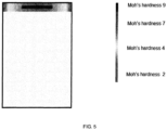
Figure 5 is a hardness distribution view of the bonding structure for the flexible screen in the embodiment 3 of the disclosure, an example not forming part of the present invention but useful for understanding it; - To make objects, technical solutions, and advantages of the disclosure more clear, the technical solutions of the disclosure will be described clearly and completely below in combination with specific embodiments and corresponding accompanying drawings of the disclosure. It is apparent that the described embodiment is only a part of the embodiments of the disclosure, not all the embodiments. On the basis of the embodiments of the disclosure, all other embodiments obtained by a person skilled in the art without paying creative work will fall within the protection scope of the disclosure.
- The technical solutions provided by each embodiment of the disclosure are described in detail below in combination with the accompanying drawings.
- In order to solve the problem of low peeling-off yield of an existing flexible screen, the embodiment of the disclosure provides a bonding structure for a flexible screen. With reference to
Figure 2 , the flexible screen includes adisplay area 10, abonding area 11 connected to thedisplay area 10 and achip 20 mounted in the bonding area. A flexibleprotective layer 30 surrounding around thechip 20 is arranged in thebonding area 11, namely the flexibleprotective layer 30 surrounds around thechip 20 in the horizontal direction. Wherein the flexibleprotective layer 30 includes a firstprotective layer 31 arranged around thechip 20 in the horizontal direction and a secondprotective layer 32 arranged at the periphery of the firstprotective layer 31 in the horizontal direction. A material for the firstprotective layer 31 is different from a material for the secondprotective layer 32, but both of them are flexible materials, and the firstprotective layer 31 has a thickness greater than that of the secondprotective layer 32. - Wherein the
bonding area 11 is arranged on the flexible screen for bonding thechip 20. In the present embodiment, thebonding area 11 is located on one side of the flexible screen, and thechip 20 is bonded in thebonding area 11 and mounted on the flexible screen. The firstprotective layer 31 surrounds around thechip 20, and an inner side of the firstprotective layer 31 is attached at the peripheral edges of thechip 20, so that the peripheral edges of thechip 20 are connected to a surface of the flexible screen by the firstprotective layer 31. The secondprotective layer 32 is distributed in thebonding area 11, and covers the peripheral areas of thechip 20, and the secondprotective layer 32 covers the firstprotective area 31, or instead of covering the firstprotective layer 31, the secondprotective layer 32 may be coated directly at the periphery of the firstprotective layer 31 and joined at the periphery of the firstprotective layer 31, an example not forming part of the present invention but useful for understanding it. Both ways of which can improve the strength of thebonding area 11 and relieve the stress concentration caused during the peeling-off, which can be selected according to practical requirements. By arranging the firstprotective layer 31 and the secondprotective layer 32 with different materials, a double adhesive layer structure with gradually changing hardness is formed around thechip 20, thus a stress gradient can be formed, so that the stress around thechip 20 is gradually increased in a direction gradually approaching thechip 20, thereby achieving the purpose of dispersing stress and avoiding stress concentration. - In an embodiment not forming part of the present invention but useful for understanding it, preferably, the first
protective layer 31 may be employed UV (Ultraviolet Rays) adhesive, which is also referred to as ultraviolet light curing adhesive, and the secondprotective layer 32 may be employed silica gel. The silica gel is coated and joined at the periphery of the UV adhesive, and the silica gel is coated throughout thebonding area 11 located at the periphery of the UV adhesive. - The embodiment of the present disclosure provides a flexible screen bonding structure. The embodiment of the present disclosure provides a bonding structure for a flexible screen. With reference to
Figure 2 , the flexible screen includes adisplay area 10, abonding area 11 connected to thedisplay area 10 and achip 20 mounted in the bonding area. A flexibleprotective layer 30 surrounding around thechip 20 is arranged in thebonding area 11, and the flexibleprotective layer 30 is an adhesive layer made of a single material, which is coated in thebonding area 11 of the flexible screen. The thickness of the flexibleprotective layer 30 is gradually increased in a direction toward thechip 20, as shown inFigure 3 , that is, the thickness of the flexibleprotective layer 30 at the edges of thebonding area 11 is smaller than the thickness of which at the peripheral edges of thechip 20, as such the flexibleprotective layer 30 with a gradually changing thickness can form a structure with gradually changing hardness around thechip 20, thereby forming a stress gradient, and achieving the purpose of dispersing stress and avoiding stress concentration. The protective layer of the present embodiment is an adhesive layer made of a single material, and a stress gradient can be formed by controlling the thickness of the protective layer. Thus the process flow can be decreased and manufacturing difficulty can be reduced. - The embodiment of the present disclosure provides a manufacturing method of a bonding structure for a flexible screen, which includes the following steps:
- S01: setting a bonding area on the surface of the flexible screen and bonding a chip in the bonding area; and
- S02: arranging a flexible protective layer around the chip.
- Wherein in S02, said "arranging a flexible protective layer around the chip" includes: arranging a first protective layer around the chip, so that the first protective layer is respectively connected to the chip and the surface of the flexible screen; and arranging a second protective layer at the periphery of the first protective layer, and the thickness of the second protective layer is smaller than the thickness of the first protective layer.
- In an example not forming part of the present invention but useful for understanding it, preferably said "arranging a first protective layer" refers to coating a UV adhesive layer and irradiating the UV adhesive layer with ultraviolet light to make it cure. Said "arranging a second protective layer" refers to coating a silica gel layer, distributing the silica gel layer throughout the bonding area located at the periphery of the first protective layer and connecting the silica gel layer to the UV adhesive layer. Certainly, the materials for the first protective layer and the second protective layer may also be employed other flexible materials. According to the present invention, said "arranging a first protective layer" refers to coating a polyimide adhesive layer, and said "arranging a second protective layer" refers to coating a UV adhesive layer, which can also disperse the stress around the chip, the description of which will be omitted here.
- Certainly, in the embodiment not forming part of the present invention but useful for understanding it, "arranging a flexible protective layer around the chip" in S02 may also be performed in other ways, which may include: coating an adhesive layer made of a single material with gradually changing thickness at the periphery of the chip, and the thickness of the adhesive layer being gradually increased in the direction toward the chip. With reference to
Figure 3 , as such a structure with gradually changing hardness is formed, so that a stress gradient can be formed, and the purpose of dispersing stress and avoiding stress concentration can be achieved. - It is shown experimentally that, by employing the bonding structure for the flexible screen and the manufacturing method of the same provided by the
embodiments 1, 2 and 3 of the present disclosure, the flexible protective layer 30 (such as the firstprotective layer 31 and the second protective layer 32) with gradually changing hardness can be formed around the chip in thebonding area 11. As shown inFigures 3-5 , the stress within thebonding area 11 forms a stress gradient from its periphery to its center by the flexibleprotective layer 30. That is, the stress at the edge of thebonding area 11 is minimum (which is because Moh's hardness is the smallest here), and the stress is gradually increased in the direction toward the chip (which is because Moh's hardness is gradually increased), so that the stress around thechip 20 can be greatly dispersed, and the stress concentration created at the position closely adjacent to the periphery of thechip 20 during the peeling-off is avoided, thereby reducing the risk of the circuits around the chip being pulled broken, and finally increasing the peeling-off yield of the flexible screen. - The above description is only the exemplary embodiments of the present disclosure and is not intended to limit the present disclosure. The present disclosure is limited only by the appended claims.
Claims (2)
- A flexible screen comprising a display area (10) and a bonding structure,the bonding structure comprising a bonding area (11) connected to the display area (10) and a chip (20) mounted in the bonding area (11);whereina flexible protective layer (30) is arranged in the bonding area (11) and the flexible protective layer (30) surrounds around the chip (20),the flexible protective layer (30) comprises a first protective layer (31) arranged around the chip (20) in the horizonal direction and a second protective layer (32) arranged at the periphery of the first protective layer (31) in the horizontal direction;an inner side of the first protective layer (31) is attached at peripheral edges of the chip (20), so that the peripheral edges of the chip (20) are connected to a surface of the flexible screen by the first protective layer (31),the first protective layer (31) and the second protective layer (32) have different materials and both are flexible materials, a thickness of the first protective layer (31) is greater than that of the second protective layer (32);the second protective layer (32) covers the first protective layer (31), the second protective layer (32) is distributed in the bonding area (11), and covers the peripheral areas of the chip (20); andthe first protective layer (31) is a polyimide adhesive layer coated around the chip (20), and the second protective layer (32) is a UV adhesive layer coated at the periphery of the first protective layer (31).
- A manufacturing method of a flexible screen comprising a bonding structure, wherein the manufacturing method comprises:setting (S01) a bonding area (11) on a surface of the flexible screen, and bonding a chip (20) in the bonding area (11);arranging a flexible protective layer (30) in the bonding area (11) surrounding around the chip (20); wherein the flexible protective is formed by arranging a first protective layer (31) around the chip (20) in the horizontal direction so that the first protective layer (31) is respectively connected to the chip (20) and the flexible screen; andarranging a second protective layer (32) at the periphery of the first protective layer (31) in the horizonal direction;wherein an inner side of the first protective layer (31) is attached at peripheral edges of the chip (20), so that the peripheral edges of the chip (20) are connected to a surface of the flexible screen by the first protective layer (31),the first protective layer (31) and the second protective layer (32) have different materials and both are flexible materials, a thickness of the first protective layer (31) is greater than that of the second protective layer (32);the second protective layer (32) covers the first protective layer (31), the second protective layer (32) is distributed in the bonding area (11), and covers the peripheral areas of the chip (20); andthe first protective layer (31) is a polyimide adhesive layer coated around the chip (20), and the second protective layer (32) is a UV adhesive layer coated at the periphery of the first protective layer (31).
Applications Claiming Priority (2)
| Application Number | Priority Date | Filing Date | Title |
|---|---|---|---|
| CN201610052071.5A CN106997882B (en) | 2016-01-26 | 2016-01-26 | Bonding structure, flexible screen body with the bonding structure and preparation method thereof |
| PCT/CN2016/108072 WO2017128855A1 (en) | 2016-01-26 | 2016-11-30 | Bonding structure, flexible panel with bonding structure and fabricating method therefor |
Publications (3)
| Publication Number | Publication Date |
|---|---|
| EP3382759A1 EP3382759A1 (en) | 2018-10-03 |
| EP3382759A4 EP3382759A4 (en) | 2019-01-02 |
| EP3382759B1 true EP3382759B1 (en) | 2025-05-21 |
Family
ID=59397307
Family Applications (1)
| Application Number | Title | Priority Date | Filing Date |
|---|---|---|---|
| EP16887726.4A Active EP3382759B1 (en) | 2016-01-26 | 2016-11-30 | Bonding structure, flexible panel with bonding structure and fabricating method therefor |
Country Status (7)
| Country | Link |
|---|---|
| US (1) | US10727125B2 (en) |
| EP (1) | EP3382759B1 (en) |
| JP (1) | JP6616517B2 (en) |
| KR (1) | KR20180107152A (en) |
| CN (1) | CN106997882B (en) |
| TW (1) | TWI683426B (en) |
| WO (1) | WO2017128855A1 (en) |
Families Citing this family (8)
| Publication number | Priority date | Publication date | Assignee | Title |
|---|---|---|---|---|
| CN111953820B (en) * | 2019-05-17 | 2025-07-25 | 北京小米移动软件有限公司 | Electronic devices |
| CN112017533A (en) * | 2019-05-28 | 2020-12-01 | 陕西坤同半导体科技有限公司 | Display panel, display device and bonding method of display panel and circuit board |
| CN110619815B (en) | 2019-09-26 | 2021-09-03 | 京东方科技集团股份有限公司 | Display panel and display device |
| CN111754878B (en) * | 2020-07-06 | 2022-04-12 | 武汉天马微电子有限公司 | Display panel and display device |
| US11889647B2 (en) | 2020-08-19 | 2024-01-30 | Apple Inc. | Display panel bend reinforcement |
| WO2024039103A1 (en) * | 2022-08-16 | 2024-02-22 | 삼성전자 주식회사 | Electronic device comprising flexible display |
| EP4506928A4 (en) | 2022-08-16 | 2025-08-06 | Samsung Electronics Co Ltd | ELECTRONIC DEVICE WITH FLEXIBLE DISPLAY |
| CN116699895A (en) * | 2023-06-16 | 2023-09-05 | 合肥鑫晟光电科技有限公司 | A display substrate, its preparation method, and a display device |
Citations (2)
| Publication number | Priority date | Publication date | Assignee | Title |
|---|---|---|---|---|
| JP2004356143A (en) * | 2003-05-27 | 2004-12-16 | Fujikura Ltd | Component mounting flexible circuit board |
| US20050206016A1 (en) * | 2004-03-22 | 2005-09-22 | Yasushi Shohji | Semiconductor device and manufacturing method thereof, and liquid crystal module and semiconductor module having the same |
Family Cites Families (15)
| Publication number | Priority date | Publication date | Assignee | Title |
|---|---|---|---|---|
| JPH10199936A (en) * | 1997-01-14 | 1998-07-31 | Olympus Optical Co Ltd | Flip chip mounting structure on flexible wiring board |
| JP2000067200A (en) | 1998-08-18 | 2000-03-03 | Toppan Printing Co Ltd | IC card |
| JP2006237466A (en) | 2005-02-28 | 2006-09-07 | Optrex Corp | Apparatus for coating display panel with protective resin liquid |
| JP2008020836A (en) * | 2006-07-14 | 2008-01-31 | Nec Lcd Technologies Ltd | Display device and manufacturing method thereof |
| JP4331782B2 (en) * | 2007-03-30 | 2009-09-16 | 株式会社東和コーポレーション | Method for forming resin surface, method for manufacturing article having concave portions of different sizes on the surface, article, method for manufacturing glove, and glove |
| JP2011176112A (en) * | 2010-02-24 | 2011-09-08 | Renesas Electronics Corp | Semiconductor integrated circuit and method of manufacturing the same |
| TWI403999B (en) | 2010-03-23 | 2013-08-01 | 友達光電股份有限公司 | Flexible display package structure |
| TWI424388B (en) * | 2010-04-30 | 2014-01-21 | Au Optronics Corp | Flexible display and fabricating method thereof |
| CN102889487A (en) * | 2011-07-19 | 2013-01-23 | 朱祚亮 | Novel technical scheme for producing LED (Light Emitting Diode) soft light bar |
| CN202153541U (en) * | 2011-08-18 | 2012-02-29 | 京东方科技集团股份有限公司 | Flexible display |
| KR101870798B1 (en) * | 2011-08-30 | 2018-06-26 | 엘지디스플레이 주식회사 | Flexible display device and method for manufacturing the same |
| JP5752727B2 (en) | 2013-02-27 | 2015-07-22 | 株式会社フジクラ | Component mounting flexible printed circuit board |
| KR102081650B1 (en) * | 2013-04-10 | 2020-02-26 | 엘지디스플레이 주식회사 | Flexible display device and method of manufacturing the same |
| CN203748111U (en) | 2014-01-14 | 2014-07-30 | 厦门爱谱生电子科技有限公司 | Flexible printed circuit board having bonded and packaged IC |
| US9269647B2 (en) * | 2014-05-29 | 2016-02-23 | Samsung Electronics Co., Ltd. | Semiconductor package having heat dissipating member |
-
2016
- 2016-01-26 CN CN201610052071.5A patent/CN106997882B/en active Active
- 2016-11-30 EP EP16887726.4A patent/EP3382759B1/en active Active
- 2016-11-30 KR KR1020187023416A patent/KR20180107152A/en not_active Ceased
- 2016-11-30 US US16/062,535 patent/US10727125B2/en active Active
- 2016-11-30 JP JP2018540020A patent/JP6616517B2/en active Active
- 2016-11-30 WO PCT/CN2016/108072 patent/WO2017128855A1/en not_active Ceased
- 2016-12-29 TW TW105143984A patent/TWI683426B/en active
Patent Citations (2)
| Publication number | Priority date | Publication date | Assignee | Title |
|---|---|---|---|---|
| JP2004356143A (en) * | 2003-05-27 | 2004-12-16 | Fujikura Ltd | Component mounting flexible circuit board |
| US20050206016A1 (en) * | 2004-03-22 | 2005-09-22 | Yasushi Shohji | Semiconductor device and manufacturing method thereof, and liquid crystal module and semiconductor module having the same |
Also Published As
| Publication number | Publication date |
|---|---|
| CN106997882A (en) | 2017-08-01 |
| WO2017128855A1 (en) | 2017-08-03 |
| TWI683426B (en) | 2020-01-21 |
| US20190080962A1 (en) | 2019-03-14 |
| EP3382759A4 (en) | 2019-01-02 |
| CN106997882B (en) | 2020-05-22 |
| TW201737474A (en) | 2017-10-16 |
| EP3382759A1 (en) | 2018-10-03 |
| JP6616517B2 (en) | 2019-12-04 |
| KR20180107152A (en) | 2018-10-01 |
| US10727125B2 (en) | 2020-07-28 |
| JP2019506638A (en) | 2019-03-07 |
Similar Documents
| Publication | Publication Date | Title |
|---|---|---|
| US10727125B2 (en) | Bonding structure, flexible screen with the bonding structure and manufacturing method of the same | |
| KR102741535B1 (en) | Method of manufacturing organic light emitting display device | |
| EP3488289B1 (en) | Method of fabricating a curved display panel | |
| EP3147946B1 (en) | Array substrate and manufacturing method thereof, display substrate and display device | |
| CN101877319B (en) | Method of manufacturing flexible display device | |
| US7961277B2 (en) | Display panel and the mother substrate thereof | |
| CN111063256A (en) | Flexible display module and preparation method thereof | |
| CN103149743B (en) | Display panel | |
| KR101658432B1 (en) | a sealing method for display panel and a etching method for display panel | |
| US9837610B2 (en) | Display module manufacturing method and display module | |
| US10651120B1 (en) | Display panel, display module, and electronic device | |
| KR102341794B1 (en) | Flexible display device and manufacturing method thereof | |
| CN113439295B (en) | Display module and manufacturing method thereof, and display device | |
| CN105932168B (en) | Method of manufacturing an OLED panel | |
| WO2020113756A1 (en) | Display panel, display module, and electronic device | |
| CN110444697A (en) | Display panel and preparation method thereof | |
| CN105225608A (en) | Display panel and preparation method thereof | |
| US10717253B2 (en) | Display device and method of manufacturing the same | |
| US9671652B2 (en) | Liquid crystal panel and manufacturing method thereof and liquid crystal displaying device | |
| US7428025B2 (en) | Conductive polarizer for LCD | |
| US20210333585A1 (en) | Display panel preparation method and coating apparatus | |
| CN115224217A (en) | A display module and preparation method thereof | |
| US20240224418A1 (en) | Curved screen bending device and curved screen bending method | |
| WO2017181950A1 (en) | Motherboard for display panel, method for manufacturing display panel, and display device | |
| JP2016126111A (en) | Substrate for liquid crystal panel |
Legal Events
| Date | Code | Title | Description |
|---|---|---|---|
| STAA | Information on the status of an ep patent application or granted ep patent |
Free format text: STATUS: THE INTERNATIONAL PUBLICATION HAS BEEN MADE |
|
| PUAI | Public reference made under article 153(3) epc to a published international application that has entered the european phase |
Free format text: ORIGINAL CODE: 0009012 |
|
| STAA | Information on the status of an ep patent application or granted ep patent |
Free format text: STATUS: REQUEST FOR EXAMINATION WAS MADE |
|
| 17P | Request for examination filed |
Effective date: 20180626 |
|
| AK | Designated contracting states |
Kind code of ref document: A1 Designated state(s): AL AT BE BG CH CY CZ DE DK EE ES FI FR GB GR HR HU IE IS IT LI LT LU LV MC MK MT NL NO PL PT RO RS SE SI SK SM TR |
|
| AX | Request for extension of the european patent |
Extension state: BA ME |
|
| A4 | Supplementary search report drawn up and despatched |
Effective date: 20181129 |
|
| RIC1 | Information provided on ipc code assigned before grant |
Ipc: H01L 23/31 20060101ALI20181123BHEP Ipc: G02F 1/1345 20060101ALI20181123BHEP Ipc: H01L 27/12 20060101AFI20181123BHEP Ipc: H01L 21/77 20170101ALI20181123BHEP |
|
| DAV | Request for validation of the european patent (deleted) | ||
| DAX | Request for extension of the european patent (deleted) | ||
| STAA | Information on the status of an ep patent application or granted ep patent |
Free format text: STATUS: EXAMINATION IS IN PROGRESS |
|
| 17Q | First examination report despatched |
Effective date: 20200624 |
|
| GRAP | Despatch of communication of intention to grant a patent |
Free format text: ORIGINAL CODE: EPIDOSNIGR1 |
|
| STAA | Information on the status of an ep patent application or granted ep patent |
Free format text: STATUS: GRANT OF PATENT IS INTENDED |
|
| INTG | Intention to grant announced |
Effective date: 20241217 |
|
| GRAS | Grant fee paid |
Free format text: ORIGINAL CODE: EPIDOSNIGR3 |
|
| GRAA | (expected) grant |
Free format text: ORIGINAL CODE: 0009210 |
|
| STAA | Information on the status of an ep patent application or granted ep patent |
Free format text: STATUS: THE PATENT HAS BEEN GRANTED |
|
| AK | Designated contracting states |
Kind code of ref document: B1 Designated state(s): AL AT BE BG CH CY CZ DE DK EE ES FI FR GB GR HR HU IE IS IT LI LT LU LV MC MK MT NL NO PL PT RO RS SE SI SK SM TR |
|
| REG | Reference to a national code |
Ref country code: GB Ref legal event code: FG4D |
|
| REG | Reference to a national code |
Ref country code: DE Ref legal event code: R096 Ref document number: 602016092349 Country of ref document: DE |
|
| REG | Reference to a national code |
Ref country code: IE Ref legal event code: FG4D |
|
| REG | Reference to a national code |
Ref country code: NL Ref legal event code: MP Effective date: 20250521 |
|
| PG25 | Lapsed in a contracting state [announced via postgrant information from national office to epo] |
Ref country code: PT Free format text: LAPSE BECAUSE OF FAILURE TO SUBMIT A TRANSLATION OF THE DESCRIPTION OR TO PAY THE FEE WITHIN THE PRESCRIBED TIME-LIMIT Effective date: 20250922 Ref country code: FI Free format text: LAPSE BECAUSE OF FAILURE TO SUBMIT A TRANSLATION OF THE DESCRIPTION OR TO PAY THE FEE WITHIN THE PRESCRIBED TIME-LIMIT Effective date: 20250521 Ref country code: ES Free format text: LAPSE BECAUSE OF FAILURE TO SUBMIT A TRANSLATION OF THE DESCRIPTION OR TO PAY THE FEE WITHIN THE PRESCRIBED TIME-LIMIT Effective date: 20250521 |
|
| REG | Reference to a national code |
Ref country code: LT Ref legal event code: MG9D |
|
| PG25 | Lapsed in a contracting state [announced via postgrant information from national office to epo] |
Ref country code: NO Free format text: LAPSE BECAUSE OF FAILURE TO SUBMIT A TRANSLATION OF THE DESCRIPTION OR TO PAY THE FEE WITHIN THE PRESCRIBED TIME-LIMIT Effective date: 20250821 Ref country code: GR Free format text: LAPSE BECAUSE OF FAILURE TO SUBMIT A TRANSLATION OF THE DESCRIPTION OR TO PAY THE FEE WITHIN THE PRESCRIBED TIME-LIMIT Effective date: 20250822 |
|
| PG25 | Lapsed in a contracting state [announced via postgrant information from national office to epo] |
Ref country code: PL Free format text: LAPSE BECAUSE OF FAILURE TO SUBMIT A TRANSLATION OF THE DESCRIPTION OR TO PAY THE FEE WITHIN THE PRESCRIBED TIME-LIMIT Effective date: 20250521 Ref country code: NL Free format text: LAPSE BECAUSE OF FAILURE TO SUBMIT A TRANSLATION OF THE DESCRIPTION OR TO PAY THE FEE WITHIN THE PRESCRIBED TIME-LIMIT Effective date: 20250521 |
|
| PG25 | Lapsed in a contracting state [announced via postgrant information from national office to epo] |
Ref country code: BG Free format text: LAPSE BECAUSE OF FAILURE TO SUBMIT A TRANSLATION OF THE DESCRIPTION OR TO PAY THE FEE WITHIN THE PRESCRIBED TIME-LIMIT Effective date: 20250521 |
|
| PG25 | Lapsed in a contracting state [announced via postgrant information from national office to epo] |
Ref country code: HR Free format text: LAPSE BECAUSE OF FAILURE TO SUBMIT A TRANSLATION OF THE DESCRIPTION OR TO PAY THE FEE WITHIN THE PRESCRIBED TIME-LIMIT Effective date: 20250521 |
|
| PG25 | Lapsed in a contracting state [announced via postgrant information from national office to epo] |
Ref country code: RS Free format text: LAPSE BECAUSE OF FAILURE TO SUBMIT A TRANSLATION OF THE DESCRIPTION OR TO PAY THE FEE WITHIN THE PRESCRIBED TIME-LIMIT Effective date: 20250821 |
|
| PG25 | Lapsed in a contracting state [announced via postgrant information from national office to epo] |
Ref country code: IS Free format text: LAPSE BECAUSE OF FAILURE TO SUBMIT A TRANSLATION OF THE DESCRIPTION OR TO PAY THE FEE WITHIN THE PRESCRIBED TIME-LIMIT Effective date: 20250921 |
|
| PG25 | Lapsed in a contracting state [announced via postgrant information from national office to epo] |
Ref country code: LV Free format text: LAPSE BECAUSE OF FAILURE TO SUBMIT A TRANSLATION OF THE DESCRIPTION OR TO PAY THE FEE WITHIN THE PRESCRIBED TIME-LIMIT Effective date: 20250521 |
|
| REG | Reference to a national code |
Ref country code: AT Ref legal event code: MK05 Ref document number: 1797561 Country of ref document: AT Kind code of ref document: T Effective date: 20250521 |
|
| PGFP | Annual fee paid to national office [announced via postgrant information from national office to epo] |
Ref country code: DE Payment date: 20251117 Year of fee payment: 10 |
|
| PG25 | Lapsed in a contracting state [announced via postgrant information from national office to epo] |
Ref country code: SM Free format text: LAPSE BECAUSE OF FAILURE TO SUBMIT A TRANSLATION OF THE DESCRIPTION OR TO PAY THE FEE WITHIN THE PRESCRIBED TIME-LIMIT Effective date: 20250521 Ref country code: AT Free format text: LAPSE BECAUSE OF FAILURE TO SUBMIT A TRANSLATION OF THE DESCRIPTION OR TO PAY THE FEE WITHIN THE PRESCRIBED TIME-LIMIT Effective date: 20250521 Ref country code: DK Free format text: LAPSE BECAUSE OF FAILURE TO SUBMIT A TRANSLATION OF THE DESCRIPTION OR TO PAY THE FEE WITHIN THE PRESCRIBED TIME-LIMIT Effective date: 20250521 |
|
| PG25 | Lapsed in a contracting state [announced via postgrant information from national office to epo] |
Ref country code: CZ Free format text: LAPSE BECAUSE OF FAILURE TO SUBMIT A TRANSLATION OF THE DESCRIPTION OR TO PAY THE FEE WITHIN THE PRESCRIBED TIME-LIMIT Effective date: 20250521 |
|
| PG25 | Lapsed in a contracting state [announced via postgrant information from national office to epo] |
Ref country code: EE Free format text: LAPSE BECAUSE OF FAILURE TO SUBMIT A TRANSLATION OF THE DESCRIPTION OR TO PAY THE FEE WITHIN THE PRESCRIBED TIME-LIMIT Effective date: 20250521 |
|
| PG25 | Lapsed in a contracting state [announced via postgrant information from national office to epo] |
Ref country code: SK Free format text: LAPSE BECAUSE OF FAILURE TO SUBMIT A TRANSLATION OF THE DESCRIPTION OR TO PAY THE FEE WITHIN THE PRESCRIBED TIME-LIMIT Effective date: 20250521 Ref country code: RO Free format text: LAPSE BECAUSE OF FAILURE TO SUBMIT A TRANSLATION OF THE DESCRIPTION OR TO PAY THE FEE WITHIN THE PRESCRIBED TIME-LIMIT Effective date: 20250521 |
|
| PG25 | Lapsed in a contracting state [announced via postgrant information from national office to epo] |
Ref country code: IT Free format text: LAPSE BECAUSE OF FAILURE TO SUBMIT A TRANSLATION OF THE DESCRIPTION OR TO PAY THE FEE WITHIN THE PRESCRIBED TIME-LIMIT Effective date: 20250521 |
|
| REG | Reference to a national code |
Ref country code: DE Ref legal event code: R097 Ref document number: 602016092349 Country of ref document: DE |
|
| PLBE | No opposition filed within time limit |
Free format text: ORIGINAL CODE: 0009261 |
|
| STAA | Information on the status of an ep patent application or granted ep patent |
Free format text: STATUS: NO OPPOSITION FILED WITHIN TIME LIMIT |
|
| REG | Reference to a national code |
Ref country code: CH Ref legal event code: L10 Free format text: ST27 STATUS EVENT CODE: U-0-0-L10-L00 (AS PROVIDED BY THE NATIONAL OFFICE) Effective date: 20260402 |
|
| 26N | No opposition filed |
Effective date: 20260224 |