EP3382683A1 - Display - Google Patents
Display Download PDFInfo
- Publication number
- EP3382683A1 EP3382683A1 EP17769354.6A EP17769354A EP3382683A1 EP 3382683 A1 EP3382683 A1 EP 3382683A1 EP 17769354 A EP17769354 A EP 17769354A EP 3382683 A1 EP3382683 A1 EP 3382683A1
- Authority
- EP
- European Patent Office
- Prior art keywords
- pixel
- sub
- pixel unit
- unit
- green sub
- Prior art date
- Legal status (The legal status is an assumption and is not a legal conclusion. Google has not performed a legal analysis and makes no representation as to the accuracy of the status listed.)
- Granted
Links
Images


Classifications
-
- G—PHYSICS
- G09—EDUCATION; CRYPTOGRAPHY; DISPLAY; ADVERTISING; SEALS
- G09G—ARRANGEMENTS OR CIRCUITS FOR CONTROL OF INDICATING DEVICES USING STATIC MEANS TO PRESENT VARIABLE INFORMATION
- G09G3/00—Control arrangements or circuits, of interest only in connection with visual indicators other than cathode-ray tubes
- G09G3/20—Control arrangements or circuits, of interest only in connection with visual indicators other than cathode-ray tubes for presentation of an assembly of a number of characters, e.g. a page, by composing the assembly by combination of individual elements arranged in a matrix no fixed position being assigned to or needed to be assigned to the individual characters or partial characters
- G09G3/22—Control arrangements or circuits, of interest only in connection with visual indicators other than cathode-ray tubes for presentation of an assembly of a number of characters, e.g. a page, by composing the assembly by combination of individual elements arranged in a matrix no fixed position being assigned to or needed to be assigned to the individual characters or partial characters using controlled light sources
- G09G3/30—Control arrangements or circuits, of interest only in connection with visual indicators other than cathode-ray tubes for presentation of an assembly of a number of characters, e.g. a page, by composing the assembly by combination of individual elements arranged in a matrix no fixed position being assigned to or needed to be assigned to the individual characters or partial characters using controlled light sources using electroluminescent panels
- G09G3/32—Control arrangements or circuits, of interest only in connection with visual indicators other than cathode-ray tubes for presentation of an assembly of a number of characters, e.g. a page, by composing the assembly by combination of individual elements arranged in a matrix no fixed position being assigned to or needed to be assigned to the individual characters or partial characters using controlled light sources using electroluminescent panels semiconductive, e.g. using light-emitting diodes [LED]
- G09G3/3208—Control arrangements or circuits, of interest only in connection with visual indicators other than cathode-ray tubes for presentation of an assembly of a number of characters, e.g. a page, by composing the assembly by combination of individual elements arranged in a matrix no fixed position being assigned to or needed to be assigned to the individual characters or partial characters using controlled light sources using electroluminescent panels semiconductive, e.g. using light-emitting diodes [LED] organic, e.g. using organic light-emitting diodes [OLED]
-
- H—ELECTRICITY
- H10—SEMICONDUCTOR DEVICES; ELECTRIC SOLID-STATE DEVICES NOT OTHERWISE PROVIDED FOR
- H10W—GENERIC PACKAGES, INTERCONNECTIONS, CONNECTORS OR OTHER CONSTRUCTIONAL DETAILS OF DEVICES COVERED BY CLASS H10
- H10W90/00—Package configurations
-
- G—PHYSICS
- G09—EDUCATION; CRYPTOGRAPHY; DISPLAY; ADVERTISING; SEALS
- G09F—DISPLAYING; ADVERTISING; SIGNS; LABELS OR NAME-PLATES; SEALS
- G09F9/00—Indicating arrangements for variable information in which the information is built-up on a support by selection or combination of individual elements
- G09F9/30—Indicating arrangements for variable information in which the information is built-up on a support by selection or combination of individual elements in which the desired character or characters are formed by combining individual elements
- G09F9/33—Indicating arrangements for variable information in which the information is built-up on a support by selection or combination of individual elements in which the desired character or characters are formed by combining individual elements being semiconductor devices, e.g. diodes
- G09F9/335—Indicating arrangements for variable information in which the information is built-up on a support by selection or combination of individual elements in which the desired character or characters are formed by combining individual elements being semiconductor devices, e.g. diodes being organic light emitting diodes [OLED]
-
- G—PHYSICS
- G09—EDUCATION; CRYPTOGRAPHY; DISPLAY; ADVERTISING; SEALS
- G09G—ARRANGEMENTS OR CIRCUITS FOR CONTROL OF INDICATING DEVICES USING STATIC MEANS TO PRESENT VARIABLE INFORMATION
- G09G3/00—Control arrangements or circuits, of interest only in connection with visual indicators other than cathode-ray tubes
- G09G3/20—Control arrangements or circuits, of interest only in connection with visual indicators other than cathode-ray tubes for presentation of an assembly of a number of characters, e.g. a page, by composing the assembly by combination of individual elements arranged in a matrix no fixed position being assigned to or needed to be assigned to the individual characters or partial characters
- G09G3/22—Control arrangements or circuits, of interest only in connection with visual indicators other than cathode-ray tubes for presentation of an assembly of a number of characters, e.g. a page, by composing the assembly by combination of individual elements arranged in a matrix no fixed position being assigned to or needed to be assigned to the individual characters or partial characters using controlled light sources
- G09G3/30—Control arrangements or circuits, of interest only in connection with visual indicators other than cathode-ray tubes for presentation of an assembly of a number of characters, e.g. a page, by composing the assembly by combination of individual elements arranged in a matrix no fixed position being assigned to or needed to be assigned to the individual characters or partial characters using controlled light sources using electroluminescent panels
- G09G3/32—Control arrangements or circuits, of interest only in connection with visual indicators other than cathode-ray tubes for presentation of an assembly of a number of characters, e.g. a page, by composing the assembly by combination of individual elements arranged in a matrix no fixed position being assigned to or needed to be assigned to the individual characters or partial characters using controlled light sources using electroluminescent panels semiconductive, e.g. using light-emitting diodes [LED]
- G09G3/3208—Control arrangements or circuits, of interest only in connection with visual indicators other than cathode-ray tubes for presentation of an assembly of a number of characters, e.g. a page, by composing the assembly by combination of individual elements arranged in a matrix no fixed position being assigned to or needed to be assigned to the individual characters or partial characters using controlled light sources using electroluminescent panels semiconductive, e.g. using light-emitting diodes [LED] organic, e.g. using organic light-emitting diodes [OLED]
- G09G3/3275—Details of drivers for data electrodes
-
- H—ELECTRICITY
- H10—SEMICONDUCTOR DEVICES; ELECTRIC SOLID-STATE DEVICES NOT OTHERWISE PROVIDED FOR
- H10K—ORGANIC ELECTRIC SOLID-STATE DEVICES
- H10K59/00—Integrated devices, or assemblies of multiple devices, comprising at least one organic light-emitting element covered by group H10K50/00
- H10K59/10—OLED displays
- H10K59/12—Active-matrix OLED [AMOLED] displays
- H10K59/131—Interconnections, e.g. wiring lines or terminals
-
- H—ELECTRICITY
- H10—SEMICONDUCTOR DEVICES; ELECTRIC SOLID-STATE DEVICES NOT OTHERWISE PROVIDED FOR
- H10K—ORGANIC ELECTRIC SOLID-STATE DEVICES
- H10K59/00—Integrated devices, or assemblies of multiple devices, comprising at least one organic light-emitting element covered by group H10K50/00
- H10K59/30—Devices specially adapted for multicolour light emission
- H10K59/35—Devices specially adapted for multicolour light emission comprising red-green-blue [RGB] subpixels
- H10K59/351—Devices specially adapted for multicolour light emission comprising red-green-blue [RGB] subpixels comprising more than three subpixels, e.g. red-green-blue-white [RGBW]
-
- H—ELECTRICITY
- H10—SEMICONDUCTOR DEVICES; ELECTRIC SOLID-STATE DEVICES NOT OTHERWISE PROVIDED FOR
- H10K—ORGANIC ELECTRIC SOLID-STATE DEVICES
- H10K59/00—Integrated devices, or assemblies of multiple devices, comprising at least one organic light-emitting element covered by group H10K50/00
- H10K59/30—Devices specially adapted for multicolour light emission
- H10K59/35—Devices specially adapted for multicolour light emission comprising red-green-blue [RGB] subpixels
- H10K59/352—Devices specially adapted for multicolour light emission comprising red-green-blue [RGB] subpixels the areas of the RGB subpixels being different
-
- H—ELECTRICITY
- H10—SEMICONDUCTOR DEVICES; ELECTRIC SOLID-STATE DEVICES NOT OTHERWISE PROVIDED FOR
- H10K—ORGANIC ELECTRIC SOLID-STATE DEVICES
- H10K59/00—Integrated devices, or assemblies of multiple devices, comprising at least one organic light-emitting element covered by group H10K50/00
- H10K59/30—Devices specially adapted for multicolour light emission
- H10K59/35—Devices specially adapted for multicolour light emission comprising red-green-blue [RGB] subpixels
- H10K59/353—Devices specially adapted for multicolour light emission comprising red-green-blue [RGB] subpixels characterised by the geometrical arrangement of the RGB subpixels
-
- H—ELECTRICITY
- H10—SEMICONDUCTOR DEVICES; ELECTRIC SOLID-STATE DEVICES NOT OTHERWISE PROVIDED FOR
- H10K—ORGANIC ELECTRIC SOLID-STATE DEVICES
- H10K71/00—Manufacture or treatment specially adapted for the organic devices covered by this subclass
-
- G—PHYSICS
- G09—EDUCATION; CRYPTOGRAPHY; DISPLAY; ADVERTISING; SEALS
- G09G—ARRANGEMENTS OR CIRCUITS FOR CONTROL OF INDICATING DEVICES USING STATIC MEANS TO PRESENT VARIABLE INFORMATION
- G09G2300/00—Aspects of the constitution of display devices
- G09G2300/04—Structural and physical details of display devices
- G09G2300/0421—Structural details of the set of electrodes
- G09G2300/0426—Layout of electrodes and connections
-
- G—PHYSICS
- G09—EDUCATION; CRYPTOGRAPHY; DISPLAY; ADVERTISING; SEALS
- G09G—ARRANGEMENTS OR CIRCUITS FOR CONTROL OF INDICATING DEVICES USING STATIC MEANS TO PRESENT VARIABLE INFORMATION
- G09G2300/00—Aspects of the constitution of display devices
- G09G2300/04—Structural and physical details of display devices
- G09G2300/0439—Pixel structures
- G09G2300/0452—Details of colour pixel setup, e.g. pixel composed of a red, a blue and two green components
Definitions
- the present disclosure relates to the field of display technology, and more particularly, to a display.
- the display technology based on OLED is a self-luminous display technology, which is characterized in a low driving voltage, a wide viewing angle, a high efficiency, a fast response speed, and that it is easy to realize full-colorized large-area wall-mounted display and flexible display.
- OLED Organic Light-Emitting Diode
- the resolution may be measured in PPI (pixels per inch) which is related to an arrangement of pixels.
- the arrangement of the pixels for example, includes a V-delta pixel arrangement.
- both the traditional output modes for example, in a form of strip for RGB, and in a form of array for IGNIS, and the transmission mode of data lines do not match the V-delta structure.
- a display including:
- the first pixel unit is divided into a first region and a second region in a longitudinal direction
- the blue sub-pixel of the first pixel unit is positioned in the first region
- the red sub-pixel and the green sub-pixel of the first pixel unit are positioned in the second region
- the second pixel unit and the first pixel unit are arranged in a mirror-symmetrical form
- the first pixel unit and the second pixel unit adjacent to the first pixel unit in the horizontal direction are arranged in the mirror-symmetrical form
- two adjacent first pixel units in the longitudinal direction are arranged in an alternately mirror-symmetrical form
- two adjacent second pixel units in the longitudinal direction are arranged in an alternately mirror-symmetrical form.
- the blue sub-pixel of the first pixel unit is formed in a shape of a rectangle with a side dimension in a row direction longer than another side dimension in a column direction, and each of the red sub-pixel and the green sub-pixel of the first pixel unit are respectively formed in a shape of a rectangle with a side dimension in the column direction longer than another side dimension in the row direction.
- the red sub-pixel and the green sub-pixel of the first pixel unit are different in size, a side length of the red sub-pixel of the first pixel unit in the row direction is longer than a side length of the green sub-pixel of the first pixel unit in the row direction, and a side length of the red sub-pixel of the first pixel unit in the column direction is longer than a side length of the green sub-pixel of the first pixel unit in the column direction.
- a sum of the side length of the red sub-pixel of the first pixel unit in the row direction and the side length of the green sub-pixel of the first pixel in the row direction is less than a side length of the blue sub-pixel of the first pixel unit in the row direction.
- the red sub-pixel of the first pixel unit and the green sub-pixel of the first pixel unit are identical in size.
- the blue sub-pixel of the first pixel unit includes a first blue sub-pixel and a second blue sub-pixel, each of the first and second blue sub-pixels is formed in a shape of a right triangle, and a hypotenuse of the first blue sub-pixel abuts against a hypotenuse of the second blue sub-pixel.
- all of the blue sub-pixel, the red sub-pixel and the green sub-pixel of the first pixel unit are respectively formed in circular.
- the blue sub-pixel of the first pixel unit is formed into a rectangular shape
- the red sub-pixel of the first pixel unit is formed into a rectangular shape
- the green sub-pixel of the first pixel unit is formed into a circular shape.
- the blue sub-pixel of the first pixel unit is formed into a rectangular shape
- the red sub-pixel of the first pixel unit is formed into a circular shape
- the green sub-pixel of the first pixel unit is formed into a rectangular shape.
- the pixel structure includes a plurality of units, each unit includes a first pixel unit and a second pixel unit, a blue sub-pixel of the first pixel unit is adjacent to a blue sub-pixel of the second pixel unit, a red sub-pixel of the first pixel unit is axial symmetrical to a red sub-pixel of the second pixel unit are arranged, and a green sub-pixel of the first pixel unit is axial symmetrical to a green sub-pixel of the second pixel unit, so that the pixels are arranged in a form of RGBBGRRGBBGR.
- the integrated circuit has a plurality of ports arranged in a form of a red sub-pixel port, a green sub-pixel port and a blue sub-pixel port in sequence.
- a first cross diagonal wire and a second cross diagonal wire are provided, the first cross diagonal wire is configured to connect a data line of a column where the red sub-pixel of the second pixel unit is positioned, to the red sub-pixel port, and the second cross diagonal wire is configured to connect a data line of a column where the green sub-pixel of the second pixel unit is positioned, to the green sub-pixel port.
- the arrangement of the data transmission of the R and G sub-pixels of the second pixel unit is reversed, so that the output mode and data transmission of the arrangement of the pixels match the V-delta structure.
- the display includes a pixel structure 10, an integrated circuit 20 and diagonal wires 30.
- the pixel structure includes a plurality of units arranged along a line respectively in both a longitudinal direction and a horizontal direction. Each unit includes a first pixel unit 100a and a second pixel unit 100b.
- Each of the first pixel unit 100a and the second pixel unit 100b includes a red sub-pixel R, a green sub-pixel G and a blue sub-pixel B.
- the blue sub-pixel B of the first pixel unit 100a is adjacent to the blue sub-pixel B of the second pixel unit 100b.
- the red sub-pixel R of the first pixel unit 100a is axial symmetrical to the red sub-pixel R of the second pixel unit 100b.
- the green sub-pixel G of the first pixel unit 100a is axial symmetrical to the green sub-pixel G of the second pixel unit 100b.
- the arrangement of the pixels in the pixel structure is in a form of RGBBGRRGBBGR.
- the integrated circuit 20 has a plurality of ports arranged in a form of sequential red sub-pixel port, green sub-pixel port and blue sub-pixel port repeatedly.
- the diagonal wires 30 include a first cross diagonal wire 30a and a second cross diagonal wire 30b.
- the first cross diagonal wire 30a and the second cross diagonal wire 30b are arranged crosswise.
- the first cross diagonal wire 30a is configured to connect a data line of a column where the red sub-pixel of the second pixel unit 100b is positioned, to the red sub-pixel port
- the second cross diagonal wire 30b is configured to connect a data line of a column where the green sub-pixel of the second pixel unit 100b is positioned, to the green sub-pixel port.
- the arrangement of the data transmission of the R and G sub-pixels of the second pixel unit 100b is reversed, so that the output mode and data transmission of the arrangement of the pixels match the V-delta structure.
- the pixel structure 10 includes a plurality of first pixel unit groups 12 and a plurality of second pixel unit groups 14.
- Each of the first and second pixel unit groups 12, 14 includes a plurality of units.
- the units are arranged along a line in the horizontal direction, to form a plurality of rows of pixel unit groups.
- the units are also arranged along a line in the longitudinal direction, to form a plurality of columns of pixel unit groups.
- Each unit includes a first pixel unit 100a and a second pixel unit 100b.
- the first pixel unit 100a is in a shape of a square.
- the first pixel unit 100a includes a blue sub-pixel 100, a red sub-pixel 120 and a green sub-pixel.
- the second pixel unit 100b is mirror-symmetrical to the first pixel unit 100a.
- the first pixel unit group 12 forms a row
- the second pixel unit group 14 forms another row.
- the first pixel unit 100a and the second pixel unit 100b are arranged in a mirror-symmetrical form in the horizontal direction. Two adjacent first pixel units 100a in the longitudinal direction are arranged in an alternately form, and two adjacent second pixel units 100b in the longitudinal direction are arranged in an alternately form.
- the first pixel unit 100a is in a shape of a square, which is divided in two regions including a first region and a second region in a longitudinal direction.
- the blue sub-pixel 110 is positioned in the first region
- the red sub-pixel 120 and the green sub-pixel 130 are positioned in the second region, and there is no overlap between the red sub-pixel 120 and the green sub-pixel 130.
- each of the blue sub-pixel 100, the red sub-pixel 120 and the green sub-pixel 130 is in a shape of a rectangle.
- the blue sub-pixel 110 is formed in a shape of a rectangle with a side dimension in the row direction longer than another side dimension in the column direction
- each of the red sub-pixel 120 and the green sub-pixel 130 are formed in a shape of a rectangle with a side dimension in the column direction longer than another side dimension in the row direction.
- the side length of the red sub-pixel 120 in the row direction is longer than the side length of the green sub-pixel 130 in the row direction
- the side length of the red sub-pixel 120 in the column direction is also longer than the side length of the green sub-pixel 130 in the column direction.
- the red sub-pixel 120 and the green sub-pixel 130 are identical in shape, but different in size.
- a sum of the side length of the red sub-pixel 120 in the row direction and the side length of the green sub-pixel 130 in the row direction is less than the side length of the blue sub-pixel 110 in the row direction.
- the blue sub-pixels 110 may be formed by evaporation with a slit-type mask, while the red sub-pixel 120 and the green sub-pixel 130 may be formed by evaporation with a slot-type mask.
- the red sub-pixels 120 and the green sub-pixels 130 are identical in shape, the red sub-pixels 120 and the green sub-pixels 130 may be formed by evaporation plating with a common slot-type metal mask. That is to say, a same metal mask may be used for the evaporation for both the red sub-pixel 120 and the green sub-pixel 130 to reduce difficulty and cost of the manufacture of the mask.
- the masks will have increased opening areas, to reduce difficulty in manufacturing mask. Moreover, it is not required to leave a space between two adjacent sub-pixels during evaporation, so as to improve the PPI of the display, while retaining the opening rate of the mask plate, and also to reduce the weight of the mask and improve the product yield to a certain extent.
- the first pixel unit 200 is in a shape of a square, which is divided in two regions including a first region and a second region in a longitudinal direction.
- the blue sub-pixel 210 is positioned in the first region, the red sub-pixel 220 and the green sub-pixel 230 are positioned in the second region, and there is no overlap between the red sub-pixel 220 and the green sub-pixel 230.
- the blue sub-pixel 210 includes a first blue sub-pixel 21 land a second blue sub-pixel 212.
- Each of the first and second blue sub-pixels 211, 212 are in a shape of a right triangle, and a hypotenuse of the first blue sub-pixel 211 abuts against a hypotenuse of the second blue sub-pixel 212.
- the abutting means that the hypotenuse of the first blue sub-pixel 211 is parallel to and close to the hypotenuse of the second blue sub-pixel 212, so as to improve the diagonal effect to a certain extent.
- the first pixel unit 300 is in a shape of a square, which is divided in two regions including a first region and a second region in a longitudinal direction.
- the blue sub-pixel 310 is positioned in the first region
- the red sub-pixel 320 and the green sub-pixel 330 are positioned in the second region, and there is no overlap between the red sub-pixel 320 and the green sub-pixel 330.
- Each of the blue sub-pixel 310, the red sub-pixel 320 and the green sub-pixel 330 is in a shape of a circle. In this way, the masks have increased openings.
- the red sub-pixel 320 and the green sub-pixel 330 may be identical or different in size.
- the blue sub-pixel 310 may be in a shape of a rectangle or circle
- the red sub-pixel 320 may be in a shape of a rectangle
- the green sub-pixel 330 may be in a shape of a circle.
- the blue sub-pixel 310 may be in a shape of a rectangle or circle
- the red sub-pixel 320 may be in a shape of a circle
- the green sub-pixel 330 may be in a shape of a rectangle.
- the pixel structure includes a plurality of units, each unit includes a first pixel unit and a second pixel unit, a blue sub-pixel of the first pixel unit is adjacent to a blue sub-pixel of the second pixel unit, a red sub-pixel of the first pixel unit is axial symmetrical to a red sub-pixel of the second pixel unit are arranged, and a green sub-pixel of the first pixel unit is axial symmetrical to a green sub-pixel of the second pixel unit, so that the pixels are arranged in a form of RGBBGRRGBBGR.
- the integrated circuit has a plurality of ports arranged in a form of a red sub-pixel port, a green sub-pixel port and a blue sub-pixel port in sequence.
- a first cross diagonal wire and a second cross diagonal wire are provided, the first cross diagonal wire is configured to connect a data line of a column where the red sub-pixel of the second pixel unit is positioned, to the red sub-pixel port, and the second cross diagonal wire is configured to connect a data line of a column where the green sub-pixel of the second pixel unit is positioned, to the green sub-pixel port.
- the arrangement of the data transmission of the R and G sub-pixels of the second pixel unit is reversed, so that the output mode and data transmission of the arrangement of the pixels match the V-delta structure.
Landscapes
- Engineering & Computer Science (AREA)
- Physics & Mathematics (AREA)
- General Physics & Mathematics (AREA)
- Theoretical Computer Science (AREA)
- Microelectronics & Electronic Packaging (AREA)
- Computer Hardware Design (AREA)
- Optics & Photonics (AREA)
- Manufacturing & Machinery (AREA)
- Devices For Indicating Variable Information By Combining Individual Elements (AREA)
- Liquid Crystal (AREA)
- Electroluminescent Light Sources (AREA)
- Control Of Indicators Other Than Cathode Ray Tubes (AREA)
Abstract
Description
- The present disclosure relates to the field of display technology, and more particularly, to a display.
- The display technology based on OLED (Organic Light-Emitting Diode) is a self-luminous display technology, which is characterized in a low driving voltage, a wide viewing angle, a high efficiency, a fast response speed, and that it is easy to realize full-colorized large-area wall-mounted display and flexible display.
- In applications, users present high requirement on display resolution. The resolution may be measured in PPI (pixels per inch) which is related to an arrangement of pixels. The arrangement of the pixels, for example, includes a V-delta pixel arrangement.
- However, when the pixels are arranged in a V-delta structure, both the traditional output modes, for example, in a form of strip for RGB, and in a form of array for IGNIS, and the transmission mode of data lines do not match the V-delta structure.
- In view of the above, it is necessary to provide a display to address the problem in the prior art that the pixel structure does not match the V-delta structure.
- A display is provided, including:
- a pixel structure including a plurality of units arranged along a line respectively in both a longitudinal direction and a horizontal direction, wherein each unit includes a first pixel unit and a second pixel unit, each of the first and second pixel units includes a red sub-pixel, a green sub-pixel and a blue sub-pixel, the blue sub-pixel of the first pixel unit is adjacent to the blue sub-pixel of the second pixel unit, the red sub-pixel of the first pixel unit is axial symmetrical to the red sub-pixel of the second pixel unit, and the green sub-pixel of the first pixel unit is axial symmetrical to the green sub-pixel of the second pixel unit;
- an integrated circuit having a plurality of ports including a plurality of port units arranged in sequence, each port unit including a red sub-pixel port, a green sub-pixel port and a blue sub-pixel port arranged in sequence; and
- diagonal wires, configured to connect the plurality of ports to a data line of each column of the pixel structure respectively, the diagonal wires including a first cross diagonal wire and a second cross diagonal wire arranged crosswise, the first cross diagonal wire configured to connect a data line of a column where the red sub-pixel of the second pixel unit is positioned, to the red sub-pixel port, and the second cross diagonal wire configured to connect a data line of a column where the green sub-pixel of the second pixel unit is positioned, to the green sub-pixel port.
- In one embodiment, the first pixel unit is divided into a first region and a second region in a longitudinal direction, the blue sub-pixel of the first pixel unit is positioned in the first region, the red sub-pixel and the green sub-pixel of the first pixel unit are positioned in the second region, the second pixel unit and the first pixel unit are arranged in a mirror-symmetrical form, the first pixel unit and the second pixel unit adjacent to the first pixel unit in the horizontal direction are arranged in the mirror-symmetrical form, two adjacent first pixel units in the longitudinal direction are arranged in an alternately mirror-symmetrical form, and two adjacent second pixel units in the longitudinal direction are arranged in an alternately mirror-symmetrical form.
- In one embodiment, the blue sub-pixel of the first pixel unit is formed in a shape of a rectangle with a side dimension in a row direction longer than another side dimension in a column direction, and each of the red sub-pixel and the green sub-pixel of the first pixel unit are respectively formed in a shape of a rectangle with a side dimension in the column direction longer than another side dimension in the row direction.
- In one embodiment, the red sub-pixel and the green sub-pixel of the first pixel unit are different in size, a side length of the red sub-pixel of the first pixel unit in the row direction is longer than a side length of the green sub-pixel of the first pixel unit in the row direction, and a side length of the red sub-pixel of the first pixel unit in the column direction is longer than a side length of the green sub-pixel of the first pixel unit in the column direction.
- In one embodiment a sum of the side length of the red sub-pixel of the first pixel unit in the row direction and the side length of the green sub-pixel of the first pixel in the row direction is less than a side length of the blue sub-pixel of the first pixel unit in the row direction.
- In one embodiment, the red sub-pixel of the first pixel unit and the green sub-pixel of the first pixel unit are identical in size.
- In one embodiment, the blue sub-pixel of the first pixel unit includes a first blue sub-pixel and a second blue sub-pixel, each of the first and second blue sub-pixels is formed in a shape of a right triangle, and a hypotenuse of the first blue sub-pixel abuts against a hypotenuse of the second blue sub-pixel.
- In one embodiment, all of the blue sub-pixel, the red sub-pixel and the green sub-pixel of the first pixel unit are respectively formed in circular.
- In one embodiment, the blue sub-pixel of the first pixel unit is formed into a rectangular shape, the red sub-pixel of the first pixel unit is formed into a rectangular shape, and the green sub-pixel of the first pixel unit is formed into a circular shape.
- In one embodiment, the blue sub-pixel of the first pixel unit is formed into a rectangular shape, the red sub-pixel of the first pixel unit is formed into a circular shape, and the green sub-pixel of the first pixel unit is formed into a rectangular shape.
- In the above display, the pixel structure includes a plurality of units, each unit includes a first pixel unit and a second pixel unit, a blue sub-pixel of the first pixel unit is adjacent to a blue sub-pixel of the second pixel unit, a red sub-pixel of the first pixel unit is axial symmetrical to a red sub-pixel of the second pixel unit are arranged, and a green sub-pixel of the first pixel unit is axial symmetrical to a green sub-pixel of the second pixel unit, so that the pixels are arranged in a form of RGBBGRRGBBGR. The integrated circuit has a plurality of ports arranged in a form of a red sub-pixel port, a green sub-pixel port and a blue sub-pixel port in sequence. A first cross diagonal wire and a second cross diagonal wire are provided, the first cross diagonal wire is configured to connect a data line of a column where the red sub-pixel of the second pixel unit is positioned, to the red sub-pixel port, and the second cross diagonal wire is configured to connect a data line of a column where the green sub-pixel of the second pixel unit is positioned, to the green sub-pixel port. In this way, the arrangement of the data transmission of the R and G sub-pixels of the second pixel unit is reversed, so that the output mode and data transmission of the arrangement of the pixels match the V-delta structure.
-
-
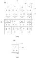
FIG.1 is a structural schematic diagram illustrating a display according to a first embodiment of the present disclosure. -
FIG.2 is a structural schematic diagram illustrating a pixel structure according to the first embodiment shown inFIG. 1 . -
FIG.3 is a structural schematic diagram illustrating a first pixel unit shown inFIG.2 . -
FIG.4 is a structural schematic diagram illustrating a first pixel unit according to a second embodiment of the present disclosure. -
FIG.5 is a structural schematic diagram illustrating a first pixel unit according to a third embodiment of the present disclosure. - As shown in
FIGS. 1-2 , in this embodiment, the display includes apixel structure 10, an integratedcircuit 20 anddiagonal wires 30. The pixel structure includes a plurality of units arranged along a line respectively in both a longitudinal direction and a horizontal direction. Each unit includes afirst pixel unit 100a and a second pixel unit 100b. - Each of the
first pixel unit 100a and the second pixel unit 100b includes a red sub-pixel R, a green sub-pixel G and a blue sub-pixel B. The blue sub-pixel B of thefirst pixel unit 100a is adjacent to the blue sub-pixel B of the second pixel unit 100b. The red sub-pixel R of thefirst pixel unit 100a is axial symmetrical to the red sub-pixel R of the second pixel unit 100b. The green sub-pixel G of thefirst pixel unit 100a is axial symmetrical to the green sub-pixel G of the second pixel unit 100b. In this way, the arrangement of the pixels in the pixel structure is in a form of RGBBGRRGBBGR. - The integrated
circuit 20 has a plurality of ports arranged in a form of sequential red sub-pixel port, green sub-pixel port and blue sub-pixel port repeatedly. - Since the ports on the integrated
circuit 20 are arranged in the form of sequential red sub-pixel port, green sub-pixel port and blue sub-pixel port repeatedly, while the pixels of thepixel structure 10 are arranged in the form of RGBBGRRGBBGR, the output mode and data transmission of the arrangement of the pixels do not match the V-delta structure when the ports are connected to the data lines of the columns of thepixel structure 10 with thediagonal wires 30. Therefore, as shown inFIG. 1 , thediagonal wires 30 include a first crossdiagonal wire 30a and a second crossdiagonal wire 30b. - The first cross
diagonal wire 30a and the second crossdiagonal wire 30b are arranged crosswise. The first crossdiagonal wire 30a is configured to connect a data line of a column where the red sub-pixel of the second pixel unit 100b is positioned, to the red sub-pixel port, and the secondcross diagonal wire 30b is configured to connect a data line of a column where the green sub-pixel of the second pixel unit 100b is positioned, to the green sub-pixel port. In this way, the arrangement of the data transmission of the R and G sub-pixels of the second pixel unit 100b is reversed, so that the output mode and data transmission of the arrangement of the pixels match the V-delta structure. - In this embodiment, as shown in
FIG. 2 , thepixel structure 10 according to the first embodiment includes a plurality of firstpixel unit groups 12 and a plurality of secondpixel unit groups 14. Each of the first and secondpixel unit groups first pixel unit 100a and a second pixel unit 100b. - The
first pixel unit 100a is in a shape of a square. Thefirst pixel unit 100a includes ablue sub-pixel 100, ared sub-pixel 120 and a green sub-pixel. The second pixel unit 100b is mirror-symmetrical to thefirst pixel unit 100a. - Particularly, the first
pixel unit group 12 forms a row, while the secondpixel unit group 14 forms another row. As shown inFIG. 2 , thefirst pixel unit 100a and the second pixel unit 100b are arranged in a mirror-symmetrical form in the horizontal direction. Two adjacentfirst pixel units 100a in the longitudinal direction are arranged in an alternately form, and two adjacent second pixel units 100b in the longitudinal direction are arranged in an alternately form. - As shown in
FIG. 3 , thefirst pixel unit 100a is in a shape of a square, which is divided in two regions including a first region and a second region in a longitudinal direction. Theblue sub-pixel 110 is positioned in the first region, thered sub-pixel 120 and thegreen sub-pixel 130 are positioned in the second region, and there is no overlap between thered sub-pixel 120 and thegreen sub-pixel 130. - In this embodiment, each of the
blue sub-pixel 100, thered sub-pixel 120 and thegreen sub-pixel 130 is in a shape of a rectangle. In particular, theblue sub-pixel 110 is formed in a shape of a rectangle with a side dimension in the row direction longer than another side dimension in the column direction, and each of thered sub-pixel 120 and thegreen sub-pixel 130 are formed in a shape of a rectangle with a side dimension in the column direction longer than another side dimension in the row direction. The side length of thered sub-pixel 120 in the row direction is longer than the side length of thegreen sub-pixel 130 in the row direction, and the side length of thered sub-pixel 120 in the column direction is also longer than the side length of thegreen sub-pixel 130 in the column direction. Thered sub-pixel 120 and thegreen sub-pixel 130 are identical in shape, but different in size. In addition, a sum of the side length of thered sub-pixel 120 in the row direction and the side length of thegreen sub-pixel 130 in the row direction is less than the side length of theblue sub-pixel 110 in the row direction. - In addition, the
blue sub-pixels 110 may be formed by evaporation with a slit-type mask, while thered sub-pixel 120 and thegreen sub-pixel 130 may be formed by evaporation with a slot-type mask. When thered sub-pixels 120 and thegreen sub-pixels 130 are identical in shape, thered sub-pixels 120 and thegreen sub-pixels 130 may be formed by evaporation plating with a common slot-type metal mask. That is to say, a same metal mask may be used for the evaporation for both thered sub-pixel 120 and thegreen sub-pixel 130 to reduce difficulty and cost of the manufacture of the mask. - In addition, if the blue sub-pixel is formed by evaporation with the slit-type mask, and the red sub-pixel and the green sub-pixel are formed by evaporation with a slot-type mask, the masks will have increased opening areas, to reduce difficulty in manufacturing mask. Moreover, it is not required to leave a space between two adjacent sub-pixels during evaporation, so as to improve the PPI of the display, while retaining the opening rate of the mask plate, and also to reduce the weight of the mask and improve the product yield to a certain extent.
- As shown in
FIG. 4 , in this embodiment, thefirst pixel unit 200 is in a shape of a square, which is divided in two regions including a first region and a second region in a longitudinal direction. Theblue sub-pixel 210 is positioned in the first region, thered sub-pixel 220 and thegreen sub-pixel 230 are positioned in the second region, and there is no overlap between thered sub-pixel 220 and thegreen sub-pixel 230. Theblue sub-pixel 210 includes a first blue sub-pixel 21 land a secondblue sub-pixel 212. Each of the first and secondblue sub-pixels blue sub-pixel 211 abuts against a hypotenuse of the secondblue sub-pixel 212. The abutting means that the hypotenuse of the firstblue sub-pixel 211 is parallel to and close to the hypotenuse of the secondblue sub-pixel 212, so as to improve the diagonal effect to a certain extent. - As shown in
FIG. 5 , in this embodiment, thefirst pixel unit 300 is in a shape of a square, which is divided in two regions including a first region and a second region in a longitudinal direction. Theblue sub-pixel 310 is positioned in the first region, thered sub-pixel 320 and thegreen sub-pixel 330 are positioned in the second region, and there is no overlap between thered sub-pixel 320 and thegreen sub-pixel 330. Each of theblue sub-pixel 310, thered sub-pixel 320 and thegreen sub-pixel 330 is in a shape of a circle. In this way, the masks have increased openings. In addition, thered sub-pixel 320 and thegreen sub-pixel 330 may be identical or different in size. - In other embodiments, the
blue sub-pixel 310 may be in a shape of a rectangle or circle, thered sub-pixel 320 may be in a shape of a rectangle, and thegreen sub-pixel 330 may be in a shape of a circle. Alternatively, theblue sub-pixel 310 may be in a shape of a rectangle or circle , thered sub-pixel 320 may be in a shape of a circle, and thegreen sub-pixel 330 may be in a shape of a rectangle. - In the above display, the pixel structure includes a plurality of units, each unit includes a first pixel unit and a second pixel unit, a blue sub-pixel of the first pixel unit is adjacent to a blue sub-pixel of the second pixel unit, a red sub-pixel of the first pixel unit is axial symmetrical to a red sub-pixel of the second pixel unit are arranged, and a green sub-pixel of the first pixel unit is axial symmetrical to a green sub-pixel of the second pixel unit, so that the pixels are arranged in a form of RGBBGRRGBBGR. The integrated circuit has a plurality of ports arranged in a form of a red sub-pixel port, a green sub-pixel port and a blue sub-pixel port in sequence. A first cross diagonal wire and a second cross diagonal wire are provided, the first cross diagonal wire is configured to connect a data line of a column where the red sub-pixel of the second pixel unit is positioned, to the red sub-pixel port, and the second cross diagonal wire is configured to connect a data line of a column where the green sub-pixel of the second pixel unit is positioned, to the green sub-pixel port. In this way, the arrangement of the data transmission of the R and G sub-pixels of the second pixel unit is reversed, so that the output mode and data transmission of the arrangement of the pixels match the V-delta structure.
- Technical features of the above embodiments may be combined arbitrarily. For brief description, not all of the possible combinations of the technical features of the above embodiments are described, but it will be appreciated that these possible combinations belong to the scope of the present disclosure once there is no conflict between the technical features.
- The above are embodiments of the disclosure described in detail, and should not be deemed as limitations to the scope of the present disclosure. It should be noted that variations and improvements will become apparent to those skilled in the art to which the present disclosure pertains without departing from its scope. Therefore, the scope of the present disclosure is defined by the appended claims.
Claims (10)
- A display, comprising:a pixel structure including a plurality of units arranged along a line respectively in both a longitudinal direction and a horizontal direction, wherein each unit includes a first pixel unit and a second pixel unit, each of the first and second pixel units includes a red sub-pixel, a green sub-pixel and a blue sub-pixel, the blue sub-pixel of the first pixel unit is adjacent to the blue sub-pixel of the second pixel unit, the red sub-pixel of the first pixel unit is axial symmetrical to the red sub-pixel of the second pixel unit, and the green sub-pixel of the first pixel unit is axial symmetrical to the green sub-pixel of the second pixel unit;an integrated circuit having a plurality of ports including a plurality of port units arranged in sequence, each port unit including a red sub-pixel port, a green sub-pixel port and a blue sub-pixel port arranged in sequence; anddiagonal wires, configured to connect the plurality of ports to a data line of each column of the pixel structure respectively, the diagonal wires including a first cross diagonal wire and a second cross diagonal wire arranged crosswise, the first cross diagonal wire configured to connect a data line of a column where the red sub-pixel of the second pixel unit is positioned, to the red sub-pixel port, and the second cross diagonal wire configured to connect a data line of a column where the green sub-pixel of the second pixel unit is positioned, to the green sub-pixel port.
- The display of claim 1, wherein the first pixel unit is divided into a first region and a second region in a longitudinal direction, the blue sub-pixel of the first pixel unit is positioned in the first region, the red sub-pixel and the green sub-pixel of the first pixel unit are positioned in the second region, the second pixel unit and the first pixel unit are arranged in a mirror-symmetrical form, the first pixel unit and the second pixel unit adjacent to the first pixel unit in the horizontal direction are arranged in the mirror-symmetrical form, two adjacent first pixel units in the longitudinal direction are arranged in an alternately mirror-symmetrical form, and two adjacent second pixel units in the longitudinal direction are arranged in an alternately mirror-symmetrical form.
- The display of claim 2, wherein the blue sub-pixel of the first pixel unit is formed in a shape of a rectangle with a side dimension in a row direction longer than another side dimension in a column direction, and each of the red sub-pixel and the green sub-pixel of the first pixel unit are respectively formed in a shape of a rectangle with a side dimension in the column direction longer than another side dimension in the row direction.
- The display of claim 2, wherein the red sub-pixel and the green sub-pixel of the first pixel unit are different in size, a side length of the red sub-pixel of the first pixel unit in the row direction is longer than a side length of the green sub-pixel of the first pixel unit in the row direction, and a side length of the red sub-pixel of the first pixel unit in the column direction is longer than a side length of the green sub-pixel of the first pixel unit in the column direction.
- The display of claim 4, wherein a sum of the side length of the red sub-pixel of the first pixel unit in the row direction and the side length of the green sub-pixel of the first pixel in the row direction is less than a side length of the blue sub-pixel of the first pixel unit in the row direction.
- The display of claim 3, wherein the red sub-pixel of the first pixel unit and the green sub-pixel of the first pixel unit are identical in size.
- The display of claim 3, wherein the blue sub-pixel of the first pixel unit includes a first blue sub-pixel and a second blue sub-pixel, each of the first and second blue sub-pixels is formed in a shape of a right triangle, and a hypotenuse of the first blue sub-pixel abuts against a hypotenuse of the second blue sub-pixel.
- The display of claim 2, wherein all of the blue sub-pixel, the red sub-pixel and the green sub-pixel of the first pixel unit are respectively formed in circular.
- The display of claim 2, wherein the blue sub-pixel of the first pixel unit is formed into a rectangular shape, the red sub-pixel of the first pixel unit is formed into a rectangular shape, and the green sub-pixel of the first pixel unit is formed into a circular shape.
- The display of claim 2, wherein the blue sub-pixel of the first pixel unit is formed into a rectangular shape, the red sub-pixel of the first pixel unit is formed into a circular shape, and the green sub-pixel of the first pixel unit is formed into a rectangular shape.
Applications Claiming Priority (2)
| Application Number | Priority Date | Filing Date | Title |
|---|---|---|---|
| CN201620238403.4U CN205487172U (en) | 2016-03-25 | 2016-03-25 | Display |
| PCT/CN2017/076747 WO2017162077A1 (en) | 2016-03-25 | 2017-03-15 | Display |
Publications (3)
| Publication Number | Publication Date |
|---|---|
| EP3382683A1 true EP3382683A1 (en) | 2018-10-03 |
| EP3382683A4 EP3382683A4 (en) | 2019-01-09 |
| EP3382683B1 EP3382683B1 (en) | 2019-10-30 |
Family
ID=56651950
Family Applications (1)
| Application Number | Title | Priority Date | Filing Date |
|---|---|---|---|
| EP17769354.6A Active EP3382683B1 (en) | 2016-03-25 | 2017-03-15 | Display |
Country Status (7)
| Country | Link |
|---|---|
| US (1) | US10680042B2 (en) |
| EP (1) | EP3382683B1 (en) |
| JP (1) | JP6586236B2 (en) |
| KR (1) | KR102115857B1 (en) |
| CN (1) | CN205487172U (en) |
| TW (1) | TWI635607B (en) |
| WO (1) | WO2017162077A1 (en) |
Cited By (2)
| Publication number | Priority date | Publication date | Assignee | Title |
|---|---|---|---|---|
| CN113012630A (en) * | 2020-12-11 | 2021-06-22 | 重庆康佳光电技术研究院有限公司 | Pixel array, manufacturing method of pixel array and display device |
| EP3846215A3 (en) * | 2020-01-02 | 2021-09-08 | Samsung Display Co., Ltd. | Display device |
Families Citing this family (20)
| Publication number | Priority date | Publication date | Assignee | Title |
|---|---|---|---|---|
| CN205487172U (en) * | 2016-03-25 | 2016-08-17 | 昆山工研院新型平板显示技术中心有限公司 | Display |
| KR102390114B1 (en) * | 2017-12-26 | 2022-04-22 | 엘지디스플레이 주식회사 | Organic light emitting display device |
| CN110133885B (en) * | 2018-02-09 | 2024-08-02 | 京东方科技集团股份有限公司 | Pixel arrangement structure, display substrate and display device |
| US11183150B2 (en) | 2019-01-04 | 2021-11-23 | Ati Technologies Ulc | Foveated illumination control at display device |
| CN109755282B (en) * | 2019-01-15 | 2022-04-15 | 武汉天马微电子有限公司 | Display panel and display device |
| KR102866754B1 (en) | 2019-03-04 | 2025-09-30 | 삼성디스플레이 주식회사 | Carrier, apparatus for manufacturing a display apparatus having the same and method for manufacturing a display apparatus |
| US11782190B2 (en) * | 2019-09-06 | 2023-10-10 | Apple Inc. | Optical film arrangements for electronic device displays |
| US12419175B2 (en) | 2019-12-10 | 2025-09-16 | Samsung Display Co., Ltd. | Display device, mask assembly, and apparatus for manufacturing display device |
| US11557635B2 (en) * | 2019-12-10 | 2023-01-17 | Samsung Display Co., Ltd. | Display device, mask assembly, and apparatus for manufacturing the display device |
| CN111834422A (en) * | 2020-06-17 | 2020-10-27 | 深圳市华星光电半导体显示技术有限公司 | Display panel, preparation method thereof and defect repairing method of display panel |
| KR20220000003A (en) * | 2020-06-24 | 2022-01-03 | 삼성디스플레이 주식회사 | Display device |
| CN115884638A (en) * | 2021-05-19 | 2023-03-31 | 上海和辉光电股份有限公司 | Pixel arrangement structure, metal mask plate and organic light-emitting display device |
| CN113707696B (en) * | 2021-08-26 | 2024-11-12 | 京东方科技集团股份有限公司 | Display substrate, mask plate and display device |
| JP7840148B2 (en) * | 2021-12-24 | 2026-04-03 | 武漢天馬微電子有限公司 | Display panels and display devices |
| JPWO2023209494A1 (en) * | 2022-04-29 | 2023-11-02 | ||
| CN115623827A (en) * | 2022-09-29 | 2023-01-17 | 惠科股份有限公司 | Pixel unit and display panel |
| CN115862475B (en) * | 2022-12-15 | 2025-10-17 | 云谷(固安)科技有限公司 | Display panel and display device |
| CN116193921B (en) * | 2023-01-30 | 2023-09-12 | 上海和辉光电股份有限公司 | Pixel arrangement structure, metal mask plate, display panel and display device |
| US12401777B2 (en) | 2023-04-12 | 2025-08-26 | Apple Inc. | Pixel arrangements for displays with lenticular lenses |
| CN120166885B (en) * | 2025-03-06 | 2026-04-14 | 武汉天马微电子有限公司 | Pixel arrangement structure, mask plate assembly and display panel |
Family Cites Families (17)
| Publication number | Priority date | Publication date | Assignee | Title |
|---|---|---|---|---|
| TWI274221B (en) | 2005-09-29 | 2007-02-21 | Au Optronics Corp | Active device matrix substrate |
| KR101358334B1 (en) | 2007-07-24 | 2014-02-06 | 삼성디스플레이 주식회사 | Liquid crystal display and method of driving the same |
| JP4409589B2 (en) | 2007-07-31 | 2010-02-03 | 株式会社 日立ディスプレイズ | Liquid crystal display |
| KR101499234B1 (en) | 2008-06-27 | 2015-03-05 | 삼성디스플레이 주식회사 | Organic light emitting device, method of manufacturing the same and shadow mask therefor |
| TW201102731A (en) | 2009-07-15 | 2011-01-16 | Chi Mei Optoelectronics Corp | Active device array substrate and liquid crystal display apparatus |
| JP2011096378A (en) | 2009-10-27 | 2011-05-12 | Canon Inc | Organic el display device |
| EP2579092A1 (en) | 2010-06-02 | 2013-04-10 | Sharp Kabushiki Kaisha | Liquid crystal display device and display defect correction method |
| JP2013058323A (en) | 2011-09-07 | 2013-03-28 | Sony Corp | Light-emitting panel, display device, and electronic apparatus |
| KR102127762B1 (en) * | 2013-10-02 | 2020-06-30 | 삼성디스플레이 주식회사 | Flat panel display device |
| CN104752469B (en) | 2013-12-31 | 2018-08-03 | 昆山国显光电有限公司 | A pixel structure and an organic light-emitting display using the pixel structure |
| CN104037197B (en) * | 2013-12-31 | 2017-06-16 | 昆山国显光电有限公司 | A kind of dot structure and the OLED using the dot structure |
| TWI537928B (en) | 2014-01-27 | 2016-06-11 | 友達光電股份有限公司 | Display panel and driving method thereof |
| CN204257652U (en) | 2014-12-19 | 2015-04-08 | 昆山国显光电有限公司 | The dot structure of display and display |
| US20170032749A1 (en) * | 2015-07-28 | 2017-02-02 | Shenzhen China Star Optoelectronics Technology Co. Ltd. | Liquid crystal display device |
| CN105093737A (en) * | 2015-07-28 | 2015-11-25 | 深圳市华星光电技术有限公司 | Liquid crystal display |
| KR102526751B1 (en) * | 2016-01-25 | 2023-04-27 | 삼성전자주식회사 | Directional backlight unit, three dimensional image display apparatus, and method of displaying three dimensional image display |
| CN205487172U (en) | 2016-03-25 | 2016-08-17 | 昆山工研院新型平板显示技术中心有限公司 | Display |
-
2016
- 2016-03-25 CN CN201620238403.4U patent/CN205487172U/en not_active Expired - Lifetime
-
2017
- 2017-03-15 WO PCT/CN2017/076747 patent/WO2017162077A1/en not_active Ceased
- 2017-03-15 KR KR1020187017605A patent/KR102115857B1/en active Active
- 2017-03-15 JP JP2018533146A patent/JP6586236B2/en active Active
- 2017-03-15 EP EP17769354.6A patent/EP3382683B1/en active Active
- 2017-03-15 US US15/781,631 patent/US10680042B2/en active Active
- 2017-03-23 TW TW106109827A patent/TWI635607B/en active
Cited By (6)
| Publication number | Priority date | Publication date | Assignee | Title |
|---|---|---|---|---|
| EP3846215A3 (en) * | 2020-01-02 | 2021-09-08 | Samsung Display Co., Ltd. | Display device |
| US11672153B2 (en) | 2020-01-02 | 2023-06-06 | Samsung Display Co., Ltd. | Display device including a connected and/or shared intermediate layer |
| US11980078B2 (en) | 2020-01-02 | 2024-05-07 | Samsung Display Co., Ltd. | Display device |
| US12329011B2 (en) | 2020-01-02 | 2025-06-10 | Samsung Display Co., Ltd. | Display device including auxiliary sub-pixels having connected intermediate layers |
| CN113012630A (en) * | 2020-12-11 | 2021-06-22 | 重庆康佳光电技术研究院有限公司 | Pixel array, manufacturing method of pixel array and display device |
| CN113012630B (en) * | 2020-12-11 | 2022-05-31 | 重庆康佳光电技术研究院有限公司 | Pixel array, manufacturing method of pixel array and display device |
Also Published As
| Publication number | Publication date |
|---|---|
| US10680042B2 (en) | 2020-06-09 |
| JP6586236B2 (en) | 2019-10-02 |
| TWI635607B (en) | 2018-09-11 |
| WO2017162077A1 (en) | 2017-09-28 |
| TW201803106A (en) | 2018-01-16 |
| KR102115857B1 (en) | 2020-05-27 |
| US20190378882A1 (en) | 2019-12-12 |
| KR20180084975A (en) | 2018-07-25 |
| CN205487172U (en) | 2016-08-17 |
| JP2019503049A (en) | 2019-01-31 |
| EP3382683B1 (en) | 2019-10-30 |
| EP3382683A4 (en) | 2019-01-09 |
Similar Documents
| Publication | Publication Date | Title |
|---|---|---|
| EP3382683A1 (en) | Display | |
| CN205231065U (en) | Dot structure and display | |
| CN103345887B (en) | Pixel array and display with same | |
| US10210787B2 (en) | Display panel and display device | |
| JP2022046648A5 (en) | Pixel array structure and display device | |
| US8354789B2 (en) | Pixel arrangement of an organic light emitting display device | |
| CN103325315B (en) | Pixel array and display with same | |
| US9655201B2 (en) | Pixel arrangement structure for organic light-emitting diode display panel | |
| US9734795B2 (en) | Pixel array and driving method thereof, display panel and display device | |
| CN106991957B (en) | A pixel structure, a display substrate, a display device and a display method | |
| US10224378B2 (en) | Organic light emitting device (OLED) pixel arrangement structure | |
| CN205231067U (en) | Pixel , dot structure and display | |
| MX2021016051A (en) | SERIES OF PIXELS AND DISPLAY DEVICE. | |
| CN109300958A (en) | A pixel structure, a display panel and a display device | |
| CN110720146A (en) | Pixel array, display panel and electronic device | |
| CN107610644A (en) | Dot structure, display panel, the driving method of display device and display panel | |
| CN104778919A (en) | OLED panel, driving method and FMM for evaporation | |
| CN105097865A (en) | Pixel arrangement structure for AMOLED (Active Matrix/Organic Light Emitting Diode) display | |
| CN105529353A (en) | Display and pixel structure therefor | |
| CN109148547B (en) | Pixel arrangement structure and display panel | |
| KR20150106622A (en) | Organic light emitting display apparatus | |
| CN104460090B (en) | A kind of display device | |
| US9552757B2 (en) | Image device with improved chrominance quality | |
| CN105093631B (en) | Dot structure, array substrate, display device and sub-pixel rendering intent | |
| CN112074895A (en) | Pixel arrangement structure, display substrate and display device |
Legal Events
| Date | Code | Title | Description |
|---|---|---|---|
| STAA | Information on the status of an ep patent application or granted ep patent |
Free format text: STATUS: THE INTERNATIONAL PUBLICATION HAS BEEN MADE |
|
| PUAI | Public reference made under article 153(3) epc to a published international application that has entered the european phase |
Free format text: ORIGINAL CODE: 0009012 |
|
| STAA | Information on the status of an ep patent application or granted ep patent |
Free format text: STATUS: REQUEST FOR EXAMINATION WAS MADE |
|
| 17P | Request for examination filed |
Effective date: 20180605 |
|
| AK | Designated contracting states |
Kind code of ref document: A1 Designated state(s): AL AT BE BG CH CY CZ DE DK EE ES FI FR GB GR HR HU IE IS IT LI LT LU LV MC MK MT NL NO PL PT RO RS SE SI SK SM TR |
|
| AX | Request for extension of the european patent |
Extension state: BA ME |
|
| A4 | Supplementary search report drawn up and despatched |
Effective date: 20181207 |
|
| RIC1 | Information provided on ipc code assigned before grant |
Ipc: H01L 27/32 20060101AFI20181203BHEP |
|
| REG | Reference to a national code |
Ref country code: DE Ref legal event code: R079 Ref document number: 602017008286 Country of ref document: DE Free format text: PREVIOUS MAIN CLASS: G09F0009330000 Ipc: H01L0027320000 |
|
| DAV | Request for validation of the european patent (deleted) | ||
| DAX | Request for extension of the european patent (deleted) | ||
| GRAP | Despatch of communication of intention to grant a patent |
Free format text: ORIGINAL CODE: EPIDOSNIGR1 |
|
| STAA | Information on the status of an ep patent application or granted ep patent |
Free format text: STATUS: GRANT OF PATENT IS INTENDED |
|
| RIC1 | Information provided on ipc code assigned before grant |
Ipc: H01L 27/32 20060101AFI20190620BHEP Ipc: G09G 3/3275 20160101ALI20190620BHEP |
|
| INTG | Intention to grant announced |
Effective date: 20190719 |
|
| GRAS | Grant fee paid |
Free format text: ORIGINAL CODE: EPIDOSNIGR3 |
|
| GRAA | (expected) grant |
Free format text: ORIGINAL CODE: 0009210 |
|
| STAA | Information on the status of an ep patent application or granted ep patent |
Free format text: STATUS: THE PATENT HAS BEEN GRANTED |
|
| AK | Designated contracting states |
Kind code of ref document: B1 Designated state(s): AL AT BE BG CH CY CZ DE DK EE ES FI FR GB GR HR HU IE IS IT LI LT LU LV MC MK MT NL NO PL PT RO RS SE SI SK SM TR |
|
| REG | Reference to a national code |
Ref country code: GB Ref legal event code: FG4D |
|
| REG | Reference to a national code |
Ref country code: CH Ref legal event code: EP |
|
| REG | Reference to a national code |
Ref country code: AT Ref legal event code: REF Ref document number: 1197079 Country of ref document: AT Kind code of ref document: T Effective date: 20191115 |
|
| REG | Reference to a national code |
Ref country code: DE Ref legal event code: R096 Ref document number: 602017008286 Country of ref document: DE |
|
| REG | Reference to a national code |
Ref country code: IE Ref legal event code: FG4D |
|
| REG | Reference to a national code |
Ref country code: LT Ref legal event code: MG4D |
|
| PG25 | Lapsed in a contracting state [announced via postgrant information from national office to epo] |
Ref country code: BG Free format text: LAPSE BECAUSE OF FAILURE TO SUBMIT A TRANSLATION OF THE DESCRIPTION OR TO PAY THE FEE WITHIN THE PRESCRIBED TIME-LIMIT Effective date: 20200130 Ref country code: FI Free format text: LAPSE BECAUSE OF FAILURE TO SUBMIT A TRANSLATION OF THE DESCRIPTION OR TO PAY THE FEE WITHIN THE PRESCRIBED TIME-LIMIT Effective date: 20191030 Ref country code: PT Free format text: LAPSE BECAUSE OF FAILURE TO SUBMIT A TRANSLATION OF THE DESCRIPTION OR TO PAY THE FEE WITHIN THE PRESCRIBED TIME-LIMIT Effective date: 20200302 Ref country code: PL Free format text: LAPSE BECAUSE OF FAILURE TO SUBMIT A TRANSLATION OF THE DESCRIPTION OR TO PAY THE FEE WITHIN THE PRESCRIBED TIME-LIMIT Effective date: 20191030 Ref country code: NL Free format text: LAPSE BECAUSE OF FAILURE TO SUBMIT A TRANSLATION OF THE DESCRIPTION OR TO PAY THE FEE WITHIN THE PRESCRIBED TIME-LIMIT Effective date: 20191030 Ref country code: SE Free format text: LAPSE BECAUSE OF FAILURE TO SUBMIT A TRANSLATION OF THE DESCRIPTION OR TO PAY THE FEE WITHIN THE PRESCRIBED TIME-LIMIT Effective date: 20191030 Ref country code: LV Free format text: LAPSE BECAUSE OF FAILURE TO SUBMIT A TRANSLATION OF THE DESCRIPTION OR TO PAY THE FEE WITHIN THE PRESCRIBED TIME-LIMIT Effective date: 20191030 Ref country code: NO Free format text: LAPSE BECAUSE OF FAILURE TO SUBMIT A TRANSLATION OF THE DESCRIPTION OR TO PAY THE FEE WITHIN THE PRESCRIBED TIME-LIMIT Effective date: 20200130 Ref country code: LT Free format text: LAPSE BECAUSE OF FAILURE TO SUBMIT A TRANSLATION OF THE DESCRIPTION OR TO PAY THE FEE WITHIN THE PRESCRIBED TIME-LIMIT Effective date: 20191030 Ref country code: GR Free format text: LAPSE BECAUSE OF FAILURE TO SUBMIT A TRANSLATION OF THE DESCRIPTION OR TO PAY THE FEE WITHIN THE PRESCRIBED TIME-LIMIT Effective date: 20200131 |
|
| REG | Reference to a national code |
Ref country code: NL Ref legal event code: MP Effective date: 20191030 |
|
| PG25 | Lapsed in a contracting state [announced via postgrant information from national office to epo] |
Ref country code: HR Free format text: LAPSE BECAUSE OF FAILURE TO SUBMIT A TRANSLATION OF THE DESCRIPTION OR TO PAY THE FEE WITHIN THE PRESCRIBED TIME-LIMIT Effective date: 20191030 Ref country code: IS Free format text: LAPSE BECAUSE OF FAILURE TO SUBMIT A TRANSLATION OF THE DESCRIPTION OR TO PAY THE FEE WITHIN THE PRESCRIBED TIME-LIMIT Effective date: 20200229 Ref country code: RS Free format text: LAPSE BECAUSE OF FAILURE TO SUBMIT A TRANSLATION OF THE DESCRIPTION OR TO PAY THE FEE WITHIN THE PRESCRIBED TIME-LIMIT Effective date: 20191030 |
|
| PG25 | Lapsed in a contracting state [announced via postgrant information from national office to epo] |
Ref country code: AL Free format text: LAPSE BECAUSE OF FAILURE TO SUBMIT A TRANSLATION OF THE DESCRIPTION OR TO PAY THE FEE WITHIN THE PRESCRIBED TIME-LIMIT Effective date: 20191030 |
|
| PG25 | Lapsed in a contracting state [announced via postgrant information from national office to epo] |
Ref country code: DK Free format text: LAPSE BECAUSE OF FAILURE TO SUBMIT A TRANSLATION OF THE DESCRIPTION OR TO PAY THE FEE WITHIN THE PRESCRIBED TIME-LIMIT Effective date: 20191030 Ref country code: EE Free format text: LAPSE BECAUSE OF FAILURE TO SUBMIT A TRANSLATION OF THE DESCRIPTION OR TO PAY THE FEE WITHIN THE PRESCRIBED TIME-LIMIT Effective date: 20191030 Ref country code: ES Free format text: LAPSE BECAUSE OF FAILURE TO SUBMIT A TRANSLATION OF THE DESCRIPTION OR TO PAY THE FEE WITHIN THE PRESCRIBED TIME-LIMIT Effective date: 20191030 Ref country code: RO Free format text: LAPSE BECAUSE OF FAILURE TO SUBMIT A TRANSLATION OF THE DESCRIPTION OR TO PAY THE FEE WITHIN THE PRESCRIBED TIME-LIMIT Effective date: 20191030 Ref country code: CZ Free format text: LAPSE BECAUSE OF FAILURE TO SUBMIT A TRANSLATION OF THE DESCRIPTION OR TO PAY THE FEE WITHIN THE PRESCRIBED TIME-LIMIT Effective date: 20191030 |
|
| REG | Reference to a national code |
Ref country code: DE Ref legal event code: R097 Ref document number: 602017008286 Country of ref document: DE |
|
| REG | Reference to a national code |
Ref country code: AT Ref legal event code: MK05 Ref document number: 1197079 Country of ref document: AT Kind code of ref document: T Effective date: 20191030 |
|
| PG25 | Lapsed in a contracting state [announced via postgrant information from national office to epo] |
Ref country code: SM Free format text: LAPSE BECAUSE OF FAILURE TO SUBMIT A TRANSLATION OF THE DESCRIPTION OR TO PAY THE FEE WITHIN THE PRESCRIBED TIME-LIMIT Effective date: 20191030 Ref country code: IT Free format text: LAPSE BECAUSE OF FAILURE TO SUBMIT A TRANSLATION OF THE DESCRIPTION OR TO PAY THE FEE WITHIN THE PRESCRIBED TIME-LIMIT Effective date: 20191030 Ref country code: SK Free format text: LAPSE BECAUSE OF FAILURE TO SUBMIT A TRANSLATION OF THE DESCRIPTION OR TO PAY THE FEE WITHIN THE PRESCRIBED TIME-LIMIT Effective date: 20191030 |
|
| PLBE | No opposition filed within time limit |
Free format text: ORIGINAL CODE: 0009261 |
|
| STAA | Information on the status of an ep patent application or granted ep patent |
Free format text: STATUS: NO OPPOSITION FILED WITHIN TIME LIMIT |
|
| 26N | No opposition filed |
Effective date: 20200731 |
|
| PG25 | Lapsed in a contracting state [announced via postgrant information from national office to epo] |
Ref country code: MC Free format text: LAPSE BECAUSE OF FAILURE TO SUBMIT A TRANSLATION OF THE DESCRIPTION OR TO PAY THE FEE WITHIN THE PRESCRIBED TIME-LIMIT Effective date: 20191030 |
|
| REG | Reference to a national code |
Ref country code: CH Ref legal event code: PL |
|
| PG25 | Lapsed in a contracting state [announced via postgrant information from national office to epo] |
Ref country code: SI Free format text: LAPSE BECAUSE OF FAILURE TO SUBMIT A TRANSLATION OF THE DESCRIPTION OR TO PAY THE FEE WITHIN THE PRESCRIBED TIME-LIMIT Effective date: 20191030 Ref country code: AT Free format text: LAPSE BECAUSE OF FAILURE TO SUBMIT A TRANSLATION OF THE DESCRIPTION OR TO PAY THE FEE WITHIN THE PRESCRIBED TIME-LIMIT Effective date: 20191030 |
|
| REG | Reference to a national code |
Ref country code: BE Ref legal event code: MM Effective date: 20200331 |
|
| PG25 | Lapsed in a contracting state [announced via postgrant information from national office to epo] |
Ref country code: LU Free format text: LAPSE BECAUSE OF NON-PAYMENT OF DUE FEES Effective date: 20200315 |
|
| PG25 | Lapsed in a contracting state [announced via postgrant information from national office to epo] |
Ref country code: IE Free format text: LAPSE BECAUSE OF NON-PAYMENT OF DUE FEES Effective date: 20200315 Ref country code: CH Free format text: LAPSE BECAUSE OF NON-PAYMENT OF DUE FEES Effective date: 20200331 Ref country code: LI Free format text: LAPSE BECAUSE OF NON-PAYMENT OF DUE FEES Effective date: 20200331 |
|
| PG25 | Lapsed in a contracting state [announced via postgrant information from national office to epo] |
Ref country code: BE Free format text: LAPSE BECAUSE OF NON-PAYMENT OF DUE FEES Effective date: 20200331 |
|
| PG25 | Lapsed in a contracting state [announced via postgrant information from national office to epo] |
Ref country code: TR Free format text: LAPSE BECAUSE OF FAILURE TO SUBMIT A TRANSLATION OF THE DESCRIPTION OR TO PAY THE FEE WITHIN THE PRESCRIBED TIME-LIMIT Effective date: 20191030 Ref country code: MT Free format text: LAPSE BECAUSE OF FAILURE TO SUBMIT A TRANSLATION OF THE DESCRIPTION OR TO PAY THE FEE WITHIN THE PRESCRIBED TIME-LIMIT Effective date: 20191030 Ref country code: CY Free format text: LAPSE BECAUSE OF FAILURE TO SUBMIT A TRANSLATION OF THE DESCRIPTION OR TO PAY THE FEE WITHIN THE PRESCRIBED TIME-LIMIT Effective date: 20191030 |
|
| PG25 | Lapsed in a contracting state [announced via postgrant information from national office to epo] |
Ref country code: MK Free format text: LAPSE BECAUSE OF FAILURE TO SUBMIT A TRANSLATION OF THE DESCRIPTION OR TO PAY THE FEE WITHIN THE PRESCRIBED TIME-LIMIT Effective date: 20191030 |
|
| REG | Reference to a national code |
Ref country code: DE Ref legal event code: R079 Ref document number: 602017008286 Country of ref document: DE Free format text: PREVIOUS MAIN CLASS: H01L0027320000 Ipc: H10K0059000000 |
|
| P01 | Opt-out of the competence of the unified patent court (upc) registered |
Effective date: 20230526 |
|
| PGFP | Annual fee paid to national office [announced via postgrant information from national office to epo] |
Ref country code: GB Payment date: 20260323 Year of fee payment: 10 |
|
| PGFP | Annual fee paid to national office [announced via postgrant information from national office to epo] |
Ref country code: DE Payment date: 20260313 Year of fee payment: 10 |
|
| PGFP | Annual fee paid to national office [announced via postgrant information from national office to epo] |
Ref country code: FR Payment date: 20260330 Year of fee payment: 10 |