EP3380644B1 - Verfahren zur erzeugung von dünnen anorganischen filmen - Google Patents
Verfahren zur erzeugung von dünnen anorganischen filmen Download PDFInfo
- Publication number
- EP3380644B1 EP3380644B1 EP16798703.1A EP16798703A EP3380644B1 EP 3380644 B1 EP3380644 B1 EP 3380644B1 EP 16798703 A EP16798703 A EP 16798703A EP 3380644 B1 EP3380644 B1 EP 3380644B1
- Authority
- EP
- European Patent Office
- Prior art keywords
- compound
- general formula
- process according
- methyl
- ligand
- Prior art date
- Legal status (The legal status is an assumption and is not a legal conclusion. Google has not performed a legal analysis and makes no representation as to the accuracy of the status listed.)
- Active
Links
- 238000000034 method Methods 0.000 title claims description 56
- 230000008569 process Effects 0.000 title claims description 48
- 150000001875 compounds Chemical class 0.000 claims description 89
- 239000000758 substrate Substances 0.000 claims description 49
- 239000003446 ligand Substances 0.000 claims description 47
- 239000007787 solid Substances 0.000 claims description 36
- 125000000217 alkyl group Chemical group 0.000 claims description 20
- 239000000443 aerosol Substances 0.000 claims description 19
- 125000003118 aryl group Chemical group 0.000 claims description 12
- 238000000151 deposition Methods 0.000 claims description 12
- 125000002496 methyl group Chemical group [H]C([H])([H])* 0.000 claims description 12
- 229910052759 nickel Inorganic materials 0.000 claims description 11
- 125000004665 trialkylsilyl group Chemical group 0.000 claims description 10
- 239000003638 chemical reducing agent Substances 0.000 claims description 7
- 230000007935 neutral effect Effects 0.000 claims description 7
- 125000001495 ethyl group Chemical group [H]C([H])([H])C([H])([H])* 0.000 claims description 6
- 229910052748 manganese Inorganic materials 0.000 claims description 6
- OAICVXFJPJFONN-UHFFFAOYSA-N Phosphorus Chemical group [P] OAICVXFJPJFONN-UHFFFAOYSA-N 0.000 claims description 3
- 230000015572 biosynthetic process Effects 0.000 claims description 3
- MWUXSHHQAYIFBG-UHFFFAOYSA-N Nitric oxide Chemical compound O=[N] MWUXSHHQAYIFBG-UHFFFAOYSA-N 0.000 description 88
- UGFAIRIUMAVXCW-UHFFFAOYSA-N Carbon monoxide Chemical compound [O+]#[C-] UGFAIRIUMAVXCW-UHFFFAOYSA-N 0.000 description 69
- 229910002091 carbon monoxide Inorganic materials 0.000 description 69
- 229940105305 carbon monoxide Drugs 0.000 description 69
- -1 n-octyl Chemical group 0.000 description 61
- 239000010408 film Substances 0.000 description 42
- YWWDBCBWQNCYNR-UHFFFAOYSA-N trimethylphosphine Chemical compound CP(C)C YWWDBCBWQNCYNR-UHFFFAOYSA-N 0.000 description 41
- PXHVJJICTQNCMI-UHFFFAOYSA-N Nickel Chemical compound [Ni] PXHVJJICTQNCMI-UHFFFAOYSA-N 0.000 description 17
- 229910052751 metal Inorganic materials 0.000 description 15
- 239000002184 metal Substances 0.000 description 15
- 238000000354 decomposition reaction Methods 0.000 description 14
- 239000010410 layer Substances 0.000 description 14
- 229910052757 nitrogen Inorganic materials 0.000 description 14
- QGZKDVFQNNGYKY-UHFFFAOYSA-N Ammonia Chemical compound N QGZKDVFQNNGYKY-UHFFFAOYSA-N 0.000 description 13
- WYURNTSHIVDZCO-UHFFFAOYSA-N Tetrahydrofuran Chemical compound C1CCOC1 WYURNTSHIVDZCO-UHFFFAOYSA-N 0.000 description 13
- 239000011572 manganese Substances 0.000 description 13
- YXFVVABEGXRONW-UHFFFAOYSA-N Toluene Chemical compound CC1=CC=CC=C1 YXFVVABEGXRONW-UHFFFAOYSA-N 0.000 description 12
- UHOVQNZJYSORNB-MZWXYZOWSA-N benzene-d6 Chemical compound [2H]C1=C([2H])C([2H])=C([2H])C([2H])=C1[2H] UHOVQNZJYSORNB-MZWXYZOWSA-N 0.000 description 12
- 239000002904 solvent Substances 0.000 description 11
- IJGRMHOSHXDMSA-UHFFFAOYSA-N Atomic nitrogen Chemical compound N#N IJGRMHOSHXDMSA-UHFFFAOYSA-N 0.000 description 10
- OFBQJSOFQDEBGM-UHFFFAOYSA-N Pentane Chemical compound CCCCC OFBQJSOFQDEBGM-UHFFFAOYSA-N 0.000 description 10
- VLKZOEOYAKHREP-UHFFFAOYSA-N n-Hexane Chemical compound CCCCCC VLKZOEOYAKHREP-UHFFFAOYSA-N 0.000 description 9
- XNMQEEKYCVKGBD-UHFFFAOYSA-N 2-butyne Chemical compound CC#CC XNMQEEKYCVKGBD-UHFFFAOYSA-N 0.000 description 8
- 230000008021 deposition Effects 0.000 description 8
- 239000001257 hydrogen Substances 0.000 description 8
- 229910052739 hydrogen Inorganic materials 0.000 description 8
- 239000000243 solution Substances 0.000 description 8
- BUHVIAUBTBOHAG-FOYDDCNASA-N (2r,3r,4s,5r)-2-[6-[[2-(3,5-dimethoxyphenyl)-2-(2-methylphenyl)ethyl]amino]purin-9-yl]-5-(hydroxymethyl)oxolane-3,4-diol Chemical compound COC1=CC(OC)=CC(C(CNC=2C=3N=CN(C=3N=CN=2)[C@H]2[C@@H]([C@H](O)[C@@H](CO)O2)O)C=2C(=CC=CC=2)C)=C1 BUHVIAUBTBOHAG-FOYDDCNASA-N 0.000 description 7
- 229910021529 ammonia Inorganic materials 0.000 description 7
- 238000000231 atomic layer deposition Methods 0.000 description 7
- 239000002245 particle Substances 0.000 description 7
- 239000000725 suspension Substances 0.000 description 7
- UHOVQNZJYSORNB-UHFFFAOYSA-N Benzene Chemical compound C1=CC=CC=C1 UHOVQNZJYSORNB-UHFFFAOYSA-N 0.000 description 6
- OAKJQQAXSVQMHS-UHFFFAOYSA-N Hydrazine Chemical compound NN OAKJQQAXSVQMHS-UHFFFAOYSA-N 0.000 description 6
- VYPSYNLAJGMNEJ-UHFFFAOYSA-N Silicium dioxide Chemical compound O=[Si]=O VYPSYNLAJGMNEJ-UHFFFAOYSA-N 0.000 description 6
- 239000007788 liquid Substances 0.000 description 6
- 239000001301 oxygen Substances 0.000 description 6
- 229910052760 oxygen Inorganic materials 0.000 description 6
- YLQBMQCUIZJEEH-UHFFFAOYSA-N tetrahydrofuran Natural products C=1C=COC=1 YLQBMQCUIZJEEH-UHFFFAOYSA-N 0.000 description 6
- XLYOFNOQVPJJNP-UHFFFAOYSA-N water Chemical class O XLYOFNOQVPJJNP-UHFFFAOYSA-N 0.000 description 6
- XFXPMWWXUTWYJX-UHFFFAOYSA-N Cyanide Chemical compound N#[C-] XFXPMWWXUTWYJX-UHFFFAOYSA-N 0.000 description 5
- UFHFLCQGNIYNRP-UHFFFAOYSA-N Hydrogen Chemical compound [H][H] UFHFLCQGNIYNRP-UHFFFAOYSA-N 0.000 description 5
- QVGXLLKOCUKJST-UHFFFAOYSA-N atomic oxygen Chemical compound [O] QVGXLLKOCUKJST-UHFFFAOYSA-N 0.000 description 5
- 229910052799 carbon Inorganic materials 0.000 description 5
- 239000013078 crystal Substances 0.000 description 5
- 238000001704 evaporation Methods 0.000 description 5
- 230000008020 evaporation Effects 0.000 description 5
- 125000004433 nitrogen atom Chemical group N* 0.000 description 5
- 239000003921 oil Substances 0.000 description 5
- 239000002243 precursor Substances 0.000 description 5
- 235000012239 silicon dioxide Nutrition 0.000 description 5
- RHUYHJGZWVXEHW-UHFFFAOYSA-N 1,1-Dimethyhydrazine Chemical compound CN(C)N RHUYHJGZWVXEHW-UHFFFAOYSA-N 0.000 description 4
- 238000005160 1H NMR spectroscopy Methods 0.000 description 4
- CPELXLSAUQHCOX-UHFFFAOYSA-M Bromide Chemical compound [Br-] CPELXLSAUQHCOX-UHFFFAOYSA-M 0.000 description 4
- GQPLMRYTRLFLPF-UHFFFAOYSA-N Nitrous Oxide Chemical compound [O-][N+]#N GQPLMRYTRLFLPF-UHFFFAOYSA-N 0.000 description 4
- JUJWROOIHBZHMG-UHFFFAOYSA-N Pyridine Chemical compound C1=CC=NC=C1 JUJWROOIHBZHMG-UHFFFAOYSA-N 0.000 description 4
- XUIMIQQOPSSXEZ-UHFFFAOYSA-N Silicon Chemical group [Si] XUIMIQQOPSSXEZ-UHFFFAOYSA-N 0.000 description 4
- PPBRXRYQALVLMV-UHFFFAOYSA-N Styrene Chemical compound C=CC1=CC=CC=C1 PPBRXRYQALVLMV-UHFFFAOYSA-N 0.000 description 4
- 238000004833 X-ray photoelectron spectroscopy Methods 0.000 description 4
- 229910000071 diazene Inorganic materials 0.000 description 4
- 238000010438 heat treatment Methods 0.000 description 4
- FFUAGWLWBBFQJT-UHFFFAOYSA-N hexamethyldisilazane Chemical compound C[Si](C)(C)N[Si](C)(C)C FFUAGWLWBBFQJT-UHFFFAOYSA-N 0.000 description 4
- 229910044991 metal oxide Inorganic materials 0.000 description 4
- 150000004706 metal oxides Chemical class 0.000 description 4
- 150000002739 metals Chemical class 0.000 description 4
- 150000004767 nitrides Chemical class 0.000 description 4
- 239000012299 nitrogen atmosphere Substances 0.000 description 4
- 239000010453 quartz Substances 0.000 description 4
- 229910052710 silicon Inorganic materials 0.000 description 4
- 239000010703 silicon Substances 0.000 description 4
- 238000003756 stirring Methods 0.000 description 4
- 238000002411 thermogravimetry Methods 0.000 description 4
- 125000000026 trimethylsilyl group Chemical group [H]C([H])([H])[Si]([*])(C([H])([H])[H])C([H])([H])[H] 0.000 description 4
- 238000001644 13C nuclear magnetic resonance spectroscopy Methods 0.000 description 3
- RWRDLPDLKQPQOW-UHFFFAOYSA-N Pyrrolidine Chemical compound C1CCNC1 RWRDLPDLKQPQOW-UHFFFAOYSA-N 0.000 description 3
- 125000001931 aliphatic group Chemical group 0.000 description 3
- 150000001412 amines Chemical class 0.000 description 3
- 125000004429 atom Chemical group 0.000 description 3
- 238000005229 chemical vapour deposition Methods 0.000 description 3
- 229910017052 cobalt Inorganic materials 0.000 description 3
- 239000010941 cobalt Substances 0.000 description 3
- GUTLYIVDDKVIGB-UHFFFAOYSA-N cobalt atom Chemical compound [Co] GUTLYIVDDKVIGB-UHFFFAOYSA-N 0.000 description 3
- 230000007547 defect Effects 0.000 description 3
- 238000005137 deposition process Methods 0.000 description 3
- 229910052736 halogen Inorganic materials 0.000 description 3
- 150000002367 halogens Chemical class 0.000 description 3
- 239000000463 material Substances 0.000 description 3
- HZVOZRGWRWCICA-UHFFFAOYSA-N methanediyl Chemical class [CH2] HZVOZRGWRWCICA-UHFFFAOYSA-N 0.000 description 3
- 239000004065 semiconductor Substances 0.000 description 3
- 239000002356 single layer Substances 0.000 description 3
- 239000000126 substance Substances 0.000 description 3
- 229930195735 unsaturated hydrocarbon Natural products 0.000 description 3
- RRKODOZNUZCUBN-CCAGOZQPSA-N (1z,3z)-cycloocta-1,3-diene Chemical compound C1CC\C=C/C=C\C1 RRKODOZNUZCUBN-CCAGOZQPSA-N 0.000 description 2
- 125000004169 (C1-C6) alkyl group Chemical group 0.000 description 2
- DHKHKXVYLBGOIT-UHFFFAOYSA-N 1,1-Diethoxyethane Chemical compound CCOC(C)OCC DHKHKXVYLBGOIT-UHFFFAOYSA-N 0.000 description 2
- 125000003903 2-propenyl group Chemical group [H]C([*])([H])C([H])=C([H])[H] 0.000 description 2
- DLFVBJFMPXGRIB-UHFFFAOYSA-N Acetamide Chemical compound CC(N)=O DLFVBJFMPXGRIB-UHFFFAOYSA-N 0.000 description 2
- HSFWRNGVRCDJHI-UHFFFAOYSA-N Acetylene Chemical compound C#C HSFWRNGVRCDJHI-UHFFFAOYSA-N 0.000 description 2
- XKRFYHLGVUSROY-UHFFFAOYSA-N Argon Chemical compound [Ar] XKRFYHLGVUSROY-UHFFFAOYSA-N 0.000 description 2
- OKTJSMMVPCPJKN-UHFFFAOYSA-N Carbon Chemical compound [C] OKTJSMMVPCPJKN-UHFFFAOYSA-N 0.000 description 2
- 239000004215 Carbon black (E152) Substances 0.000 description 2
- VEXZGXHMUGYJMC-UHFFFAOYSA-M Chloride anion Chemical compound [Cl-] VEXZGXHMUGYJMC-UHFFFAOYSA-M 0.000 description 2
- RYGMFSIKBFXOCR-UHFFFAOYSA-N Copper Chemical compound [Cu] RYGMFSIKBFXOCR-UHFFFAOYSA-N 0.000 description 2
- ROSDSFDQCJNGOL-UHFFFAOYSA-N Dimethylamine Chemical compound CNC ROSDSFDQCJNGOL-UHFFFAOYSA-N 0.000 description 2
- KRHYYFGTRYWZRS-UHFFFAOYSA-M Fluoride anion Chemical compound [F-] KRHYYFGTRYWZRS-UHFFFAOYSA-M 0.000 description 2
- ZHNUHDYFZUAESO-UHFFFAOYSA-N Formamide Chemical compound NC=O ZHNUHDYFZUAESO-UHFFFAOYSA-N 0.000 description 2
- ZRALSGWEFCBTJO-UHFFFAOYSA-N Guanidine Chemical compound NC(N)=N ZRALSGWEFCBTJO-UHFFFAOYSA-N 0.000 description 2
- 102000055341 HMGB2 Human genes 0.000 description 2
- 108700010060 HMGB2 Proteins 0.000 description 2
- MHAJPDPJQMAIIY-UHFFFAOYSA-N Hydrogen peroxide Chemical compound OO MHAJPDPJQMAIIY-UHFFFAOYSA-N 0.000 description 2
- SIKJAQJRHWYJAI-UHFFFAOYSA-N Indole Chemical compound C1=CC=C2NC=CC2=C1 SIKJAQJRHWYJAI-UHFFFAOYSA-N 0.000 description 2
- YNAVUWVOSKDBBP-UHFFFAOYSA-N Morpholine Chemical compound C1COCCN1 YNAVUWVOSKDBBP-UHFFFAOYSA-N 0.000 description 2
- IMNFDUFMRHMDMM-UHFFFAOYSA-N N-Heptane Chemical compound CCCCCCC IMNFDUFMRHMDMM-UHFFFAOYSA-N 0.000 description 2
- CTQNGGLPUBDAKN-UHFFFAOYSA-N O-Xylene Chemical compound CC1=CC=CC=C1C CTQNGGLPUBDAKN-UHFFFAOYSA-N 0.000 description 2
- CBENFWSGALASAD-UHFFFAOYSA-N Ozone Chemical compound [O-][O+]=O CBENFWSGALASAD-UHFFFAOYSA-N 0.000 description 2
- NQRYJNQNLNOLGT-UHFFFAOYSA-N Piperidine Chemical compound C1CCNCC1 NQRYJNQNLNOLGT-UHFFFAOYSA-N 0.000 description 2
- KYQCOXFCLRTKLS-UHFFFAOYSA-N Pyrazine Chemical compound C1=CN=CC=N1 KYQCOXFCLRTKLS-UHFFFAOYSA-N 0.000 description 2
- KAESVJOAVNADME-UHFFFAOYSA-N Pyrrole Chemical compound C=1C=CNC=1 KAESVJOAVNADME-UHFFFAOYSA-N 0.000 description 2
- BLRPTPMANUNPDV-UHFFFAOYSA-N Silane Chemical compound [SiH4] BLRPTPMANUNPDV-UHFFFAOYSA-N 0.000 description 2
- ZMZDMBWJUHKJPS-UHFFFAOYSA-M Thiocyanate anion Chemical compound [S-]C#N ZMZDMBWJUHKJPS-UHFFFAOYSA-M 0.000 description 2
- GWEVSGVZZGPLCZ-UHFFFAOYSA-N Titan oxide Chemical compound O=[Ti]=O GWEVSGVZZGPLCZ-UHFFFAOYSA-N 0.000 description 2
- HEDRZPFGACZZDS-MICDWDOJSA-N Trichloro(2H)methane Chemical compound [2H]C(Cl)(Cl)Cl HEDRZPFGACZZDS-MICDWDOJSA-N 0.000 description 2
- XLOMVQKBTHCTTD-UHFFFAOYSA-N Zinc monoxide Chemical compound [Zn]=O XLOMVQKBTHCTTD-UHFFFAOYSA-N 0.000 description 2
- 150000001450 anions Chemical class 0.000 description 2
- 150000004945 aromatic hydrocarbons Chemical group 0.000 description 2
- 238000003877 atomic layer epitaxy Methods 0.000 description 2
- 230000004888 barrier function Effects 0.000 description 2
- 230000008901 benefit Effects 0.000 description 2
- 150000001721 carbon Chemical group 0.000 description 2
- 239000012159 carrier gas Substances 0.000 description 2
- 238000006243 chemical reaction Methods 0.000 description 2
- 229910052802 copper Inorganic materials 0.000 description 2
- 239000010949 copper Substances 0.000 description 2
- XLJMAIOERFSOGZ-UHFFFAOYSA-M cyanate Chemical compound [O-]C#N XLJMAIOERFSOGZ-UHFFFAOYSA-M 0.000 description 2
- HGCIXCUEYOPUTN-UHFFFAOYSA-N cyclohexene Chemical compound C1CCC=CC1 HGCIXCUEYOPUTN-UHFFFAOYSA-N 0.000 description 2
- URYYVOIYTNXXBN-UPHRSURJSA-N cyclooctene Chemical compound C1CCC\C=C/CC1 URYYVOIYTNXXBN-UPHRSURJSA-N 0.000 description 2
- 239000004913 cyclooctene Substances 0.000 description 2
- 230000003247 decreasing effect Effects 0.000 description 2
- 125000005265 dialkylamine group Chemical group 0.000 description 2
- ZUOUZKKEUPVFJK-UHFFFAOYSA-N diphenyl Chemical compound C1=CC=CC=C1C1=CC=CC=C1 ZUOUZKKEUPVFJK-UHFFFAOYSA-N 0.000 description 2
- 238000000572 ellipsometry Methods 0.000 description 2
- HHFAWKCIHAUFRX-UHFFFAOYSA-N ethoxide Chemical compound CC[O-] HHFAWKCIHAUFRX-UHFFFAOYSA-N 0.000 description 2
- LIWAQLJGPBVORC-UHFFFAOYSA-N ethylmethylamine Chemical compound CCNC LIWAQLJGPBVORC-UHFFFAOYSA-N 0.000 description 2
- 238000000605 extraction Methods 0.000 description 2
- 239000000835 fiber Substances 0.000 description 2
- 230000005669 field effect Effects 0.000 description 2
- 238000001914 filtration Methods 0.000 description 2
- 229930195733 hydrocarbon Natural products 0.000 description 2
- 150000002431 hydrogen Chemical class 0.000 description 2
- XMBWDFGMSWQBCA-UHFFFAOYSA-N hydrogen iodide Chemical compound I XMBWDFGMSWQBCA-UHFFFAOYSA-N 0.000 description 2
- ZMZDMBWJUHKJPS-UHFFFAOYSA-N hydrogen thiocyanate Natural products SC#N ZMZDMBWJUHKJPS-UHFFFAOYSA-N 0.000 description 2
- 125000001449 isopropyl group Chemical group [H]C([H])([H])C([H])(*)C([H])([H])[H] 0.000 description 2
- WPBNNNQJVZRUHP-UHFFFAOYSA-L manganese(2+);methyl n-[[2-(methoxycarbonylcarbamothioylamino)phenyl]carbamothioyl]carbamate;n-[2-(sulfidocarbothioylamino)ethyl]carbamodithioate Chemical compound [Mn+2].[S-]C(=S)NCCNC([S-])=S.COC(=O)NC(=S)NC1=CC=CC=C1NC(=S)NC(=O)OC WPBNNNQJVZRUHP-UHFFFAOYSA-L 0.000 description 2
- 125000005394 methallyl group Chemical group 0.000 description 2
- NBTOZLQBSIZIKS-UHFFFAOYSA-N methoxide Chemical compound [O-]C NBTOZLQBSIZIKS-UHFFFAOYSA-N 0.000 description 2
- 239000000203 mixture Substances 0.000 description 2
- SYCZCVFOEPCWBF-UHFFFAOYSA-N n,n'-di(propan-2-yl)ethanimidamide Chemical compound CC(C)NC(C)=NC(C)C SYCZCVFOEPCWBF-UHFFFAOYSA-N 0.000 description 2
- 125000004123 n-propyl group Chemical group [H]C([H])([H])C([H])([H])C([H])([H])* 0.000 description 2
- 239000001272 nitrous oxide Substances 0.000 description 2
- 239000007800 oxidant agent Substances 0.000 description 2
- 125000004430 oxygen atom Chemical group O* 0.000 description 2
- 125000001997 phenyl group Chemical group [H]C1=C([H])C([H])=C(*)C([H])=C1[H] 0.000 description 2
- 150000003003 phosphines Chemical class 0.000 description 2
- 229920000139 polyethylene terephthalate Polymers 0.000 description 2
- 239000005020 polyethylene terephthalate Substances 0.000 description 2
- 229920000642 polymer Polymers 0.000 description 2
- 125000002577 pseudohalo group Chemical group 0.000 description 2
- UMJSCPRVCHMLSP-UHFFFAOYSA-N pyridine Natural products COC1=CC=CN=C1 UMJSCPRVCHMLSP-UHFFFAOYSA-N 0.000 description 2
- 150000003254 radicals Chemical class 0.000 description 2
- 229910000077 silane Inorganic materials 0.000 description 2
- ZBTYGZQHPMJJFS-UHFFFAOYSA-N tert-butyl(dimethyl)phosphane Chemical compound CP(C)C(C)(C)C ZBTYGZQHPMJJFS-UHFFFAOYSA-N 0.000 description 2
- OLSMQSZDUXXYAY-UHFFFAOYSA-N tert-butyl-di(propan-2-yl)phosphane Chemical compound CC(C)P(C(C)C)C(C)(C)C OLSMQSZDUXXYAY-UHFFFAOYSA-N 0.000 description 2
- BGHCVCJVXZWKCC-UHFFFAOYSA-N tetradecane Chemical compound CCCCCCCCCCCCCC BGHCVCJVXZWKCC-UHFFFAOYSA-N 0.000 description 2
- 238000001757 thermogravimetry curve Methods 0.000 description 2
- RIOQSEWOXXDEQQ-UHFFFAOYSA-N triphenylphosphine Chemical compound C1=CC=CC=C1P(C=1C=CC=CC=1)C1=CC=CC=C1 RIOQSEWOXXDEQQ-UHFFFAOYSA-N 0.000 description 2
- BWHDROKFUHTORW-UHFFFAOYSA-N tritert-butylphosphane Chemical compound CC(C)(C)P(C(C)(C)C)C(C)(C)C BWHDROKFUHTORW-UHFFFAOYSA-N 0.000 description 2
- 239000008096 xylene Substances 0.000 description 2
- 125000004209 (C1-C8) alkyl group Chemical group 0.000 description 1
- POILWHVDKZOXJZ-ARJAWSKDSA-M (z)-4-oxopent-2-en-2-olate Chemical compound C\C([O-])=C\C(C)=O POILWHVDKZOXJZ-ARJAWSKDSA-M 0.000 description 1
- RYHBNJHYFVUHQT-UHFFFAOYSA-N 1,4-Dioxane Chemical compound C1COCCO1 RYHBNJHYFVUHQT-UHFFFAOYSA-N 0.000 description 1
- POIVWEXWFKSJHL-UHFFFAOYSA-N 2-(dimethylamino)propan-2-ol Chemical compound CN(C)C(C)(C)O POIVWEXWFKSJHL-UHFFFAOYSA-N 0.000 description 1
- GVHIREZHTRULPT-UHFFFAOYSA-N 2-methyl-n-trimethylsilylpropan-2-amine Chemical compound CC(C)(C)N[Si](C)(C)C GVHIREZHTRULPT-UHFFFAOYSA-N 0.000 description 1
- 125000005916 2-methylpentyl group Chemical group 0.000 description 1
- MCSXGCZMEPXKIW-UHFFFAOYSA-N 3-hydroxy-4-[(4-methyl-2-nitrophenyl)diazenyl]-N-(3-nitrophenyl)naphthalene-2-carboxamide Chemical compound Cc1ccc(N=Nc2c(O)c(cc3ccccc23)C(=O)Nc2cccc(c2)[N+]([O-])=O)c(c1)[N+]([O-])=O MCSXGCZMEPXKIW-UHFFFAOYSA-N 0.000 description 1
- NZDXSXLYLMHYJA-UHFFFAOYSA-M 4-[(1,3-dimethylimidazol-1-ium-2-yl)diazenyl]-n,n-dimethylaniline;chloride Chemical compound [Cl-].C1=CC(N(C)C)=CC=C1N=NC1=[N+](C)C=CN1C NZDXSXLYLMHYJA-UHFFFAOYSA-M 0.000 description 1
- RYFJKGWMVVZSLH-UHFFFAOYSA-N 4-propan-2-yliminopentan-2-one Chemical compound CC(C)N=C(C)CC(C)=O RYFJKGWMVVZSLH-UHFFFAOYSA-N 0.000 description 1
- OQLZINXFSUDMHM-UHFFFAOYSA-N Acetamidine Chemical compound CC(N)=N OQLZINXFSUDMHM-UHFFFAOYSA-N 0.000 description 1
- JBRZTFJDHDCESZ-UHFFFAOYSA-N AsGa Chemical compound [As]#[Ga] JBRZTFJDHDCESZ-UHFFFAOYSA-N 0.000 description 1
- 229910018999 CoSi2 Inorganic materials 0.000 description 1
- RTZKZFJDLAIYFH-UHFFFAOYSA-N Diethyl ether Chemical compound CCOCC RTZKZFJDLAIYFH-UHFFFAOYSA-N 0.000 description 1
- VGGSQFUCUMXWEO-UHFFFAOYSA-N Ethene Chemical compound C=C VGGSQFUCUMXWEO-UHFFFAOYSA-N 0.000 description 1
- 239000005977 Ethylene Substances 0.000 description 1
- PNKUSGQVOMIXLU-UHFFFAOYSA-N Formamidine Chemical class NC=N PNKUSGQVOMIXLU-UHFFFAOYSA-N 0.000 description 1
- 229910002601 GaN Inorganic materials 0.000 description 1
- 229910001218 Gallium arsenide Inorganic materials 0.000 description 1
- JMASRVWKEDWRBT-UHFFFAOYSA-N Gallium nitride Chemical compound [Ga]#N JMASRVWKEDWRBT-UHFFFAOYSA-N 0.000 description 1
- AVXURJPOCDRRFD-UHFFFAOYSA-N Hydroxylamine Chemical compound ON AVXURJPOCDRRFD-UHFFFAOYSA-N 0.000 description 1
- VQTUBCCKSQIDNK-UHFFFAOYSA-N Isobutene Chemical group CC(C)=C VQTUBCCKSQIDNK-UHFFFAOYSA-N 0.000 description 1
- CHJJGSNFBQVOTG-UHFFFAOYSA-N N-methyl-guanidine Natural products CNC(N)=N CHJJGSNFBQVOTG-UHFFFAOYSA-N 0.000 description 1
- MPIMZAKRTOXRAO-UHFFFAOYSA-N N[C]N Chemical class N[C]N MPIMZAKRTOXRAO-UHFFFAOYSA-N 0.000 description 1
- 229910005883 NiSi Inorganic materials 0.000 description 1
- PCNDJXKNXGMECE-UHFFFAOYSA-N Phenazine Natural products C1=CC=CC2=NC3=CC=CC=C3N=C21 PCNDJXKNXGMECE-UHFFFAOYSA-N 0.000 description 1
- 239000004952 Polyamide Substances 0.000 description 1
- 229910052581 Si3N4 Inorganic materials 0.000 description 1
- BQCADISMDOOEFD-UHFFFAOYSA-N Silver Chemical compound [Ag] BQCADISMDOOEFD-UHFFFAOYSA-N 0.000 description 1
- 229910000831 Steel Inorganic materials 0.000 description 1
- NRTOMJZYCJJWKI-UHFFFAOYSA-N Titanium nitride Chemical compound [Ti]#N NRTOMJZYCJJWKI-UHFFFAOYSA-N 0.000 description 1
- HCHKCACWOHOZIP-UHFFFAOYSA-N Zinc Chemical compound [Zn] HCHKCACWOHOZIP-UHFFFAOYSA-N 0.000 description 1
- VOSJXMPCFODQAR-UHFFFAOYSA-N ac1l3fa4 Chemical compound [SiH3]N([SiH3])[SiH3] VOSJXMPCFODQAR-UHFFFAOYSA-N 0.000 description 1
- 150000001298 alcohols Chemical group 0.000 description 1
- 150000001338 aliphatic hydrocarbons Chemical group 0.000 description 1
- 150000001336 alkenes Chemical class 0.000 description 1
- 150000001345 alkine derivatives Chemical class 0.000 description 1
- 125000003545 alkoxy group Chemical group 0.000 description 1
- 229910052782 aluminium Inorganic materials 0.000 description 1
- XAGFODPZIPBFFR-UHFFFAOYSA-N aluminium Chemical compound [Al] XAGFODPZIPBFFR-UHFFFAOYSA-N 0.000 description 1
- NMVVJCLUYUWBSZ-UHFFFAOYSA-N aminomethylideneazanium;chloride Chemical compound Cl.NC=N NMVVJCLUYUWBSZ-UHFFFAOYSA-N 0.000 description 1
- 238000004458 analytical method Methods 0.000 description 1
- 125000000129 anionic group Chemical group 0.000 description 1
- 229910052786 argon Inorganic materials 0.000 description 1
- 150000001540 azides Chemical class 0.000 description 1
- 125000004618 benzofuryl group Chemical group O1C(=CC2=C1C=CC=C2)* 0.000 description 1
- 125000004196 benzothienyl group Chemical group S1C(=CC2=C1C=CC=C2)* 0.000 description 1
- 235000010290 biphenyl Nutrition 0.000 description 1
- 239000004305 biphenyl Substances 0.000 description 1
- XGIUDIMNNMKGDE-UHFFFAOYSA-N bis(trimethylsilyl)azanide Chemical compound C[Si](C)(C)[N-][Si](C)(C)C XGIUDIMNNMKGDE-UHFFFAOYSA-N 0.000 description 1
- 238000009835 boiling Methods 0.000 description 1
- 238000006664 bond formation reaction Methods 0.000 description 1
- 229910052794 bromium Inorganic materials 0.000 description 1
- 125000000484 butyl group Chemical group [H]C([*])([H])C([H])([H])C([H])([H])C([H])([H])[H] 0.000 description 1
- 239000003990 capacitor Substances 0.000 description 1
- CVCSGXJPONFHRC-UHFFFAOYSA-N carbon monoxide;cobalt;nitroxyl anion Chemical compound [Co].[O+]#[C-].[O+]#[C-].[O+]#[C-].O=[N-] CVCSGXJPONFHRC-UHFFFAOYSA-N 0.000 description 1
- 230000008859 change Effects 0.000 description 1
- 239000003795 chemical substances by application Substances 0.000 description 1
- 229910052801 chlorine Inorganic materials 0.000 description 1
- 238000010668 complexation reaction Methods 0.000 description 1
- 239000004020 conductor Substances 0.000 description 1
- 239000000356 contaminant Substances 0.000 description 1
- PMHQVHHXPFUNSP-UHFFFAOYSA-M copper(1+);methylsulfanylmethane;bromide Chemical compound Br[Cu].CSC PMHQVHHXPFUNSP-UHFFFAOYSA-M 0.000 description 1
- 230000008878 coupling Effects 0.000 description 1
- 238000010168 coupling process Methods 0.000 description 1
- 238000005859 coupling reaction Methods 0.000 description 1
- 125000000113 cyclohexyl group Chemical group [H]C1([H])C([H])([H])C([H])([H])C([H])(*)C([H])([H])C1([H])[H] 0.000 description 1
- 125000001559 cyclopropyl group Chemical group [H]C1([H])C([H])([H])C1([H])* 0.000 description 1
- 230000005595 deprotonation Effects 0.000 description 1
- 238000010537 deprotonation reaction Methods 0.000 description 1
- HPNMFZURTQLUMO-UHFFFAOYSA-N diethylamine Chemical compound CCNCC HPNMFZURTQLUMO-UHFFFAOYSA-N 0.000 description 1
- QDLDLIRAAPKFKY-UHFFFAOYSA-M diethylaminomethylidene(diethyl)azanium;chloride Chemical compound [Cl-].CCN(CC)C=[N+](CC)CC QDLDLIRAAPKFKY-UHFFFAOYSA-M 0.000 description 1
- UZBQIPPOMKBLAS-UHFFFAOYSA-N diethylazanide Chemical compound CC[N-]CC UZBQIPPOMKBLAS-UHFFFAOYSA-N 0.000 description 1
- UCXUKTLCVSGCNR-UHFFFAOYSA-N diethylsilane Chemical compound CC[SiH2]CC UCXUKTLCVSGCNR-UHFFFAOYSA-N 0.000 description 1
- 238000009792 diffusion process Methods 0.000 description 1
- SWSQBOPZIKWTGO-UHFFFAOYSA-N dimethylaminoamidine Natural products CN(C)C(N)=N SWSQBOPZIKWTGO-UHFFFAOYSA-N 0.000 description 1
- BPBLGCSAYMJJJW-UHFFFAOYSA-M dimethylaminomethylidene(dimethyl)azanium;chloride Chemical compound [Cl-].CN(C)C=[N+](C)C BPBLGCSAYMJJJW-UHFFFAOYSA-M 0.000 description 1
- QKIUAMUSENSFQQ-UHFFFAOYSA-N dimethylazanide Chemical compound C[N-]C QKIUAMUSENSFQQ-UHFFFAOYSA-N 0.000 description 1
- UBHZUDXTHNMNLD-UHFFFAOYSA-N dimethylsilane Chemical compound C[SiH2]C UBHZUDXTHNMNLD-UHFFFAOYSA-N 0.000 description 1
- PZPGRFITIJYNEJ-UHFFFAOYSA-N disilane Chemical compound [SiH3][SiH3] PZPGRFITIJYNEJ-UHFFFAOYSA-N 0.000 description 1
- 238000004090 dissolution Methods 0.000 description 1
- 238000002296 dynamic light scattering Methods 0.000 description 1
- 238000000921 elemental analysis Methods 0.000 description 1
- ZSWFCLXCOIISFI-UHFFFAOYSA-N endo-cyclopentadiene Natural products C1C=CC=C1 ZSWFCLXCOIISFI-UHFFFAOYSA-N 0.000 description 1
- 125000001033 ether group Chemical group 0.000 description 1
- 150000002170 ethers Chemical class 0.000 description 1
- 239000000284 extract Substances 0.000 description 1
- 229910052731 fluorine Inorganic materials 0.000 description 1
- 125000002541 furyl group Chemical group 0.000 description 1
- 230000014509 gene expression Effects 0.000 description 1
- 229910052732 germanium Inorganic materials 0.000 description 1
- GNPVGFCGXDBREM-UHFFFAOYSA-N germanium atom Chemical compound [Ge] GNPVGFCGXDBREM-UHFFFAOYSA-N 0.000 description 1
- PCHJSUWPFVWCPO-UHFFFAOYSA-N gold Chemical compound [Au] PCHJSUWPFVWCPO-UHFFFAOYSA-N 0.000 description 1
- 229910052737 gold Inorganic materials 0.000 description 1
- 239000010931 gold Substances 0.000 description 1
- 125000001072 heteroaryl group Chemical group 0.000 description 1
- GCOJIFYUTTYXOF-UHFFFAOYSA-N hexasilinane Chemical compound [SiH2]1[SiH2][SiH2][SiH2][SiH2][SiH2]1 GCOJIFYUTTYXOF-UHFFFAOYSA-N 0.000 description 1
- 150000002429 hydrazines Chemical class 0.000 description 1
- 150000004678 hydrides Chemical group 0.000 description 1
- 150000002430 hydrocarbons Chemical class 0.000 description 1
- 229960002163 hydrogen peroxide Drugs 0.000 description 1
- 125000002887 hydroxy group Chemical group [H]O* 0.000 description 1
- 125000003392 indanyl group Chemical group C1(CCC2=CC=CC=C12)* 0.000 description 1
- 238000007373 indentation Methods 0.000 description 1
- PZOUSPYUWWUPPK-UHFFFAOYSA-N indole Natural products CC1=CC=CC2=C1C=CN2 PZOUSPYUWWUPPK-UHFFFAOYSA-N 0.000 description 1
- RKJUIXBNRJVNHR-UHFFFAOYSA-N indolenine Natural products C1=CC=C2CC=NC2=C1 RKJUIXBNRJVNHR-UHFFFAOYSA-N 0.000 description 1
- 239000011261 inert gas Substances 0.000 description 1
- 238000002329 infrared spectrum Methods 0.000 description 1
- 238000002347 injection Methods 0.000 description 1
- 239000007924 injection Substances 0.000 description 1
- 229910052740 iodine Inorganic materials 0.000 description 1
- 125000000959 isobutyl group Chemical group [H]C([H])([H])C([H])(C([H])([H])[H])C([H])([H])* 0.000 description 1
- 239000012948 isocyanate Substances 0.000 description 1
- 150000002513 isocyanates Chemical class 0.000 description 1
- JJWLVOIRVHMVIS-UHFFFAOYSA-N isopropylamine Chemical compound CC(C)N JJWLVOIRVHMVIS-UHFFFAOYSA-N 0.000 description 1
- 150000002540 isothiocyanates Chemical class 0.000 description 1
- YNESATAKKCNGOF-UHFFFAOYSA-N lithium bis(trimethylsilyl)amide Chemical compound [Li+].C[Si](C)(C)[N-][Si](C)(C)C YNESATAKKCNGOF-UHFFFAOYSA-N 0.000 description 1
- 239000002052 molecular layer Substances 0.000 description 1
- 125000004108 n-butyl group Chemical group [H]C([H])([H])C([H])([H])C([H])([H])C([H])([H])* 0.000 description 1
- 125000003136 n-heptyl group Chemical group [H]C([H])([H])C([H])([H])C([H])([H])C([H])([H])C([H])([H])C([H])([H])C([H])([H])* 0.000 description 1
- 125000001280 n-hexyl group Chemical group C(CCCCC)* 0.000 description 1
- 125000000740 n-pentyl group Chemical group [H]C([H])([H])C([H])([H])C([H])([H])C([H])([H])C([H])([H])* 0.000 description 1
- 125000001971 neopentyl group Chemical group [H]C([*])([H])C(C([H])([H])[H])(C([H])([H])[H])C([H])([H])[H] 0.000 description 1
- PEUPIGGLJVUNEU-UHFFFAOYSA-N nickel silicon Chemical compound [Si].[Ni] PEUPIGGLJVUNEU-UHFFFAOYSA-N 0.000 description 1
- 125000002868 norbornyl group Chemical group C12(CCC(CC1)C2)* 0.000 description 1
- 230000003287 optical effect Effects 0.000 description 1
- 239000013110 organic ligand Substances 0.000 description 1
- 239000011368 organic material Substances 0.000 description 1
- 230000003647 oxidation Effects 0.000 description 1
- 238000007254 oxidation reaction Methods 0.000 description 1
- 239000013618 particulate matter Substances 0.000 description 1
- CJRWFMVDCNBYFQ-UHFFFAOYSA-N pentane-2,4-diimine Chemical compound CC(=N)CC(C)=N CJRWFMVDCNBYFQ-UHFFFAOYSA-N 0.000 description 1
- CVLHDNLPWKYNNR-UHFFFAOYSA-N pentasilolane Chemical compound [SiH2]1[SiH2][SiH2][SiH2][SiH2]1 CVLHDNLPWKYNNR-UHFFFAOYSA-N 0.000 description 1
- 125000001792 phenanthrenyl group Chemical group C1(=CC=CC=2C3=CC=CC=C3C=CC12)* 0.000 description 1
- 229910000064 phosphane Inorganic materials 0.000 description 1
- 150000003002 phosphanes Chemical class 0.000 description 1
- 238000004375 physisorption Methods 0.000 description 1
- 229920002647 polyamide Polymers 0.000 description 1
- OGHBATFHNDZKSO-UHFFFAOYSA-N propan-2-olate Chemical compound CC(C)[O-] OGHBATFHNDZKSO-UHFFFAOYSA-N 0.000 description 1
- 125000001436 propyl group Chemical group [H]C([*])([H])C([H])([H])C([H])([H])[H] 0.000 description 1
- MWWATHDPGQKSAR-UHFFFAOYSA-N propyne Chemical compound CC#C MWWATHDPGQKSAR-UHFFFAOYSA-N 0.000 description 1
- 125000004076 pyridyl group Chemical group 0.000 description 1
- IJUJQZNGLZFJGP-UHFFFAOYSA-N pyrrol-2-imine Chemical class N=C1C=CC=N1 IJUJQZNGLZFJGP-UHFFFAOYSA-N 0.000 description 1
- 230000009257 reactivity Effects 0.000 description 1
- 238000012552 review Methods 0.000 description 1
- 125000002914 sec-butyl group Chemical group [H]C([H])([H])C([H])([H])C([H])(*)C([H])([H])[H] 0.000 description 1
- 238000000926 separation method Methods 0.000 description 1
- 239000000377 silicon dioxide Substances 0.000 description 1
- HQVNEWCFYHHQES-UHFFFAOYSA-N silicon nitride Chemical compound N12[Si]34N5[Si]62N3[Si]51N64 HQVNEWCFYHHQES-UHFFFAOYSA-N 0.000 description 1
- 229910052709 silver Inorganic materials 0.000 description 1
- 239000004332 silver Substances 0.000 description 1
- 239000011343 solid material Substances 0.000 description 1
- 239000011877 solvent mixture Substances 0.000 description 1
- 238000001228 spectrum Methods 0.000 description 1
- 239000010959 steel Substances 0.000 description 1
- 125000001424 substituent group Chemical group 0.000 description 1
- 239000006228 supernatant Substances 0.000 description 1
- 239000010414 supernatant solution Substances 0.000 description 1
- 125000000999 tert-butyl group Chemical group [H]C([H])([H])C(*)(C([H])([H])[H])C([H])([H])[H] 0.000 description 1
- YBRBMKDOPFTVDT-UHFFFAOYSA-N tert-butylamine Chemical compound CC(C)(C)N YBRBMKDOPFTVDT-UHFFFAOYSA-N 0.000 description 1
- 125000004587 thienothienyl group Chemical group S1C(=CC2=C1C=CS2)* 0.000 description 1
- 125000001544 thienyl group Chemical group 0.000 description 1
- 238000010896 thin film analysis Methods 0.000 description 1
- 239000004408 titanium dioxide Substances 0.000 description 1
- WLPUWLXVBWGYMZ-UHFFFAOYSA-N tricyclohexylphosphine Chemical compound C1CCCCC1P(C1CCCCC1)C1CCCCC1 WLPUWLXVBWGYMZ-UHFFFAOYSA-N 0.000 description 1
- RXJKFRMDXUJTEX-UHFFFAOYSA-N triethylphosphine Chemical compound CCP(CC)CC RXJKFRMDXUJTEX-UHFFFAOYSA-N 0.000 description 1
- 125000000025 triisopropylsilyl group Chemical group C(C)(C)[Si](C(C)C)(C(C)C)* 0.000 description 1
- COIOYMYWGDAQPM-UHFFFAOYSA-N tris(2-methylphenyl)phosphane Chemical compound CC1=CC=CC=C1P(C=1C(=CC=CC=1)C)C1=CC=CC=C1C COIOYMYWGDAQPM-UHFFFAOYSA-N 0.000 description 1
- VEDJZFSRVVQBIL-UHFFFAOYSA-N trisilane Chemical compound [SiH3][SiH2][SiH3] VEDJZFSRVVQBIL-UHFFFAOYSA-N 0.000 description 1
- 229910052725 zinc Inorganic materials 0.000 description 1
- 239000011701 zinc Substances 0.000 description 1
- 239000011787 zinc oxide Substances 0.000 description 1
Images
Classifications
-
- C—CHEMISTRY; METALLURGY
- C23—COATING METALLIC MATERIAL; COATING MATERIAL WITH METALLIC MATERIAL; CHEMICAL SURFACE TREATMENT; DIFFUSION TREATMENT OF METALLIC MATERIAL; COATING BY VACUUM EVAPORATION, BY SPUTTERING, BY ION IMPLANTATION OR BY CHEMICAL VAPOUR DEPOSITION, IN GENERAL; INHIBITING CORROSION OF METALLIC MATERIAL OR INCRUSTATION IN GENERAL
- C23C—COATING METALLIC MATERIAL; COATING MATERIAL WITH METALLIC MATERIAL; SURFACE TREATMENT OF METALLIC MATERIAL BY DIFFUSION INTO THE SURFACE, BY CHEMICAL CONVERSION OR SUBSTITUTION; COATING BY VACUUM EVAPORATION, BY SPUTTERING, BY ION IMPLANTATION OR BY CHEMICAL VAPOUR DEPOSITION, IN GENERAL
- C23C16/00—Chemical coating by decomposition of gaseous compounds, without leaving reaction products of surface material in the coating, i.e. chemical vapour deposition [CVD] processes
- C23C16/06—Chemical coating by decomposition of gaseous compounds, without leaving reaction products of surface material in the coating, i.e. chemical vapour deposition [CVD] processes characterised by the deposition of metallic material
- C23C16/18—Chemical coating by decomposition of gaseous compounds, without leaving reaction products of surface material in the coating, i.e. chemical vapour deposition [CVD] processes characterised by the deposition of metallic material from metallo-organic compounds
-
- C—CHEMISTRY; METALLURGY
- C07—ORGANIC CHEMISTRY
- C07F—ACYCLIC, CARBOCYCLIC OR HETEROCYCLIC COMPOUNDS CONTAINING ELEMENTS OTHER THAN CARBON, HYDROGEN, HALOGEN, OXYGEN, NITROGEN, SULFUR, SELENIUM OR TELLURIUM
- C07F15/00—Compounds containing elements of Groups 8, 9, 10 or 18 of the Periodic Table
- C07F15/06—Cobalt compounds
-
- C—CHEMISTRY; METALLURGY
- C23—COATING METALLIC MATERIAL; COATING MATERIAL WITH METALLIC MATERIAL; CHEMICAL SURFACE TREATMENT; DIFFUSION TREATMENT OF METALLIC MATERIAL; COATING BY VACUUM EVAPORATION, BY SPUTTERING, BY ION IMPLANTATION OR BY CHEMICAL VAPOUR DEPOSITION, IN GENERAL; INHIBITING CORROSION OF METALLIC MATERIAL OR INCRUSTATION IN GENERAL
- C23C—COATING METALLIC MATERIAL; COATING MATERIAL WITH METALLIC MATERIAL; SURFACE TREATMENT OF METALLIC MATERIAL BY DIFFUSION INTO THE SURFACE, BY CHEMICAL CONVERSION OR SUBSTITUTION; COATING BY VACUUM EVAPORATION, BY SPUTTERING, BY ION IMPLANTATION OR BY CHEMICAL VAPOUR DEPOSITION, IN GENERAL
- C23C16/00—Chemical coating by decomposition of gaseous compounds, without leaving reaction products of surface material in the coating, i.e. chemical vapour deposition [CVD] processes
- C23C16/22—Chemical coating by decomposition of gaseous compounds, without leaving reaction products of surface material in the coating, i.e. chemical vapour deposition [CVD] processes characterised by the deposition of inorganic material, other than metallic material
-
- C—CHEMISTRY; METALLURGY
- C23—COATING METALLIC MATERIAL; COATING MATERIAL WITH METALLIC MATERIAL; CHEMICAL SURFACE TREATMENT; DIFFUSION TREATMENT OF METALLIC MATERIAL; COATING BY VACUUM EVAPORATION, BY SPUTTERING, BY ION IMPLANTATION OR BY CHEMICAL VAPOUR DEPOSITION, IN GENERAL; INHIBITING CORROSION OF METALLIC MATERIAL OR INCRUSTATION IN GENERAL
- C23C—COATING METALLIC MATERIAL; COATING MATERIAL WITH METALLIC MATERIAL; SURFACE TREATMENT OF METALLIC MATERIAL BY DIFFUSION INTO THE SURFACE, BY CHEMICAL CONVERSION OR SUBSTITUTION; COATING BY VACUUM EVAPORATION, BY SPUTTERING, BY ION IMPLANTATION OR BY CHEMICAL VAPOUR DEPOSITION, IN GENERAL
- C23C16/00—Chemical coating by decomposition of gaseous compounds, without leaving reaction products of surface material in the coating, i.e. chemical vapour deposition [CVD] processes
- C23C16/44—Chemical coating by decomposition of gaseous compounds, without leaving reaction products of surface material in the coating, i.e. chemical vapour deposition [CVD] processes characterised by the method of coating
- C23C16/455—Chemical coating by decomposition of gaseous compounds, without leaving reaction products of surface material in the coating, i.e. chemical vapour deposition [CVD] processes characterised by the method of coating characterised by the method used for introducing gases into reaction chamber or for modifying gas flows in reaction chamber
- C23C16/45523—Pulsed gas flow or change of composition over time
- C23C16/45525—Atomic layer deposition [ALD]
- C23C16/45553—Atomic layer deposition [ALD] characterized by the use of precursors specially adapted for ALD
Definitions
- the present invention is in the field of processes for the generation of thin inorganic films on substrates, in particular atomic layer deposition processes.
- Thin inorganic films serve different purposes such as barrier layers, dielectrica, conducting features, capping, or separation of fine structures.
- Several methods for the generation of thin inorganic films are known. One of them is the deposition of film forming compounds from the gaseous state on a substrate. In order to bring metal atoms into the gaseous state at moderate temperatures, it is necessary to provide volatile precursors, e.g. by complexation the metals with suitable ligands. These ligands need to be removed after deposition of the complexed metals onto the substrate.
- WO 2012/155264 A1 discloses diaminocarbene complexes with copper, silver and gold. However, for manganese, nickel and cobalt it turned out that the complexes are not volatile and not stable enough during evaporation.
- the present invention further relates to the use of a compound of general formula (I), wherein R 1 , R 2 , R 3 , and R 4 are independent of each other an alkyl group, an aryl group or a trialkylsilyl group, M is Mn, Ni or Co, X is a ligand which coordinates M, wherein at least one X is a neutrally charged ligand, m is 1, 2 or 3 and n is at least 1 for a film formation process on a solid substrate, wherein the molecular weight of the compound of general formula (I) is up to 1000 g/mol.
- a compound of general formula (I) is brought into the gaseous or aerosol state.
- the ligand L is normally bound to M via the carbon atom which is bound to both nitrogen atoms.
- this carbon atom has no further substituent in addition to the two nitrogen atoms and the metal atom. That is why such compounds are often referred to as carbene compounds.
- m is 1, 2 or 3, preferably 1 or 2, in particular 1.
- R 1 , R 2 , R 3 , and R 4 are independent of each other an alkyl group, an aryl group or a trialkylsilyl group, preferably an alkyl group.
- R 1 , R 2 , R 3 , and R 4 can be all the same or two or three are the same and the remaining are different or they are all different to each other.
- at least two of R 1 , R 2 , R 3 , and R 4 are the same, more preferably R 1 and R 2 are the same and independent thereof
- R 3 and R 4 are the same, even more preferably at least three are the same, in particular all are the same, for example all are methyl, ethyl, n-propyl, or iso-propyl.
- R 1 and R 2 are connected to each other such that they form a ring including the nitrogen atom they are attached to.
- R 3 and R 4 can be connected to each other such that they form a ring including the nitrogen atom they are attached to.
- An alkyl group can be linear or branched.
- Examples for a linear alkyl group are methyl, ethyl, n-propyl, n-butyl, n-pentyl, n-hexyl, n-heptyl, n-octyl, n-nonyl, n-decyl.
- Examples for a branched alkyl group are iso-propyl, iso-butyl, sec-butyl, tert-butyl, 2-methyl-pentyl, 2-ethyl-hexyl, cyclopropyl, cyclohexyl, indanyl, norbornyl.
- the alkyl group is a C 1 to C 8 alkyl group, more preferably a C 1 to C 6 alkyl group, in particular a C 1 to C 4 alkyl group, such as methyl or ethyl.
- Alkyl groups can be substituted, for example by halogens such as F, Cl, Br, I, in particular F; by hydroxyl groups; by ether groups; by trialkylsilyl groups such as trimethylsilyl; by amines such as dialkylamines; or by phosphanes such as trialkylphosphanes.
- Aryl groups include aromatic hydrocarbons such as phenyl, naphthalyl, anthrancenyl, phenanthrenyl groups and heteroaromatic groups such as pyrryl, furanyl, thienyl, pyridinyl, quinoyl, benzofuryl, benzothiophenyl, thienothienyl.
- aromatic hydrocarbons such as phenyl, naphthalyl, anthrancenyl, phenanthrenyl groups and heteroaromatic groups such as pyrryl, furanyl, thienyl, pyridinyl, quinoyl, benzofuryl, benzothiophenyl, thienothienyl.
- Several of these groups or combinations of these groups are also possible like biphenyl, thienophenyl or furanylthienyl.
- Aryl groups can be substituted for example by halogens like fluoride, chloride, bromide, iodide; by pseudohalogens like cyanide, cyanate, thiocyanate; by alcohols; alkyl chains or alkoxy chains.
- Aromatic hydrocarbons are preferred, phenyl is more preferred.
- a trialkylsilyl group can bear the same or different alkyl groups.
- the trialkylsilyl group bears C 1 to C 6 alkyl groups, more preferably C 1 to C 4 alkyl groups.
- Examples for a trialkylsilyl group with the same alkyl groups are trimethylsilyl, triethylsilyl, tri-n-propylsilyl, tri-iso-propylsilyl, tricyclohexylsilyl.
- Examples for a trialkylsilyl group with different alkyl groups are dimethyl-tert-butylsilyl, dimethylcyclohexylsilyl, methyl-di-iso-propylsilyl.
- the molecular weight of the compound of general formula (I) is up to 1000 g/mol, preferably up to 800 g/mol, in particular up to 600 g/mol, such as up to 500 g/mol.
- the ligand X in the compound of general formula (I) can be any ligand which coordinates M. If the compound of general formula (I) contains more than one X, all X can be the same or different to each other, preferably at least two X are different to each other, in particular all X are different to each other. Any or all X can be in any ligand sphere of M, e.g. in the inner ligand sphere, in the outer ligand sphere, or only loosely associated to M. Preferably, X is in the inner ligand sphere of M. It is believed that if all ligand X are in the inner ligand sphere of M the volatility of the compound of general formula (I) is high such that it can be brought into the gaseous or aerosol state without decomposition.
- the ligand X in the compound of general formula (I) according to the present invention includes anions of halogens like fluoride, chloride, bromide or iodide and pseudohalogens like cyanide, isocyanide, cyanate, isocyanate, thiocyanate, isothiocyanate, or azide.
- Further suitable ligands X are alkyl anions like methyl, ethyl, butyl, or neopentyl anions as well as silicon bearing alkyl groups such as trimethylsilyl methyl.
- Another possible ligand X is hydride, nitric oxide (NO) and carbonmonoxide (CO).
- X can be a ligand which coordinates M via a neutral or anionic nitrogen atom, for example by deprotonation before coordination to M.
- ligands include amine ligands in which the coordinating nitrogen atom is either aliphatic like in dialkylamine, piperidine, pyrrolidine, morpholine, alkylsilylamines such as hexamethyldisilazane or trimethylsilyl tertbutylamine; or aromatic like in pyrrole, indole, pyridine, or pyrazine.
- X is a ligand which coordinates via at least two neutral or anionic nitrogen atoms.
- amidinates such as acetamidine or N,N'-bis-isopropylacetamidine
- guanidinates such as guanidine
- aminoimines such as 2-N-tertbutylamino-2-methylpropanal-N-tertbutylimine
- diimines such as glyoxal-N,N'-bis-tertbutyl-diimine, glyoxal-N,N'-bis-isopropyl-diimine, or 2,4-pentanedione-diimine
- diketiminates such as N,N'-2,4-pentanediketiminate
- iminopyrroles including pyrrol-2-carbald-alkylimines such as pyrrol-2-carbald-ethylimine, pyrrol-2-carbald-isopropylimine, or pyrrol-2-carbald-tert-butylimine as well as pyrrol-2,5-biscarbald-
- X is a ligand in which an oxygen atom coordinates to M.
- alkanolates such as methanolate, ethanolate and isopropanolate, tetrahydrofurane, acetylacetonate and its derivatives such as 1,5-di-tert-butyl-acetylacetonate or 1,1,1,5,5,5-pentafluoroacetylacetone.
- suitable examples for X include both a nitrogen and an oxygen atom which both coordinate to M including dimethylamino-iso-propanol, formamide, acetamide, 2,4-pentandione-N-alkylimines such as 2,4-pentandione-N-isopropylimine.
- ligands which coordinate via a phosphor atom to M.
- These include trisubstituted phosphines including trialkylphosphines, dialkylarylphosphines, alkyl-diarylphosphines or triarylphosphines, wherein the alkyl or the aryl groups can be the same or different to each other if more than one alkyl or aryl group is present.
- Examples include trimethyl phosphine, tritertbutyl phosphine, tricyclohexyl phosphine, di-isopropyl-tert-butyl phosphine, dimethyl-tert-butyl phosphine, triphenyl phosphine, and tritolylphosphine.
- X can also be an unsaturated hydrocarbon which coordinates with a ⁇ -bond to M. These can be aliphatic or aromatic, preferably aliphatic. Unsaturated hydrocarbons include olefins like ethylene, propylene, iso-butylene, cyclohexene, cyclooctene, cyclooctadiene, styrene; and alkynes like ethyne, propyne, 2-butyne. X can also be an unsaturated anionic hydrocarbon which can coordinate both via the anion and the unsaturated bond such as allyl, 2-methyl-allyl or 1,3-bis(trimethylsilyl)-allyl. Aromatic X which coordinate via a ⁇ -bond to M include cyclopentadiene anions and its derivatives; benzene and its derivatives such as toluene or xylene.
- the ligands X is a ligand which coordinates M via a nitrogen or a phosphor atom or X is an aliphatic hydrocarbon, an alkanolate, cyanide, bromide, CO, or NO.
- Particularly preferred ligands X are methyl, ethyl, propyl, neopentyl, trimethylsilyl methyl, dimethylamide, diethylamide, hexamethyldisilazane, trimethylsilyl tert.-butyl amide, allyl, 2-methyl-allyl, 2-N-tertbutylamino-2-methylpropanal-N-tertbutylimine, N,N'-bis-isopropylacetamidine, glyoxal-N,N'-bis-tertbutyl-diimine, glyoxal-N,N'-bis-isopropyl-diimine, pyrrol-2-carbald-ethylimine, pyrrol-2-carbald-isopropylimine or pyrrol-2-carbald-tert-butylimine, methanolate, ethanolate, CO, NO, trimethylphosphine, triethylphosphine,
- At least one X is a neutrally charged ligand.
- a neutrally charged ligand is a ligand, which can be isolated as a molecule which has the same formula and configuration as the ligand in the complex and which has no electric charge.
- Neutrally charged ligands include CO, NO, amines, phosphines, ethers, unsaturated hydrocarbons. Examples for these ligands are described above.
- Preferred neutral ligands are CO, NO, or a trialkylphosphine.
- at least two ligands L are neutrally charged, more preferably at least three.
- n is at least 1.
- the bulkier X is the lower is n.
- n is preferably at least 2, more preferably at least 3.
- the metal M is Mn, Ni or Co, i.e. manganese, nickel or cobalt, preferably Ni or Co, in particular Co.
- the metal M can be in various oxidation states, for example -1, 0, +1, +2, +3, or +4.
- X and n are chosen such that the compound of general formula (I) is electrically neutral. It has been found out that particular stability of the compound of general formula (I) while maintaining sufficient reactivity for the process according to the present invention can be achieved if the number of valence electrons of M is even, for example 14, 16, or 18. Therefore, X and n in the compound of general formula (I) are preferably chosen to adjust the number of valence electrons of M to an even number.
- the valence electrons are counted as typical in the field of complex chemistry: Co provides 9 valence electrons, Ni 10; a monodentate anionic ligand is counted as providing one valence electron, a monodentate electrically neutral non-radical ligand as providing two electrons, a monodentate electrically neutral radical as providing one valence electron if it does not coordinate via a lone electron pair to M and three valence electrons if it coordinates via a lone electron pair.
- the carbene ligand L is counted as providing two valence electrons.
- Multidentate ligands are counted as if all coordinating atoms were placed on several separate monodentate ligands.
- PMe 3 stands for trimethylphosphine, COD for 1,5-cycloctadiene, DPMA for N,N-diisopropyl-2-methylamidinate, TMS-Me for trimethylsilyl methyl, HMG for hexamethylguanidinate, TAMPTI for 2-N-tertbutylamino-2-methylpropanal-N-tertbutylimine.
- the compound of general formula (I) used in the process according to the present invention is preferably used at high purity to achieve the best results.
- High purity means that the substance employed contains at least 90 wt.-% compound of general formula (I), preferably at least 95 wt.-% compound of general formula (I), more preferably at least 98 wt.-% compound of general formula (I), in particular at least 99 wt.-% compound of general formula (I).
- the purity can be determined by elemental analysis according to DIN 51721 (Prüfung fester Brennstoffe - Beêt des Gehaltes an Kohlenstoff und Wasserstoff -maschine nach Radmacher-Hoverath, August 2001).
- the compound of general formula (I) is brought into the gaseous or aerosol state. This can be achieved by heating the compound of general formula (I) to elevated temperatures. In any case a temperature below the decomposition temperature of the compound of general formula (I) has to be chosen. Preferably, the heating temperature ranges from slightly above room temperature to 300 °C, more preferably from 30 °C to 250 °C, even more preferably from 40 °C to 200 °C, in particular from 50 °C to 150 °C.
- Another way of bringing the compound of general formula (I) into the gaseous or aerosol state is direct liquid injection (DLI) as described for example in US 2009 / 0 226 612 A1 .
- the compound of general formula (I) is typically dissolved in a solvent and sprayed in a carrier gas or vacuum.
- a carrier gas or vacuum Depending on the vapor pressure of the compound of general formula (I), the temperature and the pressure the compound of general formula (I) is either brought into the gaseous state or into the aerosol state.
- solvents can be used provided that the compound of general formula (I) shows sufficient solubility in that solvent such as at least 1 g/l, preferably at least 10 g/l, more preferably at least 100 g/l.
- the aerosol comprising the compound of general formula (I) should contain very fine liquid droplets or solid particles.
- the liquid droplets or solid particles have a weight average diameter of not more than 500 nm, more preferably not more than 100 nm.
- the weight average diameter of liquid droplets or solid particles can be determined by dynamic light scattering as described in ISO 22412:2008.
- the metal-containing compound or the reducing agent can be brought into the gaseous state by direct liquid evaporation (DLE) as described for example by J. Yang et al. (Journal of Materials Chemistry, 2015 ).
- DLE direct liquid evaporation
- the metal-containing compound or the reducing agent is mixed with a solvent, for example a hydrocarbon such as tetradecane, and heated below the boiling point of the solvent.
- a solvent for example a hydrocarbon such as tetradecane
- the process can usually be performed at lower heating temperatures leading to decreased decomposition of the compound of general formula (I). It is also possible to use increased pressure to push the compound of general formula (I) in the gaseous or aerosol state towards the solid substrate.
- an inert gas such as nitrogen or argon, is used as carrier gas for this purpose.
- the pressure is 10 bar to 10 -7 mbar, more preferably 1 bar to 10 -3 mbar, in particular 1 to 0.01 mbar, such as 0.1 mbar.
- a compound of general formula (I) is deposited on a solid substrate from the gaseous or aerosol state.
- the solid substrate can be any solid material. These include for example metals, semimetals, oxides, nitrides, and polymers. It is also possible that the substrate is a mixture of different materials. Examples for metals are aluminum, steel, zinc, and copper. Examples for semimetals are silicon, germanium, and gallium arsenide. Examples for oxides are silicon dioxide, titanium dioxide, and zinc oxide. Examples for nitrides are silicon nitride, aluminum nitride, titanium nitride, and gallium nitride. Examples for polymers are polyethylene terephthalate (PET), polyethylene naphthalene-dicarboxylic acid (PEN), and polyamides.
- PET polyethylene terephthalate
- PEN polyethylene naphthalene-dicarboxylic acid
- the solid substrate can have any shape. These include sheet plates, films, fibers, particles of various sizes, and substrates with trenches or other indentations.
- the solid substrate can be of any size. If the solid substrate has a particle shape, the size of particles can range from below 100 nm to several centimeters, preferably from 1 ⁇ m to 1 mm. In order to avoid particles or fibers to stick to each other while the compound of general formula (I) is deposited onto them, it is preferably to keep them in motion. This can, for example, be achieved by stirring, by rotating drums, or by fluidized bed techniques.
- the deposition takes place if the substrate comes in contact with the compound of general formula (I).
- the deposition process can be conducted in two different ways: either the substrate is heated above or below the decomposition temperature of the compound of general formula (I). If the substrate is heated above the decomposition temperature of the compound of general formula (I), the compound of general formula (I) continuously decomposes on the surface of the solid substrate as long as more compound of general formula (I) in the gaseous or aerosol state reaches the surface of the solid substrate. This process is typically called chemical vapor deposition (CVD).
- CVD chemical vapor deposition
- an inorganic layer of homogeneous composition e.g. the metal oxide or nitride, is formed on the solid substrate as the organic material is desorbed from the metal M.
- the solid substrate is heated to a temperature in the range of 300 to 1000 °C, preferably in the range of 350 to 600 °C.
- the substrate is below the decomposition temperature of the compound of general formula (I).
- the solid substrate is at a temperature equal to or lower than the temperature of the place where the compound of general formula (I) is brought into the gaseous or aerosol state, often at room temperature or only slightly above.
- the temperature of the substrate is at least 30 °C lower than the place where the compound of general formula (I) is brought into the gaseous or aerosol state.
- the temperature of the substrate is from room temperature to 400 °C, more preferably from 100 to 300 °C, such as 150 to 220 °C.
- the deposition of the compound of general formula (I) onto the solid substrate is either a physisorption or a chemisorption process.
- the compound of general formula (I) is chemisorbed on the solid substrate.
- One can determine if the compound of general formula (I) chemisorbs to the solid substrate by exposing a quartz microbalance with a quartz crystal having the surface of the substrate in question to the compound of general formula (I) in the gaseous or aerosol state. The mass increase is recorded by the eigen frequency of the quartz crystal. Upon evacuation of the chamber in which the quartz crystal is placed the mass should not decrease to the initial mass, but about a monolayer of the residual compound of general formula (I) remains if chemisorption has taken place.
- the x-ray photoelectron spectroscopy (XPS) signal (ISO 13424 EN - Surface chemical analysis - X-ray photoelectron spectroscopy - Reporting of results of thin-film analysis; October 2013) of M changes due to the bond formation to the substrate.
- the deposition of the compound of general formula (I) on the solid substrate preferably represents a self-limiting process step.
- the typical layer thickness of a self-limiting deposition processes step is from 0.01 to 1 nm, preferably from 0.02 to 0.5 nm, more preferably from 0.03 to 0.4 nm, in particular from 0.05 to 0.2 nm.
- the layer thickness is typically measured by ellipsometry as described in PAS 1022 DE (Referenz compiler GmbH von5-2en und dielektrischen Materialeigenschaften understand der Schichtdicke nikner Schichten with Ellipsometrie; February 2004).
- the deposited compound of general formula (I) by removal of all L and X after which further compound of general formula (I) is deposited.
- This sequence is preferably performed at least twice, more preferably at least 10 times, in particular at least 50 times.
- Removing all L and X in the context of the present invention means that at least 95 wt.-% of the total weight of L and X in the deposited compound of general formula (I) are removed, preferably at least 98 wt.-%, in particular at least 99 wt.-%.
- the decomposition can be effected in various ways.
- the temperature of the solid substrate can be increased above the decomposition temperature.
- the deposited compound of general formula (I) to a plasma like an oxygen plasma or a hydrogen plasma; to oxidants like oxygen, oxygen radicals, ozone, nitrous oxide (N 2 O), nitric oxide (NO), nitrogendioxde (NO 2 ) or hydrogenperoxide; to reducing agents like hydrogen, alcohols, hydroazine or hydroxylamine; or solvents like water. It is preferable to use oxidants, plasma or water to obtain a layer of a metal oxide. Exposure to water, an oxygen plasma or ozone is preferred. Exposure to water is particularly preferred. If layers of elemental metal are desired it is preferable to use reducing agents.
- Preferred examples are hydrogen, hydrogen radicals, hydrogen plasma, ammonia, ammonia radicals, ammonia plasma, ammonia derivatives like tert-butylamine, iso-propylamine, dimethylamine, methylethylamine, or diethylamine; hydrazine or hydrazine derivatives like N,N-dimethylhydrazine; silane, disilane, trisilane, cyclopentasilane, cyclohexasilane, dimethylsilane, diethylsilane, or trisilylamine; more preferably hydrogen, hydrogen radicals, hydrogen plasma, ammonia, ammonia radicals, ammonia plasma, hydrazine, N,N-dimethylhydrazine, silane; in particular hydrogen.
- the reducing agent can either directly cause the decomposition of the deposited compound of general formula (I) or it can be applied after the decomposition of the deposited compound of general formula (I) by a different agent, for example water.
- a different agent for example water.
- ammonia or hydrazine it is preferable to use ammonia or hydrazine. Typically, a low decomposition time and high purity of the generated film is observed.
- a deposition process comprising a self-limiting process step and a subsequent self-limiting reaction is often referred to as atomic layer deposition (ALD).
- ALD atomic layer deposition
- Equivalent expressions are molecular layer deposition (MLD) or atomic layer epitaxy (ALE).
- MLD molecular layer deposition
- ALE atomic layer epitaxy
- the process according to the present invention is preferably an ALD process.
- the ALD process is described in detail by George (Chemical Reviews 110 (2010), 111-131 ).
- a particular advantage of the process according to the present invention is that the compound of general formula (I) is very versatile, so the process parameters can be varied in a broad range. Therefore, the process according to the present invention includes both a CVD process as well as an ALD process.
- films of various thicknesses are generated.
- the sequence of depositing the compound of general formula (I) onto a solid substrate and decomposing the deposited compound of general formula (I) is performed at least twice.
- This sequence can be repeated many times, for example 10 to 500, such as 50 or 100 times. Usually, this sequence is not repeated more often than 1000 times.
- the thickness of the film is proportional to the number of sequences performed. However, in practice some deviations from proportionality are observed for the first 30 to 50 sequences. It is assumed that irregularities of the surface structure of the solid substrate cause this non-proportionality.
- One sequence of the process according to the present invention can take from milliseconds to several minutes, preferably from 0.1 second to 1 minute, in particular from 1 to 10 seconds. The longer the solid substrate at a temperature below the decomposition temperature of the compound of general formula (I) is exposed to the compound of general formula (I) the more regular films formed with less defects.
- a film can be only one monolayer of deposited compound of formula (I), several consecutively deposited and decomposed layers of the compound of general formula (I), or several different layers wherein at least one layer in the film was generated by using the compound of general formula (I).
- a film can contain defects like holes. These defects, however, generally constitute less than half of the surface area covered by the film.
- the film is preferably an inorganic film. In order to generate an inorganic film, all organic ligands L and X have to be removed from the film as described above. More preferably, the film is an elemental metal film.
- the film can have a thickness of 0.1 nm to 1 ⁇ m or above depending on the film formation process as described above.
- the film has a thickness of 0.5 to 50 nm.
- the film preferably has a very uniform film thickness which means that the film thickness at different places on the substrate varies very little, usually less than 10 %, preferably less than 5 %.
- the film is preferably a conformal film on the surface of the substrate. Suitable methods to determine the film thickness and uniformity are XPS or ellipsometry.
- the film obtained by the process according to the present invention can be used in an electronic element.
- Electronic elements can have structural features of various sizes, for example from 100 nm to 100 ⁇ m.
- the process for forming the films for the electronic elements is particularly well suited for very fine structures. Therefore, electronic elements with sizes below 1 ⁇ m are preferred.
- Examples for electronic elements are field-effect transistors (FET), solar cells, light emitting diodes, sensors, or capacitors.
- FET field-effect transistors
- solar cells solar cells
- light emitting diodes light emitting diodes, sensors, or capacitors.
- the film according to the present invention serves to increase the reflective index of the layer which reflects light.
- An example for a sensor is an oxygen sensor, in which the film can serve as oxygen conductor, for example if a metal oxide film is prepared.
- MOS-FET metal oxide semiconductor
- the film can act as dielectric layer or as diffusion barrier. It is also possible to make semiconductor layers out of the films in which elemental nickel-silicon is
- Preferred electronic elements are transistors.
- the film acts as contact in a transistor. If the transistor is made of silicon it is possible that after deposition of nickel or cobalt and heating some silicon diffuses into the nickel to form for example NiSi or CoSi 2 .
- N,N,N',N'-tetramethylformamidinium chloride (0.271g, 2.0 mmol) was suspended in 15 ml of hexanes in a 40 ml pressure vessel and chilled to -35 °C.
- Lithiumhexamethyldisilazide diethyl etherate (Et 2 O)LiHMDS) (0.479 g, 2.0 mmol) was dissolved in 15 ml of tetrahydrofuran and chilled to -35 °C.
- the hexamethyldisilazide solution was added dropwise to the suspension of the formamidinium chloride while stirring, and the two were allowed to react and warmed to room temperature over one hour. The suspension cleared slightly to a more translucent appearance presumably due to the dissolution of formamidinium salt, and the appearance of fine LiCI.
- CO(CO) 3 NO (0.343 g, 2.0 mmol) was added dropwise to the pressure vessel. Sealed, the vessel was brought out of the glovebox and heated in an oil bath to 80 °C while stirring. After one hour at 80 °C, the temperature is increased to 100 °C for an additional hour. The resulting deep red solution was allowed to cool, then pumped back into the glovebox. Filtration through a medium frit, and removal of the tetrahydrofuran under vacuum left a deep brown oil, with similarly colored particulate matter. Extraction with 3 x 2 ml of pentane, and filtration of the extracts gave a ruby red solution.
- IR spectra were collected by placing a drop of compound between two KBr plates under a stream of nitrogen, pressing them to form a film of C-1, and acquiring the spectrum.
- TGA thermal gravimetric analysis
- N,N,N',N'-tetraethylformamidinium chloride (0.112 g, 0.6 mmol) was suspended in 5 ml of tetrahydrofuran in a 35 ml round bottomed flask and chilled to -35 °C.
- CO(CO) 3 NO (0.100 g, 0.6 mmol) was added dropwise to this suspension, rinsing with tetrahydrofuran (1 ml).
- the dark red suspension quickly changed color to a dark blue-green suspension. This suspension was stirred for 2 hours, after which it was chilled to -35 °C.
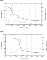
- the TGA curve of compound C-3 is depicted in figure 2 .
Landscapes
- Chemical & Material Sciences (AREA)
- Organic Chemistry (AREA)
- Metallurgy (AREA)
- Engineering & Computer Science (AREA)
- Materials Engineering (AREA)
- Mechanical Engineering (AREA)
- Chemical Kinetics & Catalysis (AREA)
- General Chemical & Material Sciences (AREA)
- Inorganic Chemistry (AREA)
- Chemical Vapour Deposition (AREA)
- Glass Compositions (AREA)
- Inorganic Insulating Materials (AREA)
- Formation Of Insulating Films (AREA)
Claims (14)
- Verfahren, umfassend das Überführen einer Verbindung der allgemeinen Formel (I) in den gasförmigen oder Aerosolzustand
Lm----M-Xn (I)
 R1, R2, R3 und R4 unabhängig voneinander eine Alkylgruppe, eine Arylgruppe oder eine Trialkylsilylgruppe sind,M Mn, Ni oder Co ist,X ein Ligand ist, der M koordiniert, wobei mindestens ein X ein neutral geladener Ligand ist,m 1, 2 oder 3 ist, undn mindestens 1 ist,wobei das Molekulargewicht der Verbindung der allgemeinen Formel (I) bis 1000 g/mol beträgt.
 - Verfahren nach Anspruch 1, wobei n mindestens 2 ist.
- Verfahren nach Anspruch 1 oder 2, wobei X und n ausgewählt werden, um die Anzahl von Valenzelektronen von M auf eine gerade Zahl einzustellen.
- Verfahren nach einem der Ansprüche 1 bis 3, wobei R1, R2, R3 und R4 Methyl oder Ethyl sind.
- Verfahren nach einem der Ansprüche 1 bis 4, wobei mindestens ein X ein Trialkylphosphin ist.
- Verfahren nach einem der Ansprüche 1 bis 5, wobei mindestens ein X CO ist.
- Verfahren nach einem der Ansprüche 1 bis 6, wobei M Co ist, und mindestens ein X NO ist.
- Verfahren nach einem der Ansprüche 1 bis 7, wobei mindestens ein X ein Ligand ist, der M über mindestens zwei neutrale oder anionische Stickstoffatome koordiniert.
- Verfahren nach einem der Ansprüche 1 bis 8, wobei mindestens ein X ein Ligand ist, der über ein Phosphoratom koordiniert.
- Verfahren nach einem der Ansprüche 1 bis 9, wobei die Verbindung der allgemeinen Formel (I) an die Oberfläche des festen Substrats chemisorbiert wird.
- Verfahren nach einem der Ansprüche 1 bis 10, wobei die abgeschiedene Verbindung der allgemeinen Formel (I) durch Entfernung aller Liganden L und X zersetzt wird.
- Verfahren nach Anspruch 11, wobei die abgeschiedene Verbindung der allgemeinen Formel (I) einem Reduktionsmittel ausgesetzt wird.
- Verfahren nach Anspruch 11 oder 12, wobei die Reihenfolge der Abscheidung der Verbindung der allgemeinen Formel (I) auf einem festen Substrat und des Zersetzens der abgeschiedenen Verbindung der allgemeinen Formel (I) mindestens zweimal vorgenommen wird.
- Verwendung einer Verbindung der allgemeinen Formel (I), wobei
R1, R2, R3 und R4 unabhängig voneinander eine Alkylgruppe, eine Arylgruppe oder eine Trialkylsilylgruppe sind,
M Mn, Ni oder Co ist,
X ein Ligand ist, der M koordiniert, wobei mindestens ein X ein neutral geladener Ligand ist,
m 1, 2 oder 3 ist, und
n mindestens 1 ist,
für ein Filmbildungsverfahren auf einem festen Substrat, wobei das Molekulargewicht der Verbindung der allgemeinen Formel (I) bis 1000 g/mol beträgt.
Applications Claiming Priority (2)
| Application Number | Priority Date | Filing Date | Title |
|---|---|---|---|
| EP15196031 | 2015-11-24 | ||
| PCT/EP2016/078099 WO2017089230A1 (en) | 2015-11-24 | 2016-11-18 | Process for the generation of thin inorganic films |
Publications (2)
| Publication Number | Publication Date |
|---|---|
| EP3380644A1 EP3380644A1 (de) | 2018-10-03 |
| EP3380644B1 true EP3380644B1 (de) | 2019-08-21 |
Family
ID=54780071
Family Applications (1)
| Application Number | Title | Priority Date | Filing Date |
|---|---|---|---|
| EP16798703.1A Active EP3380644B1 (de) | 2015-11-24 | 2016-11-18 | Verfahren zur erzeugung von dünnen anorganischen filmen |
Country Status (9)
| Country | Link |
|---|---|
| US (1) | US10801105B2 (de) |
| EP (1) | EP3380644B1 (de) |
| JP (1) | JP2018538442A (de) |
| KR (1) | KR102720323B1 (de) |
| CN (1) | CN108368606B (de) |
| IL (1) | IL259068B (de) |
| SG (1) | SG11201802577PA (de) |
| TW (1) | TWI721043B (de) |
| WO (1) | WO2017089230A1 (de) |
Families Citing this family (1)
| Publication number | Priority date | Publication date | Assignee | Title |
|---|---|---|---|---|
| TWI742022B (zh) * | 2015-11-30 | 2021-10-11 | 德商巴斯夫歐洲公司 | 生成金屬膜的方法 |
Family Cites Families (10)
| Publication number | Priority date | Publication date | Assignee | Title |
|---|---|---|---|---|
| US6273951B1 (en) * | 1999-06-16 | 2001-08-14 | Micron Technology, Inc. | Precursor mixtures for use in preparing layers on substrates |
| US7396949B2 (en) * | 2003-08-19 | 2008-07-08 | Denk Michael K | Class of volatile compounds for the deposition of thin films of metals and metal compounds |
| JP4975414B2 (ja) * | 2005-11-16 | 2012-07-11 | エーエスエム インターナショナル エヌ.ヴェー. | Cvd又はaldによる膜の堆積のための方法 |
| US20080248648A1 (en) * | 2007-04-06 | 2008-10-09 | Thompson David M | Deposition precursors for semiconductor applications |
| US20090226612A1 (en) | 2007-10-29 | 2009-09-10 | Satoko Ogawa | Alkaline earth metal containing precursor solutions |
| KR20100071463A (ko) * | 2008-12-19 | 2010-06-29 | 주식회사 유피케미칼 | 금속 박막 또는 금속 산화물 박막 증착용 유기금속 전구체 화합물 및 이를 이용한 박막 증착 방법 |
| WO2010125011A2 (de) * | 2009-04-28 | 2010-11-04 | Basf Se | Verfahren zur herstellung von halbleitenden schichten |
| US9018387B2 (en) * | 2010-06-11 | 2015-04-28 | Air Products And Chemicals, Inc. | Complexes of imidazole ligands |
| KR20140049988A (ko) * | 2011-05-13 | 2014-04-28 | 그린센터 캐나다 | 11 족 단일-금속 전구체 화합물 및 금속 증착에서의 이의 용도 |
| TW201533261A (zh) * | 2014-01-27 | 2015-09-01 | Basf Se | 產生薄無機膜之方法 |
-
2016
- 2016-11-18 CN CN201680068490.6A patent/CN108368606B/zh active Active
- 2016-11-18 SG SG11201802577PA patent/SG11201802577PA/en unknown
- 2016-11-18 IL IL259068A patent/IL259068B/en unknown
- 2016-11-18 US US15/775,856 patent/US10801105B2/en active Active
- 2016-11-18 EP EP16798703.1A patent/EP3380644B1/de active Active
- 2016-11-18 JP JP2018526852A patent/JP2018538442A/ja active Pending
- 2016-11-18 WO PCT/EP2016/078099 patent/WO2017089230A1/en not_active Ceased
- 2016-11-18 KR KR1020187014580A patent/KR102720323B1/ko active Active
- 2016-11-22 TW TW105138246A patent/TWI721043B/zh active
Non-Patent Citations (1)
| Title |
|---|
| None * |
Also Published As
| Publication number | Publication date |
|---|---|
| TWI721043B (zh) | 2021-03-11 |
| CN108368606B (zh) | 2021-04-13 |
| EP3380644A1 (de) | 2018-10-03 |
| CN108368606A (zh) | 2018-08-03 |
| SG11201802577PA (en) | 2018-06-28 |
| US20180320265A1 (en) | 2018-11-08 |
| JP2018538442A (ja) | 2018-12-27 |
| IL259068B (en) | 2022-07-01 |
| WO2017089230A1 (en) | 2017-06-01 |
| KR20180085728A (ko) | 2018-07-27 |
| US10801105B2 (en) | 2020-10-13 |
| IL259068A (en) | 2018-06-28 |
| TW201734247A (zh) | 2017-10-01 |
| KR102720323B1 (ko) | 2024-10-22 |
Similar Documents
| Publication | Publication Date | Title |
|---|---|---|
| US20180044357A1 (en) | Process for the generation of thin inorganic films | |
| US10106888B2 (en) | Process for the generation of thin inorganic films | |
| EP3532651A1 (de) | Verfahren zur erzeugung von dünnen siliciumhaltigen schichten | |
| EP3408273B1 (de) | Verfahren zur erzeugung von dünnen anorganischen filmen | |
| EP3380644B1 (de) | Verfahren zur erzeugung von dünnen anorganischen filmen | |
| EP3384063B1 (de) | Verfahren zur erzeugung von dünnen anorganischen filmen | |
| EP3507293B1 (de) | Verfahren zur erzeugung von dünnen anorganischen filmen | |
| EP3484901B1 (de) | Hapto-3-pentadienylkobalt oder -nickelvorläuferverbindungen und deren verwendung in dünnfilmabscheidungsprozessen | |
| EP3781577B1 (de) | Aluminium vorläufer und verfahren zur erzeugung von metallhaltigen filmen | |
| WO2017178400A1 (en) | Process for the generation of thin inorganic films |
Legal Events
| Date | Code | Title | Description |
|---|---|---|---|
| STAA | Information on the status of an ep patent application or granted ep patent |
Free format text: STATUS: UNKNOWN |
|
| STAA | Information on the status of an ep patent application or granted ep patent |
Free format text: STATUS: THE INTERNATIONAL PUBLICATION HAS BEEN MADE |
|
| PUAI | Public reference made under article 153(3) epc to a published international application that has entered the european phase |
Free format text: ORIGINAL CODE: 0009012 |
|
| STAA | Information on the status of an ep patent application or granted ep patent |
Free format text: STATUS: REQUEST FOR EXAMINATION WAS MADE |
|
| 17P | Request for examination filed |
Effective date: 20180625 |
|
| AK | Designated contracting states |
Kind code of ref document: A1 Designated state(s): AL AT BE BG CH CY CZ DE DK EE ES FI FR GB GR HR HU IE IS IT LI LT LU LV MC MK MT NL NO PL PT RO RS SE SI SK SM TR |
|
| AX | Request for extension of the european patent |
Extension state: BA ME |
|
| DAV | Request for validation of the european patent (deleted) | ||
| DAX | Request for extension of the european patent (deleted) | ||
| GRAP | Despatch of communication of intention to grant a patent |
Free format text: ORIGINAL CODE: EPIDOSNIGR1 |
|
| STAA | Information on the status of an ep patent application or granted ep patent |
Free format text: STATUS: GRANT OF PATENT IS INTENDED |
|
| INTG | Intention to grant announced |
Effective date: 20190320 |
|
| GRAS | Grant fee paid |
Free format text: ORIGINAL CODE: EPIDOSNIGR3 |
|
| GRAA | (expected) grant |
Free format text: ORIGINAL CODE: 0009210 |
|
| STAA | Information on the status of an ep patent application or granted ep patent |
Free format text: STATUS: THE PATENT HAS BEEN GRANTED |
|
| AK | Designated contracting states |
Kind code of ref document: B1 Designated state(s): AL AT BE BG CH CY CZ DE DK EE ES FI FR GB GR HR HU IE IS IT LI LT LU LV MC MK MT NL NO PL PT RO RS SE SI SK SM TR |
|
| REG | Reference to a national code |
Ref country code: GB Ref legal event code: FG4D |
|
| REG | Reference to a national code |
Ref country code: CH Ref legal event code: EP |
|
| REG | Reference to a national code |
Ref country code: DE Ref legal event code: R096 Ref document number: 602016019156 Country of ref document: DE |
|
| REG | Reference to a national code |
Ref country code: AT Ref legal event code: REF Ref document number: 1169850 Country of ref document: AT Kind code of ref document: T Effective date: 20190915 |
|
| REG | Reference to a national code |
Ref country code: IE Ref legal event code: FG4D |
|
| REG | Reference to a national code |
Ref country code: NL Ref legal event code: FP |
|
| REG | Reference to a national code |
Ref country code: LT Ref legal event code: MG4D |
|
| PG25 | Lapsed in a contracting state [announced via postgrant information from national office to epo] |
Ref country code: FI Free format text: LAPSE BECAUSE OF FAILURE TO SUBMIT A TRANSLATION OF THE DESCRIPTION OR TO PAY THE FEE WITHIN THE PRESCRIBED TIME-LIMIT Effective date: 20190821 Ref country code: NO Free format text: LAPSE BECAUSE OF FAILURE TO SUBMIT A TRANSLATION OF THE DESCRIPTION OR TO PAY THE FEE WITHIN THE PRESCRIBED TIME-LIMIT Effective date: 20191121 Ref country code: BG Free format text: LAPSE BECAUSE OF FAILURE TO SUBMIT A TRANSLATION OF THE DESCRIPTION OR TO PAY THE FEE WITHIN THE PRESCRIBED TIME-LIMIT Effective date: 20191121 Ref country code: SE Free format text: LAPSE BECAUSE OF FAILURE TO SUBMIT A TRANSLATION OF THE DESCRIPTION OR TO PAY THE FEE WITHIN THE PRESCRIBED TIME-LIMIT Effective date: 20190821 Ref country code: LT Free format text: LAPSE BECAUSE OF FAILURE TO SUBMIT A TRANSLATION OF THE DESCRIPTION OR TO PAY THE FEE WITHIN THE PRESCRIBED TIME-LIMIT Effective date: 20190821 Ref country code: PT Free format text: LAPSE BECAUSE OF FAILURE TO SUBMIT A TRANSLATION OF THE DESCRIPTION OR TO PAY THE FEE WITHIN THE PRESCRIBED TIME-LIMIT Effective date: 20191223 Ref country code: HR Free format text: LAPSE BECAUSE OF FAILURE TO SUBMIT A TRANSLATION OF THE DESCRIPTION OR TO PAY THE FEE WITHIN THE PRESCRIBED TIME-LIMIT Effective date: 20190821 |
|
| PG25 | Lapsed in a contracting state [announced via postgrant information from national office to epo] |
Ref country code: AL Free format text: LAPSE BECAUSE OF FAILURE TO SUBMIT A TRANSLATION OF THE DESCRIPTION OR TO PAY THE FEE WITHIN THE PRESCRIBED TIME-LIMIT Effective date: 20190821 Ref country code: RS Free format text: LAPSE BECAUSE OF FAILURE TO SUBMIT A TRANSLATION OF THE DESCRIPTION OR TO PAY THE FEE WITHIN THE PRESCRIBED TIME-LIMIT Effective date: 20190821 Ref country code: IS Free format text: LAPSE BECAUSE OF FAILURE TO SUBMIT A TRANSLATION OF THE DESCRIPTION OR TO PAY THE FEE WITHIN THE PRESCRIBED TIME-LIMIT Effective date: 20191221 Ref country code: GR Free format text: LAPSE BECAUSE OF FAILURE TO SUBMIT A TRANSLATION OF THE DESCRIPTION OR TO PAY THE FEE WITHIN THE PRESCRIBED TIME-LIMIT Effective date: 20191122 Ref country code: LV Free format text: LAPSE BECAUSE OF FAILURE TO SUBMIT A TRANSLATION OF THE DESCRIPTION OR TO PAY THE FEE WITHIN THE PRESCRIBED TIME-LIMIT Effective date: 20190821 Ref country code: ES Free format text: LAPSE BECAUSE OF FAILURE TO SUBMIT A TRANSLATION OF THE DESCRIPTION OR TO PAY THE FEE WITHIN THE PRESCRIBED TIME-LIMIT Effective date: 20190821 |
|
| REG | Reference to a national code |
Ref country code: AT Ref legal event code: MK05 Ref document number: 1169850 Country of ref document: AT Kind code of ref document: T Effective date: 20190821 |
|
| PG25 | Lapsed in a contracting state [announced via postgrant information from national office to epo] |
Ref country code: TR Free format text: LAPSE BECAUSE OF FAILURE TO SUBMIT A TRANSLATION OF THE DESCRIPTION OR TO PAY THE FEE WITHIN THE PRESCRIBED TIME-LIMIT Effective date: 20190821 |
|
| PG25 | Lapsed in a contracting state [announced via postgrant information from national office to epo] |
Ref country code: EE Free format text: LAPSE BECAUSE OF FAILURE TO SUBMIT A TRANSLATION OF THE DESCRIPTION OR TO PAY THE FEE WITHIN THE PRESCRIBED TIME-LIMIT Effective date: 20190821 Ref country code: DK Free format text: LAPSE BECAUSE OF FAILURE TO SUBMIT A TRANSLATION OF THE DESCRIPTION OR TO PAY THE FEE WITHIN THE PRESCRIBED TIME-LIMIT Effective date: 20190821 Ref country code: AT Free format text: LAPSE BECAUSE OF FAILURE TO SUBMIT A TRANSLATION OF THE DESCRIPTION OR TO PAY THE FEE WITHIN THE PRESCRIBED TIME-LIMIT Effective date: 20190821 Ref country code: PL Free format text: LAPSE BECAUSE OF FAILURE TO SUBMIT A TRANSLATION OF THE DESCRIPTION OR TO PAY THE FEE WITHIN THE PRESCRIBED TIME-LIMIT Effective date: 20190821 Ref country code: RO Free format text: LAPSE BECAUSE OF FAILURE TO SUBMIT A TRANSLATION OF THE DESCRIPTION OR TO PAY THE FEE WITHIN THE PRESCRIBED TIME-LIMIT Effective date: 20190821 |
|
| PG25 | Lapsed in a contracting state [announced via postgrant information from national office to epo] |
Ref country code: CZ Free format text: LAPSE BECAUSE OF FAILURE TO SUBMIT A TRANSLATION OF THE DESCRIPTION OR TO PAY THE FEE WITHIN THE PRESCRIBED TIME-LIMIT Effective date: 20190821 Ref country code: SK Free format text: LAPSE BECAUSE OF FAILURE TO SUBMIT A TRANSLATION OF THE DESCRIPTION OR TO PAY THE FEE WITHIN THE PRESCRIBED TIME-LIMIT Effective date: 20190821 Ref country code: IS Free format text: LAPSE BECAUSE OF FAILURE TO SUBMIT A TRANSLATION OF THE DESCRIPTION OR TO PAY THE FEE WITHIN THE PRESCRIBED TIME-LIMIT Effective date: 20200224 Ref country code: SM Free format text: LAPSE BECAUSE OF FAILURE TO SUBMIT A TRANSLATION OF THE DESCRIPTION OR TO PAY THE FEE WITHIN THE PRESCRIBED TIME-LIMIT Effective date: 20190821 |
|
| REG | Reference to a national code |
Ref country code: DE Ref legal event code: R097 Ref document number: 602016019156 Country of ref document: DE |
|
| REG | Reference to a national code |
Ref country code: CH Ref legal event code: PL |
|
| PLBE | No opposition filed within time limit |
Free format text: ORIGINAL CODE: 0009261 |
|
| STAA | Information on the status of an ep patent application or granted ep patent |
Free format text: STATUS: NO OPPOSITION FILED WITHIN TIME LIMIT |
|
| PG2D | Information on lapse in contracting state deleted |
Ref country code: IS |
|
| PG25 | Lapsed in a contracting state [announced via postgrant information from national office to epo] |
Ref country code: LI Free format text: LAPSE BECAUSE OF NON-PAYMENT OF DUE FEES Effective date: 20191130 Ref country code: CH Free format text: LAPSE BECAUSE OF NON-PAYMENT OF DUE FEES Effective date: 20191130 Ref country code: MC Free format text: LAPSE BECAUSE OF FAILURE TO SUBMIT A TRANSLATION OF THE DESCRIPTION OR TO PAY THE FEE WITHIN THE PRESCRIBED TIME-LIMIT Effective date: 20190821 Ref country code: LU Free format text: LAPSE BECAUSE OF NON-PAYMENT OF DUE FEES Effective date: 20191118 |
|
| 26N | No opposition filed |
Effective date: 20200603 |
|
| REG | Reference to a national code |
Ref country code: BE Ref legal event code: MM Effective date: 20191130 |
|
| PG25 | Lapsed in a contracting state [announced via postgrant information from national office to epo] |
Ref country code: SI Free format text: LAPSE BECAUSE OF FAILURE TO SUBMIT A TRANSLATION OF THE DESCRIPTION OR TO PAY THE FEE WITHIN THE PRESCRIBED TIME-LIMIT Effective date: 20190821 |
|
| PG25 | Lapsed in a contracting state [announced via postgrant information from national office to epo] |
Ref country code: BE Free format text: LAPSE BECAUSE OF NON-PAYMENT OF DUE FEES Effective date: 20191130 |
|
| PGFP | Annual fee paid to national office [announced via postgrant information from national office to epo] |
Ref country code: NL Payment date: 20201126 Year of fee payment: 5 |
|
| PGFP | Annual fee paid to national office [announced via postgrant information from national office to epo] |
Ref country code: IT Payment date: 20201120 Year of fee payment: 5 Ref country code: GB Payment date: 20201126 Year of fee payment: 5 |
|
| PG25 | Lapsed in a contracting state [announced via postgrant information from national office to epo] |
Ref country code: CY Free format text: LAPSE BECAUSE OF FAILURE TO SUBMIT A TRANSLATION OF THE DESCRIPTION OR TO PAY THE FEE WITHIN THE PRESCRIBED TIME-LIMIT Effective date: 20190821 |
|
| PG25 | Lapsed in a contracting state [announced via postgrant information from national office to epo] |
Ref country code: HU Free format text: LAPSE BECAUSE OF FAILURE TO SUBMIT A TRANSLATION OF THE DESCRIPTION OR TO PAY THE FEE WITHIN THE PRESCRIBED TIME-LIMIT; INVALID AB INITIO Effective date: 20161118 Ref country code: MT Free format text: LAPSE BECAUSE OF FAILURE TO SUBMIT A TRANSLATION OF THE DESCRIPTION OR TO PAY THE FEE WITHIN THE PRESCRIBED TIME-LIMIT Effective date: 20190821 |
|
| PG25 | Lapsed in a contracting state [announced via postgrant information from national office to epo] |
Ref country code: MK Free format text: LAPSE BECAUSE OF FAILURE TO SUBMIT A TRANSLATION OF THE DESCRIPTION OR TO PAY THE FEE WITHIN THE PRESCRIBED TIME-LIMIT Effective date: 20190821 |
|
| REG | Reference to a national code |
Ref country code: NL Ref legal event code: MM Effective date: 20211201 |
|
| GBPC | Gb: european patent ceased through non-payment of renewal fee |
Effective date: 20211118 |
|
| PG25 | Lapsed in a contracting state [announced via postgrant information from national office to epo] |
Ref country code: NL Free format text: LAPSE BECAUSE OF NON-PAYMENT OF DUE FEES Effective date: 20211201 |
|
| PG25 | Lapsed in a contracting state [announced via postgrant information from national office to epo] |
Ref country code: GB Free format text: LAPSE BECAUSE OF NON-PAYMENT OF DUE FEES Effective date: 20211118 |
|
| PG25 | Lapsed in a contracting state [announced via postgrant information from national office to epo] |
Ref country code: IT Free format text: LAPSE BECAUSE OF NON-PAYMENT OF DUE FEES Effective date: 20211118 |
|
| PGFP | Annual fee paid to national office [announced via postgrant information from national office to epo] |
Ref country code: DE Payment date: 20241128 Year of fee payment: 9 |
|
| PGFP | Annual fee paid to national office [announced via postgrant information from national office to epo] |
Ref country code: FR Payment date: 20241126 Year of fee payment: 9 |
|
| PGFP | Annual fee paid to national office [announced via postgrant information from national office to epo] |
Ref country code: IE Payment date: 20241119 Year of fee payment: 9 |