EP3378151B1 - Kommunikation mit gemeinsamer leitung in kaskadierten wechselrichtern - Google Patents
Kommunikation mit gemeinsamer leitung in kaskadierten wechselrichtern Download PDFInfo
- Publication number
- EP3378151B1 EP3378151B1 EP16866749.1A EP16866749A EP3378151B1 EP 3378151 B1 EP3378151 B1 EP 3378151B1 EP 16866749 A EP16866749 A EP 16866749A EP 3378151 B1 EP3378151 B1 EP 3378151B1
- Authority
- EP
- European Patent Office
- Prior art keywords
- switching
- switching units
- communication signal
- communication
- command signal
- Prior art date
- Legal status (The legal status is an assumption and is not a legal conclusion. Google has not performed a legal analysis and makes no representation as to the accuracy of the status listed.)
- Active
Links
- 238000004891 communication Methods 0.000 title claims description 107
- 238000000034 method Methods 0.000 claims description 28
- 230000004044 response Effects 0.000 claims description 6
- 230000005355 Hall effect Effects 0.000 claims description 4
- 238000005259 measurement Methods 0.000 claims description 4
- 238000004804 winding Methods 0.000 description 15
- 238000010586 diagram Methods 0.000 description 4
- 230000011664 signaling Effects 0.000 description 4
- 230000006978 adaptation Effects 0.000 description 3
- 230000005540 biological transmission Effects 0.000 description 3
- 238000001914 filtration Methods 0.000 description 3
- 238000012423 maintenance Methods 0.000 description 3
- 238000004519 manufacturing process Methods 0.000 description 3
- 239000004065 semiconductor Substances 0.000 description 3
- 238000004590 computer program Methods 0.000 description 2
- 238000005516 engineering process Methods 0.000 description 2
- 230000005669 field effect Effects 0.000 description 2
- 229910044991 metal oxide Inorganic materials 0.000 description 2
- 150000004706 metal oxides Chemical class 0.000 description 2
- 238000012544 monitoring process Methods 0.000 description 2
- 230000032683 aging Effects 0.000 description 1
- 230000003321 amplification Effects 0.000 description 1
- 238000004458 analytical method Methods 0.000 description 1
- 238000004364 calculation method Methods 0.000 description 1
- 239000003990 capacitor Substances 0.000 description 1
- 238000006243 chemical reaction Methods 0.000 description 1
- 239000004020 conductor Substances 0.000 description 1
- 230000008878 coupling Effects 0.000 description 1
- 238000010168 coupling process Methods 0.000 description 1
- 238000005859 coupling reaction Methods 0.000 description 1
- 230000001419 dependent effect Effects 0.000 description 1
- 230000006870 function Effects 0.000 description 1
- 239000000463 material Substances 0.000 description 1
- 238000003199 nucleic acid amplification method Methods 0.000 description 1
- 230000003287 optical effect Effects 0.000 description 1
- 230000000087 stabilizing effect Effects 0.000 description 1
- 230000007723 transport mechanism Effects 0.000 description 1
Images

Classifications
-
- H—ELECTRICITY
- H02—GENERATION; CONVERSION OR DISTRIBUTION OF ELECTRIC POWER
- H02M—APPARATUS FOR CONVERSION BETWEEN AC AND AC, BETWEEN AC AND DC, OR BETWEEN DC AND DC, AND FOR USE WITH MAINS OR SIMILAR POWER SUPPLY SYSTEMS; CONVERSION OF DC OR AC INPUT POWER INTO SURGE OUTPUT POWER; CONTROL OR REGULATION THEREOF
- H02M7/00—Conversion of AC power input into DC power output; Conversion of DC power input into AC power output
- H02M7/42—Conversion of DC power input into AC power output without possibility of reversal
- H02M7/44—Conversion of DC power input into AC power output without possibility of reversal by static converters
- H02M7/48—Conversion of DC power input into AC power output without possibility of reversal by static converters using discharge tubes with control electrode or semiconductor devices with control electrode
- H02M7/483—Converters with outputs that each can have more than two voltages levels
- H02M7/49—Combination of the output voltage waveforms of a plurality of converters
-
- H—ELECTRICITY
- H04—ELECTRIC COMMUNICATION TECHNIQUE
- H04B—TRANSMISSION
- H04B3/00—Line transmission systems
- H04B3/54—Systems for transmission via power distribution lines
- H04B3/542—Systems for transmission via power distribution lines the information being in digital form
-
- H—ELECTRICITY
- H02—GENERATION; CONVERSION OR DISTRIBUTION OF ELECTRIC POWER
- H02M—APPARATUS FOR CONVERSION BETWEEN AC AND AC, BETWEEN AC AND DC, OR BETWEEN DC AND DC, AND FOR USE WITH MAINS OR SIMILAR POWER SUPPLY SYSTEMS; CONVERSION OF DC OR AC INPUT POWER INTO SURGE OUTPUT POWER; CONTROL OR REGULATION THEREOF
- H02M7/00—Conversion of AC power input into DC power output; Conversion of DC power input into AC power output
- H02M7/42—Conversion of DC power input into AC power output without possibility of reversal
- H02M7/44—Conversion of DC power input into AC power output without possibility of reversal by static converters
- H02M7/48—Conversion of DC power input into AC power output without possibility of reversal by static converters using discharge tubes with control electrode or semiconductor devices with control electrode
- H02M7/483—Converters with outputs that each can have more than two voltages levels
- H02M7/4835—Converters with outputs that each can have more than two voltages levels comprising two or more cells, each including a switchable capacitor, the capacitors having a nominal charge voltage which corresponds to a given fraction of the input voltage, and the capacitors being selectively connected in series to determine the instantaneous output voltage
-
- H—ELECTRICITY
- H02—GENERATION; CONVERSION OR DISTRIBUTION OF ELECTRIC POWER
- H02M—APPARATUS FOR CONVERSION BETWEEN AC AND AC, BETWEEN AC AND DC, OR BETWEEN DC AND DC, AND FOR USE WITH MAINS OR SIMILAR POWER SUPPLY SYSTEMS; CONVERSION OF DC OR AC INPUT POWER INTO SURGE OUTPUT POWER; CONTROL OR REGULATION THEREOF
- H02M7/00—Conversion of AC power input into DC power output; Conversion of DC power input into AC power output
- H02M7/42—Conversion of DC power input into AC power output without possibility of reversal
- H02M7/44—Conversion of DC power input into AC power output without possibility of reversal by static converters
- H02M7/48—Conversion of DC power input into AC power output without possibility of reversal by static converters using discharge tubes with control electrode or semiconductor devices with control electrode
- H02M7/53—Conversion of DC power input into AC power output without possibility of reversal by static converters using discharge tubes with control electrode or semiconductor devices with control electrode using devices of a triode or transistor type requiring continuous application of a control signal
- H02M7/537—Conversion of DC power input into AC power output without possibility of reversal by static converters using discharge tubes with control electrode or semiconductor devices with control electrode using devices of a triode or transistor type requiring continuous application of a control signal using semiconductor devices only, e.g. single switched pulse inverters
- H02M7/5387—Conversion of DC power input into AC power output without possibility of reversal by static converters using discharge tubes with control electrode or semiconductor devices with control electrode using devices of a triode or transistor type requiring continuous application of a control signal using semiconductor devices only, e.g. single switched pulse inverters in a bridge configuration
-
- H—ELECTRICITY
- H04—ELECTRIC COMMUNICATION TECHNIQUE
- H04B—TRANSMISSION
- H04B3/00—Line transmission systems
- H04B3/54—Systems for transmission via power distribution lines
-
- H—ELECTRICITY
- H04—ELECTRIC COMMUNICATION TECHNIQUE
- H04B—TRANSMISSION
- H04B2203/00—Indexing scheme relating to line transmission systems
- H04B2203/54—Aspects of powerline communications not already covered by H04B3/54 and its subgroups
- H04B2203/5429—Applications for powerline communications
- H04B2203/5445—Local network
Definitions
- the invention disclosed herein relates to communication in power inverter systems. More precisely, it relates to a method of communicating with controlled cascaded switching units arranged to receive an input power and to deliver a combined output voltage waveform and alternating current to for example a power grid.
- Switching units are widely used in power inverter systems for changing direct current (DC) to alternating current (AC).
- DC direct current
- AC alternating current
- a plurality of switching units can be combined in series to form a combined, multilevel output voltage waveform.
- the switching units may be electrically connected in cascade configuration to provide a desired combined output voltage waveform and AC.
- the individual operation of the switching units may e.g. be effectuated by means of a switch control circuitry, which requires transmission of information between the units of the system.
- control signals are transferred between a central adaptation unit and switching units by means of a wireless communication channel.
- US Patent Application No. US2015/0163074 discloses a system including a power system coupled to a power bus, and a power line communication gateway coupled in series with the power bus.
- European Patent Application No. EP2725678 discloses a power line communication device capable of keeping attenuation of electric power of a control signal to a minimum.
- the power line communication device includes a communication unit, and a switch unit.
- An object of at least some of the embodiments of the present invention is to provide methods in a power inverter system, switching units and a central unit, and in particular to provide an improved alternative to the above techniques.
- the invention provides methods, devices and a system with the features of the independent claims.
- the dependent claims define advantageous embodiments.
- a method in a power inverter system comprises a plurality of switching units that are electrically connected to each other in cascade configuration.
- Each of the switching units is adapted to receive a respective input power.
- each of the switching units is operable in an inverter mode in which the switching units are individually switched so as to produce a combined output voltage waveform, and a communication mode in which the switching units are switched so as to produce a communication signal.
- the combined output voltage from the switching units and the communication signal may be transferred on the same wire or line.
- at least some of the switching units are in the inverter mode switched in response to switching commands of a command signal and/or other types of information provided by e.g. a data signal.
- at least one of the switching units is operated in the communication mode during a period of time defined by two consecutive switching commands of the command signal.
- a method in a central unit comprises the steps of receiving, via a common line adapted to transferring both power and communication data, a communication signal generated by a switching unit operating in a communication mode, calculating a command signal based on the received communication signal, and outputting the command signal via the common line.
- the switching unit is one of a plurality of switching units electrically connected in cascade configuration, wherein each one of the plurality of switching units is adapted to receive a respective input DC power and operable in an inverter mode and a communication mode.
- the switching units are individually switched in response to switching commands of the command signal so as to produce a combined output voltage waveform and current transferred on the common line.
- the switching units are switched to produce the communication signal.
- a power inverter system comprising a plurality of switching units electrically connected in cascade configuration.
- Each one of the plurality of switching units is adapted to receive a respective input DC power and operable in an inverter mode in which the switching units are individually switched in response to switching commands of a command signal so as to produce a combined output voltage and current waveform transferred on a common line.
- the switching units are operable, between two consecutive switching commands of the command signal, in a communication mode in which the switching units are switched so as to produce a communication signal, wherein the communication signal is transmitted in the common line.
- a central unit which is adapted to receive, via a common line, a communication signal generated by a switching unit according to the third aspect.
- the communication signal is processed by a processor adapted to calculate a command signal based on the received communication signal.
- the central unit further comprises a communication interface through which the command signal is output to the common line.
- a system comprising a power inverter system according to the third aspect and a central unit according to the fourth aspect.
- the multilevel output voltage waveform can be built up and designed so there are “silent” periods where the voltage is relatively constant and has a relatively low harmonic content. Those "silent” periods may be located between two consecutive switching events of the switching units. These “silent” periods may be utilized for transmitting a superimposed communication signal on the combined output and with a relatively low harmonic content (i.e., noise) that otherwise may be caused by level transients.
- the communication signal may be achieved by switching one or several of the switching units while letting the remaining switching units be silent, i.e., remain in its present state as the communication signal is generated.
- the switching units may, in other words, be considered to operate in two different modes - the inverter mode generating the combined multilevel output voltage and current waveform and at the same time be able to receive the communication signal and the communication mode generating the communication signal.
- each or at least some of the switching units may be switched based on switching commands of the command signal so as to form a desired multilevel output voltage and current waveform and simultaneously be able to receive communication data and commands from the central unit.
- the period defined by two mutually adjacent switching commands may be referred to as a silent period of the multilevel output AC, as the output may be relatively stable or constant during this period.
- the output voltage may during this silent period have a relatively low noise, which is particularly advantageous in connection with signaling as a relatively low level of noise may reduce the need for filtering and amplification of the communication signal.
- one or several of the switching units may be operated in the communication mode, in which they may be switched a plurality of times to generate a superimposed communication signal.
- the switching units may be operated at a relatively low switching frequency in the inverter mode as compared to commonly known topologies where a high frequency is used and desired in order to reduce the size of filter components.
- a lower switching frequency may allow for reduced switching losses and hence an inverter with increased efficiency.
- the command signal may e.g. comprise a state command causing a switching unit to output or receive power, and preferably to output a voltage at a certain level (positive, zero, negative or voltages there between). Additionally, or alternatively, the state command may cause the switching unit to cease outputting power and voltage.
- the command signal may also comprise further or alternative commands causing the switching units to output any combination of two or more of a positive voltage, a negative voltage, zero voltage and voltages there between. This also applies when operated in the communication mode, wherein the switching unit may alternate between any of the above mentioned outputs.
- Each one of the plurality of switching units may be adapted to receive, via the common line, a communication signal generated by another switching unit or the central unit.
- the communication signal may be processed by a processor adapted to calculate a command signal based on the received communication signal.
- the communication signal may comprise information relating to voltages or currents in the system, such as the level of DC input to the switching unit or the level of output AC, and other parameters relating to e.g. temperature, capability and performance of the switching unit.
- the central unit may use information in the communication signal when determining or calculating the command signal.
- Information regarding the current state or operation of the inverter system or its input may hence be used as feedback for controlling the inverter system.
- the central unit may further be adapted to receive information representing at least one of frequency, phase, amplitude and harmonics of a required AC, such as e.g. a grid AC, and to receive information, via the communication signal, representing at least one of input current and input voltage to each one, or at least some, of the switching units. Based on the received information, the switching units may be individually controlled such that the combined output from the plurality of switching units produces a voltage and current waveform matching the required voltage and current waveform.
- a required AC such as e.g. a grid AC
- the individual control of the switching units is particularly relevant for applications and systems wherein the respective input DC power varies over time and/or is difficult to predict. This may be the case in for e.g. photovoltaic (PV) elements or solar panels, wherein the output power may be determined by a non-linear relationship between voltage and current of the DC input. Events like a passing shadow, or differences in panel performance due to pollution, differential aging or differences during manufacturing may hinder an array of panels as whole to operate at its peak efficiency point.
- PV photovoltaic
- the present aspects provide a solution wherein each panel may be connected to a respective switching unit that is cascaded and can be individually operated in response to the input DC power from each one of the panels. Information about the input DC power may be transferred by the communication signal to the central unit, wherein a micro-controller or processor may be provided to generate a suitable command signal indicating a switching pattern to be used by the switching units.
- the present aspects further allow for individual input DC power sources, such as e.g. solar panels, to be monitored.
- Monitoring energy production i.e. produced input DC power, voltage and/or current
- the monitoring may be accomplished by means of the communication signal, which may be transmitted to the central unit for further analysis.
- the communication signal further comprises an identifier indicating an identity of the switching unit producing the communication signal.
- the central unit may thereby be able to distinguish between individual switching units and hence to adapt the command signal accordingly.
- each one of the switching units may comprise a sensor adapted to receive the command signal and/or the communication signal.
- the sensor may, in case of a current being the main information carrier for, e.g. comprise means for sensing changes in current, for example a signal transformer, a current transformer, a shunt resistor or a Hall-effect measurement device.
- one or several of the power stage transistors on-resistance or conduction voltage drop may be used for sensing the communication signal.
- the communication signal may, in case of the main information carrier being a voltage, be determined by means of a sensing device detecting changes in voltage.
- a sensing device may e.g. utilize resistive voltage dividers combined with AC coupling in the form of e.g. capacitors.
- the senor may comprise a common mode inductor having a core with a first winding and a second winding, wherein the first winding and the second winding forms a differential pair of conductors arranged to convey a differential communication signal.
- a common mode inductor may comprise a third winding arranged to extend along at least a portion of the first winding and a fourth winding arranged to extend along at least a portion of the second winding.
- the third winding and the fourth winding may be inductively coupled to the first winding and the second winding, respectively, and be connected in series with each other so as to provide a sensor signal induced by the differential communication signal in the first winding and the second winding.
- the central unit may comprise communication interface adapted to output the command signal and/or to receive the communication signal.
- the communication interface may e.g. comprise a transmitter having a switching unit which may be similarly configured as the one already discussed. Such a switching unit may be adapted to generate a signal, such as a command signal, in the silent periods between two switching commands.
- the communication interface may according to some embodiments comprise a sensor, such as e.g. a transformer, resistor, a Hall-effect measurement device, or a transistor as mentioned above, for receiving and determining the communication signal. Further, a common mode inductor with an additional sensor winding as described above may be used.
- a switching unit may, in the context of the present application, refer to an electric component capable of receiving input DC power and producing a multilevel output of at least two different voltage levels or more.
- the switching unit may also be referred to as a DC/AC converter and may e.g. be formed of an H-bridge or half bridge converter.
- the H-bridge converter may e.g. comprise four metal oxide semiconductor field effect transistors (MOSFETs) or any other type of semiconductor switch or transistor.
- the half bridge converter may e.g. comprise two transistors.
- the present aspects may be embodied as computer-readable instructions for controlling a programmable computer in such manner that it performs the method outlined above.
- Such instructions may be distributed in the form of a computer-program product comprising a computer-readable medium storing the instructions.
- the instructions may be loaded in a micro-controller or control device such as for example FPGA, ASIC, CPU, MCU of the central unit.
- FIG. 1 shows a power inverter system 100 and a central unit 130 according to an embodiment.
- the power inverter system 100 comprises a plurality of switching units, such as e.g. H-bridge converters 110, each being arranged to be supplied with an input DC power source voltage V DC from a respective source, such as e.g. a photovoltaic element (not shown in figure 1 ).
- the H-bridge converters 110 may be cascaded to produce a multilevel output voltage V OUT , which may be fed via the common line 120 to the central unit 130.
- the central unit 130 may be adapted to output a voltage V AC matching e.g. the grid alternating voltage and feed an output current I AC to e.g. the grid.
- each H-bridge converter 110 may be integrated in e.g. a junction box of the respective panel.
- a central adaptation unit may be provided (not shown) for adapting the combined multilevel output voltage waveform such that a voltage similar to the grid voltage V AC is output from the system.
- the central adaptation unit may e.g. be realized by means of an inductor for taking up a possible voltage mismatch between the system and the grid voltage V AC , and to provide an impedance which may be used for controlling and stabilizing the output current.
- Each one of the switching units 110 may be adapted to operate in a communication mode wherein silent periods of the combined output voltage waveform V OUT , i.e., in periods where no switching occurs, are utilized for generating a communication signal.
- the communication signal may be superimposed on the combined output voltage waveform V OUT and transmitted via the common line 120 to the central unit 130.
- the central unit 130 may be adapted to generate a command signal for controlling the operation of the H-bridges 110.
- the command signal may be generated in a similar way as the communication signal, i.e., by means of a switching unit (not shown) switching during a silent period of the combined output voltage waveform V OUT .
- the communication signal may e.g. comprise information indicating a current level or voltage level of the input V DC at the respective switching unit 110. Further, the communication signal may comprise an identifier indicating the identity of the switching unit 110 generating the communication signal. This information and/or other information may be used at the central unit 130 for controlling the operation of the power inverter system 100.
- FIG 2 shows an exemplifying embodiment of a switching unit 110 according to the embodiment discussed with reference to figure 1 . More specifically, a circuit diagram of an H-bridge converter 21, comprising four switching elements Q1, Q2, Q3, Q4 in the form of four metal oxide semiconductor field effect transistors (MOSFETs) Q1, Q2, Q3, Q4, is shown.
- MOSFETs metal oxide semiconductor field effect transistors
- any other appropriate switching element may be used, such as insulated gate bipolar transistors (IGBTs), or bipolar junction transistors (BJTs).
- IGBTs insulated gate bipolar transistors
- BJTs bipolar junction transistors
- the drain D1 of the first transistor Q1 and the drain D2 of the second transistor Q2 may be electrically connected to a positive pole 15 of an input DC power source, such as e.g. photovoltaic panel (not shown), while the sources S1 and S2 of the respective first and second transistors Q1 and Q2 may be electrically connected to the drains D4 and D3 of the fourth and third transistors Q4, Q3, respectively.
- the sources S3 and S4 of the third and fourth transistors Q4, Q3 may be electrically connected to a negative pole 43 of the input DC power source.
- the source S1 of the first transistor Q1 may be electrically connected to the drain D4 of the fourth transistor Q4 at a first output terminal 52, whereas the source S2 of the second transistor Q2 is electrically connected to the drain D3 of the third transistor Q3 at a second output terminal 54.
- the gate terminals G1, G2, G3, G4 of the four transistors Q1, Q2, Q3, Q4 may be electrically connected to a switch control circuitry 60 adapted to control the MOSFETs Q1, Q2, Q3, Q4 by supplying a gate voltage to their respective gates G1, G2, G3, G4.
- the switch control circuitry may comprise a micro-controller or computing unit 60, e.g. mounted on a printed circuit board (not shown) along with the switching unit 110.
- the micro-controller or computing unit 60 may also be connected to e.g. current and/or voltage meters (not shown) providing the micro-controller with information on the input voltage and current, the combined output from the power inverter system 100 and/or a required AC voltage waveform or current.
- the micro-controller 60 may be adapted to operate the switching units 110 in the inverter mode in such manner that the combined output from the plurality of switching units 110 of the power inverter system 100 produces a combined multilevel voltage waveform matching the required voltage waveform. Further, the micro-controller 60 may operate the switching unit 110 in the communication mode, wherein the switching unit 110, in a silent period between two consecutive switching events of any of the plurality of switching units 110, may produce a communication signal. This may be achieved by means of the micro-controller 60, which may operate the switching units Q1, Q2, Q3, Q4 so as to generate output forming the desired communication signal.
- the micro-controller 60 may be configured to receive the command signal from the central unit (not shown in figure 2 ) and operate the switching unit accordingly in the inverter mode.
- the command signal may e.g. be received by means of a receiving circuitry or sensor comprising e.g. an AC coupled transformer, a current transformer, a shunt resistor, a Hall-effect measurement device, or a conduction voltage drop over a transistor (not shown).
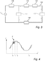
- FIG. 3 shows a power inverter system and a central unit that may be similarly configured as the power inverter system and central unit discussed with reference to figures 1 and 2 .
- the power inverter system 100 may comprise a plurality of cascaded switching units 110 that are connected to a central unit 130 that may be adapted to receive the communication signal generated by the power inverter system 100 and to transmit a command signal controlling operation of the power inverter system 100.
- further components such as e.g. a terminator 122 for reducing reflections of the communication signal in the common line 120.
- Further components may be e.g. a filter 126 for filtering the output before it is output to e.g. the grid, and a filter 124 that is arranged in the central unit 130 so as to filter the command signal.
- the filters 124, 126 may be structurally integrated in the central unit 130.
- the communication signal and the command signal are represented by a dashed line, wherein arrows are provided to schematically indicate the path of the signals during operation of the power inverter system 100 and central unit 130.
- the communication signal and the command signal may circulate from the switching units 110 of the power inverter system 100, via the common line 120 to the central unit 130, from which the command signal (which may be based in the communication signal) may be output/returned to the switching units 110.
- the combined output voltage waveform V OUT may be transmitted in the same common line 120 as the communication signal and/or the command signal, but may be further transmitted as an output AC V AC to e.g. the grid.
- FIG 4 is a diagram illustrating a combined multilevel output voltage waveform V OUT from a power inverter system that may be similarly configured as the power inverter systems described with reference to any one of figures 1 to 3 .
- the combined output voltage waveform V OUT is indicated as a voltage, U (vertical axis) as a function of time t (horizontal axis).
- cascaded switching units are used to generate a combined multilevel output voltage waveform V OUT matching a desired sinusoidal voltage waveform V AC after filtering.
- the switching events of the switching units are indicated by t 0 , t 1 , ..., t n on the horizontal axis and may correspond to switching commands of the command signal, causing the switching units to switch between different output levels.
- the silent periods that can be used for signaling are schematically represented by the flat steps between two consecutive switching commands or switching events t n , t n+1 .
- the communication signal is generated during silent period T between switching events t 0 and t 1 .
- the signal may e.g. be generated by operating one of the switching units in the communication mode during that period, i.e., by switching the switching unit a plurality of times between t 0 and t 1 .
- the communication signal may hence be superimposed on the combined multilevel output.
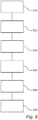
- FIG 5 there is shown a schematic outline of a method according to an embodiment of the present invention, wherein a power inverter system comprising plurality of switching units in cascade configuration is controlled so as to generate a communication signal and a combined multilevel output voltage waveform and AC on the same line.
- the method will in this example be discussed with reference to a power inverter system and a central unit similarly configured as the embodiments discussed in connection with figures 1 to 4 .
- the method comprises operating 510 at least some of the switching units in an inverter mode in which the switching units are individually switched in response to switching commands of a command signal so as to produce a combined output voltage waveform transferred on the common line. Further, the method comprises operating 520, between two consecutive switching commands of the command signal, at least one switching unit in a communication mode in which the switching unit is switched so as to produce the communication signal, wherein the communication signal is transmitted in the common line.
- the communication signal in the common line may be received 530 and processed 540 by e.g. a micro-controller, resulting in the calculation 550 of a command signal that may be based on the received information.
- the command signal may be output 560, via the common line, to the inverter system.
- computer-readable media may comprise computer storage media and communication media.
- computer storage media includes both volatile and non-volatile, removable and non-removable media implemented in any method or technology for storage of information such as computer readable instructions, data structures, program modules or other data.
- Computer storage media includes, but is not limited to, RAM, ROM, EEPROM, flash memory or other memory technology, CD-ROM, digital versatile disks (DVD) or other optical disk storage, magnetic cassettes, magnetic tape, magnetic disk storage or other magnetic storage devices.
- communication media typically embodies computer readable instructions, data structures, program modules or other data in a modulated data signal such as a carrier wave or other transport mechanism and includes any information delivery media.
Landscapes
- Engineering & Computer Science (AREA)
- Power Engineering (AREA)
- Computer Networks & Wireless Communication (AREA)
- Signal Processing (AREA)
- Inverter Devices (AREA)
- Supply And Distribution Of Alternating Current (AREA)
Claims (16)
- Verfahren in einem Wechselrichtersystem (100), umfassend:Ausgeben eines Befehlssignals von einer Zentraleinheit (130), wobei das Befehlssignal Schaltbefehle umfasst;Empfangen des Befehlssignals an einer Vielzahl an Schalteinheiten (110), wobei jede Schalteinheit Schaltelemente (Q1, Q2, Q3, Q4) und eine Schaltsteuerung, die die Schaltelemente (Q1, Q2, Q3, Q4) steuert, umfasst, welche in Kaskadenkonfiguration elektrisch verbunden und zum Empfangen einer jeweiligen Eingangsgleichspannung (VDC) angepasst sind;Betreiben mindestens einiger der Vielzahl an Schalteinheiten (110) in einem Wechselrichtermodus, in dem die Schalteinheiten (110) einzeln, durch Umschalten ihrer jeweiligen Schaltelemente (Q1), (Q2), (Q3), (Q4), geschaltet werden um einen kombinierten Ausgangswechselstrom (VOUT) zu erzeugen;Ausgeben des kombinierten Wechselstromausgangs an eine gemeinsame Leitung (120);dadurch gekennzeichnet, dass das Verfahren ferner umfasst:zwischen zwei aufeinanderfolgenden Schaltbefehlen des Befehlssignals, Betreiben von mindestens einer der Schalteinheiten (110) in einem Kommunikationsmodus, in dem die Schalteinheit durch Umschalten ihrer jeweiligen Schaltelemente (Q1), (Q2), (Q3), (Q4) geschaltet wird, um ein Kommunikationssignal zu erzeugen;Ausgeben des Kommunikationssignals an die gemeinsame Leitung (120); undEmpfangen des Kommunikationssignals an der Zentraleinheit (130).
- Verfahren nach Anspruch 1, wobei das Kommunikationssignal, das an der Zentraleinheit (130) empfangen wird, als Rückmeldung zur Erzeugung des Befehlssignals verwendet wird.
- Verfahren nach Anspruch 1 oder 2, wobei das Kommunikationssignal eine Kennung umfasst, die eine Identität der Schalteinheit anzeigt, die das Kommunikationssignal erzeugt.
- Verfahren nach einem der vorhergehenden Ansprüche, wobei die Schalteinheiten (110) zwischen einer Vielzahl an Ausgangsspannungspegeln im Wechselrichtermodus und / oder im Kommunikationsmodus geschaltet werden.
- Verfahren nach Anspruch 4, wobei die Schalteinheiten (110) zwischen einem positiven Spannungspegel und einem negativen Spannungspegel im Wechselrichtermodus und / oder Kommunikationsmodus geschaltet werden.
- Verfahren nach Anspruch 4, wobei die Schalteinheiten (110) zwischen einem positiven Spannungspegel, einem Nullspannungspegel und einem negativen Spannungspegel im Wechselrichtermodus und / oder im Kommunikationsmodus geschaltet werden.
- Verfahren nach einem der vorhergehenden Ansprüche, wobei die kombinierte Ausgangswechselspannung eine mehrstufige Spannungswellenform ist und worin jeder Pegel der mehrstufigen Spannungswellenform durch eine Ausgabe von einer der Schalteinheiten (110) oder eine Summe von Ausgaben von der Vielzahl der Schalteinheiten (110) gebildet wird.
- Verfahren nach einem der vorhergehenden Ansprüche, wobei die Schalteinheiten (110) einzeln so geschaltet werden, dass eine Zeitspanne zwischen zwei aufeinanderfolgenden Schaltereignissen oder den Schalteinheiten (110) es erlaubt, dass eine vorbestimmte Datenmenge vom Wechselrichtersystem (100) ausgegeben wird.
- Das Verfahren nach einem der vorhergehenden Ansprüche, ferner umfassend das Bestimmen des Kommunikationssignals durch Messen einer Spannungsdifferenz oder elektrischen Stroms.
- Wechselrichtersystem (100), umfassend eine Zentraleinheit (130) und Vielzahl an Schalteinheiten (110) die in Kaskadenkonfiguration elektrisch verbunden sind, wobei:die Zentraleinheit (130) angepasst ist, über eine gemeinsame Leitung (120) ein Kommunikationssignal zu empfangen und an die gemeinsame Leitung (120) ein Befehlssignal, das Schaltbefehle umfasst, auszugeben; und wobeiund wobei jede der Vielzahl an Schalteinheiten Schaltelemente (Q1, Q2, Q3, Q4) und eine Schaltsteuerung, die die Schaltelemente (Q1, Q2, Q3, Q4) steuert, umfasst und ist:angepasst, um eine jeweilige Eingangsgleichstromleistung zu empfangen;in einem Wechselrichtermodus betreibbar, in dem die Schalteinheiten (110) einzeln, durch Umschalten ihrer jeweiligen Schaltelemente (Q1), (Q2), (Q3), (Q4), als Antwort auf die Schaltbefehle des Befehlssignals, geschaltet werden um einen kombinierten Ausgangswechselstrom (VOUT) zu erzeugen, der in die gemeinsame Leitung (120) übertragen wird;dadurch gekennzeichnet, dass jede der Vielzahl an Schalteinheiten (110) ferner ist:
zwischen zwei aufeinanderfolgenden Schaltbefehlen des Befehlssignals in einem Kommunikationsmodus betreibbar, in dem die Schalteinheiten (110), durch Umschalten ihrer jeweiligen Schaltelemente (Q1), (Q2), (Q3), (Q4), geschaltet werden, um ein Kommunikationssignal zu erzeugen, wobei das Kommunikationssignal in der gemeinsamen Leitung (120) übertragen wird. - Wechselrichtersystem (100), nach Anspruch 10, wobei die Schalteinheiten H-Brückenwandler sind.
- Wechselrichtersystem nach Anspruch 10 oder 11, wobei jede Schalteinheit einen Sensor umfasst, der zum Empfangen des Befehlssignals angepasst ist.
- Wechselrichtersystem (100) nach Anspruch 11 oder 12, wobei jede der Vielzahl an Schalteinheiten so angepasst ist, dass sie betriebsmäßig mit einer jeweiligen Photovoltaikplatte, die zur Bereitstellung der Eingangsgleichstromleistung angepasst ist, verbunden ist.
- Wechselrichtersystem (100) nach einem der Ansprüche 10 bis 13, wobei die Zentraleinheit (130) ferner umfasst:einen Prozessor, der angepasst ist, um das Befehlssignal basierend auf dem empfangenen Kommunikationssignal zu berechnen; undeine Kommunikationsschnittstelle, die angepasst ist, um das Befehlssignal an die gemeinsame Leitung (120) auszugeben.
- Wechselrichtersystem (100) nach einem der Ansprüche 11 bis 14, ferner umfassend einen Sensor, der zur Bestimmung des Kommunikationssignals angepasst ist.
- Wechselrichtersystem (100) nach Anspruch 15, wobei der Sensor mindestens eines umfasst: einen gekoppelten Wechselstromtransformator, einen Stromwandler, einen Nebenschlusswiderstand, eine Hall-Effekt-Messvorrichtung und einen Leitungstransistor.
Applications Claiming Priority (2)
| Application Number | Priority Date | Filing Date | Title |
|---|---|---|---|
| SE1551492A SE539911C2 (en) | 2015-11-18 | 2015-11-18 | Common line communication in cascaded inverters |
| PCT/SE2016/051113 WO2017086862A1 (en) | 2015-11-18 | 2016-11-11 | Common line communication in cascaded inverters |
Publications (4)
| Publication Number | Publication Date |
|---|---|
| EP3378151A1 EP3378151A1 (de) | 2018-09-26 |
| EP3378151A4 EP3378151A4 (de) | 2019-06-19 |
| EP3378151B1 true EP3378151B1 (de) | 2020-08-26 |
| EP3378151B8 EP3378151B8 (de) | 2020-11-18 |
Family
ID=58719093
Family Applications (1)
| Application Number | Title | Priority Date | Filing Date |
|---|---|---|---|
| EP16866749.1A Active EP3378151B8 (de) | 2015-11-18 | 2016-11-11 | Kommunikation mit gemeinsamer leitung in kaskadierten wechselrichtern |
Country Status (8)
| Country | Link |
|---|---|
| US (1) | US10833602B2 (de) |
| EP (1) | EP3378151B8 (de) |
| JP (1) | JP6567772B2 (de) |
| CN (1) | CN108886329B (de) |
| AU (1) | AU2016354859B2 (de) |
| ES (1) | ES2833954T3 (de) |
| SE (1) | SE539911C2 (de) |
| WO (1) | WO2017086862A1 (de) |
Cited By (1)
| Publication number | Priority date | Publication date | Assignee | Title |
|---|---|---|---|---|
| EP4468613A4 (de) * | 2022-04-27 | 2025-05-21 | Hoymiles Power Electronics Inc. | Stromleitungsträgerkommunikationsvorrichtung, -verfahren und -system |
Families Citing this family (1)
| Publication number | Priority date | Publication date | Assignee | Title |
|---|---|---|---|---|
| EP4040623A1 (de) * | 2021-02-04 | 2022-08-10 | VARTA Microbattery GmbH | Modulares batteriespeichersystem mit wiederaufladbaren energiespeichermodulen und verfahren zum betreiben des batteriespeichersystems |
Family Cites Families (15)
| Publication number | Priority date | Publication date | Assignee | Title |
|---|---|---|---|---|
| JP4423157B2 (ja) * | 2004-10-06 | 2010-03-03 | キヤノン株式会社 | 電力線通信装置およびその制御方法 |
| KR100825323B1 (ko) | 2007-03-05 | 2008-04-28 | 엘에스산전 주식회사 | 단위 셀 역률 동일 제어 장치를 가지는 캐스케이드 방식을이용한 멀티레벨 인버터 및 그 제어방법 |
| US20080283118A1 (en) * | 2007-05-17 | 2008-11-20 | Larankelo, Inc. | Photovoltaic ac inverter mount and interconnect |
| EP2454795A4 (de) | 2009-07-14 | 2016-09-21 | Enphase Energy Inc | Verfahren und vorrichtung zur identifikation umgeordneter verteilter generatorkomponenten |
| US8860242B1 (en) * | 2009-12-31 | 2014-10-14 | Solarbridge Technologies, Inc. | Power-line communication coupling |
| KR101047511B1 (ko) * | 2010-03-10 | 2011-07-07 | 최인숙 | 전력전송구간을 분할하여 데이터 신호를 전송하는 전력선 통신방법 |
| AU2012282686B2 (en) | 2011-07-11 | 2015-11-05 | Sinewatts, Inc. | Systems and methods for solar photovoltaic energy collection and conversion |
| US20140161201A1 (en) * | 2011-07-28 | 2014-06-12 | Panasonic Corporation | Power line communication device, solar power generation system, power line communication method, and power line communication program |
| JP2013048523A (ja) | 2011-08-29 | 2013-03-07 | Toyota Industries Corp | 車両用充電システム |
| CA2845664C (en) * | 2011-08-31 | 2019-04-23 | Optistring Technologies Ab | Dc-ac inverter for photovoltaic systems |
| JP2013135478A (ja) | 2011-12-24 | 2013-07-08 | Sumitomo Electric Ind Ltd | 給電装置及び通信方法 |
| US9257837B2 (en) * | 2013-01-04 | 2016-02-09 | Solarcity Corporation | Power balancing in a multi-phase system |
| EP2773036B1 (de) | 2013-02-27 | 2016-02-24 | Optistring Technologies AB | Verfahren zur Gleichstrom-Wechselstrom-Umwandlung |
| US9564835B2 (en) * | 2013-03-15 | 2017-02-07 | Sunpower Corporation | Inverter communications using output signal |
| EP2852069A1 (de) * | 2013-09-24 | 2015-03-25 | ABB Research Ltd. | System zum Übertragen und Empfangen eines Stromleitungskommunikationssignals über den Leistungsbus eines elektronischen Stromwandlers |
-
2015
- 2015-11-18 SE SE1551492A patent/SE539911C2/en not_active IP Right Cessation
-
2016
- 2016-11-11 ES ES16866749T patent/ES2833954T3/es active Active
- 2016-11-11 US US15/777,545 patent/US10833602B2/en not_active Expired - Fee Related
- 2016-11-11 JP JP2018524422A patent/JP6567772B2/ja not_active Expired - Fee Related
- 2016-11-11 WO PCT/SE2016/051113 patent/WO2017086862A1/en not_active Ceased
- 2016-11-11 EP EP16866749.1A patent/EP3378151B8/de active Active
- 2016-11-11 AU AU2016354859A patent/AU2016354859B2/en not_active Ceased
- 2016-11-11 CN CN201680066878.2A patent/CN108886329B/zh not_active Expired - Fee Related
Non-Patent Citations (1)
| Title |
|---|
| None * |
Cited By (1)
| Publication number | Priority date | Publication date | Assignee | Title |
|---|---|---|---|---|
| EP4468613A4 (de) * | 2022-04-27 | 2025-05-21 | Hoymiles Power Electronics Inc. | Stromleitungsträgerkommunikationsvorrichtung, -verfahren und -system |
Also Published As
| Publication number | Publication date |
|---|---|
| ES2833954T3 (es) | 2021-06-16 |
| AU2016354859A1 (en) | 2018-05-24 |
| WO2017086862A1 (en) | 2017-05-26 |
| WO2017086862A8 (en) | 2018-11-15 |
| AU2016354859B2 (en) | 2019-08-15 |
| SE539911C2 (en) | 2018-01-09 |
| SE1551492A1 (en) | 2017-05-19 |
| EP3378151B8 (de) | 2020-11-18 |
| CN108886329A (zh) | 2018-11-23 |
| EP3378151A4 (de) | 2019-06-19 |
| JP2018538772A (ja) | 2018-12-27 |
| CN108886329B (zh) | 2020-10-02 |
| JP6567772B2 (ja) | 2019-08-28 |
| US20180337614A1 (en) | 2018-11-22 |
| US10833602B2 (en) | 2020-11-10 |
| EP3378151A1 (de) | 2018-09-26 |
Similar Documents
| Publication | Publication Date | Title |
|---|---|---|
| EP3378070B1 (de) | Gleichtaktinduktivität und verfahren zum messen eines gegentakt-kommunikationssignals in einer gleichtaktinduktivität | |
| EP3171503B1 (de) | Selbsttestsystem für kaskadierten multilevel-wandler und selbsttestverfahren dafür | |
| JPWO2018016106A1 (ja) | Dc/dcコンバータ | |
| AU2019232828A1 (en) | Active filter topology for cascaded inverters | |
| CN114123205B (zh) | 谐波补偿系统及其相位校正方法与装置 | |
| EP3378151B1 (de) | Kommunikation mit gemeinsamer leitung in kaskadierten wechselrichtern | |
| JP5640541B2 (ja) | 系統連系インバータ装置 | |
| CN104836566B (zh) | 传输ask信号的电子电路和方法 | |
| JP2017112827A (ja) | 信号伝達回路 | |
| KR101898975B1 (ko) | 전기 공급망을 위한 모듈러 변환기 시스템 | |
| US20120127763A1 (en) | Electric power supply system comprising power modules coupled in parallel | |
| JP6558298B2 (ja) | 信号伝達回路、及び、信号伝達システム | |
| Bulakh et al. | A multichannel power supply for high power magnetrons | |
| CN105186890A (zh) | 交流传动车辆无变压器拓扑结构及控制直流输出的方法 |
Legal Events
| Date | Code | Title | Description |
|---|---|---|---|
| STAA | Information on the status of an ep patent application or granted ep patent |
Free format text: STATUS: THE INTERNATIONAL PUBLICATION HAS BEEN MADE |
|
| PUAI | Public reference made under article 153(3) epc to a published international application that has entered the european phase |
Free format text: ORIGINAL CODE: 0009012 |
|
| STAA | Information on the status of an ep patent application or granted ep patent |
Free format text: STATUS: REQUEST FOR EXAMINATION WAS MADE |
|
| 17P | Request for examination filed |
Effective date: 20180615 |
|
| AK | Designated contracting states |
Kind code of ref document: A1 Designated state(s): AL AT BE BG CH CY CZ DE DK EE ES FI FR GB GR HR HU IE IS IT LI LT LU LV MC MK MT NL NO PL PT RO RS SE SI SK SM TR |
|
| AX | Request for extension of the european patent |
Extension state: BA ME |
|
| DAV | Request for validation of the european patent (deleted) | ||
| DAX | Request for extension of the european patent (deleted) | ||
| A4 | Supplementary search report drawn up and despatched |
Effective date: 20190517 |
|
| RIC1 | Information provided on ipc code assigned before grant |
Ipc: H04B 3/54 20060101ALI20190513BHEP Ipc: H02M 7/483 20070101AFI20190513BHEP Ipc: H02M 7/49 20070101ALI20190513BHEP Ipc: H02J 3/38 20060101ALN20190513BHEP |
|
| REG | Reference to a national code |
Ref country code: DE Ref legal event code: R079 Ref document number: 602016042953 Country of ref document: DE Free format text: PREVIOUS MAIN CLASS: H02M0007490000 Ipc: H02M0007483000 |
|
| GRAP | Despatch of communication of intention to grant a patent |
Free format text: ORIGINAL CODE: EPIDOSNIGR1 |
|
| STAA | Information on the status of an ep patent application or granted ep patent |
Free format text: STATUS: GRANT OF PATENT IS INTENDED |
|
| RIC1 | Information provided on ipc code assigned before grant |
Ipc: H04B 3/54 20060101ALI20200227BHEP Ipc: H02M 7/483 20070101AFI20200227BHEP Ipc: H02J 3/38 20060101ALN20200227BHEP Ipc: H02M 7/49 20070101ALI20200227BHEP |
|
| RIC1 | Information provided on ipc code assigned before grant |
Ipc: H04B 3/54 20060101ALI20200310BHEP Ipc: H02M 7/483 20070101AFI20200310BHEP Ipc: H02J 3/38 20060101ALN20200310BHEP Ipc: H02M 7/49 20070101ALI20200310BHEP |
|
| INTG | Intention to grant announced |
Effective date: 20200323 |
|
| GRAS | Grant fee paid |
Free format text: ORIGINAL CODE: EPIDOSNIGR3 |
|
| GRAA | (expected) grant |
Free format text: ORIGINAL CODE: 0009210 |
|
| STAA | Information on the status of an ep patent application or granted ep patent |
Free format text: STATUS: THE PATENT HAS BEEN GRANTED |
|
| AK | Designated contracting states |
Kind code of ref document: B1 Designated state(s): AL AT BE BG CH CY CZ DE DK EE ES FI FR GB GR HR HU IE IS IT LI LT LU LV MC MK MT NL NO PL PT RO RS SE SI SK SM TR |
|
| REG | Reference to a national code |
Ref country code: GB Ref legal event code: FG4D |
|
| REG | Reference to a national code |
Ref country code: CH Ref legal event code: EP |
|
| REG | Reference to a national code |
Ref country code: AT Ref legal event code: REF Ref document number: 1307351 Country of ref document: AT Kind code of ref document: T Effective date: 20200915 |
|
| REG | Reference to a national code |
Ref country code: IE Ref legal event code: FG4D |
|
| REG | Reference to a national code |
Ref country code: DE Ref legal event code: R096 Ref document number: 602016042953 Country of ref document: DE |
|
| REG | Reference to a national code |
Ref country code: DE Ref legal event code: R081 Ref document number: 602016042953 Country of ref document: DE Owner name: MARICI HOLDINGS THE NETHERLANDS B.V., NL Free format text: FORMER OWNER: ABB SCHWEIZ AG, BADEN, CH |
|
| REG | Reference to a national code |
Ref country code: CH Ref legal event code: PK Free format text: BERICHTIGUNG B8 |
|
| RAP2 | Party data changed (patent owner data changed or rights of a patent transferred) |
Owner name: MARICI HOLDINGS THE NETHERLANDS B.V. |
|
| REG | Reference to a national code |
Ref country code: LT Ref legal event code: MG4D |
|
| PG25 | Lapsed in a contracting state [announced via postgrant information from national office to epo] |
Ref country code: LT Free format text: LAPSE BECAUSE OF FAILURE TO SUBMIT A TRANSLATION OF THE DESCRIPTION OR TO PAY THE FEE WITHIN THE PRESCRIBED TIME-LIMIT Effective date: 20200826 Ref country code: FI Free format text: LAPSE BECAUSE OF FAILURE TO SUBMIT A TRANSLATION OF THE DESCRIPTION OR TO PAY THE FEE WITHIN THE PRESCRIBED TIME-LIMIT Effective date: 20200826 Ref country code: SE Free format text: LAPSE BECAUSE OF FAILURE TO SUBMIT A TRANSLATION OF THE DESCRIPTION OR TO PAY THE FEE WITHIN THE PRESCRIBED TIME-LIMIT Effective date: 20200826 Ref country code: HR Free format text: LAPSE BECAUSE OF FAILURE TO SUBMIT A TRANSLATION OF THE DESCRIPTION OR TO PAY THE FEE WITHIN THE PRESCRIBED TIME-LIMIT Effective date: 20200826 Ref country code: PT Free format text: LAPSE BECAUSE OF FAILURE TO SUBMIT A TRANSLATION OF THE DESCRIPTION OR TO PAY THE FEE WITHIN THE PRESCRIBED TIME-LIMIT Effective date: 20201228 Ref country code: BG Free format text: LAPSE BECAUSE OF FAILURE TO SUBMIT A TRANSLATION OF THE DESCRIPTION OR TO PAY THE FEE WITHIN THE PRESCRIBED TIME-LIMIT Effective date: 20201126 Ref country code: GR Free format text: LAPSE BECAUSE OF FAILURE TO SUBMIT A TRANSLATION OF THE DESCRIPTION OR TO PAY THE FEE WITHIN THE PRESCRIBED TIME-LIMIT Effective date: 20201127 Ref country code: NO Free format text: LAPSE BECAUSE OF FAILURE TO SUBMIT A TRANSLATION OF THE DESCRIPTION OR TO PAY THE FEE WITHIN THE PRESCRIBED TIME-LIMIT Effective date: 20201126 |
|
| REG | Reference to a national code |
Ref country code: NL Ref legal event code: MP Effective date: 20200826 |
|
| REG | Reference to a national code |
Ref country code: AT Ref legal event code: MK05 Ref document number: 1307351 Country of ref document: AT Kind code of ref document: T Effective date: 20200826 |
|
| PG25 | Lapsed in a contracting state [announced via postgrant information from national office to epo] |
Ref country code: PL Free format text: LAPSE BECAUSE OF FAILURE TO SUBMIT A TRANSLATION OF THE DESCRIPTION OR TO PAY THE FEE WITHIN THE PRESCRIBED TIME-LIMIT Effective date: 20200826 Ref country code: RS Free format text: LAPSE BECAUSE OF FAILURE TO SUBMIT A TRANSLATION OF THE DESCRIPTION OR TO PAY THE FEE WITHIN THE PRESCRIBED TIME-LIMIT Effective date: 20200826 Ref country code: NL Free format text: LAPSE BECAUSE OF FAILURE TO SUBMIT A TRANSLATION OF THE DESCRIPTION OR TO PAY THE FEE WITHIN THE PRESCRIBED TIME-LIMIT Effective date: 20200826 Ref country code: LV Free format text: LAPSE BECAUSE OF FAILURE TO SUBMIT A TRANSLATION OF THE DESCRIPTION OR TO PAY THE FEE WITHIN THE PRESCRIBED TIME-LIMIT Effective date: 20200826 Ref country code: IS Free format text: LAPSE BECAUSE OF FAILURE TO SUBMIT A TRANSLATION OF THE DESCRIPTION OR TO PAY THE FEE WITHIN THE PRESCRIBED TIME-LIMIT Effective date: 20201226 |
|
| PG25 | Lapsed in a contracting state [announced via postgrant information from national office to epo] |
Ref country code: DK Free format text: LAPSE BECAUSE OF FAILURE TO SUBMIT A TRANSLATION OF THE DESCRIPTION OR TO PAY THE FEE WITHIN THE PRESCRIBED TIME-LIMIT Effective date: 20200826 Ref country code: CZ Free format text: LAPSE BECAUSE OF FAILURE TO SUBMIT A TRANSLATION OF THE DESCRIPTION OR TO PAY THE FEE WITHIN THE PRESCRIBED TIME-LIMIT Effective date: 20200826 Ref country code: RO Free format text: LAPSE BECAUSE OF FAILURE TO SUBMIT A TRANSLATION OF THE DESCRIPTION OR TO PAY THE FEE WITHIN THE PRESCRIBED TIME-LIMIT Effective date: 20200826 Ref country code: EE Free format text: LAPSE BECAUSE OF FAILURE TO SUBMIT A TRANSLATION OF THE DESCRIPTION OR TO PAY THE FEE WITHIN THE PRESCRIBED TIME-LIMIT Effective date: 20200826 Ref country code: SM Free format text: LAPSE BECAUSE OF FAILURE TO SUBMIT A TRANSLATION OF THE DESCRIPTION OR TO PAY THE FEE WITHIN THE PRESCRIBED TIME-LIMIT Effective date: 20200826 |
|
| REG | Reference to a national code |
Ref country code: DE Ref legal event code: R097 Ref document number: 602016042953 Country of ref document: DE |
|
| PG25 | Lapsed in a contracting state [announced via postgrant information from national office to epo] |
Ref country code: AL Free format text: LAPSE BECAUSE OF FAILURE TO SUBMIT A TRANSLATION OF THE DESCRIPTION OR TO PAY THE FEE WITHIN THE PRESCRIBED TIME-LIMIT Effective date: 20200826 Ref country code: AT Free format text: LAPSE BECAUSE OF FAILURE TO SUBMIT A TRANSLATION OF THE DESCRIPTION OR TO PAY THE FEE WITHIN THE PRESCRIBED TIME-LIMIT Effective date: 20200826 |
|
| REG | Reference to a national code |
Ref country code: ES Ref legal event code: FG2A Ref document number: 2833954 Country of ref document: ES Kind code of ref document: T3 Effective date: 20210616 |
|
| PG25 | Lapsed in a contracting state [announced via postgrant information from national office to epo] |
Ref country code: MC Free format text: LAPSE BECAUSE OF FAILURE TO SUBMIT A TRANSLATION OF THE DESCRIPTION OR TO PAY THE FEE WITHIN THE PRESCRIBED TIME-LIMIT Effective date: 20200826 Ref country code: SK Free format text: LAPSE BECAUSE OF FAILURE TO SUBMIT A TRANSLATION OF THE DESCRIPTION OR TO PAY THE FEE WITHIN THE PRESCRIBED TIME-LIMIT Effective date: 20200826 |
|
| REG | Reference to a national code |
Ref country code: CH Ref legal event code: PL |
|
| PLBE | No opposition filed within time limit |
Free format text: ORIGINAL CODE: 0009261 |
|
| STAA | Information on the status of an ep patent application or granted ep patent |
Free format text: STATUS: NO OPPOSITION FILED WITHIN TIME LIMIT |
|
| GBPC | Gb: european patent ceased through non-payment of renewal fee |
Effective date: 20201126 |
|
| PG25 | Lapsed in a contracting state [announced via postgrant information from national office to epo] |
Ref country code: LU Free format text: LAPSE BECAUSE OF NON-PAYMENT OF DUE FEES Effective date: 20201111 |
|
| 26N | No opposition filed |
Effective date: 20210527 |
|
| REG | Reference to a national code |
Ref country code: BE Ref legal event code: MM Effective date: 20201130 |
|
| PG25 | Lapsed in a contracting state [announced via postgrant information from national office to epo] |
Ref country code: CH Free format text: LAPSE BECAUSE OF NON-PAYMENT OF DUE FEES Effective date: 20201130 Ref country code: LI Free format text: LAPSE BECAUSE OF NON-PAYMENT OF DUE FEES Effective date: 20201130 Ref country code: SI Free format text: LAPSE BECAUSE OF FAILURE TO SUBMIT A TRANSLATION OF THE DESCRIPTION OR TO PAY THE FEE WITHIN THE PRESCRIBED TIME-LIMIT Effective date: 20200826 |
|
| PG25 | Lapsed in a contracting state [announced via postgrant information from national office to epo] |
Ref country code: IE Free format text: LAPSE BECAUSE OF NON-PAYMENT OF DUE FEES Effective date: 20201111 Ref country code: FR Free format text: LAPSE BECAUSE OF NON-PAYMENT OF DUE FEES Effective date: 20201130 |
|
| PG25 | Lapsed in a contracting state [announced via postgrant information from national office to epo] |
Ref country code: GB Free format text: LAPSE BECAUSE OF NON-PAYMENT OF DUE FEES Effective date: 20201126 |
|
| PG25 | Lapsed in a contracting state [announced via postgrant information from national office to epo] |
Ref country code: IS Free format text: LAPSE BECAUSE OF FAILURE TO SUBMIT A TRANSLATION OF THE DESCRIPTION OR TO PAY THE FEE WITHIN THE PRESCRIBED TIME-LIMIT Effective date: 20201226 Ref country code: TR Free format text: LAPSE BECAUSE OF FAILURE TO SUBMIT A TRANSLATION OF THE DESCRIPTION OR TO PAY THE FEE WITHIN THE PRESCRIBED TIME-LIMIT Effective date: 20200826 Ref country code: MT Free format text: LAPSE BECAUSE OF FAILURE TO SUBMIT A TRANSLATION OF THE DESCRIPTION OR TO PAY THE FEE WITHIN THE PRESCRIBED TIME-LIMIT Effective date: 20200826 Ref country code: CY Free format text: LAPSE BECAUSE OF FAILURE TO SUBMIT A TRANSLATION OF THE DESCRIPTION OR TO PAY THE FEE WITHIN THE PRESCRIBED TIME-LIMIT Effective date: 20200826 |
|
| PG25 | Lapsed in a contracting state [announced via postgrant information from national office to epo] |
Ref country code: MK Free format text: LAPSE BECAUSE OF FAILURE TO SUBMIT A TRANSLATION OF THE DESCRIPTION OR TO PAY THE FEE WITHIN THE PRESCRIBED TIME-LIMIT Effective date: 20200826 |
|
| PG25 | Lapsed in a contracting state [announced via postgrant information from national office to epo] |
Ref country code: BE Free format text: LAPSE BECAUSE OF NON-PAYMENT OF DUE FEES Effective date: 20201130 |
|
| PGFP | Annual fee paid to national office [announced via postgrant information from national office to epo] |
Ref country code: ES Payment date: 20230125 Year of fee payment: 7 |
|
| PGFP | Annual fee paid to national office [announced via postgrant information from national office to epo] |
Ref country code: IT Payment date: 20230120 Year of fee payment: 7 Ref country code: DE Payment date: 20230123 Year of fee payment: 7 |
|
| REG | Reference to a national code |
Ref country code: DE Ref legal event code: R119 Ref document number: 602016042953 Country of ref document: DE |
|
| PG25 | Lapsed in a contracting state [announced via postgrant information from national office to epo] |
Ref country code: DE Free format text: LAPSE BECAUSE OF NON-PAYMENT OF DUE FEES Effective date: 20240601 |
|
| PG25 | Lapsed in a contracting state [announced via postgrant information from national office to epo] |
Ref country code: DE Free format text: LAPSE BECAUSE OF NON-PAYMENT OF DUE FEES Effective date: 20240601 |
|
| PG25 | Lapsed in a contracting state [announced via postgrant information from national office to epo] |
Ref country code: IT Free format text: LAPSE BECAUSE OF NON-PAYMENT OF DUE FEES Effective date: 20231111 |
|
| PG25 | Lapsed in a contracting state [announced via postgrant information from national office to epo] |
Ref country code: IT Free format text: LAPSE BECAUSE OF NON-PAYMENT OF DUE FEES Effective date: 20231111 |
|
| REG | Reference to a national code |
Ref country code: ES Ref legal event code: FD2A Effective date: 20250103 |
|
| PG25 | Lapsed in a contracting state [announced via postgrant information from national office to epo] |
Ref country code: ES Free format text: LAPSE BECAUSE OF NON-PAYMENT OF DUE FEES Effective date: 20231112 |
|
| PG25 | Lapsed in a contracting state [announced via postgrant information from national office to epo] |
Ref country code: ES Free format text: LAPSE BECAUSE OF NON-PAYMENT OF DUE FEES Effective date: 20231112 |