EP3376548A1 - Light-emitting diode device and manufacturing method therefor - Google Patents
Light-emitting diode device and manufacturing method therefor Download PDFInfo
- Publication number
- EP3376548A1 EP3376548A1 EP16863637.1A EP16863637A EP3376548A1 EP 3376548 A1 EP3376548 A1 EP 3376548A1 EP 16863637 A EP16863637 A EP 16863637A EP 3376548 A1 EP3376548 A1 EP 3376548A1
- Authority
- EP
- European Patent Office
- Prior art keywords
- encapsulant
- led
- ring
- led device
- substrate
- Prior art date
- Legal status (The legal status is an assumption and is not a legal conclusion. Google has not performed a legal analysis and makes no representation as to the accuracy of the status listed.)
- Withdrawn
Links
- 238000004519 manufacturing process Methods 0.000 title abstract description 34
- 239000008393 encapsulating agent Substances 0.000 claims abstract description 200
- 230000004888 barrier function Effects 0.000 claims abstract description 167
- 239000000758 substrate Substances 0.000 claims description 118
- 230000007423 decrease Effects 0.000 claims description 6
- 238000013461 design Methods 0.000 abstract description 11
- 239000000084 colloidal system Substances 0.000 description 51
- 239000012790 adhesive layer Substances 0.000 description 35
- 238000000034 method Methods 0.000 description 30
- 238000005520 cutting process Methods 0.000 description 25
- 230000000694 effects Effects 0.000 description 15
- 239000000463 material Substances 0.000 description 13
- 230000008569 process Effects 0.000 description 11
- 230000008859 change Effects 0.000 description 8
- 239000004033 plastic Substances 0.000 description 7
- 238000004806 packaging method and process Methods 0.000 description 6
- 238000012360 testing method Methods 0.000 description 5
- 229910017623 MgSi2 Inorganic materials 0.000 description 4
- 229910052751 metal Inorganic materials 0.000 description 4
- 239000002184 metal Substances 0.000 description 4
- 239000000203 mixture Substances 0.000 description 4
- 239000011342 resin composition Substances 0.000 description 4
- 239000000919 ceramic Substances 0.000 description 3
- 238000005516 engineering process Methods 0.000 description 3
- 238000003475 lamination Methods 0.000 description 3
- 239000002245 particle Substances 0.000 description 3
- 229910002971 CaTiO3 Inorganic materials 0.000 description 2
- 229910052688 Gadolinium Inorganic materials 0.000 description 2
- VYPSYNLAJGMNEJ-UHFFFAOYSA-N Silicium dioxide Chemical compound O=[Si]=O VYPSYNLAJGMNEJ-UHFFFAOYSA-N 0.000 description 2
- 239000005084 Strontium aluminate Substances 0.000 description 2
- GWEVSGVZZGPLCZ-UHFFFAOYSA-N Titan oxide Chemical compound O=[Ti]=O GWEVSGVZZGPLCZ-UHFFFAOYSA-N 0.000 description 2
- -1 Y(P Inorganic materials 0.000 description 2
- XLOMVQKBTHCTTD-UHFFFAOYSA-N Zinc monoxide Chemical compound [Zn]=O XLOMVQKBTHCTTD-UHFFFAOYSA-N 0.000 description 2
- MCMNRKCIXSYSNV-UHFFFAOYSA-N Zirconium dioxide Chemical compound O=[Zr]=O MCMNRKCIXSYSNV-UHFFFAOYSA-N 0.000 description 2
- 229910052788 barium Inorganic materials 0.000 description 2
- 230000008901 benefit Effects 0.000 description 2
- 239000007795 chemical reaction product Substances 0.000 description 2
- 238000000576 coating method Methods 0.000 description 2
- 239000003086 colorant Substances 0.000 description 2
- 238000011161 development Methods 0.000 description 2
- 239000003822 epoxy resin Substances 0.000 description 2
- 230000002349 favourable effect Effects 0.000 description 2
- 230000017525 heat dissipation Effects 0.000 description 2
- 229910052909 inorganic silicate Inorganic materials 0.000 description 2
- 239000010410 layer Substances 0.000 description 2
- 238000012986 modification Methods 0.000 description 2
- 230000004048 modification Effects 0.000 description 2
- 238000000465 moulding Methods 0.000 description 2
- 238000006303 photolysis reaction Methods 0.000 description 2
- 230000015843 photosynthesis, light reaction Effects 0.000 description 2
- 229920000647 polyepoxide Polymers 0.000 description 2
- 239000000047 product Substances 0.000 description 2
- 229920005989 resin Polymers 0.000 description 2
- 239000011347 resin Substances 0.000 description 2
- 229920002050 silicone resin Polymers 0.000 description 2
- 238000005476 soldering Methods 0.000 description 2
- 229910016010 BaAl2 Inorganic materials 0.000 description 1
- 229910020440 K2SiF6 Inorganic materials 0.000 description 1
- 229910007536 Li2Si2 Inorganic materials 0.000 description 1
- 229910010092 LiAlO2 Inorganic materials 0.000 description 1
- BQCADISMDOOEFD-UHFFFAOYSA-N Silver Chemical compound [Ag] BQCADISMDOOEFD-UHFFFAOYSA-N 0.000 description 1
- 229910003080 TiO4 Inorganic materials 0.000 description 1
- 230000004913 activation Effects 0.000 description 1
- 229910052925 anhydrite Inorganic materials 0.000 description 1
- OSGAYBCDTDRGGQ-UHFFFAOYSA-L calcium sulfate Chemical compound [Ca+2].[O-]S([O-])(=O)=O OSGAYBCDTDRGGQ-UHFFFAOYSA-L 0.000 description 1
- 229910052923 celestite Inorganic materials 0.000 description 1
- 239000011248 coating agent Substances 0.000 description 1
- 229910052681 coesite Inorganic materials 0.000 description 1
- 239000000571 coke Substances 0.000 description 1
- 239000000356 contaminant Substances 0.000 description 1
- 229910052802 copper Inorganic materials 0.000 description 1
- 229910052906 cristobalite Inorganic materials 0.000 description 1
- 229910003460 diamond Inorganic materials 0.000 description 1
- 239000010432 diamond Substances 0.000 description 1
- 230000005496 eutectics Effects 0.000 description 1
- 239000011521 glass Substances 0.000 description 1
- 125000001475 halogen functional group Chemical group 0.000 description 1
- 230000006872 improvement Effects 0.000 description 1
- 238000002347 injection Methods 0.000 description 1
- 239000007924 injection Substances 0.000 description 1
- 229910052749 magnesium Inorganic materials 0.000 description 1
- 230000003340 mental effect Effects 0.000 description 1
- 238000000197 pyrolysis Methods 0.000 description 1
- 230000005855 radiation Effects 0.000 description 1
- 238000002310 reflectometry Methods 0.000 description 1
- 238000007788 roughening Methods 0.000 description 1
- 238000007650 screen-printing Methods 0.000 description 1
- SBIBMFFZSBJNJF-UHFFFAOYSA-N selenium;zinc Chemical compound [Se]=[Zn] SBIBMFFZSBJNJF-UHFFFAOYSA-N 0.000 description 1
- 239000000377 silicon dioxide Substances 0.000 description 1
- 229910052709 silver Inorganic materials 0.000 description 1
- 239000004332 silver Substances 0.000 description 1
- 238000002791 soaking Methods 0.000 description 1
- 229910000679 solder Inorganic materials 0.000 description 1
- 239000007787 solid Substances 0.000 description 1
- 239000000243 solution Substances 0.000 description 1
- 238000005507 spraying Methods 0.000 description 1
- 229910052682 stishovite Inorganic materials 0.000 description 1
- 229910052712 strontium Inorganic materials 0.000 description 1
- 238000013519 translation Methods 0.000 description 1
- 229910052905 tridymite Inorganic materials 0.000 description 1
- 229910052720 vanadium Inorganic materials 0.000 description 1
- 229910019901 yttrium aluminum garnet Inorganic materials 0.000 description 1
- 229910000164 yttrium(III) phosphate Inorganic materials 0.000 description 1
Images


Classifications
-
- H—ELECTRICITY
- H01—ELECTRIC ELEMENTS
- H01L—SEMICONDUCTOR DEVICES NOT COVERED BY CLASS H10
- H01L33/00—Semiconductor devices having potential barriers specially adapted for light emission; Processes or apparatus specially adapted for the manufacture or treatment thereof or of parts thereof; Details thereof
- H01L33/48—Semiconductor devices having potential barriers specially adapted for light emission; Processes or apparatus specially adapted for the manufacture or treatment thereof or of parts thereof; Details thereof characterised by the semiconductor body packages
- H01L33/58—Optical field-shaping elements
- H01L33/60—Reflective elements
-
- H—ELECTRICITY
- H01—ELECTRIC ELEMENTS
- H01L—SEMICONDUCTOR DEVICES NOT COVERED BY CLASS H10
- H01L2224/00—Indexing scheme for arrangements for connecting or disconnecting semiconductor or solid-state bodies and methods related thereto as covered by H01L24/00
- H01L2224/01—Means for bonding being attached to, or being formed on, the surface to be connected, e.g. chip-to-package, die-attach, "first-level" interconnects; Manufacturing methods related thereto
- H01L2224/42—Wire connectors; Manufacturing methods related thereto
- H01L2224/47—Structure, shape, material or disposition of the wire connectors after the connecting process
- H01L2224/48—Structure, shape, material or disposition of the wire connectors after the connecting process of an individual wire connector
- H01L2224/4805—Shape
- H01L2224/4809—Loop shape
- H01L2224/48091—Arched
-
- H—ELECTRICITY
- H01—ELECTRIC ELEMENTS
- H01L—SEMICONDUCTOR DEVICES NOT COVERED BY CLASS H10
- H01L2933/00—Details relating to devices covered by the group H01L33/00 but not provided for in its subgroups
- H01L2933/0008—Processes
- H01L2933/0033—Processes relating to semiconductor body packages
-
- H—ELECTRICITY
- H01—ELECTRIC ELEMENTS
- H01L—SEMICONDUCTOR DEVICES NOT COVERED BY CLASS H10
- H01L2933/00—Details relating to devices covered by the group H01L33/00 but not provided for in its subgroups
- H01L2933/0008—Processes
- H01L2933/0033—Processes relating to semiconductor body packages
- H01L2933/005—Processes relating to semiconductor body packages relating to encapsulations
-
- H—ELECTRICITY
- H01—ELECTRIC ELEMENTS
- H01L—SEMICONDUCTOR DEVICES NOT COVERED BY CLASS H10
- H01L2933/00—Details relating to devices covered by the group H01L33/00 but not provided for in its subgroups
- H01L2933/0008—Processes
- H01L2933/0033—Processes relating to semiconductor body packages
- H01L2933/0058—Processes relating to semiconductor body packages relating to optical field-shaping elements
-
- H—ELECTRICITY
- H01—ELECTRIC ELEMENTS
- H01L—SEMICONDUCTOR DEVICES NOT COVERED BY CLASS H10
- H01L33/00—Semiconductor devices having potential barriers specially adapted for light emission; Processes or apparatus specially adapted for the manufacture or treatment thereof or of parts thereof; Details thereof
- H01L33/48—Semiconductor devices having potential barriers specially adapted for light emission; Processes or apparatus specially adapted for the manufacture or treatment thereof or of parts thereof; Details thereof characterised by the semiconductor body packages
- H01L33/52—Encapsulations
- H01L33/54—Encapsulations having a particular shape
-
- H—ELECTRICITY
- H01—ELECTRIC ELEMENTS
- H01L—SEMICONDUCTOR DEVICES NOT COVERED BY CLASS H10
- H01L33/00—Semiconductor devices having potential barriers specially adapted for light emission; Processes or apparatus specially adapted for the manufacture or treatment thereof or of parts thereof; Details thereof
- H01L33/48—Semiconductor devices having potential barriers specially adapted for light emission; Processes or apparatus specially adapted for the manufacture or treatment thereof or of parts thereof; Details thereof characterised by the semiconductor body packages
- H01L33/62—Arrangements for conducting electric current to or from the semiconductor body, e.g. lead-frames, wire-bonds or solder balls
Definitions
- the invention relates to a light emitting diode device and a method of manufacturing the same.
- LED light emitting diode
- the LED chips feature advantages of power saving, long service life, environmental-friendly, fast activation, compact volume, etc., and moreover, power to be achieved by the LED chips gradually increases as technology becomes more mature.
- the LED chips have gradually been applied to a variety of light emitting devices to replace the conventional light source, so that the light emitting devices feature the advantage of energy-saving.
- a white LED emits a white light is because a LED chip of the white LED emits a blue light.
- the blue light is converted into a yellow light after passing through yellow phosphors, and the yellow light converted by the yellow phosphors is mixed with the blue light which is not converted so as to generate the white light.
- a LED chip is fixed to a holder having a reflector cup most of the time and is packaged by light transmissive resin. Nevertheless, the current trend puts increasing emphasis on the development of chip scale package (CSP).
- CSP chip scale package
- the area of the packaged LED device can not excessively exceed (e.g., equal to or less than 1.4 times of) the area of the LED chip.
- the demand for chip sizes changes gradually as well.
- the costs of using a holder with a cup to achieve the CSP are relatively high for the manufacturers.
- a substrate is required for packaging. That is, certain limitations are placed on the thickness, and that demand from down-stream manufacturers cannot be satisfied gradually.
- An effective solution capable of forming the CSP at any time corresponding to chip sizes and reducing the thickness of the products is urgently needed.
- the light output angle of the LED device may be changed through adding additional lenses
- most of the manufacturers choose to re-design the lenses to satisfy market demand when facing different customer demand conditions.
- the market demand conditions change day by day, the costs of re-designing the lenses gradually increase, another method is thereby needed to replace the method of re-designing the lenses.
- the invention provides a LED device and a method of manufacturing the same so as to effectively adjust the light output angle and reduce the needs to re-design the lenses when market demand changes.
- the invention provides a light emitting diode (LED) device capable of forming chip scale packaging corresponding to chip sizes at any time and including a ring-shape barrier with reflectivity so as to increase light output effect of the LED device.
- a LED device includes a substrate, a LED chip, an encapsulant covering the LED chip, and a ring-shape barrier surrounding the encapsulant, wherein a height of the ring-shape barrier is equal to a height of the encapsulant.
- the invention provides a method of manufacturing the LED device, and the method includes the following steps.
- a plurality of LED chips are disposed on a carrier, and each of the LED chips has a first surface.
- An encapsulant is formed on the carrier.
- the encapsulant is cut to form a trench between the LED chips.
- a reflection colloid is filled in the trench, and the reflection colloid is filled to be as high as the encapsulant.
- the reflection colloid is cut along the trench so that the reflection colloid becomes a plurality of ring-shape barriers, and the LED device is singulated.
- a LED device without a substrate includes a LED chip, an encapsulant covering the LED chip, and a ring-shape barrier surrounding the encapsulant, wherein the LED chip has a plurality of electrodes, each of the electrodes has an electrode terminal, and the electrode terminals are exposed outside the encapsulant.
- the invention further provides a method of manufacturing the LED device without a substrate, and the method includes the following steps.
- a light transmissive carrier is provided.
- a soluble adhesive layer is formed on the light transmissive carrier.
- a plurality of LED chips are disposed on the soluble adhesive layer, wherein electrode terminals of the LED chips face the soluble adhesive layer.
- An encapsulant is formed on the soluble adhesive layer, and the encapsulant covers the LED chips but does not cover the electrode terminals. The encapsulant is cut to form a trench between the LED chips.
- a reflection colloid is filled in the trench, and the reflection colloid is filled to be as high as the encapsulant.
- the reflection colloid is cut along the trench so that the reflection colloid becomes a plurality of ring-shape barriers, and the LED chips are singulated to form a plurality of LED devices.
- a light ray is provided and is irradiated to the soluble adhesive layer through the light transmissive carrier so as to reduce adhesiveness of the soluble adhesive layer, and that each of the LED devices are separated from the soluble adhesive layer and the light transmissive carrier, and the electrode terminals of the flip chip are exposed outside the encapsulant.
- the invention further provides a LED device in which a height of the ring-shape barrier is not equal to a height of the encapsulant, and the LED device is adapted to include or not to include a substrate in order to effectively adjust a light output angle and reduce the needs to re-design the lenses when market demand changes.
- the LED device includes a LED chip, a substrate (as required), an encapsulant covering the LED chip, and a ring-shape barrier surrounding the encapsulant, wherein a first surface of the LED chip and a second surface of the encapsulant define a first height, a third surface of the encapsulant and the first surface define a second height, and the first height is greater than the second height.
- the invention further provides a method of manufacturing the LED device, and the method includes the following steps.
- a plurality of LED chips are disposed on a carrier, and each of the LED chips has a first surface.
- An encapsulant is formed on the carrier and covering the LED chips, the encapsulant has a second surface, and the first surface and the second surface define a first height.
- the encapsulant is cut to form a trench between the LED chips.
- a reflection colloid is filled in the trench. A portion of the reflection colloid is removed, and that a top surface of the reflection colloid is lower than a top surface of the encapsulant.
- the reflection colloid is cut along the trench so that the reflection colloid becomes a plurality of ring-shape barriers, wherein the ring-shape barriers correspondingly surround the LED chips and the cut encapsulant, each of the ring-shape barriers has a third surface, and the first surface of each of the LED chips and the corresponding third surface of each of the ring-shape barriers define a second height, wherein the first height is greater than the second height.
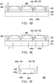
- FIG. 1 and FIG. 2 are a three-dimensional view and a cross-sectional view of a light emitting diode (LED) device of a first embodiment of the invention, wherein FIG. 1 is a schematic cross-sectional view taken along a line A-A' of the three-dimensional view of FIG. 2 .
- a LED device 10 includes a LED chip 12, an encapsulant 14, and a ring-shape barrier 16 in this embodiment.
- the encapsulant 14 covers the LED chip 12, and the ring-shape barrier 16 surrounds the encapsulant 14 and the LED chip 12.
- the LED device 10 includes a substrate 18, and the LED chip 12, the encapsulant 14 are disposed on the substrate 18.
- the substrate 18 is to be disposed is not limited by the invention, and the LED device may be a LED device without a substrate as described as follows.
- the ring-shape barrier 16 is disposed on the substrate 18, and a height of the ring-shape barrier 16 is equal to a height of the encapsulant 14. In this way, the ring-shape barrier 16 surrounds the LED chip 12 and the encapsulant 14 disposed on the substrate 18 and is adapted to reflect light rays emitted by the LED chip 12 and the encapsulant 14.
- the height of the ring-shape barrier 16 and the height of the encapsulant 14 are not limited to be equal in this embodiment, and the height of the ring-shape barrier 16 and the height of the encapsulant 14 may be unequal, which is described in detail as follows.
- the LED chip 12 may be selected from a horizontal chip, a vertical chip, or a flip chip.
- the LED chip 12 is preferably selected from a flip chip since a flip chip is not required to be electrically connected to the substrate through a metal wire, which is advantageous for miniaturization.
- methods such as direct bonding, eutectic bonding, golden ball or bump bonding, silver paste or solder paste bonding, etc. may be adopted to perform die bonding so as to be electrically connected to the substrate.
- the LED chip 12 includes a first surface 12a and a plurality of side surfaces 12b connected to the first surface 12a.
- the LED chip 12 has a plurality electrodes that are not shown, and each of the electrodes has an electrode terminal configured to be electrically connected to a conductive circuit pattern of the substrate or an external circuit.
- the substrate 18 also includes a top surface 18a and a plurality of external side surfaces 18b connected to the top surface 18a and thus is approximately be flat plate-shaped.
- the substrate 18 may be selected from a ceramic substrate, a plastic substrate, a printed circuit board (PCB), or a metal substrate.
- the substrate 18 selected from a ceramic substrate, a plastic substrate, or a PCB also includes the conductive circuit pattern that is not shown, such as a connection circuit or a plurality of contact points.
- the LED chip 12 is disposed on the top surface 18a of the substrate 18 and is connected to the contact points through the electrode terminals to be electrically connected to the substrate 18. Nevertheless, the invention does not limit the type of the substrate 18 nor a connection method in which the LED chip 12 is connected thereto.
- the encapsulant 14 covers the first surface 12a and the side surfaces 12b of the LED chip 12 and is located on the top surface 18a of the substrate 18 in this embodiment. Moreover, the encapsulant 14 is located between the side surfaces of the LED chip 120 and the ring-shape barrier 16, so that the LED chip 12 is not directly in contact with the ring-shape barrier 16.
- the encapsulant 14 may be any solid including a plane (i.e., a non-curved lens), for example, a cuboid, a cube, a trapezoidal prism, etc. for instance, a cuboid is taken as an example in FIG. 1 and FIG. 2 with a thickness of approximately 0.3 millimeters.
- the encapsulant 14 includes a second surface 14a and a plurality of side surfaces 14b connected to the side surface 14a.
- the second surface 14a of the encapsulant 14 is disposed on the first surface 12a of the LED chip 12, and the second surface 14a is substantially parallel to the first surface 12a.
- the side surfaces 14b of the encapsulant 14 are correspondingly disposed on the side surfaces 12b of the LED chip 12 to cover the first surface 12a and the side surfaces 12b of the LED chip 12. That is, the encapsulant 14 covers all external surfaces of the LED chip 12 except for a bottom surface of the LED chip 12 facing the substrate 18.
- a width t of the encapsulant 14 is provided between the side surface 12b of the LED chip 12 and the ring-shape barrier 16.
- the width t is preferably to be 0.05 to 0.4 times greater than a width of the chip, and more preferably 0.05 to 0.1 times greater corresponding to light shape improvement of the ring-shape barrier 16.
- the encapsulant 14 is a colloid with light transmittancy, and the material thereof is selected from one of the following groups: a silicone resin composition, an epoxy resin composition, and a combination of the foregoing.
- a method of forming the encapsulant 14 may include a screen printing process, a molding process, a lamination process, a coating process, or other suitable processes. Taking the lamination process for example, a pre-formed semi-cured prepreg (e.g., a prepreg cured to the B-stage) is stacked on the substrate 18 and the LED chip 12 and then is heated and/or baked. In this way, the encapsulant is formed not through injecting plastic into a mold as in the molding process, so that uneven injection of plastic is avoided.
- the plastic is prevented from unexpectedly flowing to and between an electrode of the flip chip and a carrier when the lamination process is adopted, which may affect electrical connection capability of the flip chip.
- a fluorescence material may be included in the encapsulant 14 to absorb and convert part of the light emitted by the LED chip 12 into light of other colors and simultaneously mix the absorbed light with the converted light to produce light of other colors, such as white light.
- the fluorescence material may be selected from one of or a plurality of the following groups: Sr 5 (PO 4 ) 3 Cl:Eu 2+ , (Sr,Ba)MgAl 10 O 17 :Eu 2+ , (Sr,Ba) 3 MgSi 2 O 8 :Eu 2+ , SrAl 2 O 4 :Eu 2+ , SrBaSiO 4 :Eu 2+ , CdS:In, CaS:Ce 3+ , Y 3 (Al,Gd) 5 O 12 :Ce 2+ , Ca 3 Sc 2 Si 3 O 12 :Ce 3+ , SrSiON:Eu 2+ , ZnS:Al 3+ ,Cu + , CaS:Sn 2+ , CaS:Sn 2+ ,F, CaSO 4 :Ce 3+ ,Mn 2+ , LiAlO 2 :Mn 2+ , BaMgAl 10 O 17 :Eu
- a juncture 14c of the second surface 14a and each of the side surfaces 14b of the encapsulant 14 is formed at a right angle.
- the second surface 14a is shown a flat surface. Nevertheless, in other variations provided by other embodiments that are not shown, the second surface of the encapsulant may be processed to be a rough surface through a roughening process, so as to reduce internal total reflection and increase a proportion of light refraction to change a light output effect.
- the third surface 16a of the ring-shape barrier 16 may also be designed to be a rough surface, and a degree of roughness of the third surface 16a may be similar to that of the second surface 14a. Nevertheless, the invention is not limited thereto. Those having ordinary skill in the art may change the degrees of roughness of the second surface 14a and the third surface 16a according to application requirements.
- the ring-shape barrier 16 surrounds the encapsulant 14 and the LED chip 12 and is located on the top surface 18a of the substrate 18.
- the ring-shape barrier 16 is adapted to reflect a light ray emitted by the LED chip 12 and converted through the fluorescence material in the encapsulant 14.
- a material of the ring-shape barrier 16 is a resin composition containing reflective particles.
- the resin composition may be selected from one of the following groups: a silicone resin composition, an epoxy resin composition, and a combination of the foregoing.
- the reflective particles may be selected from one of the following groups: TiO 2 , SiO 2 , ZnO, ZrO 2 , BN, BaSiO 4 , MgO, and a combination of the foregoing.
- a reflection rate of the light emitted by the LED chip 12 and converted/mixed through the encapsulant and reflected by the ring-shape barrier 16 is greater than 80%, and preferably greater than 95%.
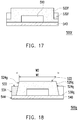
- structural design of the ring-shape barrier 16 may also affect the light output effect (e.g., a light output angle) of the LED device 10.
- a width of a barrier may slightly affect light-blocking capability of the barrier, so that the barrier is preferably to be formed of a uniform width so as to provide uniform light-blocking capability.
- the ring-shape barrier 16 of a uniform width is shown to surround the encapsulant 14.
- the width of the barrier is approximately 0.1 millimeters but is not limited thereto.
- the ring-shape barrier may be formed of an un-uniform width corresponding to different end product needs.
- the ring-shape barrier 16 includes the third surface 16a and a plurality of external side surfaces 16b connected to the third surface 16a.
- the third surface 16a of the ring-shape barrier 16 surrounds the side surfaces 14b of the encapsulant 14, and the external side surfaces 16b of the ring-shape barrier 16 correspond to the side surfaces 12b of the LED chip 12 and the side surfaces 14b of the encapsulant 14.
- a juncture 16c of the third surface 16a and each of the external side surfaces 16b of the ring-shape barrier 16 is formed at a right angle.
- the third surface 16a may be a convex surface, a concave surface, or an inclined surface.
- the external side surfaces 16b of the ring-shape barrier 16 may further be flushed with the external side surfaces 18b of the substrate 18, but the invention is not limited thereto.
- the external side surface 16b of the ring-shape barrier 16 may not be flushed with the external side surfaces 18b of the substrate 18.
- a method of manufacturing the LED device of this embodiment is described in detail with reference to FIG. 3A to FIG. 3G .
- FIG. 3A to FIG. 3G are flowcharts of a method of manufacturing the LED device of the first embodiment of the invention.
- a carrier 110 as shown in FIG. 3A to be formed into a substrate in a following singulation step is provided, and thus, a material of the carrier 110 is selected to be identical to that of the substrate.
- a plurality of LED chips 130 are disposed on the carrier 110 as shown in FIG. 3B .
- An electrode terminal 132a of each of the LED chips 130 is electrically connected to a conductive circuit pattern (not shown) on the carrier.
- Three flip chips 130 are schematically illustrated in FIG. 3B and are electrically to the conductive circuit patterns on the carrier through a direct bonding method.
- the invention is not intended to limit a number of the LED chips 130. Practically, the number of the LED chips 130 may be greater, and the LED chips 130 may be arranged on the carrier in numeric groups.
- a gap is required to be appropriately calculated and adjusted so as to achieve chip scale packaging after cutting.
- the gap between the LED chips 130 is preferably equal to or less than 0.8 times a width of the chip, and is preferable equal to or less than 0.7 times the width of the chip.
- an encapsulant 140 is formed on the carrier 110, wherein the encapsulant 140 covers the LED chips 130.
- the material selected for and the method of forming the encapsulant 140 are described above.
- the encapsulant 140 is then pre-cut through a cutting tool 50 to form a patterned trench 140a in the encapsulant 140, wherein each of the LED chips 130 is surrounded by the patterned trench 140a.
- the encapsulant 140 in a step of cutting the encapsulant 140, is cut in a direction perpendicular to the carrier 110, and that a side surface (i.e., an inner wall of the patterned trench 140a) of the cut encapsulant 140 becomes a plane and is further perpendicular to the carrier 110.
- a surface of the carrier 110 may be exposed by the patterned trench 140a, or the surface of the carrier may not be exposed by the patterned trench 140a and thus only a concave structure which is concave towards the carrier 110 is formed. People having ordinary skill in the art may select a depth of the patterned trench according to application features of the end products with reference to the content of the invention.
- a reflection colloid 150 is formed in the patterned trench 140a, as such, the reflection colloid 150 is distributed between the LED chips 130, wherein a height of the reflection colloid 150 is proximately identical to that of the encapsulant 140.
- a material selected for the reflection colloid 150 is identical to the material selected for the ring-shape barrier.
- the reflection colloid 150 is cut through a cutting tool 60 to perform singulation to the encapsulant 140 and the LED chips 130 to form a plurality of LED devices 100.
- a material of the cutting tools 50/60 is selected from one of the following groups: diamond, mental, resin, and a combination of the foregoing.
- a laser beam may also be used to replace the cutting tool 50/60 for cutting; nevertheless, the cutting tool 50/60 is still preferably used for cutting because undesirable coke contaminant is less likely to be produced.
- the LED devices 100 of this invention are formed after the steps shown in FIG. 3A to FIG. 3G .
- a quality test may be performed to each of the LED devices 100 to determine whether each of the LED chips 100 achieves the expected light output effect.
- the foregoing embodiment describes LED devices having a substrate; nevertheless, a form without a substrate may also be included in the invention.
- the second embodiment describes a LED device of the invention without a substrate as follows.
- FIG. 4 is a schematic cross-sectional view of a LED device of the second embodiment of the invention.
- a LED device 200 includes a LED chip 230, an encapsulant 240, and a ring-shape barrier 250'.
- the encapsulant 240 covers the LED chip 230
- the ring-shape barrier 250' surrounds the encapsulant 240 and the LED chip 230.
- a height of the ring-shape barrier 250' and a height of the encapsulant 240 are equal, as such, the ring-shape barrier 250' is adapted to reflect light rays emitted by the LED chip 230 and the encapsulant 240.
- the height of the ring-shape barrier 250' and the height of the encapsulant 240 are not limited to be equal in this embodiment, and the height of the ring-shape barrier 250' and the height of the encapsulant 240 may be unequal, which is described in detail as follows.
- the LED device is in a form without a substrate, an electrode terminal 232a of the LED chip 230 is required to be exposed outside the encapsulant 240 to be electrically connected to an external circuit in the second embodiment.
- the LED chip is preferably a flip chip.
- a bottom surface of the LED chip may be exposed outside the encapsulant.
- the invention is not limited thereto, and only the electrode terminal is exposed outside the encapsulant, and the bottom surface of the LED chip is encapsulated in the encapsulant.
- the LED chip 230 in FIG. 4 is a flip chip and has a top surface 230a, at least one side surface 230b, and a bottom surface 230c opposite to the top surface 230a.
- the LED chip 230 has a plurality of electrodes 232, and each of the electrodes 232 has an electrode terminal 232a.
- the encapsulant 240 covers the top surface 230a of the LED chip 230 but exposes the bottom surface 230c and the electrode terminals 232a.
- the ring-shape barrier 250' is connected to the encapsulant 240 and is aligned to the side surface 230b of the LED chip 230.
- the LED device 200 is a packaging form without a substrate
- the electrodes 232 and a bottom surface 240c of the encapsulant 240 are substantially coplanar (i.e., the electrode terminals 232a and the bottom surface 240c are coplanar).
- the electrodes 232 are preferably to have a considerable thickness, so that the electrode terminals 232a protrude outwards from the bottom surface 240c of the encapsulant 240. In this way, heat dissipation effect is enhanced, and a soldering area in following applications is simultaneously increased, and that a soldering strength is further enhanced. Nevertheless, an excessive step height may lead to light leakage at the bottom surface 230c.
- the step height is preferably between 3 ⁇ m and 20 ⁇ m, more preferably between 5 ⁇ m and 10 ⁇ m.
- the electrodes are preferably to cover 50% or greater of an area of the chip bottom surface 230c.
- areas of the two positive and negative electrodes are preferably to be designed to be equal.
- a reflection layer may be selectively designed to be included in the flip chip. An area of the reflection layer is required to exceed 50% of the area of the bottom surface, and preferably covers 80% of the area of the bottom surface, so as to solve the light leakage problem which is likely to occur at the chip bottom surface 230c.
- the area of the encapsulant bottom surface 240c is expected to be lowered as much as possible, so as to prevent the possible light leakage problem from occurring.
- the area of the encapsulant bottom surface 240c is preferably to be 20% or less of an area of a light output surface 240b, more preferably 10% or less.
- a shape of the ring-shape barrier may be additionally designed.
- the area of the bottom surface 250c of the ring-shape barrier is increased, and that the bottom surface 250c of the ring-shape barrier is greater than the bottom surface 240c of the encapsulant.
- the possibility of light leakage at the bottom surface may also be reduced, and related design of the ring-shape barrier is described through variations provided by other embodiments.
- a method of manufacturing the LED device of this embodiment is described in detail with reference to FIG. 5A to FIG. 5G .
- a light transmissive carrier 210 is provided, and a soluble adhesive layer 220 is formed on the light transmissive carrier 210 through spray coating, brush coating, and soaking, or other suitable methods.
- the light transmissive carrier 210 may be a glass carrier or a plastic carrier.
- the soluble adhesive layer 220 may be a photolysis or pyrolysis sticky material, preferably the photolysis sticky material, for example, an ultraviolet light release tape.
- a plurality of LED chips 230 are disposed on the soluble adhesive layer 220, and an electrode terminal 232a of each of the LED chips 230 faces the soluble adhesive layer 220.
- an encapsulant 240 is then formed on the soluble adhesive layer 220, wherein the encapsulant 240 covers the LED chips 230, and the encapsulant 240 does not cover the electrode terminals 232a of electrodes 232.
- the encapsulant 240 is then pre-cut through a cutting tool 50 to form a patterned trench 240a in the encapsulant 240, wherein each of the LED chips 230 is surrounded by the patterned trench 240a.
- a reflection colloid 250 is then formed in the patterned trench 240a, as such, the reflection colloid 250 is distributed between the LED chips 230.
- the reflection colloid 250 is then cut through a cutting tool 60 to perform singulation to the encapsulant 240 and the LED chips 230 to form a plurality of LED devices 200.
- a light ray L is provided, wherein the light ray L is, for example, an ultraviolet light and irradiates the soluble adhesive layer 220 through the light transmissive carrier 210, so as to reduce adhesiveness of the soluble adhesive layer 220.
- each of the LED devices 200 can be separated from the soluble adhesive layer 220 and the light transmissive carrier 210 so as to be in a state shown in FIG. 4 . Accordingly, the LED devices are manufactured without a substrate. After being separated, the electrode terminals 232a of the LED chips 230 are exposed outside the encapsulant 240. In addition, as described above, a quality test may be performed to each of the LED devices 200 to determine whether each of the LED chips 200 achieves the expected light output effect.
- a side surface of the ring-shape barrier may be inclined with respect to a side surface of the LED chip to further increase light output efficiency.
- the variation examples are described in detailed with reference to FIG. 5A to FIG. 5C and FIG. 6A to FIG. 6F .
- a difference between a LED device 400 of this variation example and the LED device 200 includes that an encapsulant 440 is shaped as an inverted trapezoid, and a reflection surface 450a of a ring-shape barrier 450' is inclined with respect to a side surface 430b of a LED chip 430. That is, a distance between the reflection surface 450a and the side surface 430b gradually decreases in a direction away from a light output surface 440b. Accordingly, the reflection surface 450a can more effectively reflect light rays towards the light output surface 440b, so as to further increase light output efficiency of the LED device 400.
- the reflection surface 450a is a plane type inclined wall.
- the reflection surface may be a curved-surface wall of a concave surface type, a convex surface type, or a surface of a suitable type in other embodiments.
- the shape of the reflection surface may be designed and formed through adopting different types of a cutting tool 50'.
- a method of manufacturing the LED device of this embodiment is described in detail with reference to FIG. 5A to FIG. 5C and FIG. 6A to FIG. 6F .
- the encapsulant 440 and the LED chips 430 are flipped over and are adhered onto another carrier 410' having a soluble adhesive layer 420' as shown in FIG. 6A .
- the carrier 410' is then de-bonded and separated, and that a bottom surface 430c of each of the LED chips 430 faces upwards.
- the encapsulant 440 is then pre-cut through a cutting tool 50' to form a patterned trench 440a in the encapsulant 440, wherein each of the LED chips 430 is surrounded by the patterned trench 440a.
- the cutting tool 50' of this variation example has an inclined surface 50a.
- the surface 50a of the cutting tool 50' is inclined with respect to a side surface 430b of each of the LED chips 430 and corresponds to an inner wall of the patterned trench 440a. Accordingly, the inner wall of the patterned trench 440a is inclined with respect to the side surface 430b of each of the LED chips 430 as shown in FIG. 6B .
- a reflection colloid 450 is then formed in the patterned trench 440a, as such, the reflection colloid 450 is distributed between the LED chips 430.
- a cross-section of the reflection colloid 450 is shaped as a letter V as shown in FIG. 6C .
- a cross-section of the ring-shape barrier may also be shaped as a letter U.
- the reflection colloid 450 is then cut through a cutting tool 60" to perform singulation to the encapsulant 440 and the flip chips 430 to form a plurality of LED devices 400.
- a light ray L" is provided, and the light ray L" irradiates the soluble adhesive layer 420', so as to reduce adhesiveness of the soluble adhesive layer 420'.
- each of the LED devices 400 can be separated from the soluble adhesive layer 420' and the light transmissive carrier 410' so as to be in a state shown in FIG. 6F .
- a quality test may be performed to each of the LED devices 400 after de-bonding to determine whether each of the LED chips 400 achieves the expected light output effect.
- the encapsulant may be entirely disposed on the LED chips and the ring-shape barrier, and moreover, the ring-shape barrier is in contact with the LED chips directly.
- the variation example is described in detail with reference to FIG. 5A to FIG. 5B and FIG. 7A to FIG. 7E .
- a difference between a LED device 300 of this variation example and the LED device 100 includes that an encapsulant 340 does not extend between a side surface 330b of a LED chip 330 and a ring-shape barrier 350', and the ring-shape barrier 350' directly covers the side surface 330b of the LED 330. Accordingly, a light ray emitted by the LED chip 330 is more concentrated to be emitted from a light output surface 340b to increase light output efficiency, and a quantity of the encapsulant 340 to be used can be reduced to save material costs.
- a top surface 350b of the ring-shape barrier 350' in this variable example is coplanar with a top surface 330a of the LED chip 330.
- a method of manufacturing the LED device of this embodiment is described in detail with reference to FIG. 5A to FIG. 5B and FIG. 7A to FIG. 7E .
- a reflection colloid 350 is formed on a soluble adhesive layer 320 as shown in FIG. 7A , wherein the reflection colloid 350 fills gaps between the LED chips 330.
- an encapsulant 340 is then formed on the LED chips 330 and the reflection colloid 350, wherein the encapsulant 340 covers the LED chips 330, and the encapsulant 340 does not cover electrode terminals 332a of LED chips 330.
- the encapsulant 340 and the reflection colloid 350 are then cut through a cutting tool 60' to perform singulation to the encapsulant 340 and the LED chips 330 to form a plurality of LED devices 300.
- a light ray L' is provided to reduce adhesiveness of the soluble adhesive layer 320.
- each of the LED devices 300 can be separated from the soluble adhesive layer 320 and the light transmissive carrier 310 so as to be in a state shown in FIG. 7E .
- a quality test may be performed to each of the LED devices 300 after de-bonding to determine whether each of the LED chips 300 achieves the expected light output effect.
- the height of the ring-shape barrier and the height of the encapsulant are equal. Nevertheless, a LED device in which a height of a ring-shape barrier and a height of an encapsulant are unequal is also provided in the invention so as to further adjust the light output angle.
- a third embodiment is provided to give detailed description.
- FIG. 8 and FIG. 9 are a three-dimensional view and a cross-sectional view of a LED device of the third embodiment of the invention, wherein FIG. 8 is a schematic cross-sectional view taken along a line B-B' of the three-dimensional view of FIG. 9 .
- a LED chip 510 has a first surface 512
- an encapsulant 520 has a second surface, 522
- a ring-shape barrier 530 has a third surface 532.
- the second surface 522 is higher than the third surface 532.
- the first surface 512 and the second surface 522 define a first height H1, and the first surface 512 and the third surface 532 define a second height H2.
- first surface, the second surface, and the third surface are inclined surfaces
- vertical heights of highest points (i.e., end points) after the first surface, the second surface, and the third surface are projected are defined as the first height H1 and the second height H2.
- surfaces of the components are plane surfaces, any point on the plane surface is the "end point", and the height is a vertical distance between two end points.
- any point on the first surface 512 of the LED chip 510 can be defined as a first end point PI
- any point on the second surface 522 of the encapsulant 520 can be defined as a second end point P2
- any point on the third surface 532 of the ring-shape barrier 530 can be defined as a third end-point P3.
- the first height H1 may be defined by the first end point P1 of the first surface 512 and the second end point P2 of the second surface 522
- the second height H2 may be defined by the first end point P1 of the first surface 512 and the third end-point P3 of the third surface 532. Accordingly, since the second surface 522 of this embodiment is higher than the third surface 532, the first height H1 is greater than the second height H2. That is, the third end-point P3 is closer to the first end point P1 than the second end point P2 based on the first end point P1.
- a height of the ring-shape barrier 530 (taking the third end-point P3 on the third surface 532 as the highest point) is lower than a height of the encapsulant 520 (taking the second end point P2 on the second surface 522 as the highest point).
- the concept of changing the ring-shape barrier in the third embodiment may be applied to the LED device with a substrate and the LED device without a substrate, that is, the third embodiment may be combined with the first embodiment or the second embodiment.
- Forms in which a substrate is present or not present is to be described as follows.
- the degrees of roughness of the encapsulant and the ring-shape barrier may be adjusted to change the light output efficiency.
- a degree of roughness of a fourth surface 552 i.e., a side surface of the encapsulant 520 exposed outside the ring-shape barrier 530
- the second surface 522 may be similar to a flat surface
- the fourth surface 552 may be a rough surface, and that the degree of roughness of the fourth surface 552 is greater than that of the second surface 522.
- the third surface 532 of the ring-shape barrier 530 may also be designed to be a rough surface, and a degree of roughness of the third surface 532 may be similar to that of the fourth surface 552.
- an area of the third surface 532 may be increased. Since the entire area of the third surface 532 is greater than an entire area of the fourth surface 552. Nevertheless, the invention is not limited thereto. Those having ordinary skill in the art may change a proportion of the third surface 532 to the fourth surface 552 according to application requirements.
- a method of manufacturing the LED device of the third embodiment is described in detail with reference to FIG. 3A to FIG. 3D and FIG. 10A to FIG. 10B .
- a portion of a reflection colloid 506 is removed as shown in FIG. 10A , such that a top surface 506a of the reflection colloid 506 is lower than the second surface 522 of the encapsulant 520. That is, the reflection colloid 506 which is as high as the encapsulant 520 in FIG. 3D is lower than the encapsulant 520 in this step.
- a method of removing a portion of the reflection colloid 506 includes removing a portion of the reflection colloid 506 in a direction parallel to a carrier 502. In this case, the top surface 506a of the reflection colloid 506 is a plane and is parallel to the carrier 502.
- a height of the reflection colloid 506 relative to the carrier 502 may be greater than the height of the LED chip 510 relative to the carrier 502. That is, the reflection colloid 506 is lower than the encapsulant 520 but is higher than the LED chip 510.
- the reflection colloid 506 is then cut along a trench 504 so that the reflection colloid 506 becomes a plurality of the ring-shape barriers 530, that is, the singulation step described above.
- the ring-shape barriers 530 correspondingly surround the LED chip 510 and the encapsulant 520.
- Each of the ring-shape barriers 530 has the third surface 532 to define the third end-point P3.
- the first surface 512 and the corresponding third surface 532 define the second height H2, wherein the first height H1 is greater than the second height H2.
- the form shown in FIG. 10 is a LED device with a substrate. When singulation is performed, the carrier 502 is required to be simultaneously or subsequently cut to form the LED device 500 with a substrate 540.
- the LED device 500 may be formed right after an adhesive layer 506 is cut.
- the carrier 502 may be selectively cut or may not be selectively cut, and the LED device 500 and the carrier 502 are separated subsequently (i.e., forming the LED device 500 without a substrate).
- a light transmissive carrier similar to the light transmissive carrier 210 having the soluble adhesive layer 220 as shown in FIG. 5A may be provided.
- a light ray L may be provided to irradiate a soluble adhesive layer 620 to reduce adhesiveness of the soluble adhesive layer 620 as shown in FIG. 11A .
- each of the LED devices 600 can be separated from the soluble adhesive layer 620 and a light transmissive carrier 610 so as to be in a state shown in FIG. 11B .
- a quality test may be performed to each of the LED devices 600 after de-bonding to determine whether each of the LED chips 600 achieves the expected light output effect.
- FIG. 12 and FIG. 13 are graphs of light output intensity of the LED device of FIG. 9 and other LED devices at each angle on an X axis and a Y axis in a space coordinate system.
- the ring-shape barrier 530 is adapted to reflect light rays emitted by the LED chip 510 and the encapsulant 520 in this embodiment. That is, structural design of the ring-shape barrier 530 affects light output effect (e.g., light output angle) of the LED device 500.
- the "light output angle” refers to an angle range of a ratio greater than 0.5 of a light output volume of the LED device 500 at each angle on a plane (i.e., the viewing angle shown in FIG. 9 ) constituted by a Z axis (i.e., an axis direction perpendicular to a light emission surface of the LED chip 510) on which the LED device 500 is located and a single axis direction on an XY plane (i.e., the X axis or the Y axis) to the light output volume of the LED device 500 at 0 degree (i.e., a Z axis direction) when the LED device 500 is placed in a space coordinate system XYZ.
- a Z axis i.e., an axis direction perpendicular to a light emission surface of the LED chip 510
- XY plane i.e., the X axis or the Y axis
- a ratio of the light output volumes of the LED device 500 (the height of the ring-shape barrier 530 is half of the height of the encapsulant 520, as shown in FIG. 9 ) at +65 degrees and - 65 degrees (i.e., the curve 1) to the light output volume of the LED device 500 at 0 degree (i.e., the Z axis direction) is 0.5.
- the light output angle of the LED device 500 is 530 degrees (covering +65 degrees and -65 degrees).
- a ratio of light output volumes of the LED device of the first embodiment at +60 degrees and -60 degrees (i.e., the curve 3) to the light output volume of the LED device of the first embodiment at 0 degree (i.e., the Z axis direction) is 0.5.
- the light output angle of the LED device of the first embodiment is 120 degrees (covering +60 degrees and -60 degrees).
- an emission angle of the LED device is further expanded (approximately 140 degrees) if the ring-shape barrier is omitted (i.e., the curve 2), the light rays can not be concentrated through reflection, and that light output brightness and light output uniformity are considerably lowered.
- the LED device 100 of the third embodiment has a greater emission angle on an axis direction X compared to the LED device of the first embodiment (the curve 3); nevertheless, the effect of light ray concentration through reflection originally provided by the ring-shape barrier 530 is maintained.
- taking light output intensity of the LED device 100 at each angle on the Y axis in the space coordinate system i.e., FIG.
- the LED device 500 of the third embodiment has a greater emission angle on an axis direction Y compared to the existing LED device (the curve 3), and moreover, the effect of light ray concentration through reflection originally provided by the ring-shape barrier 530 is maintained.
- the effect of changing the light output angle is provided in the LED device of the third embodiment compared to that of the first embodiment.
- the light output angle is required to be slightly expanded owing to market demand
- people having ordinary skill in the art may change the structure of the LED device 500 with reference to the invention and do not have to re-design the lenses to satisfy the demand. It thus can be seen that the LED device 500 provided by the invention features favorable industrial applications.
- FIG. 14 to FIG. 25 are schematic cross-sectional views of a LED device of other variation examples of this embodiment.
- a LED device 500a includes a LED chip 510a, the encapsulant 520, the ring-shape barrier 530, and a substrate 540a.
- a structure of the LED device 500a is similar to that of the LED device 500, and a difference therebetween includes that the LED chip 510 shown in FIG. 9 is a flip chip electrically connected to a circuit pattern (not shown) on the substrate 540 through a flip-chip bonding process, but the LED chip 510a of this variation example is a horizontal chip.
- An electrode of the LED chip 510a is located at an upper side of the LED chip 510a and is required to be connected to an circuit pattern 546 on the substrate 540a through a plurality of wires 516 after the LED chip 510a is disposed on the substrate 540a. Accordingly, when the LED device 500a is manufactured through the foregoing manufacturing method, the step in which the LED chip 510a is disposed on the substrate 540a acting as the carrier 502 (shown in FIG. 10A ) includes a wire bonding process, that is, the LED chip 510a is electrically connected to the substrate 540a through the wires 516. It thus can be seen that the type of the LED chip and the specific technical method in which the LED chip is electrically connected to the substrate are not limited by the invention and may be adjusted as required.
- a LED device 500b includes the LED chip 510, the encapsulant 520, the ring-shape barrier 530, and a substrate 540b.
- a structure of the LED device 500b is similar to that of the LED device 500, and a difference therebetween includes that the substrate 540 is a one-piece substrate, such as a ceramic substrate, a plastic substrate, or a printed circuit substrate, but the substrate 540b of this variation example is a metal substrate and is a separated substrate.
- the LED chip 510 is electrically connected to the substrate 540b through the electrode of the LED chip 510, and portions of the substrate 540b being connected to the electrode are separated from each other so as to avoid occurrence of a short circuit.
- the LED device 500b may also be manufactured through the foregoing manufacturing method. Accordingly, the type of the substrate is not limited by the invention and may be adjusted as required. In addition, gaps in the substrate 540 may be filled with or may not be filled with the encapsulant 520 corresponding to process differences.
- a LED device 500c includes the LED chip 510, the encapsulant 520, a ring-shape barrier 530c, and a substrate 540c.
- a structure of the LED device 500c is similar to that of the LED device 500, and a difference therebetween is that the ring-shape barrier 530 surrounds the encapsulant 520 and the LED chip 510 and is located on the top surface 542 of the substrate 540, but the ring-shape barrier 530c of this variation example surrounds the encapsulant 520 and the LED chip 510 and further surrounds the substrate 540c.
- the ring-shape barrier 530c is located outside the LED chip 510, the encapsulant 520, and the substrate 540c and is located on an outer surface 544 of the substrate 540c. Therefore, when the LED device 500c is manufactured through the foregoing manufacturing method, the carrier 502 may be simultaneously or subsequently cut during the step in which the encapsulant is cut, as such, the patterned trench 504 extends into the carrier 502. The steps of forming the reflection colloid 506, removing a portion of the reflection colloid 506, and cutting the reflection colloid 506 as shown in FIG. 10A to FIG. 10B and are performed subsequently. Finally, the ring-shape barrier 530c surrounds the outer surface 544 of the substrate 540c.
- the trench 504 extends into the entire carrier 502 as shown in FIG. 16 .
- the carrier 502 is not limited to be entirely cut, and it may be that only a portion of the carrier 502 is cut. That is, the ring-shape barrier 530c may extend into only a portion of the carrier 502 (or a side wall of the substrate 540) and do not penetrate the carrier 502. It thus can be seen that a positional relation between the ring-shape barrier and the substrate is not limited by the invention and may be adjusted as required.
- a LED device 500f includes the LED chip 510, an encapsulant 520f, a ring-shape barrier 530f, and the substrate 540.
- a structure of the LED device 500f is similar to that of the LED device 500, and a difference therebetween includes that the ring-shape barrier 530 is disposed on the top surface 542 of the substrate 540 and is in contact with the substrate 540, but the ring-shape barrier 530f of this variation example is located above a portion of the encapsulant 520.
- the ring-shape barrier 530f is not in contact with the substrate 540, and a portion of the encapsulant 520 extends between the ring-shape barrier 530f and the substrate 540. Therefore, when the LED device 500f is manufactured through the foregoing manufacturing method, in the step of cutting the encapsulant 520f and forming the patterned trench 504, the cut encapsulant 520f is not exposed outside the surface of the substrate 540.
- the reflection colloid 506 filling the patterned trench 504 subsequently constitutes the ring-shape barrier 530f and is located above a portion of the encapsulant 520f. It thus can be seen that a relation position between the ring-shape barrier and the substrate is not limited by the invention and may be adjusted as required.
- a LED device 500g includes the LED chip 510, an encapsulant 520g, a ring-shape barrier 530g, and the substrate 540.
- a structure of the LED device 500g is similar to that of the LED device 500, and a difference therebetween includes that each side surface 524 of the encapsulant 520 is perpendicular to the substrate 540 and that the encapsulant 520 has a uniform thickness in a vertical direction, but each side surface 524g of the encapsulant 520g of this variation example is an inclined surface.
- a height of the side surface 524g decreases from one end adjacent to the LED chip 510 towards the other end away from the LED chip 510, and that a width of the encapsulant 520g increases towards the substrate 540 (or the carrier).
- a width W1 of a second surface 522 of the encapsulant 520g is less than a width W2 of a bottom surface of the encapsulant 520g in contact with the substrate 540, and that a cross-section of the encapsulant 520g is shaped as a trapezoid.
- a cutting tool with an inclined surface is used to cut the encapsulant 520g, and that the side surface 524g of the encapsulant 520g is shaped as an inclined surface as well.
- an external side surface 534 of the ring-shape barrier 530g may be maintained to be a plane with reference to the embodiment of FIG. 9 and is flushed with an external side surface 544 of the substrate 540.
- a width of the ring-shape barrier 530g decreases towards the substrate 540 (or the carrier), and that a cross-section of the ring-shape barrier 530g is shaped as a trapezoid or a triangle.
- the adhesive layer 506 configured for forming the ring-shape barrier 530g fills into the trench 504 and covers the side surface 524g shaped as an inclined surface on the encapsulant 520g.
- the adhesive layer 506 is then cut in the vertical direction in the step of FIG. 10B , as such, the external side surface 534 of the ring-shape barrier 530g is shaped as a plane and is flushed with the side surface 544 of the substrate 540.
- a LED device 500h features the design identical to that of the encapsulant 520g; nevertheless, each external side surface 534h of a ring-shape barrier 530h of the LED device 500h is an inclined surface.
- the external side surface 534h refers to the side surface on the ring-shape barrier 530h which is not in contact with the encapsulant 520.
- a height of the external side surface 534h decreases from one end adjacent to the LED chip 510 towards the other end away from the LED chip 510, and that a cross-section of the ring-shape barrier 530h is shaped as a trapezoid or a triangle and may also be shaped as a parallelogram (i.e., the external side surface 534h is parallel to the side surface 524g). Therefore, when the LED device 500h is manufactured through the foregoing manufacturing method, the adhesive layer 506 configured for forming the ring-shape barrier 530h fills into the trench 504 and covers the side surface 524g shaped as an inclined surface on the encapsulant 520g. In the step of FIG.
- the adhesive layer 506 is then cut in a direction inclined with respect to the carrier 502/the substrate 540 rather than in the vertical direction by a cutting tool with an inclined surface, as such, the external side surface 534h of the ring-shape barrier 530h is shaped as an inclined surface.
- a LED device 500i includes the LED chip 510, the encapsulant 520, a ring-shape barrier 530i, and the substrate 540.
- a structure of the LED device 500i is similar to that of the LED device 500, and a difference therebetween includes that the third surface 532 of the ring-shape barrier 530 is a plane, but a third surface 532i of the ring-shape barrier 530i of this variation example is shaped as an inclined surface. As such, a height of the third surface 532i decreases from one end adjacent to the LED chip 510 towards the other end away from the LED chip 510.
- one end of the third surface 532i in contact with the encapsulant 520 is higher than the other end of the third surface 532i in contact with an external side surface 534. Therefore, when the LED device 500i is manufactured through the foregoing manufacturing method, in the step of removing a portion of the adhesive layer 506 (i.e., the step of FIG. 10A ), the portion of the adhesive layer 506 is also removed in a direction inclined with respect to the carrier 502/the substrate 540, as such, the third surface 532i of the ring-shape barrier 530i is shaped as an inclined surface.
- a third end-point P3 of the ring-shape barrier 530i is located at a highest point of the third surface 532i, and that the second height H2 is defined by the third point P3 under such circumstances.
- the shapes of the encapsulant and the ring-shape barrier are not limited by the invention based on the embodiment of FIG. 18 to FIG. 20 and may be adjusted as required.
- a LED device 500j includes the LED chip 510, an encapsulant 520j, the ring-shape barrier 530, and the substrate 540.
- a structure of the LED device 500i is similar to that of the LED device 500, and a difference therebetween includes that the juncture C1 of the second surface 522 of the encapsulant 520 and each side surface 524 is formed at the right angle, but a step G1 is provided at a juncture C1 of a second surface 522 of the encapsulant 520j and each side surface 524 of this variation example and that a stair-shaped structure is formed.
- the step G1 of the encapsulant 520j has a step surface 526 connected to the ring-shape barrier.
- the juncture C1 is recessed towards an inner portion of the encapsulant 520j.
- the second surface 522 is higher than the step surface 526 to form the step-shaped structure, and a second end point P2 of the encapsulant 520j is located on the second surface 522.
- the step surface 526 and a third surface 532 of the ring-shape barrier 530 may further form a continuous surface. That is, a height of the step surface 526 is equal to a height of the third surface 532. Nevertheless, the invention is not limited thereto, and the third surface 532 may be higher than or lower than the step surface 526. Therefore, when the LED device 500j is manufactured through the foregoing manufacturing method, in the step of removing a portion of the adhesive layer 506 (i.e., the step of FIG.
- a portion of the encapsulant 520j is also removed, and that a periphery of the encapsulant 520j (i.e., the juncture C1) is shaped as a step-shaped structure to constitute the step G1.
- the step surface 526 is as high as the third surface 532 of the ring-shape barrier 530.
- a LED device 500k includes the LED chip 510, the encapsulant 520, a ring-shape barrier 530k, and the substrate 540.
- a structure of the LED device 500k is similar to that of the LED device 500, and a difference therebetween includes that the ring-shape barrier 530k is not entirely cut and that a top surface 536 of the ring-shape barrier 530k is created.
- a thickness of the top surface 536 is relatively thin, and that light transmissive effect of a certain degree is provided.
- the top surface 356 is not the third surface.
- a step G2 is provided at a juncture C2 of the top surface 536 and each external side surface 534 of the ring-shape barrier 530k, and that a step-shaped structure is formed. Moreover, the step G2 has a step surface to constitute a third surface 532. That is, the step G2 of the ring-shape barrier 530k has the step surface connected to the corresponding external side surface 534, and the step surface is the third surface 532 under such circumstances.
- the juncture C2 is recessed towards an inner portion of the ring-shape barrier 530, as such, the top surface 536 is higher than the step surface (the third surface) to be shaped as the stair-shaped structure.
- the top surface 536 of the ring-shape barrier 530k and the second surface 522 of the encapsulant 520 may further form a continuous surface. That is, a height of the top surface 536 is equal to a height of the second surface 522. At this time, the third surface 532 is lower than the second surface 522 of the ring-shape barrier 530k. Nevertheless, the invention is not limited thereto, and adjustment may be made according to requirements. Therefore, when the LED device 500k is manufactured through the foregoing manufacturing method, in the step of removing a portion of the reflection colloid 506 (i.e., the step of FIG.
- a width of the portion of the reflection colloid 506 being removed is less than a half of a width of the trench 504 (shown in FIG. 10A ), preferably less than a quarter. That is, in the step of removing a portion of the reflection colloid 506, the side surface 524 of the encapsulant 520 is not exposed. As such, the top surface 536 of the ring-shape barrier 530k and the second surface 522 of the encapsulant 520 forms a continuous surface, and the step G2 shaped as a stair structure if formed at the juncture C2.
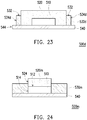
- a LED device 500d includes the LED chip 510, the encapsulant 520, a ring-shape barrier 530d, and a substrate 540.
- a structure of the LED device 500d is similar to that of the LED device 500, and a difference therebetween includes that the substrate 534 of the ring-shape barrier 530 is flushed with the external side surface 544 of the substrate 540, but an external side surface 534d of the ring-shaped barrier 530d of this variation example is not aligned with the external side surface 544 of the substrate 540. That is, a drop is provided between the external side surface 534d and the external side surface 544.
- the LED device 500d is manufactured through the foregoing manufacturing method, in the step of cutting the reflection colloid 506 along the trench 504 (i.e., the step of FIG. 10B ), the reflection colloid 506 is cut in a direction perpendicular to the carrier 502, and then the carrier 502 is sequentially cut at a translation cutting position.
- the external side surface 534d of the ring-shape barrier 530d is not flushed with the external side surface 544 of the substrate 540 acting as the carrier 502.
- the ring-shape barrier and the substrate may be cut simultaneously through the same process step. As such, the external side surface of the ring-shape barrier and the external side surface of the substrate are flushed (as shown in FIG. 9 ).
- the ring-shape barrier and the substrate may also be cut independently through different process steps, and that the external side surface of the ring-shape barrier and the external side surface of the substrate are not flushed (as shown in FIG. 24 ).
- a LED device 500m includes the LED chip 510, an encapsulant 520m, a ring-shape barrier 530m, and the substrate 540.
- a structure of the LED device 500m is similar to that of the LED device 500, and a difference therebetween includes that the encapsulant 520 covers the first surface 512 and a side surface 514 of the LED chip 510, but the encapsulant 520m of this variation example covers only the first surface 512 of the LED chip 510 and is not in contact with the side surface 514 of the LED chip 510 nor the substrate 540.
- a side surface 524 of the encapsulant 520m may further be flushed with the side surface 514 of the LED chip 510.
- a connection surface between the encapsulant 520m and the LED chip 510 is lower than a height of the ring-shape barrier 530m.
- the ring-shape barrier 530m may be used to additionally increase the bonding strength between the encapsulant 520m and the LED chip 510, as such, the encapsulant 520m is prevented from being released from the LED chip 510 owing to heat generated by the LED chip 510.
- a fluorescence patch may be used instead to act as the encapsulant 520m to be attached to the LED chip 510, and the step in which a portion of the encapsulant is removed is omitted.
- the ring-shape barrier 530m is formed through filling the patterned trench 504 with the reflection colloid 506 and may cover a side surface 524 of the encapsulant 520m and the side surface 514 of the LED chip 510.
- a forming method of the encapsulant is not limited by the invention and may be adjusted as required.
- the shapes of the encapsulant and the ring-shape barrier and the positional relation between the ring-shape barrier and the substrate are not limited by the invention based on the embodiment of FIG. 22 to FIG. 24 and may be adjusted as required.
- a LED device 500n includes a flip chip 510n, an encapsulant 520n, and a ring-shape barrier 530n.
- a structure of the LED device 500n is similar to that of the LED device 500, and a difference therebetween includes that the LED device 500 includes the substrate 540, and the LED device 500n of this variation example does not include the substrate 540.
- each side surface 524 of the encapsulant 520 is perpendicular to the substrate 540 and that the encapsulant 520 has a uniform thickness in the vertical direction, but a portion of each side surface 524n of the encapsulant 520n in contact with the ring-shape barrier 530n of this variation example is an inclined surface, and that a width of the encapsulant 520n increases bottom up.
- the LED device 400 shown in FIG. 6E is flipped over to be upside down and then is cut to form the LED device 500n shown in FIG. 25 .
- a method of flipping over may be performed through using the light transmissive carrier having the soluble adhesive layer as described in the second embodiment, and then the carrier is separated through light radiation.
- the LED chip 510a (bonded to the substrate through the wires 516) described in FIG. 14 or the substrate 540b (a metal substrate) described in FIG. 15 may be applied to the LED device of FIG. 16 to FIG. 25 .
- other possible implementations e.g., the first embodiment, the second embodiment, and the similar variation examples
- the ring-shape barrier aligned to the side surfaces of the LED chip is disposed around the LED chip.
- a portion of a lateral light emitted by the LED chip may at least be reflected towards the light output surface of the LED device by the ring-shape barrier and is outputted from the light output surface.
- the reflection surface of the ring-shape barrier may be designed to be inclined with respect to the side surface of the LED chip.
- the light ray can be reflected towards the light output surface of the LED device more effectively through the reflection surface, so as to further increase light output efficiency.
- the height of the ring-shape barrier is lower than the height of the encapsulant. In this way, comparing to the existing technology in which the ring-shape barrier is manufactured to be as high as the encapsulant, the height of the ring-shape barrier is further adjusted in the manufacturing process to be lower than that of the encapsulant in the embodiment of the invention.
- the height of the ring-shape barrier affects the light output angle of the LED device.
- the LED device and the method of manufacturing the same in the embodiment of the invention are adapted to adjust the light output angle of the LED device.
- the LED device provided by the embodiment of the invention can satisfy changes in market demand without re-designing the lenses and thus features favorable industrial applications.
Landscapes
- Engineering & Computer Science (AREA)
- Microelectronics & Electronic Packaging (AREA)
- Manufacturing & Machinery (AREA)
- Computer Hardware Design (AREA)
- Power Engineering (AREA)
- Led Device Packages (AREA)
- Non-Metallic Protective Coatings For Printed Circuits (AREA)
Abstract
Description
- The invention relates to a light emitting diode device and a method of manufacturing the same.
- Along with evolution of lighting technology and rapid development of light emitting devices, light emitting diode (LED) chips are now adopted for the light emitting devices to act as the light source. The LED chips feature advantages of power saving, long service life, environmental-friendly, fast activation, compact volume, etc., and moreover, power to be achieved by the LED chips gradually increases as technology becomes more mature. Currently, the LED chips have gradually been applied to a variety of light emitting devices to replace the conventional light source, so that the light emitting devices feature the advantage of energy-saving.
- For instance, in the packaging method of the high-power white LEDs, blue LEDs are adopted most of the time to be used together with yellow phosphors. The reason that a white LED emits a white light is because a LED chip of the white LED emits a blue light. The blue light is converted into a yellow light after passing through yellow phosphors, and the yellow light converted by the yellow phosphors is mixed with the blue light which is not converted so as to generate the white light. In the structure of an existing LED device, a LED chip is fixed to a holder having a reflector cup most of the time and is packaged by light transmissive resin. Nevertheless, the current trend puts increasing emphasis on the development of chip scale package (CSP). That is, from a top view, the area of the packaged LED device can not excessively exceed (e.g., equal to or less than 1.4 times of) the area of the LED chip. Further, the demand for chip sizes changes gradually as well. Under such premise, it is difficult for the current packaging method to adjust holder design any time corresponding to chip sizes. Hence, the costs of using a holder with a cup to achieve the CSP are relatively high for the manufacturers. In addition, in the existing CSP, a substrate is required for packaging. That is, certain limitations are placed on the thickness, and that demand from down-stream manufacturers cannot be satisfied gradually. An effective solution capable of forming the CSP at any time corresponding to chip sizes and reducing the thickness of the products is urgently needed.
- In another aspect, although the light output angle of the LED device may be changed through adding additional lenses, most of the manufacturers choose to re-design the lenses to satisfy market demand when facing different customer demand conditions. Nevertheless, the market demand conditions change day by day, the costs of re-designing the lenses gradually increase, another method is thereby needed to replace the method of re-designing the lenses. In view of the above problems, the invention provides a LED device and a method of manufacturing the same so as to effectively adjust the light output angle and reduce the needs to re-design the lenses when market demand changes.
- The invention provides a light emitting diode (LED) device capable of forming chip scale packaging corresponding to chip sizes at any time and including a ring-shape barrier with reflectivity so as to increase light output effect of the LED device. In an embodiment of the invention, a LED device includes a substrate, a LED chip, an encapsulant covering the LED chip, and a ring-shape barrier surrounding the encapsulant, wherein a height of the ring-shape barrier is equal to a height of the encapsulant.
- In an embodiment of the invention, the invention provides a method of manufacturing the LED device, and the method includes the following steps. A plurality of LED chips are disposed on a carrier, and each of the LED chips has a first surface. An encapsulant is formed on the carrier. The encapsulant is cut to form a trench between the LED chips. A reflection colloid is filled in the trench, and the reflection colloid is filled to be as high as the encapsulant. The reflection colloid is cut along the trench so that the reflection colloid becomes a plurality of ring-shape barriers, and the LED device is singulated.
- In addition, in order to satisfy the demand for slim design, the invention further provides a LED device without a substrate to reduce product thickness. In an embodiment of the invention, a LED device without a substrate includes a LED chip, an encapsulant covering the LED chip, and a ring-shape barrier surrounding the encapsulant, wherein the LED chip has a plurality of electrodes, each of the electrodes has an electrode terminal, and the electrode terminals are exposed outside the encapsulant.
- The invention further provides a method of manufacturing the LED device without a substrate, and the method includes the following steps. A light transmissive carrier is provided. A soluble adhesive layer is formed on the light transmissive carrier. A plurality of LED chips are disposed on the soluble adhesive layer, wherein electrode terminals of the LED chips face the soluble adhesive layer. An encapsulant is formed on the soluble adhesive layer, and the encapsulant covers the LED chips but does not cover the electrode terminals. The encapsulant is cut to form a trench between the LED chips. A reflection colloid is filled in the trench, and the reflection colloid is filled to be as high as the encapsulant. The reflection colloid is cut along the trench so that the reflection colloid becomes a plurality of ring-shape barriers, and the LED chips are singulated to form a plurality of LED devices. A light ray is provided and is irradiated to the soluble adhesive layer through the light transmissive carrier so as to reduce adhesiveness of the soluble adhesive layer, and that each of the LED devices are separated from the soluble adhesive layer and the light transmissive carrier, and the electrode terminals of the flip chip are exposed outside the encapsulant.
- The invention further provides a LED device in which a height of the ring-shape barrier is not equal to a height of the encapsulant, and the LED device is adapted to include or not to include a substrate in order to effectively adjust a light output angle and reduce the needs to re-design the lenses when market demand changes. In an embodiment of the invention, the LED device includes a LED chip, a substrate (as required), an encapsulant covering the LED chip, and a ring-shape barrier surrounding the encapsulant, wherein a first surface of the LED chip and a second surface of the encapsulant define a first height, a third surface of the encapsulant and the first surface define a second height, and the first height is greater than the second height.
- The invention further provides a method of manufacturing the LED device, and the method includes the following steps. A plurality of LED chips are disposed on a carrier, and each of the LED chips has a first surface. An encapsulant is formed on the carrier and covering the LED chips, the encapsulant has a second surface, and the first surface and the second surface define a first height. The encapsulant is cut to form a trench between the LED chips. A reflection colloid is filled in the trench. A portion of the reflection colloid is removed, and that a top surface of the reflection colloid is lower than a top surface of the encapsulant. The reflection colloid is cut along the trench so that the reflection colloid becomes a plurality of ring-shape barriers, wherein the ring-shape barriers correspondingly surround the LED chips and the cut encapsulant, each of the ring-shape barriers has a third surface, and the first surface of each of the LED chips and the corresponding third surface of each of the ring-shape barriers define a second height, wherein the first height is greater than the second height.
- To make the aforementioned more comprehensible, several embodiments accompanied with drawings are described in detail as follows.
-
-
FIG. 1 and FIG. 2 are a three-dimensional view and a cross-sectional view of a light emitting diode (LED) device of a first embodiment of the invention. -
FIG. 3A to FIG. 3G are flowcharts of a method of manufacturing the LED device of the first embodiment of the invention. -
FIG. 4 is a schematic cross-sectional view of a LED device of the second embodiment of the invention. -
FIG. 5A to FIG 5G are flowcharts of a method of manufacturing the LED device of the second embodiment of the invention. -
FIG. 6A to FIG. 6F are flowcharts of a method of manufacturing the LED device of the second embodiment of the invention. -
FIG. 7A to FIG. 7E are flowcharts of a method of manufacturing the LED device of the second embodiment of the invention. -
FIG. 8 and FIG. 9 are a three-dimensional view and a cross-sectional view of a LED device of a third embodiment of the invention. -
FIG. 10A and FIG. 10B are flowcharts of a method of manufacturing the LED device of the third embodiment of the invention. -
FIG. 11A and FIG. 11B are flowcharts of a method of manufacturing the LED device of the third embodiment of the invention. -
FIG. 12 and FIG. 13 are graphs of light output intensity of the LED device ofFIG. 9 and other LED devices at each angle on an X axis and a Y axis in a space coordinate system. -
FIG. 14 to FIG. 25 are schematic cross-sectional views of a LED device of other variation examples of this embodiment. -
FIG. 1 and FIG. 2 are a three-dimensional view and a cross-sectional view of a light emitting diode (LED) device of a first embodiment of the invention, whereinFIG. 1 is a schematic cross-sectional view taken along a line A-A' of the three-dimensional view ofFIG. 2 . With reference toFIG. 1 and FIG. 2 , aLED device 10 includes aLED chip 12, anencapsulant 14, and a ring-shape barrier 16 in this embodiment. Among them, theencapsulant 14 covers theLED chip 12, and the ring-shape barrier 16 surrounds theencapsulant 14 and theLED chip 12. Further, theLED device 10 includes asubstrate 18, and theLED chip 12, theencapsulant 14 are disposed on thesubstrate 18. Nevertheless, whether thesubstrate 18 is to be disposed is not limited by the invention, and the LED device may be a LED device without a substrate as described as follows. In addition, the ring-shape barrier 16 is disposed on thesubstrate 18, and a height of the ring-shape barrier 16 is equal to a height of theencapsulant 14. In this way, the ring-shape barrier 16 surrounds theLED chip 12 and theencapsulant 14 disposed on thesubstrate 18 and is adapted to reflect light rays emitted by theLED chip 12 and theencapsulant 14. Nevertheless, the height of the ring-shape barrier 16 and the height of theencapsulant 14 are not limited to be equal in this embodiment, and the height of the ring-shape barrier 16 and the height of theencapsulant 14 may be unequal, which is described in detail as follows. - To be specific, in this embodiment, the
LED chip 12 may be selected from a horizontal chip, a vertical chip, or a flip chip. TheLED chip 12 is preferably selected from a flip chip since a flip chip is not required to be electrically connected to the substrate through a metal wire, which is advantageous for miniaturization. In addition, when the LED chip is a flip chip, methods such as direct bonding, eutectic bonding, golden ball or bump bonding, silver paste or solder paste bonding, etc. may be adopted to perform die bonding so as to be electrically connected to the substrate. TheLED chip 12 includes afirst surface 12a and a plurality ofside surfaces 12b connected to thefirst surface 12a. Further, theLED chip 12 has a plurality electrodes that are not shown, and each of the electrodes has an electrode terminal configured to be electrically connected to a conductive circuit pattern of the substrate or an external circuit. In addition, thesubstrate 18 also includes atop surface 18a and a plurality of external side surfaces 18b connected to thetop surface 18a and thus is approximately be flat plate-shaped. Thesubstrate 18 may be selected from a ceramic substrate, a plastic substrate, a printed circuit board (PCB), or a metal substrate. Thesubstrate 18 selected from a ceramic substrate, a plastic substrate, or a PCB also includes the conductive circuit pattern that is not shown, such as a connection circuit or a plurality of contact points. In this case, theLED chip 12 is disposed on thetop surface 18a of thesubstrate 18 and is connected to the contact points through the electrode terminals to be electrically connected to thesubstrate 18. Nevertheless, the invention does not limit the type of thesubstrate 18 nor a connection method in which theLED chip 12 is connected thereto. - Further, the
encapsulant 14 covers thefirst surface 12a and the side surfaces 12b of theLED chip 12 and is located on thetop surface 18a of thesubstrate 18 in this embodiment. Moreover, theencapsulant 14 is located between the side surfaces of the LED chip 120 and the ring-shape barrier 16, so that theLED chip 12 is not directly in contact with the ring-shape barrier 16. Specifically, theencapsulant 14 may be any solid including a plane (i.e., a non-curved lens), for example, a cuboid, a cube, a trapezoidal prism, etc. for instance, a cuboid is taken as an example inFIG. 1 and FIG. 2 with a thickness of approximately 0.3 millimeters. To be specific, theencapsulant 14 includes asecond surface 14a and a plurality ofside surfaces 14b connected to theside surface 14a. In this way, thesecond surface 14a of theencapsulant 14 is disposed on thefirst surface 12a of theLED chip 12, and thesecond surface 14a is substantially parallel to thefirst surface 12a. The side surfaces 14b of theencapsulant 14 are correspondingly disposed on the side surfaces 12b of theLED chip 12 to cover thefirst surface 12a and the side surfaces 12b of theLED chip 12. That is, theencapsulant 14 covers all external surfaces of theLED chip 12 except for a bottom surface of theLED chip 12 facing thesubstrate 18. Specifically, a width t of theencapsulant 14 is provided between theside surface 12b of theLED chip 12 and the ring-shape barrier 16. The width t is preferably to be 0.05 to 0.4 times greater than a width of the chip, and more preferably 0.05 to 0.1 times greater corresponding to light shape improvement of the ring-shape barrier 16. - In the invention, the
encapsulant 14 is a colloid with light transmittancy, and the material thereof is selected from one of the following groups: a silicone resin composition, an epoxy resin composition, and a combination of the foregoing. A method of forming theencapsulant 14 may include a screen printing process, a molding process, a lamination process, a coating process, or other suitable processes. Taking the lamination process for example, a pre-formed semi-cured prepreg (e.g., a prepreg cured to the B-stage) is stacked on thesubstrate 18 and theLED chip 12 and then is heated and/or baked. In this way, the encapsulant is formed not through injecting plastic into a mold as in the molding process, so that uneven injection of plastic is avoided. In addition, if theLED chip 12 is a flip chip, the plastic is prevented from unexpectedly flowing to and between an electrode of the flip chip and a carrier when the lamination process is adopted, which may affect electrical connection capability of the flip chip. In addition, a fluorescence material may be included in theencapsulant 14 to absorb and convert part of the light emitted by theLED chip 12 into light of other colors and simultaneously mix the absorbed light with the converted light to produce light of other colors, such as white light. The fluorescence material may be selected from one of or a plurality of the following groups: Sr5(PO4)3Cl:Eu2+, (Sr,Ba)MgAl10O17:Eu2+, (Sr,Ba)3MgSi2O8:Eu2+, SrAl2O4:Eu2+, SrBaSiO4:Eu2+, CdS:In, CaS:Ce3+, Y3(Al,Gd)5O12:Ce2+, Ca3Sc2Si3O12:Ce3+, SrSiON:Eu2+, ZnS:Al3+,Cu+, CaS:Sn2+, CaS:Sn2+,F, CaSO4:Ce3+,Mn2+, LiAlO2:Mn2+, BaMgAl10O17:Eu2+, Mn2+, ZnS:Cu+,Cl-, Ca3WO6:U, Ca3SiO4C12:Eu2+, SrxBayClzAl2O4-z/2:Ce3+,Mn2+ (X:0.2, Y:0.7, Z:1.1), Ba2MgSi2O7:Eu2+, Ba2SiO4:Eu2+, Ba2Li2Si2O7:Eu2+, ZnO:S, ZnO:Zn, Ca2Ba3(PO4)3Cl:Eu2+, BaAl2O4:Eu2+, SrGa2S4:Eu2+, ZnS:Eu2+, Ba5(PO4)3Cl:U, Sr3WO6:U, CaGa2S4:Eu2+, SrSO4:Eu2+,Mn2+, ZnS:P, ZnS:P3-,Cl-, ZnS:Mn2+, CaS:Yb2+,Cl, Gd3Ga4O12:Cr3+, CaGa2S4:Mn2+, Na(Mg,Mn)2LiSi4O10F2:Mn, ZnS:Sn2+, Y3Al5O12:Cr3+, SrB8O13:Sm2+, MgSr3Si2O8:Eu2+,Mn2+, α-SrO • 3B2O3:Sm2+, ZnS-CdS, ZnSe:Cu+,Cl, ZnGa2S4:Mn2+, ZnO:Bi3+, BaS:Au,K, ZnS:Pb2+, ZnS:Sn2+,Li+, ZnS:Pb,Cu, CaTiO3:Pr3+, CaTiO3:Eu3+, Y2O3:Eu3+, (Y,Gd)2O3:Eu3+, CaS:Pb2+,Mn2+, YPO4:Eu3+, Ca2MgSi2O7:Eu2+,Mn2+, Y(P,V)O4:Eu3+, Y2O2S:Eu3+, SrAl4O7:Eu3+, CaYAlO4:Eu3+, LaO2S:Eu3+, LiW2O8:Eu3+,Sm3+, (Sr,Ca,Ba,Mg)10(PO4)6Cl2:Eu2+,Mn2+, Ba3MgSi2O8: Eu2+,Mn2+, ZnS:Mn2+,Te2+, Mg2TiO4:Mn4+, K2SiF6:Mn4+, SrS:Eu2+, Na1.23K0.42Eu0.12TiSi4O11, Na1.23K0.42Eu0.12TiSi5O13:Eu3+, CdS:In,Te, CaAlSiN3:Eu2+, CaSiN3:Eu2+, (Ca,Sr)2Si5N8:Eu2+, Eu2W2O7. - In
FIG. 2 , ajuncture 14c of thesecond surface 14a and each of the side surfaces 14b of theencapsulant 14 is formed at a right angle. Thesecond surface 14a is shown a flat surface. Nevertheless, in other variations provided by other embodiments that are not shown, the second surface of the encapsulant may be processed to be a rough surface through a roughening process, so as to reduce internal total reflection and increase a proportion of light refraction to change a light output effect. Thethird surface 16a of the ring-shape barrier 16 may also be designed to be a rough surface, and a degree of roughness of thethird surface 16a may be similar to that of thesecond surface 14a. Nevertheless, the invention is not limited thereto. Those having ordinary skill in the art may change the degrees of roughness of thesecond surface 14a and thethird surface 16a according to application requirements. - In this embodiment, the ring-
shape barrier 16 surrounds theencapsulant 14 and theLED chip 12 and is located on thetop surface 18a of thesubstrate 18. Specifically, in the invention, the ring-shape barrier 16 is adapted to reflect a light ray emitted by theLED chip 12 and converted through the fluorescence material in theencapsulant 14. A material of the ring-shape barrier 16 is a resin composition containing reflective particles. The resin composition may be selected from one of the following groups: a silicone resin composition, an epoxy resin composition, and a combination of the foregoing. In addition, the reflective particles may be selected from one of the following groups: TiO2, SiO2, ZnO, ZrO2, BN, BaSiO4, MgO, and a combination of the foregoing. As such, a reflection rate of the light emitted by theLED chip 12 and converted/mixed through the encapsulant and reflected by the ring-shape barrier 16 is greater than 80%, and preferably greater than 95%. In addition, since the ring-shape barrier 16 is configured for reflecting light ray, besides the parameters of the reflective particle composition or the reflection rate and the like, structural design of the ring-shape barrier 16 may also affect the light output effect (e.g., a light output angle) of theLED device 10. - For instance, in the invention, a width of a barrier may slightly affect light-blocking capability of the barrier, so that the barrier is preferably to be formed of a uniform width so as to provide uniform light-blocking capability. For instance, in
FIG. 1 and FIG. 2 , the ring-shape barrier 16 of a uniform width is shown to surround theencapsulant 14. The width of the barrier is approximately 0.1 millimeters but is not limited thereto. The ring-shape barrier may be formed of an un-uniform width corresponding to different end product needs. To be specific, the ring-shape barrier 16 includes thethird surface 16a and a plurality of external side surfaces 16b connected to thethird surface 16a. Thethird surface 16a of the ring-shape barrier 16 surrounds the side surfaces 14b of theencapsulant 14, and the external side surfaces 16b of the ring-shape barrier 16 correspond to the side surfaces 12b of theLED chip 12 and the side surfaces 14b of theencapsulant 14. - In addition, in this embodiment, a
juncture 16c of thethird surface 16a and each of the external side surfaces 16b of the ring-shape barrier 16 is formed at a right angle. Nevertheless, even though thethird surface 16a of the ring-shape barrier 16 in this embodiment is shown as a plane, the invention is not limited thereto. Thethird surface 16a may be a convex surface, a concave surface, or an inclined surface. In addition, the external side surfaces 16b of the ring-shape barrier 16 may further be flushed with the external side surfaces 18b of thesubstrate 18, but the invention is not limited thereto. Theexternal side surface 16b of the ring-shape barrier 16 may not be flushed with the external side surfaces 18b of thesubstrate 18. - A method of manufacturing the LED device of this embodiment is described in detail with reference to
FIG. 3A to FIG. 3G . -
FIG. 3A to FIG. 3G are flowcharts of a method of manufacturing the LED device of the first embodiment of the invention. First, acarrier 110 as shown inFIG. 3A to be formed into a substrate in a following singulation step is provided, and thus, a material of thecarrier 110 is selected to be identical to that of the substrate. Next, a plurality ofLED chips 130 are disposed on thecarrier 110 as shown inFIG. 3B . Anelectrode terminal 132a of each of the LED chips 130 is electrically connected to a conductive circuit pattern (not shown) on the carrier. Threeflip chips 130 are schematically illustrated inFIG. 3B and are electrically to the conductive circuit patterns on the carrier through a direct bonding method. Nevertheless, the invention is not intended to limit a number of the LED chips 130. Practically, the number of theLED chips 130 may be greater, and the LED chips 130 may be arranged on the carrier in numeric groups. In this invention, when arranging theLED chips 130, a gap is required to be appropriately calculated and adjusted so as to achieve chip scale packaging after cutting. In other words, the gap between the LED chips 130 is preferably equal to or less than 0.8 times a width of the chip, and is preferable equal to or less than 0.7 times the width of the chip. - As shown in
FIG. 3C , anencapsulant 140 is formed on thecarrier 110, wherein theencapsulant 140 covers the LED chips 130. The material selected for and the method of forming theencapsulant 140 are described above. As shown inFIG. 3D , theencapsulant 140 is then pre-cut through acutting tool 50 to form a patternedtrench 140a in theencapsulant 140, wherein each of the LED chips 130 is surrounded by the patternedtrench 140a. In addition, in this invention, in a step of cutting theencapsulant 140, theencapsulant 140 is cut in a direction perpendicular to thecarrier 110, and that a side surface (i.e., an inner wall of the patternedtrench 140a) of thecut encapsulant 140 becomes a plane and is further perpendicular to thecarrier 110. Besides, a surface of thecarrier 110 may be exposed by the patternedtrench 140a, or the surface of the carrier may not be exposed by the patternedtrench 140a and thus only a concave structure which is concave towards thecarrier 110 is formed. People having ordinary skill in the art may select a depth of the patterned trench according to application features of the end products with reference to the content of the invention. - Next, as shown in
FIG. 3E , areflection colloid 150 is formed in the patternedtrench 140a, as such, the reflection colloid 150 is distributed between the LED chips 130, wherein a height of the reflection colloid 150 is proximately identical to that of theencapsulant 140. A material selected for the reflection colloid 150 is identical to the material selected for the ring-shape barrier. - Next, as shown in
FIG. 3F , the reflection colloid 150 is cut through acutting tool 60 to perform singulation to theencapsulant 140 and theLED chips 130 to form a plurality ofLED devices 100. - In the invention, a material of the
cutting tools 50/60 is selected from one of the following groups: diamond, mental, resin, and a combination of the foregoing. A laser beam may also be used to replace thecutting tool 50/60 for cutting; nevertheless, the cuttingtool 50/60 is still preferably used for cutting because undesirable coke contaminant is less likely to be produced. - The
LED devices 100 of this invention are formed after the steps shown inFIG. 3A to FIG. 3G . In addition, a quality test may be performed to each of theLED devices 100 to determine whether each of the LED chips 100 achieves the expected light output effect. - The foregoing embodiment describes LED devices having a substrate; nevertheless, a form without a substrate may also be included in the invention. With reference to a second embodiment, the second embodiment describes a LED device of the invention without a substrate as follows.
-
FIG. 4 is a schematic cross-sectional view of a LED device of the second embodiment of the invention. With reference toFIG. 4 , in the second embodiment, aLED device 200 includes aLED chip 230, anencapsulant 240, and a ring-shape barrier 250'. Among them, theencapsulant 240 covers theLED chip 230, and the ring-shape barrier 250' surrounds theencapsulant 240 and theLED chip 230. Further, a height of the ring-shape barrier 250' and a height of theencapsulant 240 are equal, as such, the ring-shape barrier 250' is adapted to reflect light rays emitted by theLED chip 230 and theencapsulant 240. Nevertheless, the height of the ring-shape barrier 250' and the height of theencapsulant 240 are not limited to be equal in this embodiment, and the height of the ring-shape barrier 250' and the height of theencapsulant 240 may be unequal, which is described in detail as follows. - In addition, since the LED device is in a form without a substrate, an
electrode terminal 232a of theLED chip 230 is required to be exposed outside theencapsulant 240 to be electrically connected to an external circuit in the second embodiment. As such, the LED chip is preferably a flip chip. Besides, a bottom surface of the LED chip may be exposed outside the encapsulant. Nevertheless, the invention is not limited thereto, and only the electrode terminal is exposed outside the encapsulant, and the bottom surface of the LED chip is encapsulated in the encapsulant. To be specific, theLED chip 230 inFIG. 4 is a flip chip and has a top surface 230a, at least oneside surface 230b, and abottom surface 230c opposite to the top surface 230a. TheLED chip 230 has a plurality ofelectrodes 232, and each of theelectrodes 232 has anelectrode terminal 232a. Theencapsulant 240 covers the top surface 230a of theLED chip 230 but exposes thebottom surface 230c and theelectrode terminals 232a. The ring-shape barrier 250' is connected to theencapsulant 240 and is aligned to theside surface 230b of theLED chip 230. - In addition, note that the
LED device 200 is a packaging form without a substrate, theelectrodes 232 and abottom surface 240c of theencapsulant 240 are substantially coplanar (i.e., theelectrode terminals 232a and thebottom surface 240c are coplanar). Nevertheless, theelectrodes 232 are preferably to have a considerable thickness, so that theelectrode terminals 232a protrude outwards from thebottom surface 240c of theencapsulant 240. In this way, heat dissipation effect is enhanced, and a soldering area in following applications is simultaneously increased, and that a soldering strength is further enhanced. Nevertheless, an excessive step height may lead to light leakage at thebottom surface 230c. Hence, the step height is preferably between 3µm and 20µm, more preferably between 5µm and 10µm. Besides, in order to prevent the light leakage problem from happening at the chipbottom surface 230c, the electrodes are preferably to cover 50% or greater of an area of the chipbottom surface 230c. Further, in order to allow heat generated by the flip chip owing to light emission to be evenly transmitted to an external heat-dissipation member, areas of the two positive and negative electrodes are preferably to be designed to be equal. A reflection layer may be selectively designed to be included in the flip chip. An area of the reflection layer is required to exceed 50% of the area of the bottom surface, and preferably covers 80% of the area of the bottom surface, so as to solve the light leakage problem which is likely to occur at the chipbottom surface 230c. - Note that since the step height problem may exist between the chip
bottom surface 230c, theencapsulant bottom surface 240c, and the ring-shape barrierbottom surface 250c, when the ring-shape barrier is disposed, the area of the encapsulantbottom surface 240c is expected to be lowered as much as possible, so as to prevent the possible light leakage problem from occurring. For instance, the area of the encapsulantbottom surface 240c is preferably to be 20% or less of an area of a light output surface 240b, more preferably 10% or less. Alternatively, a shape of the ring-shape barrier may be additionally designed. For instance, the area of thebottom surface 250c of the ring-shape barrier is increased, and that thebottom surface 250c of the ring-shape barrier is greater than thebottom surface 240c of the encapsulant. In this way, the possibility of light leakage at the bottom surface may also be reduced, and related design of the ring-shape barrier is described through variations provided by other embodiments. - A method of manufacturing the LED device of this embodiment is described in detail with reference to
FIG. 5A to FIG. 5G . - First, as shown in
FIG. 5A , alight transmissive carrier 210 is provided, and a solubleadhesive layer 220 is formed on thelight transmissive carrier 210 through spray coating, brush coating, and soaking, or other suitable methods. Thelight transmissive carrier 210 may be a glass carrier or a plastic carrier. The solubleadhesive layer 220 may be a photolysis or pyrolysis sticky material, preferably the photolysis sticky material, for example, an ultraviolet light release tape. - Next, as shown in
FIG. 5B , a plurality ofLED chips 230 are disposed on the solubleadhesive layer 220, and anelectrode terminal 232a of each of theLED chips 230 faces the solubleadhesive layer 220. As shown inFIG. 5C , anencapsulant 240 is then formed on the solubleadhesive layer 220, wherein theencapsulant 240 covers theLED chips 230, and theencapsulant 240 does not cover theelectrode terminals 232a ofelectrodes 232. As shown inFIG. 5D , theencapsulant 240 is then pre-cut through acutting tool 50 to form a patternedtrench 240a in theencapsulant 240, wherein each of the LED chips 230 is surrounded by the patternedtrench 240a. As shown inFIG. 5E , areflection colloid 250 is then formed in the patternedtrench 240a, as such, the reflection colloid 250 is distributed between the LED chips 230. As shown inFIG. 5F , the reflection colloid 250 is then cut through acutting tool 60 to perform singulation to theencapsulant 240 and theLED chips 230 to form a plurality ofLED devices 200. Finally, as shown inFIG. 5G , a light ray L is provided, wherein the light ray L is, for example, an ultraviolet light and irradiates the solubleadhesive layer 220 through thelight transmissive carrier 210, so as to reduce adhesiveness of the solubleadhesive layer 220. As such, each of theLED devices 200 can be separated from the solubleadhesive layer 220 and thelight transmissive carrier 210 so as to be in a state shown inFIG. 4 . Accordingly, the LED devices are manufactured without a substrate. After being separated, theelectrode terminals 232a of theLED chips 230 are exposed outside theencapsulant 240. In addition, as described above, a quality test may be performed to each of theLED devices 200 to determine whether each of the LED chips 200 achieves the expected light output effect. - In some variation examples of this embodiment, a side surface of the ring-shape barrier may be inclined with respect to a side surface of the LED chip to further increase light output efficiency. The variation examples are described in detailed with reference to
FIG. 5A to FIG. 5C andFIG. 6A to FIG. 6F . - With reference to
FIG. 6F first, to be specific, a difference between aLED device 400 of this variation example and theLED device 200 includes that anencapsulant 440 is shaped as an inverted trapezoid, and areflection surface 450a of a ring-shape barrier 450' is inclined with respect to aside surface 430b of aLED chip 430. That is, a distance between thereflection surface 450a and theside surface 430b gradually decreases in a direction away from alight output surface 440b. Accordingly, thereflection surface 450a can more effectively reflect light rays towards thelight output surface 440b, so as to further increase light output efficiency of theLED device 400. In this variation example, thereflection surface 450a is a plane type inclined wall. Nevertheless, the invention is not limited thereto, and the reflection surface may be a curved-surface wall of a concave surface type, a convex surface type, or a surface of a suitable type in other embodiments. The shape of the reflection surface may be designed and formed through adopting different types of a cutting tool 50'. - A method of manufacturing the LED device of this embodiment is described in detail with reference to
FIG. 5A to FIG. 5C andFIG. 6A to FIG. 6F . - Specifically, after the steps of
FIG. 5A to FIG. 5C of the second embodiment are performed, theencapsulant 440 and the LED chips 430 are flipped over and are adhered onto another carrier 410' having a soluble adhesive layer 420' as shown inFIG. 6A . After theencapsulant 440 and the LED chips 430 are flipped over, the carrier 410' is then de-bonded and separated, and that abottom surface 430c of each of theLED chips 430 faces upwards. As shown inFIG. 6B , theencapsulant 440 is then pre-cut through a cutting tool 50' to form a patternedtrench 440a in theencapsulant 440, wherein each of the LED chips 430 is surrounded by the patternedtrench 440a. To be specific, the cutting tool 50' of this variation example has an inclined surface 50a. When theencapsulant 440 is pre-cut through the cutting tool 50', the surface 50a of the cutting tool 50' is inclined with respect to aside surface 430b of each of theLED chips 430 and corresponds to an inner wall of the patternedtrench 440a. Accordingly, the inner wall of the patternedtrench 440a is inclined with respect to theside surface 430b of each of theLED chips 430 as shown inFIG. 6B . - Next, as shown in
FIG. 6C , areflection colloid 450 is then formed in the patternedtrench 440a, as such, the reflection colloid 450 is distributed between the LED chips 430. Corresponding to the inclined inner wall of the patternedtrench 440a, a cross-section of the reflection colloid 450 is shaped as a letter V as shown inFIG. 6C . In other variable example, a cross-section of the ring-shape barrier may also be shaped as a letter U. As shown inFIG. 6D , the reflection colloid 450 is then cut through acutting tool 60" to perform singulation to theencapsulant 440 and theflip chips 430 to form a plurality ofLED devices 400. Finally, as shown inFIG. 6E , a light ray L" is provided, and the light ray L" irradiates the soluble adhesive layer 420', so as to reduce adhesiveness of the soluble adhesive layer 420'. As such, each of theLED devices 400 can be separated from the soluble adhesive layer 420' and the light transmissive carrier 410' so as to be in a state shown inFIG. 6F . In addition, as described above, a quality test may be performed to each of theLED devices 400 after de-bonding to determine whether each of the LED chips 400 achieves the expected light output effect. - In some variation examples of this embodiment, the encapsulant may be entirely disposed on the LED chips and the ring-shape barrier, and moreover, the ring-shape barrier is in contact with the LED chips directly. The variation example is described in detail with reference to
FIG. 5A to FIG. 5B andFIG. 7A to FIG. 7E . - With reference to
FIG. 7E first, to be specific, a difference between aLED device 300 of this variation example and theLED device 100 includes that anencapsulant 340 does not extend between aside surface 330b of aLED chip 330 and a ring-shape barrier 350', and the ring-shape barrier 350' directly covers theside surface 330b of theLED 330. Accordingly, a light ray emitted by theLED chip 330 is more concentrated to be emitted from alight output surface 340b to increase light output efficiency, and a quantity of theencapsulant 340 to be used can be reduced to save material costs. In addition, different from atop surface 250b of the ring-shape barrier 250' ofFIG. 4 which is coplanar with the light output surface 240b of theencapsulant 240, atop surface 350b of the ring-shape barrier 350' in this variable example is coplanar with atop surface 330a of theLED chip 330. - A method of manufacturing the LED device of this embodiment is described in detail with reference to
FIG. 5A to FIG. 5B andFIG. 7A to FIG. 7E . - Specifically, after the steps of
FIG. 5A to FIG. 5B of the second embodiment are performed, areflection colloid 350 is formed on a solubleadhesive layer 320 as shown inFIG. 7A , wherein the reflection colloid 350 fills gaps between the LED chips 330. As shown inFIG. 7B , anencapsulant 340 is then formed on theLED chips 330 and the reflection colloid 350, wherein theencapsulant 340 covers theLED chips 330, and theencapsulant 340 does not coverelectrode terminals 332a ofLED chips 330. - As shown in
FIG. 7C , theencapsulant 340 and the reflection colloid 350 are then cut through a cutting tool 60' to perform singulation to theencapsulant 340 and theLED chips 330 to form a plurality ofLED devices 300. As shown inFIG. 7D , a light ray L' is provided to reduce adhesiveness of the solubleadhesive layer 320. As such, each of theLED devices 300 can be separated from the solubleadhesive layer 320 and thelight transmissive carrier 310 so as to be in a state shown inFIG. 7E . Finally, as described above, a quality test may be performed to each of theLED devices 300 after de-bonding to determine whether each of the LED chips 300 achieves the expected light output effect. - In the first embodiment and the second embodiment of this invention, the height of the ring-shape barrier and the height of the encapsulant are equal. Nevertheless, a LED device in which a height of a ring-shape barrier and a height of an encapsulant are unequal is also provided in the invention so as to further adjust the light output angle. A third embodiment is provided to give detailed description.
-
FIG. 8 and FIG. 9 are a three-dimensional view and a cross-sectional view of a LED device of the third embodiment of the invention, whereinFIG. 8 is a schematic cross-sectional view taken along a line B-B' of the three-dimensional view ofFIG. 9 . To be specific, different from the first embodiment and the second embodiment, in the third embodiment, aLED chip 510 has afirst surface 512, anencapsulant 520 has a second surface, 522, and a ring-shape barrier 530 has athird surface 532. Thesecond surface 522 is higher than thethird surface 532. Thefirst surface 512 and thesecond surface 522 define a first height H1, and thefirst surface 512 and thethird surface 532 define a second height H2. In this embodiment, if the first surface, the second surface, and the third surface are inclined surfaces, vertical heights of highest points (i.e., end points) after the first surface, the second surface, and the third surface are projected are defined as the first height H1 and the second height H2. If surfaces of the components are plane surfaces, any point on the plane surface is the "end point", and the height is a vertical distance between two end points. For instance, since top surfaces having plane surfaces of theLED chip 510, theencapsulant 520, and the ring-shape barrier 530 are taken as an example in this embodiment, any point on thefirst surface 512 of theLED chip 510 can be defined as a first end point PI, any point on thesecond surface 522 of theencapsulant 520 can be defined as a second end point P2, and any point on thethird surface 532 of the ring-shape barrier 530 can be defined as a third end-point P3. - In this way, in this embodiment, the first height H1 may be defined by the first end point P1 of the
first surface 512 and the second end point P2 of thesecond surface 522, and the second height H2 may be defined by the first end point P1 of thefirst surface 512 and the third end-point P3 of thethird surface 532. Accordingly, since thesecond surface 522 of this embodiment is higher than thethird surface 532, the first height H1 is greater than the second height H2. That is, the third end-point P3 is closer to the first end point P1 than the second end point P2 based on the first end point P1. In other words, based on theLED chip 510, a height of the ring-shape barrier 530 (taking the third end-point P3 on thethird surface 532 as the highest point) is lower than a height of the encapsulant 520 (taking the second end point P2 on thesecond surface 522 as the highest point). - Note that the concept of changing the ring-shape barrier in the third embodiment may be applied to the LED device with a substrate and the LED device without a substrate, that is, the third embodiment may be combined with the first embodiment or the second embodiment. Forms in which a substrate is present or not present is to be described as follows.
- In addition, the degrees of roughness of the encapsulant and the ring-shape barrier may be adjusted to change the light output efficiency. Further, in the third embodiment, a degree of roughness of a fourth surface 552 (i.e., a side surface of the
encapsulant 520 exposed outside the ring-shape barrier 530) can be adjusted to further change the light output efficiency. For instance, thesecond surface 522 may be similar to a flat surface, and thefourth surface 552 may be a rough surface, and that the degree of roughness of thefourth surface 552 is greater than that of thesecond surface 522. Alternatively, thethird surface 532 of the ring-shape barrier 530 may also be designed to be a rough surface, and a degree of roughness of thethird surface 532 may be similar to that of thefourth surface 552. In addition, in order to increase refraction of light emitted by thefourth surface 552, preferably, an area of thethird surface 532 may be increased. Since the entire area of thethird surface 532 is greater than an entire area of thefourth surface 552. Nevertheless, the invention is not limited thereto. Those having ordinary skill in the art may change a proportion of thethird surface 532 to thefourth surface 552 according to application requirements. - A method of manufacturing the LED device of the third embodiment is described in detail with reference to
FIG. 3A to FIG. 3D andFIG. 10A to FIG. 10B . - To be specific, after the steps of
FIG. 3A to FIG. 3D are performed, a portion of areflection colloid 506 is removed as shown inFIG. 10A , such that atop surface 506a of the reflection colloid 506 is lower than thesecond surface 522 of theencapsulant 520. That is, the reflection colloid 506 which is as high as theencapsulant 520 inFIG. 3D is lower than theencapsulant 520 in this step. In addition, in this step, a method of removing a portion of the reflection colloid 506 includes removing a portion of the reflection colloid 506 in a direction parallel to acarrier 502. In this case, thetop surface 506a of the reflection colloid 506 is a plane and is parallel to thecarrier 502. Further, in the step of removing a portion of the reflection colloid 506, a height of the reflection colloid 506 relative to thecarrier 502 may be greater than the height of theLED chip 510 relative to thecarrier 502. That is, the reflection colloid 506 is lower than theencapsulant 520 but is higher than theLED chip 510. - In the step of
FIG. 10B , the reflection colloid 506 is then cut along atrench 504 so that the reflection colloid 506 becomes a plurality of the ring-shape barriers 530, that is, the singulation step described above. The ring-shape barriers 530 correspondingly surround theLED chip 510 and theencapsulant 520. Each of the ring-shape barriers 530 has thethird surface 532 to define the third end-point P3. Thefirst surface 512 and the correspondingthird surface 532 define the second height H2, wherein the first height H1 is greater than the second height H2. To be specific, the form shown inFIG. 10 is a LED device with a substrate. When singulation is performed, thecarrier 502 is required to be simultaneously or subsequently cut to form theLED device 500 with asubstrate 540. - Further, as regards a LED device without a substrate, the
LED device 500 may be formed right after anadhesive layer 506 is cut. At this time, thecarrier 502 may be selectively cut or may not be selectively cut, and theLED device 500 and thecarrier 502 are separated subsequently (i.e., forming theLED device 500 without a substrate). In this case, in the step ofFIG. 3A , a light transmissive carrier similar to thelight transmissive carrier 210 having the solubleadhesive layer 220 as shown inFIG. 5A may be provided. After the singulation step, a light ray L may be provided to irradiate a solubleadhesive layer 620 to reduce adhesiveness of the solubleadhesive layer 620 as shown inFIG. 11A . As such, each of theLED devices 600 can be separated from the solubleadhesive layer 620 and alight transmissive carrier 610 so as to be in a state shown inFIG. 11B . Similarly, a quality test may be performed to each of theLED devices 600 after de-bonding to determine whether each of the LED chips 600 achieves the expected light output effect. - To prove the effect brought by changing the height of the ring-shape barrier in the invention, light output intensities in different axis directions of the LED device with different heights of the ring-shape barrier are measured and are provided as follows.
-
FIG. 12 and FIG. 13 are graphs of light output intensity of the LED device ofFIG. 9 and other LED devices at each angle on an X axis and a Y axis in a space coordinate system. With reference toFIG. 8, FIG. 9 ,FIG. 12, and FIG. 13 , as described above, the ring-shape barrier 530 is adapted to reflect light rays emitted by theLED chip 510 and theencapsulant 520 in this embodiment. That is, structural design of the ring-shape barrier 530 affects light output effect (e.g., light output angle) of theLED device 500. The "light output angle" refers to an angle range of a ratio greater than 0.5 of a light output volume of theLED device 500 at each angle on a plane (i.e., the viewing angle shown inFIG. 9 ) constituted by a Z axis (i.e., an axis direction perpendicular to a light emission surface of the LED chip 510) on which theLED device 500 is located and a single axis direction on an XY plane (i.e., the X axis or the Y axis) to the light output volume of theLED device 500 at 0 degree (i.e., a Z axis direction) when theLED device 500 is placed in a space coordinate system XYZ. - Taking light output intensity of the
LED device 500 at each angle on the X axis in the space coordinate system (i.e.,FIG. 12 ) for example, a ratio of the light output volumes of the LED device 500 (the height of the ring-shape barrier 530 is half of the height of theencapsulant 520, as shown inFIG. 9 ) at +65 degrees and - 65 degrees (i.e., the curve 1) to the light output volume of theLED device 500 at 0 degree (i.e., the Z axis direction) is 0.5. As such, the light output angle of theLED device 500 is 530 degrees (covering +65 degrees and -65 degrees). In contrast, comparing to the LED device of the first embodiment (the height of the ring-shape barrier and the height of the encapsulant are equal, as shown inFIG. 2 ), a ratio of light output volumes of the LED device of the first embodiment at +60 degrees and -60 degrees (i.e., the curve 3) to the light output volume of the LED device of the first embodiment at 0 degree (i.e., the Z axis direction) is 0.5. As such, the light output angle of the LED device of the first embodiment is 120 degrees (covering +60 degrees and -60 degrees). In addition, although an emission angle of the LED device is further expanded (approximately 140 degrees) if the ring-shape barrier is omitted (i.e., the curve 2), the light rays can not be concentrated through reflection, and that light output brightness and light output uniformity are considerably lowered. It thus can be seen that theLED device 100 of the third embodiment (the curve 1) has a greater emission angle on an axis direction X compared to the LED device of the first embodiment (the curve 3); nevertheless, the effect of light ray concentration through reflection originally provided by the ring-shape barrier 530 is maintained. Similarly, taking light output intensity of theLED device 100 at each angle on the Y axis in the space coordinate system (i.e.,FIG. 13 ) for example, theLED device 500 of the third embodiment (the curve 1) has a greater emission angle on an axis direction Y compared to the existing LED device (the curve 3), and moreover, the effect of light ray concentration through reflection originally provided by the ring-shape barrier 530 is maintained. - Through the description of
FIG. 12 and FIG. 13 , it thus can be seen that the effect of changing the light output angle is provided in the LED device of the third embodiment compared to that of the first embodiment. In addition, when the light output angle is required to be slightly expanded owing to market demand, people having ordinary skill in the art may change the structure of theLED device 500 with reference to the invention and do not have to re-design the lenses to satisfy the demand. It thus can be seen that theLED device 500 provided by the invention features favorable industrial applications. - As such, under the foregoing concept, besides the
LED device 500 shown inFIG.9 , other variation examples may also be used to adjust the emission angle of the LED device as described by the invention, and LED devices provided by the variation examples may also be manufactured through steps similar to that provided above. Several variation examples in line with the same technical concept are provided as follows. -
FIG. 14 to FIG. 25 are schematic cross-sectional views of a LED device of other variation examples of this embodiment. With reference toFIG. 14 first, in this variation example, aLED device 500a includes aLED chip 510a, theencapsulant 520, the ring-shape barrier 530, and asubstrate 540a. A structure of theLED device 500a is similar to that of theLED device 500, and a difference therebetween includes that theLED chip 510 shown inFIG. 9 is a flip chip electrically connected to a circuit pattern (not shown) on thesubstrate 540 through a flip-chip bonding process, but theLED chip 510a of this variation example is a horizontal chip. An electrode of theLED chip 510a is located at an upper side of theLED chip 510a and is required to be connected to ancircuit pattern 546 on thesubstrate 540a through a plurality ofwires 516 after theLED chip 510a is disposed on thesubstrate 540a. Accordingly, when theLED device 500a is manufactured through the foregoing manufacturing method, the step in which theLED chip 510a is disposed on thesubstrate 540a acting as the carrier 502 (shown inFIG. 10A ) includes a wire bonding process, that is, theLED chip 510a is electrically connected to thesubstrate 540a through thewires 516. It thus can be seen that the type of the LED chip and the specific technical method in which the LED chip is electrically connected to the substrate are not limited by the invention and may be adjusted as required. - With reference to
FIG. 15 , in this variation example, aLED device 500b includes theLED chip 510, theencapsulant 520, the ring-shape barrier 530, and asubstrate 540b. A structure of theLED device 500b is similar to that of theLED device 500, and a difference therebetween includes that thesubstrate 540 is a one-piece substrate, such as a ceramic substrate, a plastic substrate, or a printed circuit substrate, but thesubstrate 540b of this variation example is a metal substrate and is a separated substrate. To be specific, theLED chip 510 is electrically connected to thesubstrate 540b through the electrode of theLED chip 510, and portions of thesubstrate 540b being connected to the electrode are separated from each other so as to avoid occurrence of a short circuit. In this way, theLED device 500b may also be manufactured through the foregoing manufacturing method. Accordingly, the type of the substrate is not limited by the invention and may be adjusted as required. In addition, gaps in thesubstrate 540 may be filled with or may not be filled with theencapsulant 520 corresponding to process differences. - With reference to
FIG. 16 , in this variation example, aLED device 500c includes theLED chip 510, theencapsulant 520, a ring-shape barrier 530c, and asubstrate 540c. A structure of theLED device 500c is similar to that of theLED device 500, and a difference therebetween is that the ring-shape barrier 530 surrounds theencapsulant 520 and theLED chip 510 and is located on the top surface 542 of thesubstrate 540, but the ring-shape barrier 530c of this variation example surrounds theencapsulant 520 and theLED chip 510 and further surrounds thesubstrate 540c. That is, the ring-shape barrier 530c is located outside theLED chip 510, theencapsulant 520, and thesubstrate 540c and is located on anouter surface 544 of thesubstrate 540c. Therefore, when theLED device 500c is manufactured through the foregoing manufacturing method, thecarrier 502 may be simultaneously or subsequently cut during the step in which the encapsulant is cut, as such, the patternedtrench 504 extends into thecarrier 502. The steps of forming the reflection colloid 506, removing a portion of the reflection colloid 506, and cutting the reflection colloid 506 as shown inFIG. 10A to FIG. 10B and are performed subsequently. Finally, the ring-shape barrier 530c surrounds theouter surface 544 of thesubstrate 540c. To be specific, when the encapsulant is cut, thetrench 504 extends into theentire carrier 502 as shown inFIG. 16 . Nevertheless, in the invention, thecarrier 502 is not limited to be entirely cut, and it may be that only a portion of thecarrier 502 is cut. That is, the ring-shape barrier 530c may extend into only a portion of the carrier 502 (or a side wall of the substrate 540) and do not penetrate thecarrier 502. It thus can be seen that a positional relation between the ring-shape barrier and the substrate is not limited by the invention and may be adjusted as required. - With reference to
FIG. 17 , in this variation example, aLED device 500f includes theLED chip 510, anencapsulant 520f, a ring-shape barrier 530f, and thesubstrate 540. A structure of theLED device 500f is similar to that of theLED device 500, and a difference therebetween includes that the ring-shape barrier 530 is disposed on the top surface 542 of thesubstrate 540 and is in contact with thesubstrate 540, but the ring-shape barrier 530f of this variation example is located above a portion of theencapsulant 520. That is, the ring-shape barrier 530f is not in contact with thesubstrate 540, and a portion of theencapsulant 520 extends between the ring-shape barrier 530f and thesubstrate 540. Therefore, when theLED device 500f is manufactured through the foregoing manufacturing method, in the step of cutting theencapsulant 520f and forming thepatterned trench 504, thecut encapsulant 520f is not exposed outside the surface of thesubstrate 540. The reflection colloid 506 filling the patternedtrench 504 subsequently constitutes the ring-shape barrier 530f and is located above a portion of theencapsulant 520f. It thus can be seen that a relation position between the ring-shape barrier and the substrate is not limited by the invention and may be adjusted as required. - With reference to
FIG. 18 , in this variation example, aLED device 500g includes theLED chip 510, anencapsulant 520g, a ring-shape barrier 530g, and thesubstrate 540. A structure of theLED device 500g is similar to that of theLED device 500, and a difference therebetween includes that eachside surface 524 of theencapsulant 520 is perpendicular to thesubstrate 540 and that theencapsulant 520 has a uniform thickness in a vertical direction, but eachside surface 524g of the encapsulant 520g of this variation example is an inclined surface. Moreover, a height of theside surface 524g decreases from one end adjacent to theLED chip 510 towards the other end away from theLED chip 510, and that a width of theencapsulant 520g increases towards the substrate 540 (or the carrier). In other words, a width W1 of asecond surface 522 of theencapsulant 520g is less than a width W2 of a bottom surface of theencapsulant 520g in contact with thesubstrate 540, and that a cross-section of theencapsulant 520g is shaped as a trapezoid. Therefore, when theLED device 500g is manufactured through the foregoing manufacturing method, in the step of cutting theencapsulant 520g, a cutting tool with an inclined surface is used to cut theencapsulant 520g, and that theside surface 524g of theencapsulant 520g is shaped as an inclined surface as well. - Further, in the variation example in
FIG. 18 , corresponding to theencapsulant 520g being disposed, anexternal side surface 534 of the ring-shape barrier 530g may be maintained to be a plane with reference to the embodiment ofFIG. 9 and is flushed with anexternal side surface 544 of thesubstrate 540. In this way, a width of the ring-shape barrier 530g decreases towards the substrate 540 (or the carrier), and that a cross-section of the ring-shape barrier 530g is shaped as a trapezoid or a triangle. Therefore, when theLED device 500g is manufactured through the foregoing manufacturing method, theadhesive layer 506 configured for forming the ring-shape barrier 530g fills into thetrench 504 and covers theside surface 524g shaped as an inclined surface on theencapsulant 520g. Theadhesive layer 506 is then cut in the vertical direction in the step ofFIG. 10B , as such, theexternal side surface 534 of the ring-shape barrier 530g is shaped as a plane and is flushed with theside surface 544 of thesubstrate 540. - In the variation example of
FIG. 19 , aLED device 500h features the design identical to that of theencapsulant 520g; nevertheless, eachexternal side surface 534h of a ring-shape barrier 530h of theLED device 500h is an inclined surface. Theexternal side surface 534h refers to the side surface on the ring-shape barrier 530h which is not in contact with theencapsulant 520. As such, a height of theexternal side surface 534h decreases from one end adjacent to theLED chip 510 towards the other end away from theLED chip 510, and that a cross-section of the ring-shape barrier 530h is shaped as a trapezoid or a triangle and may also be shaped as a parallelogram (i.e., theexternal side surface 534h is parallel to theside surface 524g). Therefore, when theLED device 500h is manufactured through the foregoing manufacturing method, theadhesive layer 506 configured for forming the ring-shape barrier 530h fills into thetrench 504 and covers theside surface 524g shaped as an inclined surface on theencapsulant 520g. In the step ofFIG. 10B , theadhesive layer 506 is then cut in a direction inclined with respect to thecarrier 502/thesubstrate 540 rather than in the vertical direction by a cutting tool with an inclined surface, as such, theexternal side surface 534h of the ring-shape barrier 530h is shaped as an inclined surface. - Similarly, in the variation example of
FIG. 20 , aLED device 500i includes theLED chip 510, theencapsulant 520, a ring-shape barrier 530i, and thesubstrate 540. A structure of theLED device 500i is similar to that of theLED device 500, and a difference therebetween includes that thethird surface 532 of the ring-shape barrier 530 is a plane, but athird surface 532i of the ring-shape barrier 530i of this variation example is shaped as an inclined surface. As such, a height of thethird surface 532i decreases from one end adjacent to theLED chip 510 towards the other end away from theLED chip 510. That is, one end of thethird surface 532i in contact with theencapsulant 520 is higher than the other end of thethird surface 532i in contact with anexternal side surface 534. Therefore, when theLED device 500i is manufactured through the foregoing manufacturing method, in the step of removing a portion of the adhesive layer 506 (i.e., the step ofFIG. 10A ), the portion of theadhesive layer 506 is also removed in a direction inclined with respect to thecarrier 502/thesubstrate 540, as such, thethird surface 532i of the ring-shape barrier 530i is shaped as an inclined surface. At this time, a third end-point P3 of the ring-shape barrier 530i is located at a highest point of thethird surface 532i, and that the second height H2 is defined by the third point P3 under such circumstances. In thus can be seen that the shapes of the encapsulant and the ring-shape barrier are not limited by the invention based on the embodiment ofFIG. 18 to FIG. 20 and may be adjusted as required. - With reference to
FIG. 21 , in this variation example, aLED device 500j includes theLED chip 510, anencapsulant 520j, the ring-shape barrier 530, and thesubstrate 540. A structure of theLED device 500i is similar to that of theLED device 500, and a difference therebetween includes that the juncture C1 of thesecond surface 522 of theencapsulant 520 and eachside surface 524 is formed at the right angle, but a step G1 is provided at a juncture C1 of asecond surface 522 of theencapsulant 520j and eachside surface 524 of this variation example and that a stair-shaped structure is formed. Moreover, the step G1 of theencapsulant 520j has astep surface 526 connected to the ring-shape barrier. In other words, the juncture C1 is recessed towards an inner portion of theencapsulant 520j. As such, thesecond surface 522 is higher than thestep surface 526 to form the step-shaped structure, and a second end point P2 of theencapsulant 520j is located on thesecond surface 522. - In addition, in this variation example, the
step surface 526 and athird surface 532 of the ring-shape barrier 530 may further form a continuous surface. That is, a height of thestep surface 526 is equal to a height of thethird surface 532. Nevertheless, the invention is not limited thereto, and thethird surface 532 may be higher than or lower than thestep surface 526. Therefore, when theLED device 500j is manufactured through the foregoing manufacturing method, in the step of removing a portion of the adhesive layer 506 (i.e., the step ofFIG. 10A ), a portion of theencapsulant 520j is also removed, and that a periphery of theencapsulant 520j (i.e., the juncture C1) is shaped as a step-shaped structure to constitute the step G1. Moreover, thestep surface 526 is as high as thethird surface 532 of the ring-shape barrier 530. - Similarly, in the variation example of
FIG. 22 , aLED device 500k includes theLED chip 510, theencapsulant 520, a ring-shape barrier 530k, and thesubstrate 540. A structure of theLED device 500k is similar to that of theLED device 500, and a difference therebetween includes that the ring-shape barrier 530k is not entirely cut and that atop surface 536 of the ring-shape barrier 530k is created. A thickness of thetop surface 536 is relatively thin, and that light transmissive effect of a certain degree is provided. Hence, in this embodiment, the top surface 356 is not the third surface. A step G2 is provided at a juncture C2 of thetop surface 536 and eachexternal side surface 534 of the ring-shape barrier 530k, and that a step-shaped structure is formed. Moreover, the step G2 has a step surface to constitute athird surface 532. That is, the step G2 of the ring-shape barrier 530k has the step surface connected to the correspondingexternal side surface 534, and the step surface is thethird surface 532 under such circumstances. In other words, the juncture C2 is recessed towards an inner portion of the ring-shape barrier 530, as such, thetop surface 536 is higher than the step surface (the third surface) to be shaped as the stair-shaped structure. - In addition, in this variable example, the
top surface 536 of the ring-shape barrier 530k and thesecond surface 522 of theencapsulant 520 may further form a continuous surface. That is, a height of thetop surface 536 is equal to a height of thesecond surface 522. At this time, thethird surface 532 is lower than thesecond surface 522 of the ring-shape barrier 530k. Nevertheless, the invention is not limited thereto, and adjustment may be made according to requirements. Therefore, when theLED device 500k is manufactured through the foregoing manufacturing method, in the step of removing a portion of the reflection colloid 506 (i.e., the step ofFIG. 10A ), a width of the portion of the reflection colloid 506 being removed (i.e., the step G2 of the ring-shape barrier 530k) is less than a half of a width of the trench 504 (shown inFIG. 10A ), preferably less than a quarter. That is, in the step of removing a portion of the reflection colloid 506, theside surface 524 of theencapsulant 520 is not exposed. As such, thetop surface 536 of the ring-shape barrier 530k and thesecond surface 522 of the encapsulant 520 forms a continuous surface, and the step G2 shaped as a stair structure if formed at the juncture C2. - With reference to
FIG. 23 , in this variation example, aLED device 500d includes theLED chip 510, theencapsulant 520, a ring-shape barrier 530d, and asubstrate 540. A structure of theLED device 500d is similar to that of theLED device 500, and a difference therebetween includes that thesubstrate 534 of the ring-shape barrier 530 is flushed with theexternal side surface 544 of thesubstrate 540, but anexternal side surface 534d of the ring-shapedbarrier 530d of this variation example is not aligned with theexternal side surface 544 of thesubstrate 540. That is, a drop is provided between theexternal side surface 534d and theexternal side surface 544. Therefore, when theLED device 500d is manufactured through the foregoing manufacturing method, in the step of cutting the reflection colloid 506 along the trench 504 (i.e., the step ofFIG. 10B ), the reflection colloid 506 is cut in a direction perpendicular to thecarrier 502, and then thecarrier 502 is sequentially cut at a translation cutting position. As such, theexternal side surface 534d of the ring-shape barrier 530d is not flushed with theexternal side surface 544 of thesubstrate 540 acting as thecarrier 502. - It thus can be seen that when the LED device is singulated, the ring-shape barrier and the substrate may be cut simultaneously through the same process step. As such, the external side surface of the ring-shape barrier and the external side surface of the substrate are flushed (as shown in
FIG. 9 ). The ring-shape barrier and the substrate may also be cut independently through different process steps, and that the external side surface of the ring-shape barrier and the external side surface of the substrate are not flushed (as shown inFIG. 24 ). - With reference to
FIG. 24 , in this variation example, aLED device 500m includes theLED chip 510, anencapsulant 520m, a ring-shape barrier 530m, and thesubstrate 540. A structure of theLED device 500m is similar to that of theLED device 500, and a difference therebetween includes that theencapsulant 520 covers thefirst surface 512 and aside surface 514 of theLED chip 510, but theencapsulant 520m of this variation example covers only thefirst surface 512 of theLED chip 510 and is not in contact with theside surface 514 of theLED chip 510 nor thesubstrate 540. Aside surface 524 of theencapsulant 520m may further be flushed with theside surface 514 of theLED chip 510. Note that in order to increase bonding strength between the encapsulant 520m and theLED chip 510, a connection surface between the encapsulant 520m and theLED chip 510 is lower than a height of the ring-shape barrier 530m. Hence, the ring-shape barrier 530m may be used to additionally increase the bonding strength between the encapsulant 520m and theLED chip 510, as such, theencapsulant 520m is prevented from being released from theLED chip 510 owing to heat generated by theLED chip 510. - Therefore, when the
LED device 500m is manufactured through the foregoing manufacturing method, in the step in which theencapsulant 520m is formed on thecarrier 502, a fluorescence patch may be used instead to act as theencapsulant 520m to be attached to theLED chip 510, and the step in which a portion of the encapsulant is removed is omitted. Next, in the step fromFIG. 10A to FIG. 10B , the ring-shape barrier 530m is formed through filling the patternedtrench 504 with the reflection colloid 506 and may cover aside surface 524 of theencapsulant 520m and theside surface 514 of theLED chip 510. It thus can be seen that a forming method of the encapsulant is not limited by the invention and may be adjusted as required. The shapes of the encapsulant and the ring-shape barrier and the positional relation between the ring-shape barrier and the substrate are not limited by the invention based on the embodiment ofFIG. 22 to FIG. 24 and may be adjusted as required. - With reference to
FIG. 25 , in this variation example, aLED device 500n includes aflip chip 510n, anencapsulant 520n, and a ring-shape barrier 530n. A structure of theLED device 500n is similar to that of theLED device 500, and a difference therebetween includes that theLED device 500 includes thesubstrate 540, and theLED device 500n of this variation example does not include thesubstrate 540. In addition, eachside surface 524 of theencapsulant 520 is perpendicular to thesubstrate 540 and that theencapsulant 520 has a uniform thickness in the vertical direction, but a portion of eachside surface 524n of theencapsulant 520n in contact with the ring-shape barrier 530n of this variation example is an inclined surface, and that a width of theencapsulant 520n increases bottom up. As described above, for instance, theLED device 400 shown inFIG. 6E is flipped over to be upside down and then is cut to form theLED device 500n shown inFIG. 25 . A method of flipping over may be performed through using the light transmissive carrier having the soluble adhesive layer as described in the second embodiment, and then the carrier is separated through light radiation. - Note that although various structural features of the LED device are described in this embodiment, implementation of the embodiment is not limited thereto. In other words, the structural features may also be combined to be implemented. For instance, the
LED chip 510a (bonded to the substrate through the wires 516) described inFIG. 14 or thesubstrate 540b (a metal substrate) described inFIG. 15 may be applied to the LED device ofFIG. 16 to FIG. 25 . Alternatively, other possible implementations (e.g., the first embodiment, the second embodiment, and the similar variation examples) may also be used to achieve the goal of changing the height of the ring-shape barrier to change the light output angle of the LED device provided by the invention. - In view of the foregoing, in the LED device provided by some embodiments of the invention, the ring-shape barrier aligned to the side surfaces of the LED chip is disposed around the LED chip. A portion of a lateral light emitted by the LED chip may at least be reflected towards the light output surface of the LED device by the ring-shape barrier and is outputted from the light output surface. In this way, light output efficiency of the LED device is increased, the problem of non-uniform light-emitting color (e.g., yellow halo) is mitigated, and light output uniformity of the LED device is enhanced. In addition, the reflection surface of the ring-shape barrier may be designed to be inclined with respect to the side surface of the LED chip. As such, the light ray can be reflected towards the light output surface of the LED device more effectively through the reflection surface, so as to further increase light output efficiency. Further, in the LED device and the method of manufacturing the same in some embodiments of the invention, the height of the ring-shape barrier is lower than the height of the encapsulant. In this way, comparing to the existing technology in which the ring-shape barrier is manufactured to be as high as the encapsulant, the height of the ring-shape barrier is further adjusted in the manufacturing process to be lower than that of the encapsulant in the embodiment of the invention. The height of the ring-shape barrier affects the light output angle of the LED device. Therefore, the LED device and the method of manufacturing the same in the embodiment of the invention are adapted to adjust the light output angle of the LED device. Moreover, the LED device provided by the embodiment of the invention can satisfy changes in market demand without re-designing the lenses and thus features favorable industrial applications.
- Finally, it is worth noting that the foregoing embodiments are merely described to illustrate the technical means of the invention and should not be construed as limitations of the invention. Even though the foregoing embodiments are referenced to provide detailed description of the invention, people having ordinary skill in the art should understand that various modifications and variations can be made to the technical means in the disclosed embodiments, or equivalent replacements may be made for part or all of the technical features; nevertheless, it is intended that the modifications, variations, and replacements shall not make the nature of the technical means to depart from the scope of the technical means of the embodiments of the invention.
Claims (15)
- A light emitting diode (LED) device, comprising:a LED chip, having a first surface and a side surface;a encapsulant, having a second surface, the encapsulant covering the LED chip; anda ring-shape barrier, surrounding the encapsulant, the ring-shaped barrier having a reflection surface;wherein the reflection surface is inclined with respect to the side surface of the LED chip.
- The LED device as claimed in claim 1, wherein the LED chip is a flip chip, the flip chip has a plurality of electrode terminals, and the electrode terminals are exposed outside the encapsulant.
- The LED device as claimed in claim 2, wherein a gap between the electrode terminals and a bottom surface of the encapsulant is between 3µm and 20µm.
- The LED device as claimed in claim 3, wherein a distance between the reflection surface and the side surface of the LED chip gradually decreases in a direction away from the second surface.
- The LED device as claimed in claim 3, wherein the reflection surface is a convex surface or a concave surface.
- The LED device as claimed in claim 1, wherein the encapsulant further comprises a bottom surface exposed between chip electrodes and the ring-shape barrier.
- The LED device as claimed in claim 6, wherein an area of the bottom surface is equal to or less than 20% of an area of the second surface.
- The LED device as claimed in claim 1, wherein the second surface is a rough surface.
- The LED device as claimed in claim 1, wherein a width of the ring-shaped barrier is 0.05 to 0.4 times of a width of the LED chip.
- The LED device as claimed in claim 1, wherein a cross section of the encapsulant is shaped as a trapezoid.
- The LED device as claimed in claim 1, wherein the ring-shape barrier has a third surface, the first surface and the second surface define a first height, and the first surface and the third surface define a second height, wherein the first height is greater than the second height.
- The LED device as claimed in claim 1, comprising a substrate, the LED chip and the encapsulant being disposed on the substrate.
- The LED device as claimed in claim 12, wherein the LED chip is electrically connected to the substrate through a wire.
- The LED device as claimed in claim 12, wherein the ring-shape barrier is disposed on the substrate.
- The LED device as claimed in claim 12, wherein the ring-shape barrier surrounds a side surface of the substrate.
Applications Claiming Priority (3)
| Application Number | Priority Date | Filing Date | Title |
|---|---|---|---|
| US201562253139P | 2015-11-10 | 2015-11-10 | |
| US201562253649P | 2015-11-10 | 2015-11-10 | |
| PCT/CN2016/105246 WO2017080461A1 (en) | 2015-11-10 | 2016-11-09 | Light-emitting diode device and manufacturing method therefor |
Publications (2)
| Publication Number | Publication Date |
|---|---|
| EP3376548A1 true EP3376548A1 (en) | 2018-09-19 |
| EP3376548A4 EP3376548A4 (en) | 2019-05-08 |
Family
ID=58694461
Family Applications (1)
| Application Number | Title | Priority Date | Filing Date |
|---|---|---|---|
| EP16863637.1A Withdrawn EP3376548A4 (en) | 2015-11-10 | 2016-11-09 | Light-emitting diode device and manufacturing method therefor |
Country Status (6)
| Country | Link |
|---|---|
| US (1) | US20190051800A1 (en) |
| EP (1) | EP3376548A4 (en) |
| JP (1) | JP2018536297A (en) |
| CN (1) | CN108352434A (en) |
| TW (1) | TWI655791B (en) |
| WO (1) | WO2017080461A1 (en) |
Cited By (1)
| Publication number | Priority date | Publication date | Assignee | Title |
|---|---|---|---|---|
| WO2020053226A1 (en) * | 2018-09-11 | 2020-03-19 | Osram Oled Gmbh | Optoelectronic semiconductor device having a carrier element and an electric contact element, optoelectronic component and method for producing the optoelectronic semiconductor device |
Families Citing this family (11)
| Publication number | Priority date | Publication date | Assignee | Title |
|---|---|---|---|---|
| JP2018207005A (en) * | 2017-06-07 | 2018-12-27 | シチズン電子株式会社 | Light-emitting device, manufacturing method thereof and planar light unit |
| CN107482096B (en) | 2017-08-11 | 2019-04-09 | 厦门市三安光电科技有限公司 | A kind of light emitting device and its manufacturing method |
| DE102017130574A1 (en) * | 2017-12-19 | 2019-06-19 | Osram Opto Semiconductors Gmbh | Method for producing a conversion element and conversion element |
| JP6773063B2 (en) | 2018-02-22 | 2020-10-21 | 日亜化学工業株式会社 | Method of forming a translucent member |
| TWI693695B (en) * | 2018-05-02 | 2020-05-11 | 薩摩亞商茂邦電子有限公司 | Coplanar structure of light-emitting unit of micro-luminous diode display |
| JP6978690B2 (en) | 2018-05-25 | 2021-12-08 | 日亜化学工業株式会社 | A method for forming a translucent member, a method for manufacturing a light emitting device, and a light emitting device. |
| TWI668877B (en) * | 2018-11-13 | 2019-08-11 | 同泰電子科技股份有限公司 | Production method for a photoelectric mechanism having a blocking wall |
| CN111261752B (en) * | 2018-11-30 | 2021-08-06 | 光宝光电(常州)有限公司 | Light emitting package structure and manufacturing method thereof |
| JP2021034642A (en) * | 2019-08-28 | 2021-03-01 | 浜松ホトニクス株式会社 | Optical semiconductor device and manufacturing method of optical semiconductor device |
| JP7089191B2 (en) * | 2020-04-23 | 2022-06-22 | 日亜化学工業株式会社 | Manufacturing method of light emitting device and light emitting device |
| CN113285006B (en) * | 2021-03-30 | 2023-03-24 | 华灿光电(浙江)有限公司 | Light emitting diode chip and manufacturing method thereof |
Family Cites Families (28)
| Publication number | Priority date | Publication date | Assignee | Title |
|---|---|---|---|---|
| US7842526B2 (en) * | 2004-09-09 | 2010-11-30 | Toyoda Gosei Co., Ltd. | Light emitting device and method of producing same |
| KR101241650B1 (en) * | 2005-10-19 | 2013-03-08 | 엘지이노텍 주식회사 | Package of light emitting diode |
| WO2009066430A1 (en) * | 2007-11-19 | 2009-05-28 | Panasonic Corporation | Semiconductor light emitting device and method for manufacturing semiconductor light emitting device |
| CN102054920A (en) * | 2009-10-27 | 2011-05-11 | 展晶科技(深圳)有限公司 | Light-emitting diode encapsulation structure |
| JP5777705B2 (en) * | 2011-04-20 | 2015-09-09 | 株式会社エルム | Light emitting device and manufacturing method thereof |
| JP5680472B2 (en) * | 2011-04-22 | 2015-03-04 | シチズンホールディングス株式会社 | Manufacturing method of semiconductor light emitting device |
| CN102760816A (en) * | 2011-04-26 | 2012-10-31 | 展晶科技(深圳)有限公司 | LED (light emitting diode) packaging structure and manufacturing method thereof |
| JP5753446B2 (en) * | 2011-06-17 | 2015-07-22 | 株式会社東芝 | Manufacturing method of semiconductor light emitting device |
| CN102867818A (en) * | 2011-07-08 | 2013-01-09 | 展晶科技(深圳)有限公司 | Light-emitting diode encapsulating structure and manufacturing method thereof |
| US20130032810A1 (en) * | 2011-08-03 | 2013-02-07 | Bridgelux, Inc. | Led on silicon substrate using zinc-sulfide as buffer layer |
| JP2013038187A (en) * | 2011-08-05 | 2013-02-21 | Stanley Electric Co Ltd | Light-emitting device and method of manufacturing the same |
| CN103000768A (en) * | 2011-09-09 | 2013-03-27 | 展晶科技(深圳)有限公司 | Method for manufacturing light emitting diode packaging structure |
| CN202405308U (en) * | 2011-10-12 | 2012-08-29 | 九江正展光电有限公司 | Light emitting diode packaging structure with gum wall |
| CN103187486A (en) * | 2011-12-27 | 2013-07-03 | 展晶科技(深圳)有限公司 | Manufacturing methods of package structure of light emitting diode and fluorescent thin films of package structure |
| TWI606618B (en) * | 2012-01-03 | 2017-11-21 | Lg伊諾特股份有限公司 | Light emitting device |
| US20130187540A1 (en) * | 2012-01-24 | 2013-07-25 | Michael A. Tischler | Discrete phosphor chips for light-emitting devices and related methods |
| CN103258921A (en) * | 2012-02-21 | 2013-08-21 | 展晶科技(深圳)有限公司 | Method for encapsulating light emitting diodes |
| CN105702844B (en) * | 2012-04-27 | 2018-07-20 | 中山市天鑫光电科技有限公司 | Light-emitting diode encapsulation structure and its manufacturing method |
| CN103515520B (en) * | 2012-06-29 | 2016-03-23 | 展晶科技(深圳)有限公司 | Package structure for LED and manufacture method thereof |
| JP2014112669A (en) * | 2012-11-12 | 2014-06-19 | Citizen Holdings Co Ltd | Semiconductor light-emitting device and manufacturing method of the same |
| JP5611492B1 (en) * | 2012-12-10 | 2014-10-22 | シチズンホールディングス株式会社 | LED device and manufacturing method thereof |
| KR102071463B1 (en) * | 2013-04-08 | 2020-01-30 | 루미리즈 홀딩 비.브이. | Led with high thermal conductivity particles in phosphor conversion layer and the method of fabricating the same |
| TWI513053B (en) * | 2013-10-01 | 2015-12-11 | Prolight Opto Technology Corp | Litht emitting diode package structure |
| CN203787421U (en) * | 2013-12-20 | 2014-08-20 | 深圳市新光台电子科技有限公司 | LED lamp packaging structure with surface having concave-convex structure |
| WO2015114477A1 (en) * | 2014-01-29 | 2015-08-06 | Koninklijke Philips N.V. | Shallow reflector cup for phosphor-converted led filled with encapsulant |
| WO2015119858A1 (en) * | 2014-02-05 | 2015-08-13 | Cooledge Lighting Inc. | Light-emitting dies incorporating wavelength-conversion materials and related methods |
| WO2015157178A1 (en) * | 2014-04-07 | 2015-10-15 | Crystal Is, Inc. | Ultraviolet light-emitting devices and methods |
| US9966514B2 (en) * | 2015-07-02 | 2018-05-08 | Xiamen Sanan Optoelectronics Technology Co., Ltd. | Light emitting diode package structure and fabrication method |
-
2016
- 2016-11-09 EP EP16863637.1A patent/EP3376548A4/en not_active Withdrawn
- 2016-11-09 JP JP2018543418A patent/JP2018536297A/en active Pending
- 2016-11-09 TW TW105136514A patent/TWI655791B/en not_active IP Right Cessation
- 2016-11-09 WO PCT/CN2016/105246 patent/WO2017080461A1/en active Application Filing
- 2016-11-09 CN CN201680065603.7A patent/CN108352434A/en active Pending
- 2016-11-09 US US15/774,997 patent/US20190051800A1/en not_active Abandoned
Cited By (1)
| Publication number | Priority date | Publication date | Assignee | Title |
|---|---|---|---|---|
| WO2020053226A1 (en) * | 2018-09-11 | 2020-03-19 | Osram Oled Gmbh | Optoelectronic semiconductor device having a carrier element and an electric contact element, optoelectronic component and method for producing the optoelectronic semiconductor device |
Also Published As
| Publication number | Publication date |
|---|---|
| CN108352434A (en) | 2018-07-31 |
| US20190051800A1 (en) | 2019-02-14 |
| TWI655791B (en) | 2019-04-01 |
| JP2018536297A (en) | 2018-12-06 |
| WO2017080461A1 (en) | 2017-05-18 |
| TW201717433A (en) | 2017-05-16 |
| EP3376548A4 (en) | 2019-05-08 |
Similar Documents
| Publication | Publication Date | Title |
|---|---|---|
| EP3376548A1 (en) | Light-emitting diode device and manufacturing method therefor | |
| US9646957B2 (en) | LED packaging structure having stacked arrangement of protection element and LED chip | |
| EP3174110B1 (en) | Light emitting device | |
| US9985182B2 (en) | Light-emitting apparatus and color-matching apparatus | |
| JP6299176B2 (en) | LIGHT EMITTING DEVICE, ITS MANUFACTURING METHOD, AND LIGHTING DEVICE EQUIPPED WITH THE LIGHT EMITTING DEVICE | |
| JP6387954B2 (en) | Method for manufacturing light emitting device using wavelength conversion member | |
| US20120132949A1 (en) | Led package | |
| JP2007324417A (en) | Semiconductor light-emitting device and manufacturing method therefor | |
| WO2012106312A1 (en) | Light emitting device packages, systems, and methods | |
| JP5598323B2 (en) | Light emitting device and method for manufacturing light emitting device | |
| JP2007158009A (en) | Light-emitting device | |
| JP7179923B2 (en) | Light emitting device and toning device | |
| EP2437321A2 (en) | Light emitting diode package structure and manufacturing method thereof | |
| JP2013062416A (en) | Semiconductor light-emitting device and manufacturing method of the same | |
| US20150200336A1 (en) | Wafer level contact pad standoffs with integrated reflector | |
| KR101974348B1 (en) | Light emitting device package and method of manufacturing the same | |
| JP2014130959A (en) | Light-emitting device and method of manufacturing the same | |
| KR20090034995A (en) | Electroluminescent phosphor-converted light source and method for manufacturing the same | |
| US11264549B2 (en) | Method for producing light emitting device, and light emitting device | |
| JP4418057B2 (en) | LED chip | |
| JP6056934B2 (en) | Light emitting device, resin package, resin molded body, and manufacturing method thereof | |
| JP6164355B2 (en) | Light emitting device, resin package, resin molded body, and manufacturing method thereof | |
| JP7483182B1 (en) | Light emitting device and method for manufacturing the same | |
| JP2018121084A (en) | Light-emitting device and method for manufacturing light-emitting devices | |
| JP7057528B2 (en) | Light emitting device |
Legal Events
| Date | Code | Title | Description |
|---|---|---|---|
| STAA | Information on the status of an ep patent application or granted ep patent |
Free format text: STATUS: THE INTERNATIONAL PUBLICATION HAS BEEN MADE |
|
| PUAI | Public reference made under article 153(3) epc to a published international application that has entered the european phase |
Free format text: ORIGINAL CODE: 0009012 |
|
| STAA | Information on the status of an ep patent application or granted ep patent |
Free format text: STATUS: REQUEST FOR EXAMINATION WAS MADE |
|
| 17P | Request for examination filed |
Effective date: 20180606 |
|
| AK | Designated contracting states |
Kind code of ref document: A1 Designated state(s): AL AT BE BG CH CY CZ DE DK EE ES FI FR GB GR HR HU IE IS IT LI LT LU LV MC MK MT NL NO PL PT RO RS SE SI SK SM TR |
|
| AX | Request for extension of the european patent |
Extension state: BA ME |
|
| DAV | Request for validation of the european patent (deleted) | ||
| DAX | Request for extension of the european patent (deleted) | ||
| A4 | Supplementary search report drawn up and despatched |
Effective date: 20190410 |
|
| RIC1 | Information provided on ipc code assigned before grant |
Ipc: H01L 33/54 20100101ALI20190404BHEP Ipc: H01L 33/62 20100101ALI20190404BHEP Ipc: H01L 33/60 20100101AFI20190404BHEP |
|
| STAA | Information on the status of an ep patent application or granted ep patent |
Free format text: STATUS: THE APPLICATION IS DEEMED TO BE WITHDRAWN |
|
| 18D | Application deemed to be withdrawn |
Effective date: 20191112 |