EP3376524A1 - A method for direct bonding of semiconductor substrates - Google Patents
A method for direct bonding of semiconductor substrates Download PDFInfo
- Publication number
- EP3376524A1 EP3376524A1 EP18157833.7A EP18157833A EP3376524A1 EP 3376524 A1 EP3376524 A1 EP 3376524A1 EP 18157833 A EP18157833 A EP 18157833A EP 3376524 A1 EP3376524 A1 EP 3376524A1
- Authority
- EP
- European Patent Office
- Prior art keywords
- plasma
- bonding
- layers
- substrate
- treatment
- Prior art date
- Legal status (The legal status is an assumption and is not a legal conclusion. Google has not performed a legal analysis and makes no representation as to the accuracy of the status listed.)
- Granted
Links
Images
Classifications
-
- H—ELECTRICITY
- H10—SEMICONDUCTOR DEVICES; ELECTRIC SOLID-STATE DEVICES NOT OTHERWISE PROVIDED FOR
- H10W—GENERIC PACKAGES, INTERCONNECTIONS, CONNECTORS OR OTHER CONSTRUCTIONAL DETAILS OF DEVICES COVERED BY CLASS H10
- H10W20/00—Interconnections in chips, wafers or substrates
- H10W20/40—Interconnections external to wafers or substrates, e.g. back-end-of-line [BEOL] metallisations or vias connecting to gate electrodes
- H10W20/41—Interconnections external to wafers or substrates, e.g. back-end-of-line [BEOL] metallisations or vias connecting to gate electrodes characterised by their conductive parts
- H10W20/43—Layouts of interconnections
-
- H—ELECTRICITY
- H10—SEMICONDUCTOR DEVICES; ELECTRIC SOLID-STATE DEVICES NOT OTHERWISE PROVIDED FOR
- H10P—GENERIC PROCESSES OR APPARATUS FOR THE MANUFACTURE OR TREATMENT OF DEVICES COVERED BY CLASS H10
- H10P10/00—Bonding of wafers, substrates or parts of devices
- H10P10/12—Bonding of semiconductor wafers or semiconductor substrates to semiconductor wafers or semiconductor substrates
-
- H—ELECTRICITY
- H10—SEMICONDUCTOR DEVICES; ELECTRIC SOLID-STATE DEVICES NOT OTHERWISE PROVIDED FOR
- H10P—GENERIC PROCESSES OR APPARATUS FOR THE MANUFACTURE OR TREATMENT OF DEVICES COVERED BY CLASS H10
- H10P10/00—Bonding of wafers, substrates or parts of devices
- H10P10/12—Bonding of semiconductor wafers or semiconductor substrates to semiconductor wafers or semiconductor substrates
- H10P10/128—Bonding of semiconductor wafers or semiconductor substrates to semiconductor wafers or semiconductor substrates by direct semiconductor to semiconductor bonding
-
- H—ELECTRICITY
- H10—SEMICONDUCTOR DEVICES; ELECTRIC SOLID-STATE DEVICES NOT OTHERWISE PROVIDED FOR
- H10P—GENERIC PROCESSES OR APPARATUS FOR THE MANUFACTURE OR TREATMENT OF DEVICES COVERED BY CLASS H10
- H10P90/00—Preparation of wafers not covered by a single main group of this subclass, e.g. wafer reinforcement
- H10P90/19—Preparing inhomogeneous wafers
- H10P90/1904—Preparing vertically inhomogeneous wafers
- H10P90/1906—Preparing SOI wafers
- H10P90/1914—Preparing SOI wafers using bonding
-
- H—ELECTRICITY
- H10—SEMICONDUCTOR DEVICES; ELECTRIC SOLID-STATE DEVICES NOT OTHERWISE PROVIDED FOR
- H10W—GENERIC PACKAGES, INTERCONNECTIONS, CONNECTORS OR OTHER CONSTRUCTIONAL DETAILS OF DEVICES COVERED BY CLASS H10
- H10W20/00—Interconnections in chips, wafers or substrates
- H10W20/40—Interconnections external to wafers or substrates, e.g. back-end-of-line [BEOL] metallisations or vias connecting to gate electrodes
- H10W20/41—Interconnections external to wafers or substrates, e.g. back-end-of-line [BEOL] metallisations or vias connecting to gate electrodes characterised by their conductive parts
- H10W20/42—Vias, e.g. via plugs
-
- H—ELECTRICITY
- H01—ELECTRIC ELEMENTS
- H01J—ELECTRIC DISCHARGE TUBES OR DISCHARGE LAMPS
- H01J2237/00—Discharge tubes exposing object to beam, e.g. for analysis treatment, etching, imaging
- H01J2237/32—Processing objects by plasma generation
- H01J2237/33—Processing objects by plasma generation characterised by the type of processing
- H01J2237/334—Etching
-
- H—ELECTRICITY
- H01—ELECTRIC ELEMENTS
- H01J—ELECTRIC DISCHARGE TUBES OR DISCHARGE LAMPS
- H01J37/00—Discharge tubes with provision for introducing objects or material to be exposed to the discharge, e.g. for the purpose of examination or processing thereof
- H01J37/32—Gas-filled discharge tubes
- H01J37/32009—Arrangements for generation of plasma specially adapted for examination or treatment of objects, e.g. plasma sources
- H01J37/32082—Radio frequency generated discharge
- H01J37/32091—Radio frequency generated discharge the radio frequency energy being capacitively coupled to the plasma
-
- H—ELECTRICITY
- H01—ELECTRIC ELEMENTS
- H01J—ELECTRIC DISCHARGE TUBES OR DISCHARGE LAMPS
- H01J37/00—Discharge tubes with provision for introducing objects or material to be exposed to the discharge, e.g. for the purpose of examination or processing thereof
- H01J37/32—Gas-filled discharge tubes
- H01J37/32009—Arrangements for generation of plasma specially adapted for examination or treatment of objects, e.g. plasma sources
- H01J37/32082—Radio frequency generated discharge
- H01J37/321—Radio frequency generated discharge the radio frequency energy being inductively coupled to the plasma
-
- H—ELECTRICITY
- H10—SEMICONDUCTOR DEVICES; ELECTRIC SOLID-STATE DEVICES NOT OTHERWISE PROVIDED FOR
- H10W—GENERIC PACKAGES, INTERCONNECTIONS, CONNECTORS OR OTHER CONSTRUCTIONAL DETAILS OF DEVICES COVERED BY CLASS H10
- H10W72/00—Interconnections or connectors in packages
- H10W72/01—Manufacture or treatment
- H10W72/013—Manufacture or treatment of die-attach connectors
- H10W72/01365—Thermally treating
-
- H—ELECTRICITY
- H10—SEMICONDUCTOR DEVICES; ELECTRIC SOLID-STATE DEVICES NOT OTHERWISE PROVIDED FOR
- H10W—GENERIC PACKAGES, INTERCONNECTIONS, CONNECTORS OR OTHER CONSTRUCTIONAL DETAILS OF DEVICES COVERED BY CLASS H10
- H10W72/00—Interconnections or connectors in packages
- H10W72/01—Manufacture or treatment
- H10W72/013—Manufacture or treatment of die-attach connectors
- H10W72/01371—Cleaning, e.g. oxide removal or de-smearing
-
- H—ELECTRICITY
- H10—SEMICONDUCTOR DEVICES; ELECTRIC SOLID-STATE DEVICES NOT OTHERWISE PROVIDED FOR
- H10W—GENERIC PACKAGES, INTERCONNECTIONS, CONNECTORS OR OTHER CONSTRUCTIONAL DETAILS OF DEVICES COVERED BY CLASS H10
- H10W72/00—Interconnections or connectors in packages
- H10W72/01—Manufacture or treatment
- H10W72/019—Manufacture or treatment of bond pads
-
- H—ELECTRICITY
- H10—SEMICONDUCTOR DEVICES; ELECTRIC SOLID-STATE DEVICES NOT OTHERWISE PROVIDED FOR
- H10W—GENERIC PACKAGES, INTERCONNECTIONS, CONNECTORS OR OTHER CONSTRUCTIONAL DETAILS OF DEVICES COVERED BY CLASS H10
- H10W72/00—Interconnections or connectors in packages
- H10W72/071—Connecting or disconnecting
- H10W72/073—Connecting or disconnecting of die-attach connectors
- H10W72/07311—Treating the bonding area before connecting, e.g. by applying flux or cleaning
-
- H—ELECTRICITY
- H10—SEMICONDUCTOR DEVICES; ELECTRIC SOLID-STATE DEVICES NOT OTHERWISE PROVIDED FOR
- H10W—GENERIC PACKAGES, INTERCONNECTIONS, CONNECTORS OR OTHER CONSTRUCTIONAL DETAILS OF DEVICES COVERED BY CLASS H10
- H10W72/00—Interconnections or connectors in packages
- H10W72/071—Connecting or disconnecting
- H10W72/073—Connecting or disconnecting of die-attach connectors
- H10W72/07331—Connecting techniques
-
- H—ELECTRICITY
- H10—SEMICONDUCTOR DEVICES; ELECTRIC SOLID-STATE DEVICES NOT OTHERWISE PROVIDED FOR
- H10W—GENERIC PACKAGES, INTERCONNECTIONS, CONNECTORS OR OTHER CONSTRUCTIONAL DETAILS OF DEVICES COVERED BY CLASS H10
- H10W72/00—Interconnections or connectors in packages
- H10W72/30—Die-attach connectors
- H10W72/321—Structures or relative sizes of die-attach connectors
- H10W72/322—Multilayered die-attach connectors, e.g. a coating on a top surface of a core
-
- H—ELECTRICITY
- H10—SEMICONDUCTOR DEVICES; ELECTRIC SOLID-STATE DEVICES NOT OTHERWISE PROVIDED FOR
- H10W—GENERIC PACKAGES, INTERCONNECTIONS, CONNECTORS OR OTHER CONSTRUCTIONAL DETAILS OF DEVICES COVERED BY CLASS H10
- H10W72/00—Interconnections or connectors in packages
- H10W72/30—Die-attach connectors
- H10W72/351—Materials of die-attach connectors
- H10W72/353—Materials of die-attach connectors not comprising solid metals or solid metalloids, e.g. ceramics
-
- H—ELECTRICITY
- H10—SEMICONDUCTOR DEVICES; ELECTRIC SOLID-STATE DEVICES NOT OTHERWISE PROVIDED FOR
- H10W—GENERIC PACKAGES, INTERCONNECTIONS, CONNECTORS OR OTHER CONSTRUCTIONAL DETAILS OF DEVICES COVERED BY CLASS H10
- H10W80/00—Direct bonding of chips, wafers or substrates
- H10W80/011—Manufacture or treatment of pads or other interconnections to be direct bonded
- H10W80/016—Cleaning
-
- H—ELECTRICITY
- H10—SEMICONDUCTOR DEVICES; ELECTRIC SOLID-STATE DEVICES NOT OTHERWISE PROVIDED FOR
- H10W—GENERIC PACKAGES, INTERCONNECTIONS, CONNECTORS OR OTHER CONSTRUCTIONAL DETAILS OF DEVICES COVERED BY CLASS H10
- H10W90/00—Package configurations
- H10W90/701—Package configurations characterised by the relative positions of pads or connectors relative to package parts
- H10W90/731—Package configurations characterised by the relative positions of pads or connectors relative to package parts of die-attach connectors
- H10W90/732—Package configurations characterised by the relative positions of pads or connectors relative to package parts of die-attach connectors between stacked chips
Definitions
- the present invention is related to direct bonding processes wherein a semiconductor substrate is bonded to another semiconductor substrate by forming chemical bonds between the contact surfaces.
- Direct bonding on wafer level involves the alignment and contacting at room temperature of two semiconductor wafers, usually silicon wafers provided with dielectric bonding layers, followed by an annealing step, during which step chemical bonds are formed between the bonding layers.
- CMP Chemical Mechanical Polishing
- Surface treatments are applied such as plasma treatment and ultrasonic or other cleaning techniques.
- Required post-bond annealing temperatures are generally higher than 400°C in order to reach the desired bond strength. In order to reduce the thermal budget of the bonding process, it is desirable to obtain high strength bonds at lower temperatures. This is particularly important in the field of memory devices.
- the invention aims to provide a method for bonding substrates by direct bonding between dielectric bonding layers on the surfaces of the substrates, wherein the bond strength is improved compared to existing techniques.
- the invention is related to a method according to the appended claims.
- the method of the invention is a method for direct bonding of a first substrate to a second substrate, the first and second substrate comprising dielectric bonding layers, wherein the bonding takes place by bringing the dielectric bonding layers into mutual contact to form a substrate assembly and subjecting the assembly to a post-bond anneal, and wherein both bonding layers are subjected to a pre-treatment prior to bonding, the pre-treatment comprising the following steps performed in the order in which they are stated :
- one or both of the plasma activation steps takes place in a plasma reactor for capacitively coupled plasma.
- one or both of the plasma activation steps may take place in a plasma reactor for inductively coupled plasma.
- a DC bias voltage between the substrate and the plasma is not actively applied.
- both plasma activation steps take place under the following conditions :
- the RF frequency for both plasma activation steps is between 100KH and 1MHz.
- the post-bond anneal temperature is preferably lower than 400°C, more preferably between 200°C and 250°C.
- the inert gas may be argon.
- the wet surface treatment is performed in a timespan lower than under 300s.
- the method may further comprise an intermediate cleaning step between the first and second plasma activation steps.
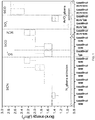
- Figure 1 compares test results obtained through the method of the invention to results obtained through a pre-existing treatment of the bonding surfaces.
- two substrates which may for example be silicon wafers provided with dielectric bonding layers are subjected to the following pre-treatment steps prior to bonding:
- Plasma activation in the present context refers to a process wherein the surface of the substrate is treated by physical sputtering of plasma ions, but without any significant removal of material from the substrate as such, i.e. without etching the surface of the substrate.
- the substrate is not treated by reactive ion etching (RIE).
- RIE reactive ion etching
- the activation steps are configured to remove compounds that are chemically bonded to the surface, such as hydrocarbons, but not to significantly remove material from the surface itself.
- the plasma activation in both plasma steps may be performed in a plasma reactor for capacitively coupled plasma (CCP), comprising a set of electrodes, wherein the first electrode is a planar electrode placed inside a reaction chamber and coupled to a radio-frequency (RF) voltage source and the second electrode is grounded.
- the enclosure that forms the chamber is preferably equally grounded.
- the second electrode may be formed by said enclosure that forms the chamber.
- a substrate to be pre-treated is mounted on the lower electrode (normally on a chuck designed to hold the substrate) and exposed to a plasma generated between the electrodes by the RF power.
- the plasma is generated by creating a vacuum in the reaction chamber and by supplying respectively argon or oxygen to the chamber. Under the influence of the RF power and the continued supply of Ar or O, a plasma is created and maintained between the electrodes.
- the plasma density is dependent on the RF power (the higher the power, the higher the density).
- a capacitively coupled plasma reactor enables the above described physical sputtering of plasma ions onto the wafer surface without reactive ion etching.
- One or both of the plasma steps may however also be performed in an inductively coupled plasma reactor, with the process parameters configured to obtain surface activation in the above-described sense.
- the Ar or O based plasma is generated by an RF power source, between electrodes placed outside the reaction chamber and subsequently introduced in the chamber with the substrate to be treated placed therein.
- the plasma steps are not performed in a microwave plasma reactor.
- ions from the plasma are accelerated to the substrate by a DC bias voltage between the plasma and the RF powered electrode.
- the DC bias voltage is a consequence of the plasma formation and is influenced by the RF frequency.
- the DC bias can also be actively controlled to a desired value via a tuning network coupled between the RF-powered electrode and the RF source.
- a capacitively powered electrode can be used to control the bias of the wafer surface. According to preferred embodiments however, a DC bias voltage between the plasma and the substrate to be treated is not actively applied nor controlled.
- the RF frequency is maximum 300MHz. More preferably, the frequency is between 100KHz and 1MHz. Also, the RF power is preferably low, preferably between 50 and 300 W. Treatment durations during each of the plasma steps are kept low, preferably maximum 1 minute. The plasma steps take place at low temperatures, for example between 15°C and 25°C, and preferably not higher than 60°C.
- the following table summarizes the preferred ranges for the plasma parameters (either performed in a CCP or ICP reactor) applicable in both plasma steps of the method of the invention : Pressure 10 to 1000 mTorr (1.33 to 133.3 Pa) RF power 50 to 300 W RF frequency 100kHz - 300MHz Process time 10 to 60 s Temperature ⁇ 60°C
- the bonding layers are formed of silicon carbon oxide or silicon carbon nitride or silicon carbide, hereafter abbreviated as SiCO or SiCN or SiC, i.e. a layer of SiCO or SiCN or SiC is provided on both substrates and direct bonding is established by a SiCO-SiCO bond or a SiCN-SiCN bond.
- SiCO is defined in the present context as the compound SiC y O z with y between 0.4 and 1.2 and z between 0.2 and 1.0.
- SiCN is defined in the present context by the formula SiC y N z with y between 0.7 and 1.1 and z between 0.1 and 0.4.
- SiCN also includes layers of SiC y N z :H, wherein the 'H' represents hydrogen atoms attached to the SiCN molecules. This may be obtained as a consequence of the precursors used in the deposition method for the SiCN layers.
- SiC is defined in the present context as the compound SiC y with y between 0.4 and 1.4.
- the thickness of the dielectric bonding layers is preferably between 10nm and 1 micron, more preferably between 50nm and 150nm.
- the dielectric layers may be deposited on the substrate in any manner known in the art. They may be deposited directly on a semiconductor wafer or on other layers previously deposited on the wafer.
- the dielectric bonding layers Prior to the sequential plasma treatment according to the invention, are preferably planarized by a suitable planarization process, preferably by Chemical Mechanical Polishing. Planarization is performed according to known processes and to a degree of planarity that is suitable for performing a direct bonding technique. In other words, the invention is not limited by any particular process for producing the bonding layers on the substrates to be bonded, nor by any particular planarization process.
- the final wet surface treatment performed after the oxygen plasma activation, is important for the creation of reactive OH groups on the surfaces which are beneficial for the formation of a strong bond.
- the final wet surface treatment may include or consist of a water rinsing step executed according to known practice, applied for cleaning steps in a separate cleaning module.
- the water rinse performs a cleaning of the surface. High efficiency cleaning techniques such as high pressure cleaning or megasonic cleaning could be incorporated in the water rinsing step.
- the final wet treatment may include or consist of exposing the dielectric bonding layers to a water-containing ambient, also resulting in the creation of reactive OH groups on the bonding surfaces. Thanks to the plasma activation, the SiCN, SiCO or SiC surface turns highly hydrophilic and attracts water molecules with a high affinity interaction.
- alternative cleaning solutions such as diluted APM could also be used to remove other surface contaminants. This may be done before or after the wet treatment step.
- each of the substrates that are to be bonded receives the wet treatment (plus possibly treatment by other cleaning solutions) for less than 300 s, followed by a spin drying process. Tests performed by the inventors have shown that the amount of OH groups after the water rinse is higher when the plasma sequence according to the invention is applied compared to when an N 2 plasma treatment is used.
- the specific plasma sequence of the invention is highly effective due to the high density of carbon dangling bonds on the plasma-treated SiCO, SiCO or SiC surfaces, following the method steps according to the invention. These carbon dangling bonds on the two surfaces form strong carbon-carbon bonds, thereby contributing in an important way to the superior bond strength achieved by the method of the invention.
- the presence of the high amounts of C-dangling bonds is also the reason why the method of the invention achieves high bond strength for SiCN, SiCO and SiC bonding layers, whereas the same method is far less effective when applied to SiO 2 bonding layers.
- Electron-spin-resonance (ESR) monitoring of dangling bonds have been invoked to compare SiCN-SiCN and SiO 2 -SiO 2 bonding strength in terms of the evolution of chemical bond densities at the interface.
- the initial DB density (both carbon and silicon dangling bonds) before bonding was extracted from the specimens after plasma activation by argon plasma followed by oxygen plasma activation, and after rinsing.
- the total DB densities measured on the specimens before bonding were estimated at 2.4 ⁇ 10E14 /cm 2 for SiCN, as opposed to 0.2 ⁇ 10E14/cm 2 for the SiO 2 bonding case.
- the DB densities of SiCN-SiCN bonded specimens decrease to 1.2 ⁇ 10E14/ cm 2 and 0.54 ⁇ 10E14/cm 2 for the post-bond annealing at 200 °C and 250 °C, respectively.
- SiO 2 -SiO 2 there are practically no DB detected after the anneal.
- the bond strength in the case of SiO 2 -SiO 2 bonds is primarily based on the influence of the OH-groups formed on the surfaces. This is the reason why the method of the invention has an important positive impact on the bond strength for the carbon-containing bonding layers SiCN, SiCO and SiC, whereas for SiO 2 bonding layers, this positive impact is not achieved. This will be illustrated by the following test results.
- the inventors have performed comparative tests by treating planarized SiCO and SiCN bonding layers on silicon wafers by the method of the invention, compared to a pre-treatment by N 2 plasma activation. Comparative tests were also done on SiO 2 bonding layers. Tests were performed in a capacitively coupled plasma reactor under the following conditions, and at room temperature. The wet treatment step consisted in a deionized water rinse followed by a spin dry process in a wet cleaning module.
- N2 plasma treatment conditions Pressure 350 mTorr RF power 100W RF frequency 350 kHz Process time 15 s N2 flow 35 sccm* Argon plasma treatment conditions Pressure 350 mTorr RF power 200 W RF frequency 350 kHz Process time 15 s Ar flow 35 sccm* Oxygen plasma treatment conditions Pressure 350 mTorr RF power 200 W RF frequency 350 kHz Process time 15 s Oxygen flow 35 sccm* *The unit sccm stands for standard cubic centimetre per minute, the standard conditions being 0°C and 1atm (101325Pa)
- the post-bond anneal temperature is lower than 400°C, more preferably maximum 350°C, more preferably maximum 250°C, more preferably between 200°C and 250°C.
Landscapes
- Pressure Welding/Diffusion-Bonding (AREA)
- Cleaning Or Drying Semiconductors (AREA)
- Physics & Mathematics (AREA)
- Geometry (AREA)
Abstract
Description
- The present invention is related to direct bonding processes wherein a semiconductor substrate is bonded to another semiconductor substrate by forming chemical bonds between the contact surfaces.
- Direct bonding on wafer level, commonly referred to as 'wafer to wafer' bonding, involves the alignment and contacting at room temperature of two semiconductor wafers, usually silicon wafers provided with dielectric bonding layers, followed by an annealing step, during which step chemical bonds are formed between the bonding layers.
- Current wafer to wafer bonding practice falls in two main categories:
- ∘ The surface of both wafers are blanket, flat unpatterned dielectric bonding layers, such as silicon oxide, silicon nitride or a silicon-carbon-oxide (low-k dielectric) layer.
- ∘ The surface of both wafers are flat, patterned dielectric/metal layers (so called hybrid wafer bonding). The main area fraction is covered by the dielectric material, while other areas are metallic, mainly forming contact pads and metal lines. Bonding between dielectric areas takes place by the same mechanism as described above. Locations where metallic areas overlap can be used to realize electrical contacts between the wafers.
- For both categories, Chemical Mechanical Polishing (CMP) is applied to reduce the roughness of the dielectric layers prior to bonding. Surface treatments are applied such as plasma treatment and ultrasonic or other cleaning techniques. Required post-bond annealing temperatures are generally higher than 400°C in order to reach the desired bond strength. In order to reduce the thermal budget of the bonding process, it is desirable to obtain high strength bonds at lower temperatures. This is particularly important in the field of memory devices.
- The same problems are confronted in the 'die to wafer' bonding processes, wherein a semiconductor chip is bonded to a carrier wafer by direct bonding. In the latter domain, it has been known to apply Silicon Carbon Nitride (SiCN) as the dielectric bonding layer. Reference is made to
US2013/0207268 . However, the cited document fails to describe the bonding process in detail and no information is given on applicable annealing temperatures.US2010/0211849 describes SiCN as a 'bonding aid film' in a direct wafer to wafer bonding process. This process is however open to further improvement in terms of the thermal budget (the post-bonding annealing temperature is 400°C). - Various plasma treatments of dielectric bonding surfaces prior to bonding have been described. A nitrogen-based plasma pre-treatment is known to improve the bond strength. Also sequential plasma treatments have been described. Document
US-A-2005/0173057 for example describes a sequential treatment of Si or SiO2 surfaces by a Reactive Ion Etching (RIE) process under oxygen followed by a microwave plasma under nitrogen. For particular bonding layers, for example SiCN layers, these treatments are insufficient or unsuitable, and improved methods are required for increasing the bond strength. - The invention aims to provide a method for bonding substrates by direct bonding between dielectric bonding layers on the surfaces of the substrates, wherein the bond strength is improved compared to existing techniques. The invention is related to a method according to the appended claims.
- The method of the invention is a method for direct bonding of a first substrate to a second substrate, the first and second substrate comprising dielectric bonding layers, wherein the bonding takes place by bringing the dielectric bonding layers into mutual contact to form a substrate assembly and subjecting the assembly to a post-bond anneal, and wherein both bonding layers are subjected to a pre-treatment prior to bonding, the pre-treatment comprising the following steps performed in the order in which they are stated :
- a first plasma activation step in an inert gas plasma,
- a second plasma activation step in an oxygen plasma,
- a wet surface treatment including a water rinsing step or including an exposure to a water-containing ambient,
- According to an embodiment, one or both of the plasma activation steps takes place in a plasma reactor for capacitively coupled plasma. Alternatively, one or both of the plasma activation steps may take place in a plasma reactor for inductively coupled plasma. According to a preferred embodiment, a DC bias voltage between the substrate and the plasma is not actively applied.
- According to an embodiment, both plasma activation steps take place under the following conditions :
- the plasma is generated by a radio frequency power source,
- Pressure between 1.33 and 133.3 Pa (10 and 1000 mTorr)
- RF frequency between 100KHz and 300MHz
- RF power between 50 W and 300 W
- Temperature lower than 60°C.
- More preferably, the RF frequency for both plasma activation steps is between 100KH and 1MHz.
- The post-bond anneal temperature is preferably lower than 400°C, more preferably between 200°C and 250°C. The inert gas may be argon. According to an embodiment, the wet surface treatment is performed in a timespan lower than under 300s. The method may further comprise an intermediate cleaning step between the first and second plasma activation steps.
-
Figure 1 compares test results obtained through the method of the invention to results obtained through a pre-existing treatment of the bonding surfaces. - According to preferred embodiments of the invention, two substrates which may for example be silicon wafers provided with dielectric bonding layers are subjected to the following pre-treatment steps prior to bonding:
- 1. Argon plasma activation
- 2. Optionally an intermediate cleaning step, preferably comprising at least a water rinsing step, preferably by deionized water,
- 3. Oxygen plasma activation
- 4. Wet surface treatment including rinsing by (preferably deionized) water. Alternatively, the wet treatment may include exposure of the plasma-treated surfaces to a H2O-containing ambient
- Plasma activation in the present context refers to a process wherein the surface of the substrate is treated by physical sputtering of plasma ions, but without any significant removal of material from the substrate as such, i.e. without etching the surface of the substrate. In other words, the substrate is not treated by reactive ion etching (RIE). Through the sputtering of plasma ions, the activation steps are configured to remove compounds that are chemically bonded to the surface, such as hydrocarbons, but not to significantly remove material from the surface itself.
- The plasma activation in both plasma steps may be performed in a plasma reactor for capacitively coupled plasma (CCP), comprising a set of electrodes, wherein the first electrode is a planar electrode placed inside a reaction chamber and coupled to a radio-frequency (RF) voltage source and the second electrode is grounded. The enclosure that forms the chamber is preferably equally grounded. The second electrode may be formed by said enclosure that forms the chamber. A substrate to be pre-treated is mounted on the lower electrode (normally on a chuck designed to hold the substrate) and exposed to a plasma generated between the electrodes by the RF power. For realizing the argon or oxygen plasma activation steps of the method according to the invention, the plasma is generated by creating a vacuum in the reaction chamber and by supplying respectively argon or oxygen to the chamber. Under the influence of the RF power and the continued supply of Ar or O, a plasma is created and maintained between the electrodes. The plasma density is dependent on the RF power (the higher the power, the higher the density).
- The use of a capacitively coupled plasma reactor enables the above described physical sputtering of plasma ions onto the wafer surface without reactive ion etching. One or both of the plasma steps may however also be performed in an inductively coupled plasma reactor, with the process parameters configured to obtain surface activation in the above-described sense. In an ICP reactor, the Ar or O based plasma is generated by an RF power source, between electrodes placed outside the reaction chamber and subsequently introduced in the chamber with the substrate to be treated placed therein. According to preferred embodiments, the plasma steps are not performed in a microwave plasma reactor.
- In a CCP reactor, ions from the plasma are accelerated to the substrate by a DC bias voltage between the plasma and the RF powered electrode. The DC bias voltage is a consequence of the plasma formation and is influenced by the RF frequency. The DC bias can also be actively controlled to a desired value via a tuning network coupled between the RF-powered electrode and the RF source. In the case of ICP, a capacitively powered electrode can be used to control the bias of the wafer surface. According to preferred embodiments however, a DC bias voltage between the plasma and the substrate to be treated is not actively applied nor controlled.
- According to preferred embodiments, the RF frequency is maximum 300MHz. More preferably, the frequency is between 100KHz and 1MHz. Also, the RF power is preferably low, preferably between 50 and 300 W. Treatment durations during each of the plasma steps are kept low, preferably maximum 1 minute. The plasma steps take place at low temperatures, for example between 15°C and 25°C, and preferably not higher than 60°C. The following table summarizes the preferred ranges for the plasma parameters (either performed in a CCP or ICP reactor) applicable in both plasma steps of the method of the invention :
Pressure 10 to 1000 mTorr (1.33 to 133.3 Pa) RF power 50 to 300 W RF frequency 100kHz - 300MHz Process time 10 to 60 s Temperature <60°C - In the method of the invention, the bonding layers are formed of silicon carbon oxide or silicon carbon nitride or silicon carbide, hereafter abbreviated as SiCO or SiCN or SiC, i.e. a layer of SiCO or SiCN or SiC is provided on both substrates and direct bonding is established by a SiCO-SiCO bond or a SiCN-SiCN bond. SiCO is defined in the present context as the compound SiCyOz with y between 0.4 and 1.2 and z between 0.2 and 1.0. SiCN, is defined in the present context by the formula SiCyNz with y between 0.7 and 1.1 and z between 0.1 and 0.4. The term SiCN also includes layers of SiCyNz:H, wherein the 'H' represents hydrogen atoms attached to the SiCN molecules. This may be obtained as a consequence of the precursors used in the deposition method for the SiCN layers. SiC is defined in the present context as the compound SiCy with y between 0.4 and 1.4.
- The thickness of the dielectric bonding layers is preferably between 10nm and 1 micron, more preferably between 50nm and 150nm. The dielectric layers may be deposited on the substrate in any manner known in the art. They may be deposited directly on a semiconductor wafer or on other layers previously deposited on the wafer. Prior to the sequential plasma treatment according to the invention, the dielectric bonding layers are preferably planarized by a suitable planarization process, preferably by Chemical Mechanical Polishing. Planarization is performed according to known processes and to a degree of planarity that is suitable for performing a direct bonding technique. In other words, the invention is not limited by any particular process for producing the bonding layers on the substrates to be bonded, nor by any particular planarization process.
- An intermediate cleaning step between the plasma treatments is optional, as stated above. The final wet surface treatment, performed after the oxygen plasma activation, is important for the creation of reactive OH groups on the surfaces which are beneficial for the formation of a strong bond. The final wet surface treatment may include or consist of a water rinsing step executed according to known practice, applied for cleaning steps in a separate cleaning module. In addition to aiding the formation of OH groups, the water rinse performs a cleaning of the surface. High efficiency cleaning techniques such as high pressure cleaning or megasonic cleaning could be incorporated in the water rinsing step. Instead of a water rinsing step, the final wet treatment may include or consist of exposing the dielectric bonding layers to a water-containing ambient, also resulting in the creation of reactive OH groups on the bonding surfaces. Thanks to the plasma activation, the SiCN, SiCO or SiC surface turns highly hydrophilic and attracts water molecules with a high affinity interaction. In addition to the final wet surface treatment (including water rinsing or exposure to H2O-containing ambient), alternative cleaning solutions such as diluted APM could also be used to remove other surface contaminants. This may be done before or after the wet treatment step. According to preferred embodiments, each of the substrates that are to be bonded receives the wet treatment (plus possibly treatment by other cleaning solutions) for less than 300 s, followed by a spin drying process. Tests performed by the inventors have shown that the amount of OH groups after the water rinse is higher when the plasma sequence according to the invention is applied compared to when an N2 plasma treatment is used.
- In addition to the formation of OH groups, the specific plasma sequence of the invention is highly effective due to the high density of carbon dangling bonds on the plasma-treated SiCO, SiCO or SiC surfaces, following the method steps according to the invention. These carbon dangling bonds on the two surfaces form strong carbon-carbon bonds, thereby contributing in an important way to the superior bond strength achieved by the method of the invention. The presence of the high amounts of C-dangling bonds is also the reason why the method of the invention achieves high bond strength for SiCN, SiCO and SiC bonding layers, whereas the same method is far less effective when applied to SiO2 bonding layers. Electron-spin-resonance (ESR) monitoring of dangling bonds (DB) have been invoked to compare SiCN-SiCN and SiO2-SiO2 bonding strength in terms of the evolution of chemical bond densities at the interface. The initial DB density (both carbon and silicon dangling bonds) before bonding was extracted from the specimens after plasma activation by argon plasma followed by oxygen plasma activation, and after rinsing. The total DB densities measured on the specimens before bonding were estimated at 2.4 × 10E14 /cm2 for SiCN, as opposed to 0.2 × 10E14/cm2 for the SiO2 bonding case. After bonding, the DB densities of SiCN-SiCN bonded specimens decrease to 1.2 × 10E14/ cm2 and 0.54 × 10E14/cm2 for the post-bond annealing at 200 °C and 250 °C, respectively. For SiO2-SiO2, there are practically no DB detected after the anneal. These results illustrate the important contribution of carbon dangling bonds to the bond strength in the case of SiCN. In the case of SiO2, there is no major contribution to the chemical bond formation at the interface of SiO2-SiO2 by the effect of dangling bonds, because of the lower initial DB density prior to bonding. The bond strength in the case of SiO2-SiO2 bonds is primarily based on the influence of the OH-groups formed on the surfaces. This is the reason why the method of the invention has an important positive impact on the bond strength for the carbon-containing bonding layers SiCN, SiCO and SiC, whereas for SiO2 bonding layers, this positive impact is not achieved. This will be illustrated by the following test results.
- The inventors have performed comparative tests by treating planarized SiCO and SiCN bonding layers on silicon wafers by the method of the invention, compared to a pre-treatment by N2 plasma activation. Comparative tests were also done on SiO2 bonding layers. Tests were performed in a capacitively coupled plasma reactor under the following conditions, and at room temperature. The wet treatment step consisted in a deionized water rinse followed by a spin dry process in a wet cleaning module.
N2 plasma treatment conditions Pressure 350 mTorr RF power 100W RF frequency 350 kHz Process time 15 s N2 flow 35 sccm* Argon plasma treatment conditions Pressure 350 mTorr RF power 200 W RF frequency 350 kHz Process time 15 s Ar flow 35 sccm* Oxygen plasma treatment conditions Pressure 350 mTorr RF power 200 W RF frequency 350 kHz Process time 15 s Oxygen flow 35 sccm* *The unit sccm stands for standard cubic centimetre per minute, the standard conditions being 0°C and 1atm (101325Pa) - Direct bonding by SiCO-SiCO bonding, SiCN-SiCN bonding or SiO2-SiO2 bonding was then performed. Post-bond annealing was done during 2 or 4 hours at 200°C, and in some cases at higher temperatures between 210°C and 250°C, as indicated in the graph in
Figure 1. Figure 1 shows the measured bond strength for the various experiments. The squares indicate average values of a number of measurements done for each condition outlined along the X-axis. It is clear that in the case of SiCN and SiCO, the Ar-O2 pre-treatment according to the invention results in higher bond strength compared to the N2-pretreatment applied in combination with the same or similar anneal temperature. Importantly, high bond strength is obtainable after post-bond annealing at a temperature of 200 and 250°C, i.e. lower than the post-bond anneal temperatures generally applied today. This means that the invention opens up potential for obtaining superior bond strength combined with a lower thermal budget. Higher post-bond anneal temperatures are however not excluded from the protection scope. According to an embodiment, the post-bond anneal temperature is lower than 400°C, more preferably maximum 350°C, more preferably maximum 250°C, more preferably between 200°C and 250°C. The results for the SiO2 bonding layers confirm the above-described influence of the increased density of carbon dangling bonds on SiCN and SiCO bonding layers pre-treated by the method of the invention. When applied to SiO2, the method of the invention does not result in increased bonding strength compared to the N2-plasma pre-treatment. - While the invention has been illustrated and described in detail in the drawings and foregoing description, such illustration and description are to be considered illustrative or exemplary and not restrictive. Other variations to the disclosed embodiments can be understood and effected by those skilled in the art in practicing the claimed invention, from a study of the drawings, the disclosure and the appended claims. In the claims, the word "comprising" does not exclude other elements or steps, and the indefinite article "a" or "an" does not exclude a plurality. The mere fact that certain measures are recited in mutually different dependent claims does not indicate that a combination of these measures cannot be used to advantage. Any reference signs in the claims should not be construed as limiting the scope.
Claims (11)
- A method for direct bonding of a first substrate to a second substrate, the first and second substrate comprising dielectric bonding layers, wherein the bonding takes place by bringing the dielectric bonding layers into mutual contact to form a substrate assembly and subjecting the assembly to a post-bond anneal, and wherein both bonding layers are subjected to a pre-treatment prior to bonding, the pre-treatment comprising the following steps performed in the order in which they are stated :• a first plasma activation step in an inert gas plasma,• a second plasma activation step in an oxygen plasma,• a wet surface treatment including a water rinsing step or including an exposure to a water-containing ambient,and wherein the two dielectric bonding layers on the two substrates are two SiCO layers, or two SiCN layer, or two SiC layers.
- The method according to claim 1, wherein one or both of the plasma activation steps takes place in a plasma reactor for capacitively coupled plasma.
- The method according to claim 1, wherein one or both of the plasma activation steps takes place in a plasma reactor for inductively coupled plasma.
- The method according to any one of the preceding claims, wherein a DC bias voltage between the substrate and the plasma is not actively applied.
- The method according to any one of the preceding claims, wherein both plasma activation steps take place under the following conditions :• the plasma is generated by a radio frequency power source,• Pressure between 1.33 and 133.3 Pa• RF frequency between 100KHz and 300MHz• RF power between 50 W and 300 W• Temperature lower than 60°C.
- The method according to claim 5, wherein the RF frequency for both plasma activation steps is between 100KH and 1MHz.
- The method according to any one of the preceding claims, wherein the post-bond anneal temperature is lower than 400°C.
- The method according to claim 7, wherein the post-bond anneal temperature is between 200°C and 250°C.
- The method according to any one of the preceding claims, wherein the inert gas is argon.
- The method according to any one of the preceding claims, wherein the wet surface treatment is performed in a timespan lower than under 300s.
- The method according to any one of the preceding claims, comprising an intermediate cleaning step between the first and second plasma activation steps.
Applications Claiming Priority (1)
| Application Number | Priority Date | Filing Date | Title |
|---|---|---|---|
| EP17158430.3A EP3367425A1 (en) | 2017-02-28 | 2017-02-28 | A method for direct bonding of semiconductor substrates |
Publications (2)
| Publication Number | Publication Date |
|---|---|
| EP3376524A1 true EP3376524A1 (en) | 2018-09-19 |
| EP3376524B1 EP3376524B1 (en) | 2021-12-15 |
Family
ID=58192191
Family Applications (2)
| Application Number | Title | Priority Date | Filing Date |
|---|---|---|---|
| EP17158430.3A Withdrawn EP3367425A1 (en) | 2017-02-28 | 2017-02-28 | A method for direct bonding of semiconductor substrates |
| EP18157833.7A Active EP3376524B1 (en) | 2017-02-28 | 2018-02-21 | A method for direct bonding of semiconductor substrates |
Family Applications Before (1)
| Application Number | Title | Priority Date | Filing Date |
|---|---|---|---|
| EP17158430.3A Withdrawn EP3367425A1 (en) | 2017-02-28 | 2017-02-28 | A method for direct bonding of semiconductor substrates |
Country Status (3)
| Country | Link |
|---|---|
| US (1) | US10886252B2 (en) |
| EP (2) | EP3367425A1 (en) |
| CN (1) | CN108511332B (en) |
Families Citing this family (7)
| Publication number | Priority date | Publication date | Assignee | Title |
|---|---|---|---|---|
| CN112885777B (en) * | 2020-01-07 | 2022-12-09 | 长江存储科技有限责任公司 | Metal-dielectric bonding method and structure |
| CN115602651B (en) | 2021-07-09 | 2025-12-09 | 联华电子股份有限公司 | Bonded semiconductor structure and method of making the same |
| US12469683B2 (en) | 2021-09-27 | 2025-11-11 | Applied Materials Inc. | Water vapor plasma to enhance surface hydrophilicity |
| KR20230105177A (en) | 2022-01-03 | 2023-07-11 | 삼성전자주식회사 | Apparatus for plasma treatment, substrate bonding system including the same and substrate bonding method using the same |
| CN114920468B (en) * | 2022-06-01 | 2023-12-05 | 北方夜视技术股份有限公司 | Borosilicate glass hydrophilic bonding method |
| CN115262211B (en) * | 2022-07-15 | 2023-08-29 | 南方科技大学 | A kind of superhydrophobic fabric and preparation method thereof |
| CN116053118A (en) * | 2022-12-09 | 2023-05-02 | 湖南三安半导体有限责任公司 | A bonding method for SiC substrate |
Citations (4)
| Publication number | Priority date | Publication date | Assignee | Title |
|---|---|---|---|---|
| EP1518669A2 (en) * | 2003-08-29 | 2005-03-30 | Tadatomo Suga | Method for bonding substrates and method for irradiating particle beam to be utilized therefor |
| US20100211849A1 (en) | 2009-02-19 | 2010-08-19 | Nec Laboratories America, Inc. | Multi-dimensional ldpc coded modulation for high-speed optical transmission systems |
| US20130207268A1 (en) | 2012-02-14 | 2013-08-15 | Stmicroelectronics (Crolles 2) Sas | Chip assembly system |
| EP3024019A1 (en) * | 2014-11-24 | 2016-05-25 | IMEC vzw | Method for direct bonding of semiconductor substrates. |
Family Cites Families (20)
| Publication number | Priority date | Publication date | Assignee | Title |
|---|---|---|---|---|
| US6171982B1 (en) * | 1997-12-26 | 2001-01-09 | Canon Kabushiki Kaisha | Method and apparatus for heat-treating an SOI substrate and method of preparing an SOI substrate by using the same |
| US6380096B2 (en) * | 1998-07-09 | 2002-04-30 | Applied Materials, Inc. | In-situ integrated oxide etch process particularly useful for copper dual damascene |
| US6365062B1 (en) * | 1999-05-07 | 2002-04-02 | United Microelectronics Corp. | Treatment on silicon oxynitride |
| US6563133B1 (en) * | 2000-08-09 | 2003-05-13 | Ziptronix, Inc. | Method of epitaxial-like wafer bonding at low temperature and bonded structure |
| US20030089950A1 (en) * | 2001-11-15 | 2003-05-15 | Kuech Thomas F. | Bonding of silicon and silicon-germanium to insulating substrates |
| US20040126993A1 (en) * | 2002-12-30 | 2004-07-01 | Chan Kevin K. | Low temperature fusion bonding with high surface energy using a wet chemical treatment |
| US7109092B2 (en) * | 2003-05-19 | 2006-09-19 | Ziptronix, Inc. | Method of room temperature covalent bonding |
| US6830962B1 (en) * | 2003-08-05 | 2004-12-14 | International Business Machines Corporation | Self-aligned SOI with different crystal orientation using wafer bonding and SIMOX processes |
| US7357977B2 (en) * | 2005-01-13 | 2008-04-15 | International Business Machines Corporation | Ultralow dielectric constant layer with controlled biaxial stress |
| US20070015373A1 (en) * | 2005-07-13 | 2007-01-18 | General Electric Company | Semiconductor device and method of processing a semiconductor substrate |
| JP2007281062A (en) * | 2006-04-04 | 2007-10-25 | Hitachi Ltd | Electronic component assembly, electronic circuit module using the same, and manufacturing method thereof |
| DE102009020163B4 (en) * | 2009-05-07 | 2012-07-19 | Fraunhofer-Gesellschaft zur Förderung der angewandten Forschung e.V. | Method for interlayer-free bonding of substrates, apparatus for carrying out a plasma treatment and their use |
| FR2963158B1 (en) * | 2010-07-21 | 2013-05-17 | Commissariat Energie Atomique | DIRECT COLLAGE ASSEMBLY METHOD BETWEEN TWO ELEMENTS COMPRISING COPPER PORTIONS AND DIELECTRIC MATERIALS |
| KR20130135261A (en) * | 2010-11-03 | 2013-12-10 | 어플라이드 머티어리얼스, 인코포레이티드 | Apparatus and methods for deposition of silicon carbide and silicon carbonitride films |
| US8975158B2 (en) * | 2011-04-08 | 2015-03-10 | Ev Group E. Thallner Gmbh | Method for permanently bonding wafers |
| TW201319299A (en) * | 2011-09-13 | 2013-05-16 | 應用材料股份有限公司 | Activated ruthenium precursor for low temperature plasma assisted deposition |
| CN104685633B (en) * | 2012-07-03 | 2018-08-03 | Imec 非营利协会 | The method for making thin film transistor (TFT) |
| EP2819162B1 (en) * | 2013-06-24 | 2020-06-17 | IMEC vzw | Method for producing contact areas on a semiconductor substrate |
| EP3035369B1 (en) * | 2014-12-18 | 2020-11-25 | IMEC vzw | Plasma treatment method |
| WO2017155806A1 (en) * | 2016-03-07 | 2017-09-14 | Sunedison Semiconductor Limited | Semiconductor on insulator structure comprising a plasma oxide layer and method of manufacture thereof |
-
2017
- 2017-02-28 EP EP17158430.3A patent/EP3367425A1/en not_active Withdrawn
-
2018
- 2018-02-21 EP EP18157833.7A patent/EP3376524B1/en active Active
- 2018-02-28 US US15/908,641 patent/US10886252B2/en active Active
- 2018-02-28 CN CN201810167581.6A patent/CN108511332B/en active Active
Patent Citations (5)
| Publication number | Priority date | Publication date | Assignee | Title |
|---|---|---|---|---|
| EP1518669A2 (en) * | 2003-08-29 | 2005-03-30 | Tadatomo Suga | Method for bonding substrates and method for irradiating particle beam to be utilized therefor |
| US20050173057A1 (en) | 2003-08-29 | 2005-08-11 | Tadatomo Suga | Method for bonding substrates and method for irradiating particle beam to be utilized therefor |
| US20100211849A1 (en) | 2009-02-19 | 2010-08-19 | Nec Laboratories America, Inc. | Multi-dimensional ldpc coded modulation for high-speed optical transmission systems |
| US20130207268A1 (en) | 2012-02-14 | 2013-08-15 | Stmicroelectronics (Crolles 2) Sas | Chip assembly system |
| EP3024019A1 (en) * | 2014-11-24 | 2016-05-25 | IMEC vzw | Method for direct bonding of semiconductor substrates. |
Non-Patent Citations (2)
| Title |
|---|
| EDWARD M. LISTON: "Plasma Treatment for Improved Bonding: A Review", THE JOURNAL OF ADHESION, vol. 30, no. 1-4, 1 January 1989 (1989-01-01), US, pages 199 - 218, XP055398489, ISSN: 0021-8464, DOI: 10.1080/00218468908048206 * |
| SUNI T ET AL: "EFFECTS OF PLASMA ACTIVATION ON HYDROPHOLIC BONDING OF SI AND SIO2", JOURNAL OF THE ELECTROCHEMICAL SOC, ELECTROCHEMICAL SOCIETY, INC, US, vol. 149, no. 6, 1 June 2002 (2002-06-01), pages G348 - G351, XP008046162, ISSN: 0013-4651, DOI: 10.1149/1.1477209 * |
Also Published As
| Publication number | Publication date |
|---|---|
| US10886252B2 (en) | 2021-01-05 |
| US20180247914A1 (en) | 2018-08-30 |
| EP3367425A1 (en) | 2018-08-29 |
| EP3376524B1 (en) | 2021-12-15 |
| CN108511332A (en) | 2018-09-07 |
| CN108511332B (en) | 2023-06-20 |
Similar Documents
| Publication | Publication Date | Title |
|---|---|---|
| EP3376524B1 (en) | A method for direct bonding of semiconductor substrates | |
| US12557615B2 (en) | Methods for bonding semiconductor elements | |
| JP4379943B2 (en) | Semiconductor substrate manufacturing method and semiconductor substrate manufacturing apparatus | |
| JP4927080B2 (en) | Method for reducing the roughness of thick insulating layers | |
| CN101536155B (en) | Plasma dielectric etch process including in-situ backside polymer removal for low-dielectric constant material | |
| JP4919871B2 (en) | Etching method, semiconductor device manufacturing method, and storage medium | |
| US7776719B2 (en) | Method for manufacturing bonded wafer | |
| JP6036732B2 (en) | Manufacturing method of bonded wafer | |
| KR20100073974A (en) | Method for bonding two substrates | |
| JP4627262B2 (en) | Method for forming low dielectric constant film | |
| JP2020520554A (en) | Precleaning and deposition methods for superconductor interconnects | |
| JP2004063521A (en) | Method for manufacturing semiconductor device | |
| JP2000216249A (en) | Electronic device manufacturing method and device | |
| US9082819B2 (en) | Process for thinning the active silicon layer of a substrate of “silicon on insulator” (SOI) type | |
| JP2012015411A (en) | Semiconductor device manufacturing method and semiconductor device | |
| CN108475632B (en) | Substrate processing method | |
| CN116110848A (en) | Bonding method of germanium-on-insulator substrate | |
| EP3029730B1 (en) | Bonded wafer manufacturing method | |
| JP4515309B2 (en) | Etching method | |
| JPH07245382A (en) | Method for manufacturing composite element and bonded substrate | |
| TW559933B (en) | An apparatus and a method for reducing copper oxide on a copper layer | |
| JPH08130199A (en) | Method of flattening stepped substrate | |
| KR20250110746A (en) | Method for low temperature bonding of substrates | |
| KR20260025060A (en) | Hybrid Bonding Manufacturing Method using Dry Etching | |
| KR101017758B1 (en) | Method of forming nitride film of semiconductor device |
Legal Events
| Date | Code | Title | Description |
|---|---|---|---|
| PUAI | Public reference made under article 153(3) epc to a published international application that has entered the european phase |
Free format text: ORIGINAL CODE: 0009012 |
|
| STAA | Information on the status of an ep patent application or granted ep patent |
Free format text: STATUS: THE APPLICATION HAS BEEN PUBLISHED |
|
| AK | Designated contracting states |
Kind code of ref document: A1 Designated state(s): AL AT BE BG CH CY CZ DE DK EE ES FI FR GB GR HR HU IE IS IT LI LT LU LV MC MK MT NL NO PL PT RO RS SE SI SK SM TR |
|
| AX | Request for extension of the european patent |
Extension state: BA ME |
|
| STAA | Information on the status of an ep patent application or granted ep patent |
Free format text: STATUS: REQUEST FOR EXAMINATION WAS MADE |
|
| 17P | Request for examination filed |
Effective date: 20190312 |
|
| RBV | Designated contracting states (corrected) |
Designated state(s): AL AT BE BG CH CY CZ DE DK EE ES FI FR GB GR HR HU IE IS IT LI LT LU LV MC MK MT NL NO PL PT RO RS SE SI SK SM TR |
|
| REG | Reference to a national code |
Ref country code: DE Ref legal event code: R079 Ref document number: 602018028071 Country of ref document: DE Free format text: PREVIOUS MAIN CLASS: H01L0021200000 Ipc: H01L0021180000 |
|
| RIC1 | Information provided on ipc code assigned before grant |
Ipc: H01L 21/18 20060101AFI20210520BHEP Ipc: H01J 37/32 20060101ALN20210520BHEP |
|
| GRAP | Despatch of communication of intention to grant a patent |
Free format text: ORIGINAL CODE: EPIDOSNIGR1 |
|
| STAA | Information on the status of an ep patent application or granted ep patent |
Free format text: STATUS: GRANT OF PATENT IS INTENDED |
|
| INTG | Intention to grant announced |
Effective date: 20210630 |
|
| GRAS | Grant fee paid |
Free format text: ORIGINAL CODE: EPIDOSNIGR3 |
|
| GRAA | (expected) grant |
Free format text: ORIGINAL CODE: 0009210 |
|
| STAA | Information on the status of an ep patent application or granted ep patent |
Free format text: STATUS: THE PATENT HAS BEEN GRANTED |
|
| AK | Designated contracting states |
Kind code of ref document: B1 Designated state(s): AL AT BE BG CH CY CZ DE DK EE ES FI FR GB GR HR HU IE IS IT LI LT LU LV MC MK MT NL NO PL PT RO RS SE SI SK SM TR |
|
| REG | Reference to a national code |
Ref country code: GB Ref legal event code: FG4D Ref country code: CH Ref legal event code: EP |
|
| REG | Reference to a national code |
Ref country code: IE Ref legal event code: FG4D Ref country code: DE Ref legal event code: R096 Ref document number: 602018028071 Country of ref document: DE |
|
| REG | Reference to a national code |
Ref country code: AT Ref legal event code: REF Ref document number: 1456118 Country of ref document: AT Kind code of ref document: T Effective date: 20220115 |
|
| REG | Reference to a national code |
Ref country code: LT Ref legal event code: MG9D |
|
| REG | Reference to a national code |
Ref country code: NL Ref legal event code: MP Effective date: 20211215 |
|
| PG25 | Lapsed in a contracting state [announced via postgrant information from national office to epo] |
Ref country code: RS Free format text: LAPSE BECAUSE OF FAILURE TO SUBMIT A TRANSLATION OF THE DESCRIPTION OR TO PAY THE FEE WITHIN THE PRESCRIBED TIME-LIMIT Effective date: 20211215 Ref country code: LT Free format text: LAPSE BECAUSE OF FAILURE TO SUBMIT A TRANSLATION OF THE DESCRIPTION OR TO PAY THE FEE WITHIN THE PRESCRIBED TIME-LIMIT Effective date: 20211215 Ref country code: FI Free format text: LAPSE BECAUSE OF FAILURE TO SUBMIT A TRANSLATION OF THE DESCRIPTION OR TO PAY THE FEE WITHIN THE PRESCRIBED TIME-LIMIT Effective date: 20211215 Ref country code: BG Free format text: LAPSE BECAUSE OF FAILURE TO SUBMIT A TRANSLATION OF THE DESCRIPTION OR TO PAY THE FEE WITHIN THE PRESCRIBED TIME-LIMIT Effective date: 20220315 |
|
| REG | Reference to a national code |
Ref country code: AT Ref legal event code: MK05 Ref document number: 1456118 Country of ref document: AT Kind code of ref document: T Effective date: 20211215 |
|
| PG25 | Lapsed in a contracting state [announced via postgrant information from national office to epo] |
Ref country code: SE Free format text: LAPSE BECAUSE OF FAILURE TO SUBMIT A TRANSLATION OF THE DESCRIPTION OR TO PAY THE FEE WITHIN THE PRESCRIBED TIME-LIMIT Effective date: 20211215 Ref country code: NO Free format text: LAPSE BECAUSE OF FAILURE TO SUBMIT A TRANSLATION OF THE DESCRIPTION OR TO PAY THE FEE WITHIN THE PRESCRIBED TIME-LIMIT Effective date: 20220315 Ref country code: LV Free format text: LAPSE BECAUSE OF FAILURE TO SUBMIT A TRANSLATION OF THE DESCRIPTION OR TO PAY THE FEE WITHIN THE PRESCRIBED TIME-LIMIT Effective date: 20211215 Ref country code: HR Free format text: LAPSE BECAUSE OF FAILURE TO SUBMIT A TRANSLATION OF THE DESCRIPTION OR TO PAY THE FEE WITHIN THE PRESCRIBED TIME-LIMIT Effective date: 20211215 Ref country code: GR Free format text: LAPSE BECAUSE OF FAILURE TO SUBMIT A TRANSLATION OF THE DESCRIPTION OR TO PAY THE FEE WITHIN THE PRESCRIBED TIME-LIMIT Effective date: 20220316 |
|
| PG25 | Lapsed in a contracting state [announced via postgrant information from national office to epo] |
Ref country code: NL Free format text: LAPSE BECAUSE OF FAILURE TO SUBMIT A TRANSLATION OF THE DESCRIPTION OR TO PAY THE FEE WITHIN THE PRESCRIBED TIME-LIMIT Effective date: 20211215 |
|
| PG25 | Lapsed in a contracting state [announced via postgrant information from national office to epo] |
Ref country code: SM Free format text: LAPSE BECAUSE OF FAILURE TO SUBMIT A TRANSLATION OF THE DESCRIPTION OR TO PAY THE FEE WITHIN THE PRESCRIBED TIME-LIMIT Effective date: 20211215 Ref country code: SK Free format text: LAPSE BECAUSE OF FAILURE TO SUBMIT A TRANSLATION OF THE DESCRIPTION OR TO PAY THE FEE WITHIN THE PRESCRIBED TIME-LIMIT Effective date: 20211215 Ref country code: RO Free format text: LAPSE BECAUSE OF FAILURE TO SUBMIT A TRANSLATION OF THE DESCRIPTION OR TO PAY THE FEE WITHIN THE PRESCRIBED TIME-LIMIT Effective date: 20211215 Ref country code: PT Free format text: LAPSE BECAUSE OF FAILURE TO SUBMIT A TRANSLATION OF THE DESCRIPTION OR TO PAY THE FEE WITHIN THE PRESCRIBED TIME-LIMIT Effective date: 20220418 Ref country code: ES Free format text: LAPSE BECAUSE OF FAILURE TO SUBMIT A TRANSLATION OF THE DESCRIPTION OR TO PAY THE FEE WITHIN THE PRESCRIBED TIME-LIMIT Effective date: 20211215 Ref country code: EE Free format text: LAPSE BECAUSE OF FAILURE TO SUBMIT A TRANSLATION OF THE DESCRIPTION OR TO PAY THE FEE WITHIN THE PRESCRIBED TIME-LIMIT Effective date: 20211215 Ref country code: CZ Free format text: LAPSE BECAUSE OF FAILURE TO SUBMIT A TRANSLATION OF THE DESCRIPTION OR TO PAY THE FEE WITHIN THE PRESCRIBED TIME-LIMIT Effective date: 20211215 |
|
| PG25 | Lapsed in a contracting state [announced via postgrant information from national office to epo] |
Ref country code: PL Free format text: LAPSE BECAUSE OF FAILURE TO SUBMIT A TRANSLATION OF THE DESCRIPTION OR TO PAY THE FEE WITHIN THE PRESCRIBED TIME-LIMIT Effective date: 20211215 Ref country code: AT Free format text: LAPSE BECAUSE OF FAILURE TO SUBMIT A TRANSLATION OF THE DESCRIPTION OR TO PAY THE FEE WITHIN THE PRESCRIBED TIME-LIMIT Effective date: 20211215 |
|
| REG | Reference to a national code |
Ref country code: DE Ref legal event code: R097 Ref document number: 602018028071 Country of ref document: DE |
|
| PG25 | Lapsed in a contracting state [announced via postgrant information from national office to epo] |
Ref country code: MC Free format text: LAPSE BECAUSE OF FAILURE TO SUBMIT A TRANSLATION OF THE DESCRIPTION OR TO PAY THE FEE WITHIN THE PRESCRIBED TIME-LIMIT Effective date: 20211215 Ref country code: IS Free format text: LAPSE BECAUSE OF FAILURE TO SUBMIT A TRANSLATION OF THE DESCRIPTION OR TO PAY THE FEE WITHIN THE PRESCRIBED TIME-LIMIT Effective date: 20220415 |
|
| REG | Reference to a national code |
Ref country code: CH Ref legal event code: PL |
|
| PLBE | No opposition filed within time limit |
Free format text: ORIGINAL CODE: 0009261 |
|
| STAA | Information on the status of an ep patent application or granted ep patent |
Free format text: STATUS: NO OPPOSITION FILED WITHIN TIME LIMIT |
|
| REG | Reference to a national code |
Ref country code: BE Ref legal event code: MM Effective date: 20220228 |
|
| PG25 | Lapsed in a contracting state [announced via postgrant information from national office to epo] |
Ref country code: LU Free format text: LAPSE BECAUSE OF NON-PAYMENT OF DUE FEES Effective date: 20220221 Ref country code: DK Free format text: LAPSE BECAUSE OF FAILURE TO SUBMIT A TRANSLATION OF THE DESCRIPTION OR TO PAY THE FEE WITHIN THE PRESCRIBED TIME-LIMIT Effective date: 20211215 Ref country code: AL Free format text: LAPSE BECAUSE OF FAILURE TO SUBMIT A TRANSLATION OF THE DESCRIPTION OR TO PAY THE FEE WITHIN THE PRESCRIBED TIME-LIMIT Effective date: 20211215 |
|
| 26N | No opposition filed |
Effective date: 20220916 |
|
| GBPC | Gb: european patent ceased through non-payment of renewal fee |
Effective date: 20220315 |
|
| PG25 | Lapsed in a contracting state [announced via postgrant information from national office to epo] |
Ref country code: SI Free format text: LAPSE BECAUSE OF FAILURE TO SUBMIT A TRANSLATION OF THE DESCRIPTION OR TO PAY THE FEE WITHIN THE PRESCRIBED TIME-LIMIT Effective date: 20211215 |
|
| PG25 | Lapsed in a contracting state [announced via postgrant information from national office to epo] |
Ref country code: FR Free format text: LAPSE BECAUSE OF NON-PAYMENT OF DUE FEES Effective date: 20220228 |
|
| PG25 | Lapsed in a contracting state [announced via postgrant information from national office to epo] |
Ref country code: LI Free format text: LAPSE BECAUSE OF NON-PAYMENT OF DUE FEES Effective date: 20220228 Ref country code: IE Free format text: LAPSE BECAUSE OF NON-PAYMENT OF DUE FEES Effective date: 20220221 Ref country code: GB Free format text: LAPSE BECAUSE OF NON-PAYMENT OF DUE FEES Effective date: 20220315 Ref country code: CH Free format text: LAPSE BECAUSE OF NON-PAYMENT OF DUE FEES Effective date: 20220228 |
|
| PG25 | Lapsed in a contracting state [announced via postgrant information from national office to epo] |
Ref country code: BE Free format text: LAPSE BECAUSE OF NON-PAYMENT OF DUE FEES Effective date: 20220228 |
|
| PG25 | Lapsed in a contracting state [announced via postgrant information from national office to epo] |
Ref country code: IT Free format text: LAPSE BECAUSE OF FAILURE TO SUBMIT A TRANSLATION OF THE DESCRIPTION OR TO PAY THE FEE WITHIN THE PRESCRIBED TIME-LIMIT Effective date: 20211215 |
|
| P01 | Opt-out of the competence of the unified patent court (upc) registered |
Effective date: 20230513 |
|
| PG25 | Lapsed in a contracting state [announced via postgrant information from national office to epo] |
Ref country code: HU Free format text: LAPSE BECAUSE OF FAILURE TO SUBMIT A TRANSLATION OF THE DESCRIPTION OR TO PAY THE FEE WITHIN THE PRESCRIBED TIME-LIMIT; INVALID AB INITIO Effective date: 20180221 |
|
| PG25 | Lapsed in a contracting state [announced via postgrant information from national office to epo] |
Ref country code: MK Free format text: LAPSE BECAUSE OF FAILURE TO SUBMIT A TRANSLATION OF THE DESCRIPTION OR TO PAY THE FEE WITHIN THE PRESCRIBED TIME-LIMIT Effective date: 20211215 Ref country code: CY Free format text: LAPSE BECAUSE OF FAILURE TO SUBMIT A TRANSLATION OF THE DESCRIPTION OR TO PAY THE FEE WITHIN THE PRESCRIBED TIME-LIMIT Effective date: 20211215 |
|
| PG25 | Lapsed in a contracting state [announced via postgrant information from national office to epo] |
Ref country code: TR Free format text: LAPSE BECAUSE OF FAILURE TO SUBMIT A TRANSLATION OF THE DESCRIPTION OR TO PAY THE FEE WITHIN THE PRESCRIBED TIME-LIMIT Effective date: 20211215 |
|
| PG25 | Lapsed in a contracting state [announced via postgrant information from national office to epo] |
Ref country code: MT Free format text: LAPSE BECAUSE OF FAILURE TO SUBMIT A TRANSLATION OF THE DESCRIPTION OR TO PAY THE FEE WITHIN THE PRESCRIBED TIME-LIMIT Effective date: 20211215 |
|
| REG | Reference to a national code |
Ref country code: DE Ref legal event code: R079 Ref document number: 602018028071 Country of ref document: DE Free format text: PREVIOUS MAIN CLASS: H01L0021180000 Ipc: H10P0014000000 |
|
| PGFP | Annual fee paid to national office [announced via postgrant information from national office to epo] |
Ref country code: DE Payment date: 20260121 Year of fee payment: 9 |