EP3375615A1 - Druckerchip, tintenpatrone und verfahren zur zuteilung eines datenspeichers zu einem druckerchip - Google Patents
Druckerchip, tintenpatrone und verfahren zur zuteilung eines datenspeichers zu einem druckerchip Download PDFInfo
- Publication number
- EP3375615A1 EP3375615A1 EP16863459.0A EP16863459A EP3375615A1 EP 3375615 A1 EP3375615 A1 EP 3375615A1 EP 16863459 A EP16863459 A EP 16863459A EP 3375615 A1 EP3375615 A1 EP 3375615A1
- Authority
- EP
- European Patent Office
- Prior art keywords
- data
- printer
- chip
- storage unit
- data storage
- Prior art date
- Legal status (The legal status is an assumption and is not a legal conclusion. Google has not performed a legal analysis and makes no representation as to the accuracy of the status listed.)
- Granted
Links
Images

Classifications
-
- H—ELECTRICITY
- H04—ELECTRIC COMMUNICATION TECHNIQUE
- H04L—TRANSMISSION OF DIGITAL INFORMATION, e.g. TELEGRAPHIC COMMUNICATION
- H04L63/00—Network architectures or network communication protocols for network security
- H04L63/10—Network architectures or network communication protocols for network security for controlling access to devices or network resources
-
- B—PERFORMING OPERATIONS; TRANSPORTING
- B41—PRINTING; LINING MACHINES; TYPEWRITERS; STAMPS
- B41J—TYPEWRITERS; SELECTIVE PRINTING MECHANISMS, i.e. MECHANISMS PRINTING OTHERWISE THAN FROM A FORME; CORRECTION OF TYPOGRAPHICAL ERRORS
- B41J2/00—Typewriters or selective printing mechanisms characterised by the printing or marking process for which they are designed
- B41J2/005—Typewriters or selective printing mechanisms characterised by the printing or marking process for which they are designed characterised by bringing liquid or particles selectively into contact with a printing material
- B41J2/01—Ink jet
- B41J2/17—Ink jet characterised by ink handling
- B41J2/175—Ink supply systems ; Circuit parts therefor
- B41J2/17503—Ink cartridges
- B41J2/17543—Cartridge presence detection or type identification
- B41J2/17546—Cartridge presence detection or type identification electronically
-
- G—PHYSICS
- G06—COMPUTING OR CALCULATING; COUNTING
- G06F—ELECTRIC DIGITAL DATA PROCESSING
- G06F12/00—Accessing, addressing or allocating within memory systems or architectures
- G06F12/14—Protection against unauthorised use of memory or access to memory
- G06F12/1416—Protection against unauthorised use of memory or access to memory by checking the object accessibility, e.g. type of access defined by the memory independently of subject rights
- G06F12/1425—Protection against unauthorised use of memory or access to memory by checking the object accessibility, e.g. type of access defined by the memory independently of subject rights the protection being physical, e.g. cell, word, block
- G06F12/1433—Protection against unauthorised use of memory or access to memory by checking the object accessibility, e.g. type of access defined by the memory independently of subject rights the protection being physical, e.g. cell, word, block for a module or a part of a module
-
- G—PHYSICS
- G06—COMPUTING OR CALCULATING; COUNTING
- G06F—ELECTRIC DIGITAL DATA PROCESSING
- G06F12/00—Accessing, addressing or allocating within memory systems or architectures
- G06F12/14—Protection against unauthorised use of memory or access to memory
- G06F12/1416—Protection against unauthorised use of memory or access to memory by checking the object accessibility, e.g. type of access defined by the memory independently of subject rights
- G06F12/1425—Protection against unauthorised use of memory or access to memory by checking the object accessibility, e.g. type of access defined by the memory independently of subject rights the protection being physical, e.g. cell, word, block
- G06F12/1441—Protection against unauthorised use of memory or access to memory by checking the object accessibility, e.g. type of access defined by the memory independently of subject rights the protection being physical, e.g. cell, word, block for a range
-
- G—PHYSICS
- G06—COMPUTING OR CALCULATING; COUNTING
- G06F—ELECTRIC DIGITAL DATA PROCESSING
- G06F21/00—Security arrangements for protecting computers, components thereof, programs or data against unauthorised activity
- G06F21/30—Authentication, i.e. establishing the identity or authorisation of security principals
- G06F21/44—Program or device authentication
-
- G—PHYSICS
- G06—COMPUTING OR CALCULATING; COUNTING
- G06F—ELECTRIC DIGITAL DATA PROCESSING
- G06F21/00—Security arrangements for protecting computers, components thereof, programs or data against unauthorised activity
- G06F21/70—Protecting specific internal or peripheral components, in which the protection of a component leads to protection of the entire computer
- G06F21/78—Protecting specific internal or peripheral components, in which the protection of a component leads to protection of the entire computer to assure secure storage of data
-
- H—ELECTRICITY
- H04—ELECTRIC COMMUNICATION TECHNIQUE
- H04L—TRANSMISSION OF DIGITAL INFORMATION, e.g. TELEGRAPHIC COMMUNICATION
- H04L63/00—Network architectures or network communication protocols for network security
- H04L63/08—Network architectures or network communication protocols for network security for authentication of entities
-
- G—PHYSICS
- G06—COMPUTING OR CALCULATING; COUNTING
- G06F—ELECTRIC DIGITAL DATA PROCESSING
- G06F2212/00—Indexing scheme relating to accessing, addressing or allocation within memory systems or architectures
- G06F2212/10—Providing a specific technical effect
- G06F2212/1052—Security improvement
Definitions
- the invention relates to the field of ink-jet printing, in particular to a printer chip, an ink cartridge and a printer chip storage allocation method.
- printing equipment With the popularization of office automation, printing equipment has become indispensable equipment for office activities, common printing equipment includes laser printing equipment and ink-jet printing equipment, and during ink-jet printing, an ink-jet printer and an ink cartridge mounted in the printer are included.
- consumables such as the ink cartridge need to be replaced periodically.
- the ink cartridge needs to be replaced when ink in the ink cartridge is used up
- the replaceable equipment such as the ink cartridge includes printing parameters
- the printing parameters are generally stored in a chip
- the printer chip is mounted in the replaceable equipment such as the ink cartridge so that a printer main body can obtain the data in the first time every time the replaceable equipment is replaced, and thus a good printing effect is guaranteed.
- the information is generally written into the printer chip once, which means that the chip can only be used once and cannot be used repeatedly, and thus the use value of the chip is decreased.
- a printer chip comprises a chip control circuit, a data storage unit used for storing data, and a communication unit used for communication with a printer, wherein the data storage unit and the communication unit are electrically connected with the chip control circuit respectively;
- the printer chip is characterized in that:
- the printer chip is mounted on a replaceable component, the replaceable component is not authorized specifically in an ordinary service state, namely data on the authorization flag bit make the data storage unit in the non-authorized state, the data storage unit is divided into a plurality of areas at the moment and at least comprises the non-protected part, the protected part and the disposable part, and the three parts are different on the aspect of reading and writing permissions;
- the non-protected part allows data to be read and written therein by printing equipment such as the printer main body and is a common data operation port, data stored in the protected part are input when used for the first time, can only be read and cannot be modified or written in, for example, when the printer chip is mounted on an ink cartridge, data stored in the protected part can be the first service date of the ink cartridge, the data can only be read and cannot be modified once being written in, and a user can speculate the effective service life of the ink cartridge according to the first service date of the ink cartridge; the disposable part allows data to be written therein, however, writing can be conducted
- the disposable part when the data storage unit is in the non-authorized state, the disposable part includes the ink cartridge maximum volume data.
- the disposable part when the data storage unit is in the non-authorized state, the disposable part further includes ink cartridge protector serial number data and protection start bit data.
- the protected part when the data storage unit is in the non-authorized state, the protected part includes the ink cartridge first service date.
- the operation unit carries out operation through data sent from the printer main body and the key data stored in the key unit according to the AES algorithm or the DES algorithm or the EDES algorithm or the 3DES algorithm.
- An ink cartridge is provided with the printer chip described above.
- a printing head is provided with the printer chip.
- a printer comprises the printing head and the ink cartridge, wherein the printing head is provided with the printer chip, and the ink cartridge is provided with the printer chip.
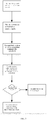
- a printer chip storage allocation method is performed through a printer main body comprising a main body operation unit and replaceable equipment provided with the printer chip and comprises the following steps of:
- the printer main body sends out the authorization request command to the printer chip, for example, 0x60 0x00 0x98 is sent, wherein 0x60 represents the chip address of the printer chip, and 0x00 0x98 represents the authorization request command;
- the second step is executed, specifically, and an authorization random number is returned, for example, 0x00 0x08 0x65 0x97 0x35 0x63 0x34 0x23 0x56 0x39 is returned, wherein 0x00 0x08 indicates the data length, and 0x65 0x97 0x35 0x63 0x34 0x23 0x56 0x39 represents the 8-bit random data;
- the third step is executed at the moment, specifically, the printer chip carries out encryption operation through the key data stored in the key unit by using the random data as input, so that the first check code is obtained, and the main body operation unit in the printer main body obtain
- the encryption operation method adopted by the printer main body and the printer chip is the AES algorithm or the DES algorithm or the EDES algorithm or the 3DES algorithm.
- the authorization request command sent by the printer main body further includes chip address data of the printer chip.
- the input data for the encryption operation method further include fixed data fixed as 00 besides the random data.
- the replaceable equipment is an ink cartridge.
- a printer chip comprises a chip control circuit, a data storage unit used for storing data, and a communication unit used for communication with a printer, wherein the data storage unit and the communication unit are electrically connected with the chip control circuit respectively;
- the printer chip is characterized in that:
- the printer chip is mounted on a replaceable component, the replaceable component is not authorized specifically in an ordinary service state, namely data on the authorization flag bit make the data storage unit in the non-authorized state, the data storage unit is divided into a plurality of areas at the moment and at least comprises the non-protected part, the protected part and the disposable part, and the three parts are different on the aspect of reading and writing permissions;
- the non-protected part allows data to be read and written therein by printing equipment such as the printer main body and is a common data operation port, data stored in the protected part are input when used for the first time, can only be read and cannot be modified or written in, for example, when the printer chip is mounted on an ink cartridge, data stored in the protected part can be the first service date of the ink cartridge, the data can only be read and cannot be modified once being written in, and a user can speculate the effective service life of the ink cartridge according to the first service date of the ink cartridge; the disposable part allows data to be written therein, however, writing can be conducted
- the disposable part When the data storage unit is in the non-authorized state, the disposable part includes the ink cartridge maximum volume data, ink cartridge protector serial number data and protection start bit data.
- the protected part includes the ink cartridge first service date.
- the operation unit carries out operation through data sent from the printer main body and the key data stored in the key unit according to the AES algorithm or the DES algorithm or the EDES algorithm or the 3DES algorithm. It has already been proved that by adoption of the AES algorithm or the DES algorithm or the EDES algorithm or the 3DES algorithm, copying and imitation are unavailable under the safe key condition, and safety of the calculation and authentication process for specific authorization is guaranteed.
- a printer chip storage allocation method is performed through a printer main body comprising a main body operation unit and replaceable equipment provided with the printer chip and comprises the following steps of:
- the printer main body sends out the authorization request command to the printer chip, for example, 0x60 0x00 0x98 is sent, wherein 0x60 represents the chip address of the printer chip, and 0x00 0x98 represents the authorization request command;
- the second step is executed, specifically, and an authorization random number is returned, for example, 0x00 0x08 0x65 0x97 0x35 0x63 0x34 0x23 0x56 0x39 is returned, wherein 0x00 0x08 indicates the data length, and 0x65 0x97 0x35 0x63 0x34 0x23 0x56 0x39 represents the 8-bit random data;
- the third step is executed at the moment, specifically, the printer chip carries out encryption operation through the key data stored in the key unit by using the random data as input, so that the first check code is obtained, and the main body operation unit in the printer main body obtain
Landscapes
- Engineering & Computer Science (AREA)
- Theoretical Computer Science (AREA)
- Computer Security & Cryptography (AREA)
- General Engineering & Computer Science (AREA)
- Computer Hardware Design (AREA)
- Physics & Mathematics (AREA)
- General Physics & Mathematics (AREA)
- Software Systems (AREA)
- Computing Systems (AREA)
- Computer Networks & Wireless Communication (AREA)
- Signal Processing (AREA)
- Ink Jet (AREA)
- Accessory Devices And Overall Control Thereof (AREA)
- Mathematical Physics (AREA)
Applications Claiming Priority (2)
| Application Number | Priority Date | Filing Date | Title |
|---|---|---|---|
| CN201510754337.6A CN105346256B (zh) | 2015-11-09 | 2015-11-09 | 一种打印机芯片、墨盒、和打印机芯片存储分配方法 |
| PCT/CN2016/096488 WO2017080281A1 (zh) | 2015-11-09 | 2016-08-24 | 一种打印机芯片、墨盒、和打印机芯片存储分配方法 |
Publications (3)
| Publication Number | Publication Date |
|---|---|
| EP3375615A1 true EP3375615A1 (de) | 2018-09-19 |
| EP3375615A4 EP3375615A4 (de) | 2018-10-03 |
| EP3375615B1 EP3375615B1 (de) | 2021-09-29 |
Family
ID=55322389
Family Applications (1)
| Application Number | Title | Priority Date | Filing Date |
|---|---|---|---|
| EP16863459.0A Active EP3375615B1 (de) | 2015-11-09 | 2016-08-24 | Druckerchip, tintenpatrone und verfahren zur zuteilung eines datenspeichers zu einem druckerchip |
Country Status (5)
| Country | Link |
|---|---|
| US (1) | US20180326735A1 (de) |
| EP (1) | EP3375615B1 (de) |
| CN (1) | CN105346256B (de) |
| ES (1) | ES2894694T3 (de) |
| WO (1) | WO2017080281A1 (de) |
Families Citing this family (22)
| Publication number | Priority date | Publication date | Assignee | Title |
|---|---|---|---|---|
| CN105346256B (zh) * | 2015-11-09 | 2017-03-22 | 杭州旗捷科技有限公司 | 一种打印机芯片、墨盒、和打印机芯片存储分配方法 |
| CN105818541B (zh) * | 2016-04-07 | 2018-10-16 | 杭州旗捷科技有限公司 | 一种墨盒芯片、墨盒及响应打印作业的操作方法 |
| GB201608285D0 (en) * | 2016-05-11 | 2016-06-22 | Videojet Technologies Inc | Printing |
| JP6814001B2 (ja) * | 2016-09-09 | 2021-01-13 | 株式会社Screenホールディングス | 印刷装置用の消耗品の使用妥当性管理システム、および、印刷装置用の消耗品の使用妥当性管理方法 |
| CN109426466A (zh) * | 2017-09-05 | 2019-03-05 | 北京立思辰计算机技术有限公司 | 一种打印机芯片及其存储分配方法 |
| CN107608905B (zh) * | 2017-09-11 | 2020-05-12 | 杭州中天微系统有限公司 | 擦写Flash数据的方法及装置 |
| CN109508157A (zh) * | 2017-09-14 | 2019-03-22 | 北京立思辰计算机技术有限公司 | 一种打印机控制器及打印机控制方法 |
| CN108116053B (zh) * | 2017-12-19 | 2019-07-26 | 杭州旗捷科技有限公司 | 一种耗材芯片认证方法、耗材芯片及成像盒 |
| CN108215513B (zh) * | 2018-02-05 | 2019-06-21 | 杭州旗捷科技有限公司 | 可变阈值的反馈电路、耗材芯片、耗材 |
| CN108382073B (zh) * | 2018-02-05 | 2019-06-21 | 杭州旗捷科技有限公司 | 可变阈值的反馈电路、耗材芯片、耗材 |
| RU2020134366A (ru) | 2018-03-21 | 2022-04-22 | Пресижн Плэнтинг Ллк | Картридж для реагентов |
| CN110395049A (zh) * | 2018-04-25 | 2019-11-01 | 广州众诺电子技术有限公司 | 高容量芯片及耗材容器 |
| CN111469560B (zh) | 2018-09-20 | 2021-07-13 | 杭州旗捷科技有限公司 | 再生墨盒 |
| CN109624529B (zh) * | 2019-01-22 | 2020-04-24 | 杭州旗捷科技有限公司 | 一种耗材芯片、耗材芯片通信方法 |
| CN109977656B (zh) | 2019-04-08 | 2019-12-20 | 广州众诺电子技术有限公司 | 身份验证方法和耗材盒及存储介质 |
| CN111614857B (zh) * | 2020-04-08 | 2022-05-13 | 广州众诺电子技术有限公司 | 芯片通信方法、耗材芯片及成像盒 |
| US12472749B2 (en) * | 2021-02-12 | 2025-11-18 | Hewlett-Packard Development Company, L.P. | Appending data on a replaceable supply component |
| CN113696627B (zh) * | 2021-08-09 | 2022-09-30 | 上海汉图科技有限公司 | 打印机 |
| CN115436842A (zh) * | 2022-09-05 | 2022-12-06 | 广州众诺电子技术有限公司 | 芯片与打印设备的连接检测方法及相关装置 |
| CN117021770A (zh) * | 2023-08-23 | 2023-11-10 | 北京微芯安信息技术有限公司 | 一种基于双安全芯片的打印机耗材鉴别方法及系统 |
| WO2026095933A1 (en) * | 2024-10-30 | 2026-05-07 | Hewlett-Packard Development Company, L.P. | Writing renewal configuration data to print component |
| WO2026095930A1 (en) * | 2024-10-30 | 2026-05-07 | Hewlett-Packard Development Company, L.P. | Fluid ejection cartridge including secure renewal status memory cell |
Family Cites Families (45)
| Publication number | Priority date | Publication date | Assignee | Title |
|---|---|---|---|---|
| US4388695A (en) * | 1980-02-21 | 1983-06-14 | Timeplex, Inc. | Hardware memory write lock circuit |
| US6702417B2 (en) * | 1997-07-12 | 2004-03-09 | Silverbrook Research Pty Ltd | Printing cartridge with capacitive sensor identification |
| US6547364B2 (en) * | 1997-07-12 | 2003-04-15 | Silverbrook Research Pty Ltd | Printing cartridge with an integrated circuit device |
| US6618117B2 (en) * | 1997-07-12 | 2003-09-09 | Silverbrook Research Pty Ltd | Image sensing apparatus including a microcontroller |
| US6803989B2 (en) * | 1997-07-15 | 2004-10-12 | Silverbrook Research Pty Ltd | Image printing apparatus including a microcontroller |
| US6158837A (en) * | 1997-09-19 | 2000-12-12 | Xerox Corporation | Printer having print mode for non-qualified marking material |
| MY125897A (en) * | 1998-11-02 | 2006-08-30 | Seiko Epson Corp | Ink cartridge and printer using the same |
| US6757832B1 (en) * | 2000-02-15 | 2004-06-29 | Silverbrook Research Pty Ltd | Unauthorized modification of values in flash memory |
| US6952778B1 (en) * | 2000-10-26 | 2005-10-04 | Cypress Semiconductor Corporation | Protecting access to microcontroller memory blocks |
| US6615329B2 (en) * | 2001-07-11 | 2003-09-02 | Intel Corporation | Memory access control system, apparatus, and method |
| US20050162455A1 (en) * | 2001-08-06 | 2005-07-28 | Kia Silverbrook | Printing cartridge with an integrated circuit device |
| US20090319802A1 (en) * | 2002-12-02 | 2009-12-24 | Silverbrook Research Pty Ltd | Key Genaration In An Integrated Circuit |
| US7182445B2 (en) * | 2003-04-25 | 2007-02-27 | Hewlett-Packard Development Company, L.P. | Replaceable printer component |
| US6982846B2 (en) * | 2003-05-19 | 2006-01-03 | International Business Machines Corporation | Tamper resistant write once recording of a data storage cartridge having rewritable media |
| DE10357429B4 (de) * | 2003-12-09 | 2018-07-19 | Heidelberger Druckmaschinen Ag | Modulare Bogenrotationsdruckmaschine |
| US7093989B2 (en) * | 2004-05-27 | 2006-08-22 | Silverbrook Research Pty Ltd | Printer comprising two uneven printhead modules and at least two printer controllers, one which spends print data to the other |
| US7266661B2 (en) * | 2004-05-27 | 2007-09-04 | Silverbrook Research Pty Ltd | Method of storing bit-pattern in plural devices |
| US7088928B2 (en) * | 2004-08-13 | 2006-08-08 | Static Control Components, Inc. | Systems and methods for universal imaging components |
| US7257335B1 (en) * | 2004-12-17 | 2007-08-14 | Nu-Kote International, Inc. | Universal smart chip cartridges for multiple printing apparatus |
| US7773237B2 (en) * | 2007-02-22 | 2010-08-10 | Kabushiki Kaisha Toshiba | Image forming apparatus, image forming method and image forming system |
| US20080304364A1 (en) * | 2007-06-08 | 2008-12-11 | Michael Holtzman | Memory device with circuitry for improving accuracy of a time estimate |
| EP2336944A1 (de) * | 2008-10-10 | 2011-06-22 | Panasonic Corporation | Informationsverarbeitungseinrichtung, authentifizierungssystem, authentifizierungseinrichtung, informationsverarbeitungsverfahren, informationsverarbeitungsprogramm, aufzeichnungsmedium und integrierte schaltung |
| JP2011230464A (ja) * | 2010-04-30 | 2011-11-17 | Seiko Epson Corp | 液体噴射装置 |
| CN201909948U (zh) * | 2010-06-02 | 2011-07-27 | 珠海赛纳打印科技股份有限公司 | 一带多成像盒芯片、成像系统及成像盒 |
| US8281983B2 (en) * | 2010-06-28 | 2012-10-09 | Xerox Corporation | Method and apparatus for storing and verifying serial numbers using smart labels in an image production device |
| CN101950342B (zh) * | 2010-09-20 | 2013-03-13 | 北京海泰方圆科技有限公司 | 一种集成电路卡访问控制权限的管理装置及方法 |
| US8682639B2 (en) * | 2010-09-21 | 2014-03-25 | Texas Instruments Incorporated | Dedicated memory window for emulation address |
| US8311419B2 (en) * | 2010-11-29 | 2012-11-13 | Xerox Corporation | Consumable ID differentiation and validation system with on-board processor |
| FR2969788B1 (fr) * | 2010-12-27 | 2013-02-08 | Electricite De France | Procede et dispositif de controle d'acces a un systeme informatique |
| CN102189810A (zh) * | 2011-04-06 | 2011-09-21 | 珠海艾派克微电子有限公司 | 验证成像盒芯片的成像装置及方法 |
| CN102231054B (zh) * | 2011-06-08 | 2013-01-02 | 珠海天威技术开发有限公司 | 芯片及芯片数据通信方法、耗材容器、成像设备 |
| EP2737392B1 (de) * | 2011-07-29 | 2021-05-26 | Hewlett-Packard Development Company, L.P. | Drucker |
| CN102442073B (zh) * | 2011-09-27 | 2013-11-27 | 珠海天威技术开发有限公司 | 通用芯片及其通信方法、耗材容器、成像设备 |
| CN202517844U (zh) * | 2012-04-06 | 2012-11-07 | 珠海天威技术开发有限公司 | 存储芯片、耗材容器、成像设备 |
| CN102831352B (zh) * | 2012-09-11 | 2015-02-18 | 南京天溯自动化控制系统有限公司 | 设备授权使用的方法及其设备 |
| US9030682B2 (en) * | 2013-01-02 | 2015-05-12 | Static Control Components, Inc. | Systems and methods for universal imaging components |
| US9104140B2 (en) * | 2013-03-15 | 2015-08-11 | Ologn Technologies Ag | Systems, methods and apparatuses for authorized use and refill of a printer cartridge |
| JP5472843B1 (ja) * | 2013-08-23 | 2014-04-16 | 利仁 曽根 | カートリッジシステム、正規品判定に利用されるicチップ |
| CN103862879B (zh) * | 2014-01-15 | 2016-08-17 | 珠海艾派克微电子有限公司 | 一种墨盒芯片及使用该芯片的墨盒 |
| JP2015168161A (ja) * | 2014-03-07 | 2015-09-28 | 理想科学工業株式会社 | インクジェット印刷装置 |
| JP6439370B2 (ja) * | 2014-05-28 | 2018-12-19 | 株式会社リコー | 情報処理システム、情報処理方法、情報処理装置及びプログラム |
| CN104765987A (zh) * | 2015-04-17 | 2015-07-08 | 深圳市西迪特科技有限公司 | 嵌入式设备软件加密的系统及方法 |
| US10114958B2 (en) * | 2015-06-16 | 2018-10-30 | Microsoft Technology Licensing, Llc | Protected regions |
| US20170126414A1 (en) * | 2015-10-28 | 2017-05-04 | Texas Instruments Incorporated | Database-less authentication with physically unclonable functions |
| CN105346256B (zh) * | 2015-11-09 | 2017-03-22 | 杭州旗捷科技有限公司 | 一种打印机芯片、墨盒、和打印机芯片存储分配方法 |
-
2015
- 2015-11-09 CN CN201510754337.6A patent/CN105346256B/zh active Active
-
2016
- 2016-08-24 EP EP16863459.0A patent/EP3375615B1/de active Active
- 2016-08-24 US US15/774,907 patent/US20180326735A1/en not_active Abandoned
- 2016-08-24 WO PCT/CN2016/096488 patent/WO2017080281A1/zh not_active Ceased
- 2016-08-24 ES ES16863459T patent/ES2894694T3/es active Active
Also Published As
| Publication number | Publication date |
|---|---|
| EP3375615A4 (de) | 2018-10-03 |
| WO2017080281A1 (zh) | 2017-05-18 |
| ES2894694T3 (es) | 2022-02-15 |
| CN105346256B (zh) | 2017-03-22 |
| CN105346256A (zh) | 2016-02-24 |
| EP3375615B1 (de) | 2021-09-29 |
| US20180326735A1 (en) | 2018-11-15 |
Similar Documents
| Publication | Publication Date | Title |
|---|---|---|
| EP3375615B1 (de) | Druckerchip, tintenpatrone und verfahren zur zuteilung eines datenspeichers zu einem druckerchip | |
| CN100354884C (zh) | 身份证制造安全 | |
| TWI505686B (zh) | 具有有限加密鑰取回的通訊系統、方法及裝置 | |
| CN104553384B (zh) | 一种耗材芯片及其序列号的识别方法和装置 | |
| CA3030129C (en) | Electronic credential management system | |
| US20110258451A1 (en) | Method for updating mobile terminal software and mobile terminal | |
| US20120284534A1 (en) | Memory Device and Method for Accessing the Same | |
| CN106295376A (zh) | 一种应用于打印领域的高效安全通信系统及其操作方法 | |
| EP2521065A2 (de) | Speichervorrichtung und Verfahren zum Zugriff darauf | |
| US20200044838A1 (en) | Data encryption method and system using device authentication key | |
| US11112725B2 (en) | Consumable chip, consumable and consumable communication method | |
| EP3096259B1 (de) | Sicherheitsramblock mit mehreren partitionen | |
| US20180232974A1 (en) | Systems and methods for authenticating a cartridge | |
| CN104281415A (zh) | 用于空调的数据处理方法和装置 | |
| CN104965738A (zh) | 机顶盒数据写入方法及系统 | |
| US20190372787A1 (en) | Communication system capable of preserving a chip-to-chip integrity | |
| CN112084468B (zh) | 一种多软件授权验证方法 | |
| US12462046B2 (en) | Electronic device and method for performing permission management of storage device | |
| JP7169193B2 (ja) | 周辺機器におけるセキュリティ保護を行なう方法および装置 | |
| CN119099210B (zh) | 打印控制方法、系统和存储介质 | |
| US20250247236A1 (en) | Logic circuitry packages storing tokens | |
| KR101659396B1 (ko) | 알에프 라이터와 알에프 리더 간 보안 처리 방법 | |
| JP2015232742A (ja) | ユーザ認証方法および射出成形機 | |
| CN110377247B (zh) | 标识处理方法、装置、计算机设备和计算机可读存储介质 | |
| KR101405007B1 (ko) | 스마트 토너 보안 시스템 |
Legal Events
| Date | Code | Title | Description |
|---|---|---|---|
| STAA | Information on the status of an ep patent application or granted ep patent |
Free format text: STATUS: THE INTERNATIONAL PUBLICATION HAS BEEN MADE |
|
| PUAI | Public reference made under article 153(3) epc to a published international application that has entered the european phase |
Free format text: ORIGINAL CODE: 0009012 |
|
| STAA | Information on the status of an ep patent application or granted ep patent |
Free format text: STATUS: REQUEST FOR EXAMINATION WAS MADE |
|
| 17P | Request for examination filed |
Effective date: 20180606 |
|
| AK | Designated contracting states |
Kind code of ref document: A1 Designated state(s): AL AT BE BG CH CY CZ DE DK EE ES FI FR GB GR HR HU IE IS IT LI LT LU LV MC MK MT NL NO PL PT RO RS SE SI SK SM TR |
|
| AX | Request for extension of the european patent |
Extension state: BA ME |
|
| A4 | Supplementary search report drawn up and despatched |
Effective date: 20180903 |
|
| RIC1 | Information provided on ipc code assigned before grant |
Ipc: H04L 29/06 20060101ALI20180828BHEP Ipc: G06F 21/78 20130101ALI20180828BHEP Ipc: G06F 12/14 20060101ALI20180828BHEP Ipc: G06F 21/44 20130101ALI20180828BHEP Ipc: B41J 2/175 20060101AFI20180828BHEP |
|
| DAV | Request for validation of the european patent (deleted) | ||
| DAX | Request for extension of the european patent (deleted) | ||
| STAA | Information on the status of an ep patent application or granted ep patent |
Free format text: STATUS: EXAMINATION IS IN PROGRESS |
|
| 17Q | First examination report despatched |
Effective date: 20190711 |
|
| GRAP | Despatch of communication of intention to grant a patent |
Free format text: ORIGINAL CODE: EPIDOSNIGR1 |
|
| STAA | Information on the status of an ep patent application or granted ep patent |
Free format text: STATUS: GRANT OF PATENT IS INTENDED |
|
| INTG | Intention to grant announced |
Effective date: 20210401 |
|
| GRAS | Grant fee paid |
Free format text: ORIGINAL CODE: EPIDOSNIGR3 |
|
| GRAA | (expected) grant |
Free format text: ORIGINAL CODE: 0009210 |
|
| STAA | Information on the status of an ep patent application or granted ep patent |
Free format text: STATUS: THE PATENT HAS BEEN GRANTED |
|
| AK | Designated contracting states |
Kind code of ref document: B1 Designated state(s): AL AT BE BG CH CY CZ DE DK EE ES FI FR GB GR HR HU IE IS IT LI LT LU LV MC MK MT NL NO PL PT RO RS SE SI SK SM TR |
|
| REG | Reference to a national code |
Ref country code: GB Ref legal event code: FG4D |
|
| REG | Reference to a national code |
Ref country code: CH Ref legal event code: EP Ref country code: AT Ref legal event code: REF Ref document number: 1433880 Country of ref document: AT Kind code of ref document: T Effective date: 20211015 |
|
| REG | Reference to a national code |
Ref country code: DE Ref legal event code: R096 Ref document number: 602016064460 Country of ref document: DE |
|
| REG | Reference to a national code |
Ref country code: IE Ref legal event code: FG4D |
|
| REG | Reference to a national code |
Ref country code: LT Ref legal event code: MG9D |
|
| PG25 | Lapsed in a contracting state [announced via postgrant information from national office to epo] |
Ref country code: HR Free format text: LAPSE BECAUSE OF FAILURE TO SUBMIT A TRANSLATION OF THE DESCRIPTION OR TO PAY THE FEE WITHIN THE PRESCRIBED TIME-LIMIT Effective date: 20210929 Ref country code: FI Free format text: LAPSE BECAUSE OF FAILURE TO SUBMIT A TRANSLATION OF THE DESCRIPTION OR TO PAY THE FEE WITHIN THE PRESCRIBED TIME-LIMIT Effective date: 20210929 Ref country code: NO Free format text: LAPSE BECAUSE OF FAILURE TO SUBMIT A TRANSLATION OF THE DESCRIPTION OR TO PAY THE FEE WITHIN THE PRESCRIBED TIME-LIMIT Effective date: 20211229 Ref country code: LT Free format text: LAPSE BECAUSE OF FAILURE TO SUBMIT A TRANSLATION OF THE DESCRIPTION OR TO PAY THE FEE WITHIN THE PRESCRIBED TIME-LIMIT Effective date: 20210929 Ref country code: BG Free format text: LAPSE BECAUSE OF FAILURE TO SUBMIT A TRANSLATION OF THE DESCRIPTION OR TO PAY THE FEE WITHIN THE PRESCRIBED TIME-LIMIT Effective date: 20211229 Ref country code: SE Free format text: LAPSE BECAUSE OF FAILURE TO SUBMIT A TRANSLATION OF THE DESCRIPTION OR TO PAY THE FEE WITHIN THE PRESCRIBED TIME-LIMIT Effective date: 20210929 Ref country code: RS Free format text: LAPSE BECAUSE OF FAILURE TO SUBMIT A TRANSLATION OF THE DESCRIPTION OR TO PAY THE FEE WITHIN THE PRESCRIBED TIME-LIMIT Effective date: 20210929 |
|
| REG | Reference to a national code |
Ref country code: NL Ref legal event code: MP Effective date: 20210929 |
|
| REG | Reference to a national code |
Ref country code: ES Ref legal event code: FG2A Ref document number: 2894694 Country of ref document: ES Kind code of ref document: T3 Effective date: 20220215 Ref country code: AT Ref legal event code: MK05 Ref document number: 1433880 Country of ref document: AT Kind code of ref document: T Effective date: 20210929 |
|
| PG25 | Lapsed in a contracting state [announced via postgrant information from national office to epo] |
Ref country code: LV Free format text: LAPSE BECAUSE OF FAILURE TO SUBMIT A TRANSLATION OF THE DESCRIPTION OR TO PAY THE FEE WITHIN THE PRESCRIBED TIME-LIMIT Effective date: 20210929 Ref country code: GR Free format text: LAPSE BECAUSE OF FAILURE TO SUBMIT A TRANSLATION OF THE DESCRIPTION OR TO PAY THE FEE WITHIN THE PRESCRIBED TIME-LIMIT Effective date: 20211230 |
|
| PG25 | Lapsed in a contracting state [announced via postgrant information from national office to epo] |
Ref country code: AT Free format text: LAPSE BECAUSE OF FAILURE TO SUBMIT A TRANSLATION OF THE DESCRIPTION OR TO PAY THE FEE WITHIN THE PRESCRIBED TIME-LIMIT Effective date: 20210929 |
|
| PG25 | Lapsed in a contracting state [announced via postgrant information from national office to epo] |
Ref country code: IS Free format text: LAPSE BECAUSE OF FAILURE TO SUBMIT A TRANSLATION OF THE DESCRIPTION OR TO PAY THE FEE WITHIN THE PRESCRIBED TIME-LIMIT Effective date: 20220129 Ref country code: SK Free format text: LAPSE BECAUSE OF FAILURE TO SUBMIT A TRANSLATION OF THE DESCRIPTION OR TO PAY THE FEE WITHIN THE PRESCRIBED TIME-LIMIT Effective date: 20210929 Ref country code: RO Free format text: LAPSE BECAUSE OF FAILURE TO SUBMIT A TRANSLATION OF THE DESCRIPTION OR TO PAY THE FEE WITHIN THE PRESCRIBED TIME-LIMIT Effective date: 20210929 Ref country code: PT Free format text: LAPSE BECAUSE OF FAILURE TO SUBMIT A TRANSLATION OF THE DESCRIPTION OR TO PAY THE FEE WITHIN THE PRESCRIBED TIME-LIMIT Effective date: 20220131 Ref country code: PL Free format text: LAPSE BECAUSE OF FAILURE TO SUBMIT A TRANSLATION OF THE DESCRIPTION OR TO PAY THE FEE WITHIN THE PRESCRIBED TIME-LIMIT Effective date: 20210929 Ref country code: NL Free format text: LAPSE BECAUSE OF FAILURE TO SUBMIT A TRANSLATION OF THE DESCRIPTION OR TO PAY THE FEE WITHIN THE PRESCRIBED TIME-LIMIT Effective date: 20210929 Ref country code: EE Free format text: LAPSE BECAUSE OF FAILURE TO SUBMIT A TRANSLATION OF THE DESCRIPTION OR TO PAY THE FEE WITHIN THE PRESCRIBED TIME-LIMIT Effective date: 20210929 Ref country code: CZ Free format text: LAPSE BECAUSE OF FAILURE TO SUBMIT A TRANSLATION OF THE DESCRIPTION OR TO PAY THE FEE WITHIN THE PRESCRIBED TIME-LIMIT Effective date: 20210929 Ref country code: AL Free format text: LAPSE BECAUSE OF FAILURE TO SUBMIT A TRANSLATION OF THE DESCRIPTION OR TO PAY THE FEE WITHIN THE PRESCRIBED TIME-LIMIT Effective date: 20210929 |
|
| REG | Reference to a national code |
Ref country code: DE Ref legal event code: R097 Ref document number: 602016064460 Country of ref document: DE |
|
| PG25 | Lapsed in a contracting state [announced via postgrant information from national office to epo] |
Ref country code: DK Free format text: LAPSE BECAUSE OF FAILURE TO SUBMIT A TRANSLATION OF THE DESCRIPTION OR TO PAY THE FEE WITHIN THE PRESCRIBED TIME-LIMIT Effective date: 20210929 |
|
| PLBE | No opposition filed within time limit |
Free format text: ORIGINAL CODE: 0009261 |
|
| STAA | Information on the status of an ep patent application or granted ep patent |
Free format text: STATUS: NO OPPOSITION FILED WITHIN TIME LIMIT |
|
| 26N | No opposition filed |
Effective date: 20220630 |
|
| PG25 | Lapsed in a contracting state [announced via postgrant information from national office to epo] |
Ref country code: SI Free format text: LAPSE BECAUSE OF FAILURE TO SUBMIT A TRANSLATION OF THE DESCRIPTION OR TO PAY THE FEE WITHIN THE PRESCRIBED TIME-LIMIT Effective date: 20210929 |
|
| PG25 | Lapsed in a contracting state [announced via postgrant information from national office to epo] |
Ref country code: MC Free format text: LAPSE BECAUSE OF FAILURE TO SUBMIT A TRANSLATION OF THE DESCRIPTION OR TO PAY THE FEE WITHIN THE PRESCRIBED TIME-LIMIT Effective date: 20210929 |
|
| PG25 | Lapsed in a contracting state [announced via postgrant information from national office to epo] |
Ref country code: LU Free format text: LAPSE BECAUSE OF NON-PAYMENT OF DUE FEES Effective date: 20220824 |
|
| REG | Reference to a national code |
Ref country code: BE Ref legal event code: MM Effective date: 20220831 |
|
| PG25 | Lapsed in a contracting state [announced via postgrant information from national office to epo] |
Ref country code: IE Free format text: LAPSE BECAUSE OF NON-PAYMENT OF DUE FEES Effective date: 20220824 |
|
| PG25 | Lapsed in a contracting state [announced via postgrant information from national office to epo] |
Ref country code: BE Free format text: LAPSE BECAUSE OF NON-PAYMENT OF DUE FEES Effective date: 20220831 |
|
| PGFP | Annual fee paid to national office [announced via postgrant information from national office to epo] |
Ref country code: IT Payment date: 20230809 Year of fee payment: 8 Ref country code: CH Payment date: 20230902 Year of fee payment: 8 |
|
| PG25 | Lapsed in a contracting state [announced via postgrant information from national office to epo] |
Ref country code: HU Free format text: LAPSE BECAUSE OF FAILURE TO SUBMIT A TRANSLATION OF THE DESCRIPTION OR TO PAY THE FEE WITHIN THE PRESCRIBED TIME-LIMIT; INVALID AB INITIO Effective date: 20160824 |
|
| PG25 | Lapsed in a contracting state [announced via postgrant information from national office to epo] |
Ref country code: SM Free format text: LAPSE BECAUSE OF FAILURE TO SUBMIT A TRANSLATION OF THE DESCRIPTION OR TO PAY THE FEE WITHIN THE PRESCRIBED TIME-LIMIT Effective date: 20210929 Ref country code: CY Free format text: LAPSE BECAUSE OF FAILURE TO SUBMIT A TRANSLATION OF THE DESCRIPTION OR TO PAY THE FEE WITHIN THE PRESCRIBED TIME-LIMIT Effective date: 20210929 |
|
| PG25 | Lapsed in a contracting state [announced via postgrant information from national office to epo] |
Ref country code: MK Free format text: LAPSE BECAUSE OF FAILURE TO SUBMIT A TRANSLATION OF THE DESCRIPTION OR TO PAY THE FEE WITHIN THE PRESCRIBED TIME-LIMIT Effective date: 20210929 |
|
| PG25 | Lapsed in a contracting state [announced via postgrant information from national office to epo] |
Ref country code: TR Free format text: LAPSE BECAUSE OF FAILURE TO SUBMIT A TRANSLATION OF THE DESCRIPTION OR TO PAY THE FEE WITHIN THE PRESCRIBED TIME-LIMIT Effective date: 20210929 |
|
| PG25 | Lapsed in a contracting state [announced via postgrant information from national office to epo] |
Ref country code: MT Free format text: LAPSE BECAUSE OF FAILURE TO SUBMIT A TRANSLATION OF THE DESCRIPTION OR TO PAY THE FEE WITHIN THE PRESCRIBED TIME-LIMIT Effective date: 20210929 |
|
| REG | Reference to a national code |
Ref country code: CH Ref legal event code: PL |
|
| PG25 | Lapsed in a contracting state [announced via postgrant information from national office to epo] |
Ref country code: CH Free format text: LAPSE BECAUSE OF NON-PAYMENT OF DUE FEES Effective date: 20240831 |
|
| PG25 | Lapsed in a contracting state [announced via postgrant information from national office to epo] |
Ref country code: IT Free format text: LAPSE BECAUSE OF NON-PAYMENT OF DUE FEES Effective date: 20240824 |
|
| PGFP | Annual fee paid to national office [announced via postgrant information from national office to epo] |
Ref country code: ES Payment date: 20250908 Year of fee payment: 10 |
|
| PGFP | Annual fee paid to national office [announced via postgrant information from national office to epo] |
Ref country code: DE Payment date: 20250812 Year of fee payment: 10 |
|
| PGFP | Annual fee paid to national office [announced via postgrant information from national office to epo] |
Ref country code: GB Payment date: 20250826 Year of fee payment: 10 |
|
| PGFP | Annual fee paid to national office [announced via postgrant information from national office to epo] |
Ref country code: FR Payment date: 20250828 Year of fee payment: 10 |