EP3372573A1 - Ceramic-aluminum conjugate, power module substrate, and power module - Google Patents
Ceramic-aluminum conjugate, power module substrate, and power module Download PDFInfo
- Publication number
- EP3372573A1 EP3372573A1 EP16861830.4A EP16861830A EP3372573A1 EP 3372573 A1 EP3372573 A1 EP 3372573A1 EP 16861830 A EP16861830 A EP 16861830A EP 3372573 A1 EP3372573 A1 EP 3372573A1
- Authority
- EP
- European Patent Office
- Prior art keywords
- amount
- aluminum
- ceramic
- power module
- bonded
- Prior art date
- Legal status (The legal status is an assumption and is not a legal conclusion. Google has not performed a legal analysis and makes no representation as to the accuracy of the status listed.)
- Granted
Links
Images



Classifications
-
- H—ELECTRICITY
- H10—SEMICONDUCTOR DEVICES; ELECTRIC SOLID-STATE DEVICES NOT OTHERWISE PROVIDED FOR
- H10W—GENERIC PACKAGES, INTERCONNECTIONS, CONNECTORS OR OTHER CONSTRUCTIONAL DETAILS OF DEVICES COVERED BY CLASS H10
- H10W70/00—Package substrates; Interposers; Redistribution layers [RDL]
- H10W70/60—Insulating or insulated package substrates; Interposers; Redistribution layers
- H10W70/67—Insulating or insulated package substrates; Interposers; Redistribution layers characterised by their insulating layers or insulating parts
- H10W70/69—Insulating materials thereof
- H10W70/692—Ceramics or glasses
-
- C—CHEMISTRY; METALLURGY
- C04—CEMENTS; CONCRETE; ARTIFICIAL STONE; CERAMICS; REFRACTORIES
- C04B—LIME, MAGNESIA; SLAG; CEMENTS; COMPOSITIONS THEREOF, e.g. MORTARS, CONCRETE OR LIKE BUILDING MATERIALS; ARTIFICIAL STONE; CERAMICS; REFRACTORIES; TREATMENT OF NATURAL STONE
- C04B37/00—Joining burned ceramic articles with other burned ceramic articles or other articles by heating
- C04B37/02—Joining burned ceramic articles with other burned ceramic articles or other articles by heating with metallic articles
- C04B37/021—Joining burned ceramic articles with other burned ceramic articles or other articles by heating with metallic articles in a direct manner, e.g. direct copper bonding [DCB]
-
- C—CHEMISTRY; METALLURGY
- C04—CEMENTS; CONCRETE; ARTIFICIAL STONE; CERAMICS; REFRACTORIES
- C04B—LIME, MAGNESIA; SLAG; CEMENTS; COMPOSITIONS THEREOF, e.g. MORTARS, CONCRETE OR LIKE BUILDING MATERIALS; ARTIFICIAL STONE; CERAMICS; REFRACTORIES; TREATMENT OF NATURAL STONE
- C04B37/00—Joining burned ceramic articles with other burned ceramic articles or other articles by heating
- C04B37/02—Joining burned ceramic articles with other burned ceramic articles or other articles by heating with metallic articles
- C04B37/023—Joining burned ceramic articles with other burned ceramic articles or other articles by heating with metallic articles characterised by the interlayer used
- C04B37/025—Joining burned ceramic articles with other burned ceramic articles or other articles by heating with metallic articles characterised by the interlayer used consisting of glass or ceramic material
-
- B—PERFORMING OPERATIONS; TRANSPORTING
- B23—MACHINE TOOLS; METAL-WORKING NOT OTHERWISE PROVIDED FOR
- B23K—SOLDERING OR UNSOLDERING; WELDING; CLADDING OR PLATING BY SOLDERING OR WELDING; CUTTING BY APPLYING HEAT LOCALLY, e.g. FLAME CUTTING; WORKING BY LASER BEAM
- B23K1/00—Soldering, e.g. brazing, or unsoldering
- B23K1/0008—Soldering, e.g. brazing, or unsoldering specially adapted for particular articles or work
- B23K1/0016—Soldering of electronic components
-
- B—PERFORMING OPERATIONS; TRANSPORTING
- B23—MACHINE TOOLS; METAL-WORKING NOT OTHERWISE PROVIDED FOR
- B23K—SOLDERING OR UNSOLDERING; WELDING; CLADDING OR PLATING BY SOLDERING OR WELDING; CUTTING BY APPLYING HEAT LOCALLY, e.g. FLAME CUTTING; WORKING BY LASER BEAM
- B23K35/00—Rods, electrodes, materials, or media, for use in soldering, welding, or cutting
- B23K35/02—Rods, electrodes, materials, or media, for use in soldering, welding, or cutting characterised by mechanical features, e.g. shape
- B23K35/0222—Rods, electrodes, materials, or media, for use in soldering, welding, or cutting characterised by mechanical features, e.g. shape for use in soldering or brazing
- B23K35/0233—Sheets or foils
- B23K35/0238—Sheets or foils layered
-
- B—PERFORMING OPERATIONS; TRANSPORTING
- B23—MACHINE TOOLS; METAL-WORKING NOT OTHERWISE PROVIDED FOR
- B23K—SOLDERING OR UNSOLDERING; WELDING; CLADDING OR PLATING BY SOLDERING OR WELDING; CUTTING BY APPLYING HEAT LOCALLY, e.g. FLAME CUTTING; WORKING BY LASER BEAM
- B23K35/00—Rods, electrodes, materials, or media, for use in soldering, welding, or cutting
- B23K35/22—Rods, electrodes, materials, or media, for use in soldering, welding, or cutting characterised by the composition or nature of the material
- B23K35/24—Selection of soldering or welding materials proper
- B23K35/28—Selection of soldering or welding materials proper with the principal constituent melting at less than 950°C
- B23K35/286—Al as the principal constituent
-
- C—CHEMISTRY; METALLURGY
- C04—CEMENTS; CONCRETE; ARTIFICIAL STONE; CERAMICS; REFRACTORIES
- C04B—LIME, MAGNESIA; SLAG; CEMENTS; COMPOSITIONS THEREOF, e.g. MORTARS, CONCRETE OR LIKE BUILDING MATERIALS; ARTIFICIAL STONE; CERAMICS; REFRACTORIES; TREATMENT OF NATURAL STONE
- C04B37/00—Joining burned ceramic articles with other burned ceramic articles or other articles by heating
- C04B37/02—Joining burned ceramic articles with other burned ceramic articles or other articles by heating with metallic articles
-
- H—ELECTRICITY
- H10—SEMICONDUCTOR DEVICES; ELECTRIC SOLID-STATE DEVICES NOT OTHERWISE PROVIDED FOR
- H10W—GENERIC PACKAGES, INTERCONNECTIONS, CONNECTORS OR OTHER CONSTRUCTIONAL DETAILS OF DEVICES COVERED BY CLASS H10
- H10W40/00—Arrangements for thermal protection or thermal control
- H10W40/10—Arrangements for heating
-
- H—ELECTRICITY
- H10—SEMICONDUCTOR DEVICES; ELECTRIC SOLID-STATE DEVICES NOT OTHERWISE PROVIDED FOR
- H10W—GENERIC PACKAGES, INTERCONNECTIONS, CONNECTORS OR OTHER CONSTRUCTIONAL DETAILS OF DEVICES COVERED BY CLASS H10
- H10W40/00—Arrangements for thermal protection or thermal control
- H10W40/20—Arrangements for cooling
- H10W40/25—Arrangements for cooling characterised by their materials
- H10W40/255—Arrangements for cooling characterised by their materials having a laminate or multilayered structure, e.g. direct bond copper [DBC] ceramic substrates
-
- H—ELECTRICITY
- H10—SEMICONDUCTOR DEVICES; ELECTRIC SOLID-STATE DEVICES NOT OTHERWISE PROVIDED FOR
- H10W—GENERIC PACKAGES, INTERCONNECTIONS, CONNECTORS OR OTHER CONSTRUCTIONAL DETAILS OF DEVICES COVERED BY CLASS H10
- H10W70/00—Package substrates; Interposers; Redistribution layers [RDL]
- H10W70/60—Insulating or insulated package substrates; Interposers; Redistribution layers
-
- H—ELECTRICITY
- H10—SEMICONDUCTOR DEVICES; ELECTRIC SOLID-STATE DEVICES NOT OTHERWISE PROVIDED FOR
- H10W—GENERIC PACKAGES, INTERCONNECTIONS, CONNECTORS OR OTHER CONSTRUCTIONAL DETAILS OF DEVICES COVERED BY CLASS H10
- H10W70/00—Package substrates; Interposers; Redistribution layers [RDL]
- H10W70/60—Insulating or insulated package substrates; Interposers; Redistribution layers
- H10W70/67—Insulating or insulated package substrates; Interposers; Redistribution layers characterised by their insulating layers or insulating parts
- H10W70/69—Insulating materials thereof
-
- C—CHEMISTRY; METALLURGY
- C04—CEMENTS; CONCRETE; ARTIFICIAL STONE; CERAMICS; REFRACTORIES
- C04B—LIME, MAGNESIA; SLAG; CEMENTS; COMPOSITIONS THEREOF, e.g. MORTARS, CONCRETE OR LIKE BUILDING MATERIALS; ARTIFICIAL STONE; CERAMICS; REFRACTORIES; TREATMENT OF NATURAL STONE
- C04B2237/00—Aspects relating to ceramic laminates or to joining of ceramic articles with other articles by heating
- C04B2237/30—Composition of layers of ceramic laminates or of ceramic or metallic articles to be joined by heating, e.g. Si substrates
- C04B2237/32—Ceramic
- C04B2237/36—Non-oxidic
- C04B2237/366—Aluminium nitride
-
- C—CHEMISTRY; METALLURGY
- C04—CEMENTS; CONCRETE; ARTIFICIAL STONE; CERAMICS; REFRACTORIES
- C04B—LIME, MAGNESIA; SLAG; CEMENTS; COMPOSITIONS THEREOF, e.g. MORTARS, CONCRETE OR LIKE BUILDING MATERIALS; ARTIFICIAL STONE; CERAMICS; REFRACTORIES; TREATMENT OF NATURAL STONE
- C04B2237/00—Aspects relating to ceramic laminates or to joining of ceramic articles with other articles by heating
- C04B2237/30—Composition of layers of ceramic laminates or of ceramic or metallic articles to be joined by heating, e.g. Si substrates
- C04B2237/40—Metallic
- C04B2237/402—Aluminium
-
- H—ELECTRICITY
- H10—SEMICONDUCTOR DEVICES; ELECTRIC SOLID-STATE DEVICES NOT OTHERWISE PROVIDED FOR
- H10W—GENERIC PACKAGES, INTERCONNECTIONS, CONNECTORS OR OTHER CONSTRUCTIONAL DETAILS OF DEVICES COVERED BY CLASS H10
- H10W90/00—Package configurations
- H10W90/701—Package configurations characterised by the relative positions of pads or connectors relative to package parts
- H10W90/731—Package configurations characterised by the relative positions of pads or connectors relative to package parts of die-attach connectors
- H10W90/734—Package configurations characterised by the relative positions of pads or connectors relative to package parts of die-attach connectors between a chip and a stacked insulating package substrate, interposer or RDL
Definitions
- the present invention relates to a ceramic-aluminum bonded body obtained by bonding a ceramic member made of AlN and an aluminum member, a power module substrate including a ceramic substrate made of AlN and an aluminum plate bonded to the ceramic substrate, and a power module including the power module substrate.
- a structure in which semiconductor element is bonded onto a circuit layer made of a conductive material is provided.
- a heating value is large. Therefore, as a substrate on which the power semiconductor element is mounted, for example, a power module substrate including a ceramic substrate made of AlN (aluminum nitride), Al 2 O 3 (alumina), and the like, and a circuit layer which is formed by bonding a metal sheet excellent in conductivity to one face of the ceramic substrate have been widely used from the related art.
- a substrate in which a metal layer is formed by bonding a metal sheet to the other face of the ceramic substrate is also provided.
- a power module substrate in which an aluminum plate serving as a circuit layer is bonded to one face of the ceramic substrate made of AlN (aluminum nitride) via an Al-Si-based brazing material and an aluminum plate serving as a metal layer is bonded to the other face of the ceramic substrate via an Al-Si-based brazing material, has been proposed.
- a semiconductor element as a power element is mounted on the circuit layer via a solder layer to be used as a power module.
- a copper heat sink may be bonded to a metal layer side via solder.
- a bonding property between the ceramic substrate and the aluminum plate is improved by removing an oxide which inhibits bonding by unevenly distributed Mg.
- the bonding property is improved by unevenly distributing Mg to a bonded interface between the brazing material and the aluminum plate or a bonded interface between the brazing material and the ceramic substrate.
- unevenly distributing Mg the bonding between the ceramic substrate and the aluminum plate is rather inhibited and the bonding reliability may deteriorate.
- aluminum in the vicinity of the bonded interface is hardened by the segregated Mg, and there is a possibility that a crack occurs in the ceramic substrate at the time of temperature cycle load.
- the present invention has been made in view of the above-described circumstances, and an object thereof is to provide a ceramic-aluminum bonded body, a power module substrate, and a power module including the power module substrate, in each of which the ceramic member and the aluminum member are reliably bonded to each other, and which are excellent in bonding reliability at the time of temperature cycle load and capable of suppressing the occurrence of cracking in the ceramic member.
- the ceramic-aluminum bonded body includes: a ceramic member made of AlN; and an aluminum member, the ceramic member and the aluminum member being bonded together, wherein Mg-containing oxides having a spinel crystal structure are dispersed in the aluminum member within a range of 2 ⁇ m in a thickness direction from a bonded interface with the ceramic member, a segregated portion in which Mg, Si, and O are segregated is formed in the aluminum member in the vicinity of the bonded interface with the ceramic member, ratios of an amount of Mg[Mg] S , an amount of Si[Si] S , and an amount of O[O] S in the segregated portion to an amount of Mg[Mg] I , an amount of Si[Si] I , and an amount of O[O] I , respectively, at a position spaced by 10 ⁇ m from the bonded
- the Mg-containing oxide having a spinel crystal structure is dispersed in the aluminum member within the range of 2 ⁇ m in a thickness direction from a bonded interface with the ceramic member.
- the Mg-containing oxide having a spinel crystal structure is formed by reaction between an oxide film formed on a surface of the aluminum member and Mg.
- the oxide film formed on the surface of the aluminum member is sufficiently removed by reaction with the Mg. Accordingly, it becomes possible to reliably bond the aluminum member and the ceramic member to each other.
- the segregated portion in which Mg, Si, and O are segregated is included, the ratios of the amount of Mg [Mg]s, the amount of Si[Si] S , and the amount of O[O] S in the segregated portion to the amount of Mg[Mg] I , the amount of Si[Si] I , and the amount of O[O] I , respectively, at the position spaced by 10 ⁇ m from the bonded interface toward the aluminum member side are within the ranges of 1 ⁇ [Mg] S /[Mg] I ⁇ 15, 1 ⁇ [Si] S /[Si] I ⁇ 25, and 1 ⁇ [O] S /[O] I ⁇ 25, and Mg, Si, and O are segregated in the aluminum member in the vicinity of the bonded interface with the ceramic member.
- the aluminum member itself can be prevented from hardening and deformation resistance of the aluminum member can be prevented from increasing.
- an amount of Cu is 1.2 mass% or less, and an amount of Fe be 0.6 mass% or less.
- the amount of Cu is limited to 1.2 mass% or less and the amount of Fe is limited to 0.6 mass% or less, the vicinity of the bonded interface of the aluminum member with the ceramic member can be prevented from excessively hardening and cracking or the like can be prevented from occurring in the ceramic member.
- the power module substrate includes: a ceramic substrate made of AlN; and an aluminum plate bonded to the ceramic substrate, wherein Mg-containing oxides having a spinel crystal structure are dispersed in the aluminum plate within a range of 2 ⁇ m in a thickness direction from a bonded interface with the ceramic substrate, a segregated portion in which Mg, Si, and O are segregated is in an area of the aluminum plate in the vicinity of the bonded interface with the ceramic substrate, ratios of an amount of Mg[Mg] S , an amount of Si[Si] S , and an amount of O[O] S in the segregated portion respectively to an amount of Mg[Mg] I , an amount of Si[Si] I , and an amount of O[O] I at a position spaced by 10 ⁇ m from the bonded interface toward an aluminum plate side are respectively within ranges of 1 ⁇ [Mg] S /[Mg] I ⁇ 15, 1 ⁇ [Mg] S /[Mg] I ⁇ 15, 1 ⁇
- the Mg-containing oxides having the spinel crystal structure are dispersed in the aluminum plate within the range of 2 ⁇ m in the thickness direction from the bonded interface with the ceramic substrate. Therefore, the oxide film formed on the surface of the aluminum plate is sufficiently removed by reaction with the Mg, and it becomes possible to reliably bond the aluminum plate and the ceramic substrate to each other.
- the Mg, Si, and O are segregated in the aluminum plate in the vicinity of the bonded interface with the ceramic substrate, it is possible to stabilize interfacial energy and improve bonding reliability between the aluminum plate and the ceramic substrate.
- the vicinity of the bonded interface of the aluminum plate with the ceramic substrate can be prevented from excessively hardening.
- the amount of Mg[Mg] I at the position spaced by 10 ⁇ m from the bonded interface toward the aluminum plate side is 0.8 mass% or less, the deformation resistance of the aluminum plate can be prevented from increasing.
- an amount of Cu is 1.2 mass% or less, and an amount of Fe be 0.6 mass% or less.
- the amount of Cu is limited to 1.2 mass% or less and the amount of Fe is limited to 0.6 mass% or less, the vicinity of the bonded interface of the aluminum plate with the ceramic substrate can be prevented from excessively hardening.
- cracking or the like can be prevented from occurring in the ceramic substrate.
- a power module including: the power module substrate described above; and a semiconductor element.
- the ceramic substrate and the aluminum plate are firmly bonded to each other, which is particularly excellent in reliability.
- the present invention it is possible to provide a ceramic-aluminum bonded body, a power module substrate, and a power module including the power module substrate, in each of which the ceramic member and the aluminum member are reliably bonded to each other, and which are excellent in bonding reliability at the time of temperature cycle load and capable of suppressing the occurrence of cracking in the ceramic member.
- a ceramic-aluminum bonded body is a power module substrate 10 including a ceramic substrate 11 as a ceramic member made of AlN, a circuit layer 12 to which an aluminum plate 22 is bonded as an aluminum member, and a metal layer 13 to which an aluminum plate 23 is bonded.
- FIG. 1 shows a power module 1 using the power module substrate 10 according to the embodiment of the present invention.
- the power module 1 includes the power module substrate 10 in which the circuit layer 12 and the metal layer 13 are disposed on the ceramic substrate 11, a semiconductor element 3 which is bonded to one face (an upper face in Fig. 1 ) of the circuit layer 12 via a first solder layer 2, and a heat sink 40 which is bonded to the other face (a lower face in Fig. 1 ) of the metal layer 13 via a second solder layer 4.
- the first solder layer 2 and the second solder layer 4 are, for example, made of Sn-Ag-based solder material, Sn-ln-based solder material or Sn-Ag-Cu-based solder material.
- a Ni-plated layer (not shown) is provided between the circuit layer 12 and the first solder layer 2, and between the metal layer 13 and the second solder layer 4.
- the power module substrate 10 includes the ceramic substrate 11, the circuit layer 12 which is disposed on one face (an upper face in Fig. 1 ) of the ceramic substrate 11, and the metal layer 13 which is disposed on the other face (a lower face in Fig. 1 ) of the ceramic substrate 11.
- the ceramic substrate 11 prevents the circuit layer 12 and the metal layer 13 from being electrically connected therebetween.
- the ceramic substrate 11 is made of AlN (aluminum nitride) having high insulation.
- a thickness of the ceramic substrate 11 is set within a range of 0.2 to 1.5 mm, and in the present embodiment, is set to 0.635 mm.
- the circuit layer 12 is formed by bonding the metal sheet having conductivity to one face of the ceramic substrate 11.
- the circuit layer 12 is formed by bonding the aluminum plate 22 made of an aluminum (called 4N aluminum) rolled sheet having a purity of 99.99 mass% or higher to the ceramic substrate 11.
- a circuit pattern is formed, and one face (an upper face in Fig. 1 ) of the circuit layer 12 serves as a mounting face on which the semiconductor element 3 is mounted.
- a thickness of the circuit layer 12 (aluminum plate 22) is set within a range of 0.05 mm or more and less than 1.1 mm, and in the present embodiment, is set to 0.6 mm.
- the metal layer 13 is formed by bonding the metal sheet which is excellent in thermal conductivity to the other face of the ceramic substrate 11.
- the metal layer 13 is formed by bonding the aluminum plate 23 made of an aluminum (called 4N aluminum) rolled sheet having a purity of 99.99 mass% or higher to the ceramic substrate 11.
- a thickness of the metal layer 13 (aluminum plate 23) is set within a range of 0.05 mm or more and less than 3.0 mm, and in the present embodiment, is set to 0.6 mm.
- the heat sink 40 is to cool the power module substrate 10 described above, and includes a radiator plate 41 bonded to the power module substrate 10 and a cooler 42 which is disposed on the radiator plate 41 in a laminated manner.
- the radiator plate 41 diffuses heat from the power module substrate 10 described above in a surface direction, and in the present embodiment, is made of a copper plate which is excellent in thermal conductivity.
- the cooler 42 includes a flow path 43 for circulating a cooling medium (for example, cooling water).
- a cooling medium for example, cooling water.
- the cooler 42 is desirably made of a material which has good thermal conductivity, and in the present embodiment, is made of A6063 (aluminum alloy).
- the radiator plate 41 and the cooler 42 are fastened by a fixing screw 45.
- Mg-containing oxides 36 having a spinel crystal structure are dispersed in the circuit layer 12 or the metal layer 13 within a range of 2 ⁇ m in a thickness direction from a bonded interface 30 with the ceramic substrate 11.
- the Mg-containing oxide 36 can be confirmed by the following method.
- an electron diffraction pattern is obtained using a transmission electron microscope (TEM) (Titan ChemiSTEM manufactured by FEI Company, an acceleration voltage of 200 kV) to analyze a composition using an energy-dispersive X-ray spectroscopy (EDS) (NSS7 manufactured by Thermo Fisher Scientific Inc.).
- TEM transmission electron microscope
- EDS energy-dispersive X-ray spectroscopy
- the electron diffraction pattern is obtained by performing irradiation with an electron beam narrowed down to approximately 1 nm (nanobeam diffraction (NBD) method).
- NBD nanobeam diffraction
- the Mg-containing oxide 36 contains Mg and Al.
- An area ratio of the Mg-containing oxide 36 within a range of 2 ⁇ m in a thickness direction from the bonded interface 30 is in a range of 2% or higher and 18% or lower. It is preferable that 90% or more of observed Mg-containing oxide 36 be present within a range of 1 ⁇ m in the thickness direction from the bonded interface 30.
- a segregated portion 31 in which Mg, Si, and O are segregated is formed in the vicinity of the bonded interface 30 of the circuit layer 12 or the metal layer 13 with the ceramic substrate 11.
- the segregated portion 31 may be within a range of 0.01 ⁇ m in the thickness direction from the bonded interface 30 of the circuit layer 12 and the metal layer 13 with the ceramic substrate 11, but is not limited thereto.
- the ratios are not limited thereto.
- the amount of Mg [Mg] S in the segregated portion 31 is set in a range of 0.1 mass% or more and 1.5 mass% or less, and the amount of Si[Si] S is in a range of 0.1 mass% or more and 2.5 mass% or less, and the amount of O[O] S is set to 1.5 mass% or more and 15 mass% or less.
- the amount of Mg[Mg] S , the amount of Si[Si] S , and the amount of O[O] S in the segregated portion 31 are obtained by performing a TEM analysis on a part of the bonded interface 30 containing the segregated portion 31, with a beam diameter of 1 nm.
- an amount of Cu in the segregated portion 31 is 1.2 mass% or less and an amount of Fe is 0.6 mass% or less.
- the amount of Cu in the segregated portion 31 is preferably 0.00 mass% or more and 0.05 mass% or less and the amount of Fe is preferably 0.00 mass% or more and 0.05 mass% or less, but is not limited thereto.
- the aluminum plates 22 and 23 and the ceramic substrate 11 are bonded to each other to form the circuit layer 12 and the metal layer 13.
- a circuit layer and metal layer-forming step S01 includes a laminating step S11, a heating step S12, and a molten metal-solidifying step S13.
- the aluminum plate 22 is laminated on one face of the ceramic substrate 11 via an Al-Si-Mg-based brazing material 24 and the aluminum plate 23 is laminated on the other face of the ceramic substrate 11 via an Al-Si-Mg-based brazing material 25, thereby forming a laminate.
- brazing material foil made of aluminum alloy containing Si in a range of 1 mass% or more and 12 mass% or less and Mg in a range of 0.01 mass% or more and 0.05 mass% or less is used, and each thickness of the brazing materials 24 and 25 is in a range of 5 ⁇ m or more and 30 ⁇ m or less.
- the laminate described above is charged into a heating furnace 29 in a state of being pressed in a laminating direction to be heated. Then, some of the brazing materials 24 and 25 and the aluminum plates 22 and 23 are melted and molten metal areas are formed respectively in interfaces between the aluminum plates 22 and 23 and the ceramic substrate 11.
- Conditions of the heating step S12 are set such that an atmosphere is a vacuum atmosphere (10 -4 Pa or higher and 10 -3 Pa or lower) or a nitrogen atmosphere in which an oxygen tension is 500 volppm or lower, a bonding temperature is in a range of 580°C or higher and 650°C or lower, and a heating time is in a range of 1 minute or longer and 180 minutes or shorter.
- the pressing device 50 includes a base plate 51, guide posts 52 vertically attached to four corners of an upper surface of the base plate 51, a fixing plate 53 disposed at upper end portions of the guide posts 52, a pressing plate 54 which is movable up and down freely between the base plate 51 and the fixing plate 53 and supported by a guide post 52, an urging means 55 such as a spring which is provided between the fixing plate 53 and the pressing plate 54 and is for urging the pressing plate 54 downward, and an adjusting screw 56 for moving the fixing plate 53 up and down.
- the fixing plate 53 and the pressing plate 54 are disposed in parallel with the base plate 51.
- the laminate described above is disposed between the base plate 51 and the pressing plate 54 via a carbon sheet 57.
- the pressing device 50 has a structure in which the fixing plate 53 is caused to move up and down by adjusting a position of the adjusting screw 56 and the pressing plate 54 is pushed by urging means 55, thereby pressing the laminate.
- a thermal expansion coefficient of the guide post 52 is set to be greater than a thermal expansion coefficient of the urging means 55.
- the pressing load in the bonding temperature described above is in a range of 0.01 kgf/cm 2 or more and less than 1.0 kgf/cm 2 (0.98 kPa or more and less than 98 kPa).
- the pressing load in the bonding temperature described above is in a range of 0.01 kgf/cm 2 or more and less than 1.0 kgf/cm 2 (0.98 kPa or more and less than 98 kPa).
- the pressing load in the bonding temperature described above is preferably 0.05 kgf/cm 2 or more and less than 0.9 kgf/cm 2 , but is not limited thereto.
- molten metal areas respectively formed in the interfaces between the aluminum plates 22 and 23 and the ceramic substrate 11 are solidified to bond the ceramic substrate 11 to the aluminum plate 22 and aluminum plate 23.
- the power module substrate 10 is manufactured in which the circuit layer 12 and the metal layer 13 are formed on the ceramic substrate 11.
- the radiator plate 41 is bonded to the other face (a face on the opposite side to the ceramic substrate 11) of the metal layer 13 of the power module substrate 10 via the second solder layer 4 and the radiator plate 41 is fastened to the cooler 42 by the fixing screw 45. Accordingly, the heat sink 40 and the power module substrate 10 are bonded to each other.
- the semiconductor element 3 is mounted to one face (a face on the opposite side to the ceramic substrate 11) of the circuit layer 12 via the first solder layer 2. Accordingly, the power module 1 according to the present embodiment is produced.
- the Mg-containing oxides 36 having a spinel crystal structure are dispersed in the circuit layer 12 or the metal layer 13 within the range of 2 ⁇ m in the thickness direction from the bonded interface 30 with the ceramic substrate 11, the oxide films formed on the surfaces of the aluminum plates 22 and 23 serving as the circuit layer 12 and the metal layer 13 are sufficiently removed by reaction with the Mg, and it becomes possible to reliably bond the circuit layer 12 to the ceramic substrate 11, and the metal layer 13 to the ceramic substrate 11.
- the oxide films formed on the surfaces of the aluminum plates 22 and 23 serving as the circuit layer 12 and the metal layer 13 can be reliably removed, and it becomes possible to reliably bond the circuit layer 12 to the ceramic substrate 11, and the metal layer 13 to the ceramic substrate 11.
- the area ratio of the Mg-containing oxide 36 within a range of 2 ⁇ m in the thickness direction from the bonded interface 30 is 18% or lower, the Mg-containing oxide 36 is not excessively present and cracking or the like in the vicinity of the bonded interface 30 can be prevented from occurring.
- the segregated portion 31 in which Mg, Si, and O are segregated is included in the vicinity of the bonded interface 30 of the circuit layer 12 and the metal layer 13, to which the aluminum plates 22 and 23 are bonded respectively, with the ceramic substrate 11.
- the vicinity of the bonded interfaces 30 of the circuit layer 12 and the metal layer 13 with the ceramic substrate 11 can be prevented from excessively hardening.
- cracking or the like can be prevented from occurring in the ceramic substrate 11.
- the circuit layer 12 and the metal layer 13 themselves can be prevented from hardening and cracking or the like can be prevented from occurring in the ceramic substrate 11.
- the amount of Cu is limited to 1.2 mass% or less and the amount of Fe is limited to 0.6 mass% or less, the vicinity of the bonded interfaces 30 of the circuit layer 12 and the metal layer 13 with the ceramic substrate 11 can be prevented from excessively hardening and cracking or the like can be prevented from occurring in the ceramic substrate 11.
- the pressing load in a predetermined bonding temperature is in a range of 0.01 kgf/cm 2 or more and less than 1 kgf/cm 2 (0.98 kPa or more and less than 98 kPa)
- an interfacial reaction does not excessively occur and Mg is prevented from being excessively segregated in the vicinity of the bonded interface 30, thereby making it possible to segregate an appropriate amount of Mg.
- the power module substrate is described as an example, but the present invention is not limited thereto, as long as it is a ceramic-aluminum bonded body formed by bonding the ceramic member made of AlN and the aluminum member to each other.
- each of the circuit layer and the metal layer is formed by bonding an aluminum (4N aluminum) rolled sheet having a purity of 99.99 mass% or higher, but the present invention is not limited thereto, as long as at least one of the circuit layer and the metal layer is made of pure aluminum such as aluminum (2N aluminum) having a purity of 99 mass% or higher or aluminum (3N aluminum) having a purity of 99.9 mass% or higher or aluminum alloy such as A3003 (Si: 0.6 mass% or less, Fe: 0.7 mass% or less, Cu: 0.05 mass% or more and 0.20 mass% or less, Mn: 1.0 mass% or more and 1.5 mass% or less, Zn: 0.10 mass% or less, and Al: balance).
- the circuit layer may be made of a copper plate made of copper or a copper alloy, a laminated plate of aluminum and copper, or the like.
- the metal layer may be made of a copper plate made of copper or a copper alloy, a laminated plate of aluminum and copper, or the like, and may be set as a structure not forming the metal layer.
- a base layer may be formed by other means such as Ag paste.
- the heat sink is not limited to the example in the present embodiment, and there is no particular limitation in a structure of the heat sink.
- a rolled sheet (37 mm ⁇ 37 mm) having the composition and the thickness shown in Table 1 was prepared.
- a substrate (40 mm ⁇ 40 mm) having the composition and the thickness shown in Table 1 was prepared.
- an aluminum (4N aluminum) rolled sheet (37 mmx37 mmxthickness 1.6 mm) having a purity of 99.99 mass% or higher was prepared.
- the aluminum plate forming the circuit layer and the aluminum plate forming the metal layer were laminated to the ceramic substrate via the brazing material (thickness 20 ⁇ m) shown in Table 1, and brazed under the conditions shown in Table 1.
- the power module substrate for an evaluation was manufactured.
- a composition ([Mg] S , [Si] S , [O] S , Cu, and Fe) of the segregated layer and a composition ([Mg] I , [Si] I , and [O] I ) in the circuit layer were measured by the following method.
- the obtained power module substrate was mechanically cut in the laminating direction.
- the obtained cross section was mechanically polished to a thickness of approximately 50 ⁇ m to obtain a cross section sample.
- 4 kV argon ions were caused to be implanted to the vicinity of the bonded interface from up and down sides (face perpendicular to the laminating direction) at an angle of 4 degrees, and the cross section sample was flacked by sputtering until a hole was bored. Since an edge of the hole becomes an edge shape and the thickness at which the electron beam can pass is approximately 0.1 ⁇ m, the portion was measured with a TEM and an EDS and the composition of the segregated layer was measured.
- the measurement of the TEM and the EDS was performed using the Titan ChemiSTEM (manufactured by FEI Company, with an EDS detector) under the acceleration voltage of 200 kV and a beam diameter of 1 nm, at a magnification of one million times.
- composition in the circuit layer a composition at a position spaced by 10 ⁇ m from the bonded interface toward the aluminum plate side was taken as the composition in the circuit layer.
- an electron diffraction pattern was obtained using a transmission electron microscope (Titan ChemiSTEM manufactured by FEI Company, an acceleration voltage of 200 kV) to analyze a composition using an energy-dispersive X-ray spectroscopy (NSS7 manufactured by Thermo Fisher Scientific Inc.).
- the electron diffraction pattern was obtained by performing irradiation with an electron beam narrowed down to approximately 1 nm (NBD method).
- mapping of N and Mg was performed using the transmission electron microscope (Titan ChemiSTEM manufactured by FEI Company) at a magnification of 10000 times within a range of 2 ⁇ m in the thickness direction from the bonded interface between the ceramic substrate and the metal layer.
- a boundary between an area in which N was detected and an area in which N was not detected was set as the bonded interface.
- An area in which a concentration of Mg was 6 to 12 at% from the mapping of Mg was set as Mg-containing oxide.
- Binarization was performed. Then the area ratio of the Mg-containing oxide was obtained by dividing the area of the Mg-containing oxide by the measurement area. The measurement was performed at five places, and the average value thereof was taken as the area ratio.
- the area ratios of the Mg-containing oxide having the spinel crystal structure within a range of 2 ⁇ m in the thickness direction from the bonded interface are shown in Table 3.
- the heat sink was bonded to the other face of the metal layer of the power module substrate described above.
- the heat sink was 50 mm ⁇ 60 mm ⁇ 5 mmt of A3003 alloy aluminum plate.
- bonding was performed using Al-Si brazing foil by heating at 610°C in vacuum in a state of being pressed at 3.0 kgf/cm 2 (0.29 MPa).
- a temperature cycle test was carried out using the heat sink-attached power module substrate obtained in this manner.
- TSB-51 manufactured by ESPEC CORP.
- One cycle was set for 5 minutes at -40°C and 5 minutes at 150°C and 2000 cycles of test were carried out on the heat sink-attached power module substrate in a liquid phase (Fluorinert). Then, the bonding rate between the circuit layer and the ceramic substrate was evaluated as described below. An evaluation of the bonding rate was performed before the temperature cycle test (initial bonding rate) and after the temperature cycle test (bonding rate after cycles).
- the bonding rate of the interface between the ceramic substrate and the metal layer was evaluated using an ultrasonic flaw detection device (FineSAT200 manufactured by Hitachi Power Solutions Co.,Ltd.) and the bonding rate was calculated from the following formula. The evaluation results are shown in Table 3.
- the initial bonding area was set to an area to be bonded before the bonding, that is, an area (37 mmx37 mm) of the metal layer in the present example.
- Bonding Rate Initial Area to be Bonded ⁇ Peeled Area / Initial Area to be Bonded ⁇ 100
- the temperature cycle test was carried out using the heat sink-attached power module substrate described above. The measurement conditions are shown below. After 2000 cycles, the presence or absence of cracking in the ceramic substrate was confirmed using the ultrasonic flaw detection device. The evaluation results are shown in Table 3.
- Comparative Example 8 in which Al 2 O 3 was used for the ceramic substrate [Mg] S /[Mg] I was out of the range of the present invention and the bonding rate after the temperature cycle test was lowered.
- the present invention it is possible to provide a ceramic-aluminum bonded body, a power module substrate, and a power module including the power module substrate, in each of which the ceramic member and the aluminum member are reliably bonded to each other, and which are excellent in bonding reliability at the time of temperature cycle load and capable of suppressing the occurrence of cracking in the ceramic member.
Landscapes
- Engineering & Computer Science (AREA)
- Chemical & Material Sciences (AREA)
- Ceramic Engineering (AREA)
- Mechanical Engineering (AREA)
- Materials Engineering (AREA)
- Structural Engineering (AREA)
- Organic Chemistry (AREA)
- Cooling Or The Like Of Semiconductors Or Solid State Devices (AREA)
- Ceramic Products (AREA)
Abstract
Description
- The present invention relates to a ceramic-aluminum bonded body obtained by bonding a ceramic member made of AlN and an aluminum member, a power module substrate including a ceramic substrate made of AlN and an aluminum plate bonded to the ceramic substrate, and a power module including the power module substrate.
- Priority is claimed on Japanese Patent Application No.
2015-218892 filed on November 6, 2015 - In a semiconductor device such as an LED and a power module, a structure in which semiconductor element is bonded onto a circuit layer made of a conductive material is provided.
- In a power semiconductor element for high-power control used for controlling wind power generation, an electric vehicle, a hybrid vehicle, and the like, a heating value is large. Therefore, as a substrate on which the power semiconductor element is mounted, for example, a power module substrate including a ceramic substrate made of AlN (aluminum nitride), Al2O3 (alumina), and the like, and a circuit layer which is formed by bonding a metal sheet excellent in conductivity to one face of the ceramic substrate have been widely used from the related art. As the power module substrate, a substrate in which a metal layer is formed by bonding a metal sheet to the other face of the ceramic substrate is also provided.
- For example, in PTL 1, a power module substrate, in which an aluminum plate serving as a circuit layer is bonded to one face of the ceramic substrate made of AlN (aluminum nitride) via an Al-Si-based brazing material and an aluminum plate serving as a metal layer is bonded to the other face of the ceramic substrate via an Al-Si-based brazing material, has been proposed.
- In such a power module substrate, a semiconductor element as a power element is mounted on the circuit layer via a solder layer to be used as a power module. In addition, a copper heat sink may be bonded to a metal layer side via solder.
- In addition, in
PTLs 2 to 5, a ceramic circuit board, in which a ceramic substrate and an aluminum plate are bonded to each other using a brazing material containing Mg, and Mg or the like is unevenly distributed in a bonded interface between the brazing material and the aluminum plate or a bonded interface between the brazing material and the ceramic substrate, has been proposed. - In these ceramic circuit boards, a bonding property between the ceramic substrate and the aluminum plate is improved by removing an oxide which inhibits bonding by unevenly distributed Mg.
-
- [PTL 1] Republished Japanese Translation No.
WO2003/090277 of the PCT International Publication for Patent Applications - [PTL 2] Japanese Unexamined Patent Application, First Publication No.
2001-044345 - [PTL 3] Japanese Unexamined Patent Application, First Publication No.
2001-062588 - [PTL4] Japanese Unexamined Patent Application, First Publication No.
2001-102703 - [PTL 5] Japanese Unexamined Patent Application, First Publication No.
2001-144433 - In recent years, miniaturization and metal sheet thinning of the power module advance and usage environment thereof becomes more severe. Particularly, at the time of temperature cycle load, since a large shear force acts on the bonded interface between the aluminum plate and the ceramic substrate, it is further required to improve bonding reliability.
- In
PTLs 2 to 5, the bonding property is improved by unevenly distributing Mg to a bonded interface between the brazing material and the aluminum plate or a bonded interface between the brazing material and the ceramic substrate. However, in a case of merely unevenly distributing Mg, the bonding between the ceramic substrate and the aluminum plate is rather inhibited and the bonding reliability may deteriorate. In addition, aluminum in the vicinity of the bonded interface is hardened by the segregated Mg, and there is a possibility that a crack occurs in the ceramic substrate at the time of temperature cycle load. - The present invention has been made in view of the above-described circumstances, and an object thereof is to provide a ceramic-aluminum bonded body, a power module substrate, and a power module including the power module substrate, in each of which the ceramic member and the aluminum member are reliably bonded to each other, and which are excellent in bonding reliability at the time of temperature cycle load and capable of suppressing the occurrence of cracking in the ceramic member.
- In order to solve such a problem so as to achieve the object described above, a ceramic-aluminum bonded body of an aspect of the present invention is provided. The ceramic-aluminum bonded body includes: a ceramic member made of AlN; and an aluminum member, the ceramic member and the aluminum member being bonded together, wherein Mg-containing oxides having a spinel crystal structure are dispersed in the aluminum member within a range of 2 µm in a thickness direction from a bonded interface with the ceramic member, a segregated portion in which Mg, Si, and O are segregated is formed in the aluminum member in the vicinity of the bonded interface with the ceramic member, ratios of an amount of Mg[Mg]S, an amount of Si[Si]S, and an amount of O[O]S in the segregated portion to an amount of Mg[Mg]I, an amount of Si[Si]I, and an amount of O[O]I, respectively, at a position spaced by 10 µm from the bonded interface toward an aluminum member side are within ranges of 1<[Mg]S/[Mg]I≤15, 1<[Si]S/[Si]I≤25, and 1<[O]S/[O]I≤25, and the amount of Mg[Mg]I at the position spaced by 10 µm from the bonded interface toward the aluminum member side is 0.8 mass% or less.
- In the ceramic-aluminum bonded body having such a configuration, the Mg-containing oxide having a spinel crystal structure is dispersed in the aluminum member within the range of 2 µm in a thickness direction from a bonded interface with the ceramic member. Here, the Mg-containing oxide having a spinel crystal structure is formed by reaction between an oxide film formed on a surface of the aluminum member and Mg. In a case where the Mg-containing oxide having a spinel crystal structure is dispersed, the oxide film formed on the surface of the aluminum member is sufficiently removed by reaction with the Mg. Accordingly, it becomes possible to reliably bond the aluminum member and the ceramic member to each other.
- In addition, in the ceramic-aluminum bonded body, the segregated portion in which Mg, Si, and O are segregated is included, the ratios of the amount of Mg [Mg]s, the amount of Si[Si]S, and the amount of O[O]S in the segregated portion to the amount of Mg[Mg]I, the amount of Si[Si]I, and the amount of O[O]I, respectively, at the position spaced by 10 µm from the bonded interface toward the aluminum member side are within the ranges of 1<[Mg]S/[Mg]I≤15, 1<[Si]S/[Si]I≤25, and 1<[O]S/[O]I≤25, and Mg, Si, and O are segregated in the aluminum member in the vicinity of the bonded interface with the ceramic member. Accordingly, it is possible to stabilize interfacial energy and improve bonding reliability between the aluminum member and the ceramic member. In addition, since an amount of Mg, Si, and O segregated is suppressed, the vicinity of the bonded interface of the aluminum member with the ceramic member can be prevented from excessively hardening and cracking or the like can be prevented from occurring in the ceramic member.
- Further, since the amount of Mg[Mg]I at the position spaced by 10 µm from the bonded interface toward the aluminum member side is 0.8 mass% or less, the aluminum member itself can be prevented from hardening and deformation resistance of the aluminum member can be prevented from increasing.
- Here, in the ceramic-aluminum bonded body according to the aspect of the present invention, it is preferable that, in the segregated portion, an amount of Cu is 1.2 mass% or less, and an amount of Fe be 0.6 mass% or less.
- In this case, since in the segregated portion, the amount of Cu is limited to 1.2 mass% or less and the amount of Fe is limited to 0.6 mass% or less, the vicinity of the bonded interface of the aluminum member with the ceramic member can be prevented from excessively hardening and cracking or the like can be prevented from occurring in the ceramic member.
- In addition, a power module substrate of another aspect of the present invention is provided. The power module substrate includes: a ceramic substrate made of AlN; and an aluminum plate bonded to the ceramic substrate, wherein Mg-containing oxides having a spinel crystal structure are dispersed in the aluminum plate within a range of 2 µm in a thickness direction from a bonded interface with the ceramic substrate, a segregated portion in which Mg, Si, and O are segregated is in an area of the aluminum plate in the vicinity of the bonded interface with the ceramic substrate, ratios of an amount of Mg[Mg]S, an amount of Si[Si]S, and an amount of O[O]S in the segregated portion respectively to an amount of Mg[Mg]I, an amount of Si[Si]I, and an amount of O[O]I at a position spaced by 10 µm from the bonded interface toward an aluminum plate side are respectively within ranges of 1<[Mg]S/[Mg]I≤15, 1<[Si]S/[Si]I≤25, and 1<[O]S/[O]I≤25, and the amount of Mg[Mg]I at the position spaced by 10 µm from the bonded interface toward the aluminum plate side is 0.8 mass% or less.
- In the power module substrate having such a configuration, the Mg-containing oxides having the spinel crystal structure are dispersed in the aluminum plate within the range of 2 µm in the thickness direction from the bonded interface with the ceramic substrate. Therefore, the oxide film formed on the surface of the aluminum plate is sufficiently removed by reaction with the Mg, and it becomes possible to reliably bond the aluminum plate and the ceramic substrate to each other.
- In addition, in the power module substrate described above, since the Mg, Si, and O are segregated in the aluminum plate in the vicinity of the bonded interface with the ceramic substrate, it is possible to stabilize interfacial energy and improve bonding reliability between the aluminum plate and the ceramic substrate. In addition, the vicinity of the bonded interface of the aluminum plate with the ceramic substrate can be prevented from excessively hardening. When the temperature cycle is loaded on the power module substrate, cracking or the like can be prevented from occurring in the ceramic substrate.
- Further, when the amount of Mg[Mg]I at the position spaced by 10 µm from the bonded interface toward the aluminum plate side is 0.8 mass% or less, the deformation resistance of the aluminum plate can be prevented from increasing.
- Here, in the power module substrate according to the aspect of the present invention, it is preferable that, in the segregated portion, an amount of Cu is 1.2 mass% or less, and an amount of Fe be 0.6 mass% or less.
- In this case, since in the segregated portion, the amount of Cu is limited to 1.2 mass% or less and the amount of Fe is limited to 0.6 mass% or less, the vicinity of the bonded interface of the aluminum plate with the ceramic substrate can be prevented from excessively hardening. When the temperature cycle is loaded on the power module substrate, cracking or the like can be prevented from occurring in the ceramic substrate.
- According to still another aspect of the present invention, a power module is provided, including: the power module substrate described above; and a semiconductor element.
- In the power module having such a configuration, since the power module substrate is included, the ceramic substrate and the aluminum plate are firmly bonded to each other, which is particularly excellent in reliability.
- According to the present invention, it is possible to provide a ceramic-aluminum bonded body, a power module substrate, and a power module including the power module substrate, in each of which the ceramic member and the aluminum member are reliably bonded to each other, and which are excellent in bonding reliability at the time of temperature cycle load and capable of suppressing the occurrence of cracking in the ceramic member.
-
-
FIG. 1 is a schematic explanatory diagram of a power module using a power module substrate according to an embodiment of the present invention. -
FIG. 2 is a schematic explanatory diagram of the vicinity of a bonded interface between a ceramic substrate and an aluminum plate (a circuit layer and a metal layer) of the power module substrate according to the embodiment of the present invention. -
FIG. 3 is a flowchart showing a method of manufacturing the power module substrate according to the embodiment of the present invention. -
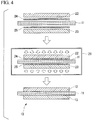
FIG. 4 is an explanatory diagram showing the method of manufacturing the power module substrate according to the embodiment of the present invention. -
FIG. 5 is an explanatory diagram of a pressing device used in the method of manufacturing the power module substrate according to the embodiment of the present invention. - Hereinafter, an embodiment of the present invention will be described with reference to the attached drawings. A ceramic-aluminum bonded body according to the embodiment is a
power module substrate 10 including aceramic substrate 11 as a ceramic member made of AlN, acircuit layer 12 to which analuminum plate 22 is bonded as an aluminum member, and ametal layer 13 to which analuminum plate 23 is bonded. -
FIG. 1 shows a power module 1 using thepower module substrate 10 according to the embodiment of the present invention. - The power module 1 includes the
power module substrate 10 in which thecircuit layer 12 and themetal layer 13 are disposed on theceramic substrate 11, asemiconductor element 3 which is bonded to one face (an upper face inFig. 1 ) of thecircuit layer 12 via afirst solder layer 2, and aheat sink 40 which is bonded to the other face (a lower face inFig. 1 ) of themetal layer 13 via asecond solder layer 4. - Here, the
first solder layer 2 and thesecond solder layer 4 are, for example, made of Sn-Ag-based solder material, Sn-ln-based solder material or Sn-Ag-Cu-based solder material. In the present embodiment, a Ni-plated layer (not shown) is provided between thecircuit layer 12 and thefirst solder layer 2, and between themetal layer 13 and thesecond solder layer 4. - The
power module substrate 10 includes theceramic substrate 11, thecircuit layer 12 which is disposed on one face (an upper face inFig. 1 ) of theceramic substrate 11, and themetal layer 13 which is disposed on the other face (a lower face inFig. 1 ) of theceramic substrate 11. - The
ceramic substrate 11 prevents thecircuit layer 12 and themetal layer 13 from being electrically connected therebetween. In the present embodiment, theceramic substrate 11 is made of AlN (aluminum nitride) having high insulation. In addition, a thickness of theceramic substrate 11 is set within a range of 0.2 to 1.5 mm, and in the present embodiment, is set to 0.635 mm. - The
circuit layer 12 is formed by bonding the metal sheet having conductivity to one face of theceramic substrate 11. In the present embodiment, as shown inFig. 4 , thecircuit layer 12 is formed by bonding thealuminum plate 22 made of an aluminum (called 4N aluminum) rolled sheet having a purity of 99.99 mass% or higher to theceramic substrate 11. In thecircuit layer 12, a circuit pattern is formed, and one face (an upper face inFig. 1 ) of thecircuit layer 12 serves as a mounting face on which thesemiconductor element 3 is mounted. Here, a thickness of the circuit layer 12 (aluminum plate 22) is set within a range of 0.05 mm or more and less than 1.1 mm, and in the present embodiment, is set to 0.6 mm. - The
metal layer 13 is formed by bonding the metal sheet which is excellent in thermal conductivity to the other face of theceramic substrate 11. In the present embodiment, as shown inFig. 4 , themetal layer 13 is formed by bonding thealuminum plate 23 made of an aluminum (called 4N aluminum) rolled sheet having a purity of 99.99 mass% or higher to theceramic substrate 11. Here, a thickness of the metal layer 13 (aluminum plate 23) is set within a range of 0.05 mm or more and less than 3.0 mm, and in the present embodiment, is set to 0.6 mm. - The
heat sink 40 is to cool thepower module substrate 10 described above, and includes aradiator plate 41 bonded to thepower module substrate 10 and a cooler 42 which is disposed on theradiator plate 41 in a laminated manner. - The
radiator plate 41 diffuses heat from thepower module substrate 10 described above in a surface direction, and in the present embodiment, is made of a copper plate which is excellent in thermal conductivity. - As shown in
Fig. 1 , the cooler 42 includes aflow path 43 for circulating a cooling medium (for example, cooling water). The cooler 42 is desirably made of a material which has good thermal conductivity, and in the present embodiment, is made of A6063 (aluminum alloy). - As shown in
Fig. 1 , theradiator plate 41 and the cooler 42 are fastened by a fixingscrew 45. - In the present embodiment, as shown in
Fig. 2 , Mg-containingoxides 36 having a spinel crystal structure are dispersed in thecircuit layer 12 or themetal layer 13 within a range of 2 µm in a thickness direction from a bondedinterface 30 with theceramic substrate 11. - The Mg-containing
oxide 36 can be confirmed by the following method. - With respect to the bonded interface, an electron diffraction pattern is obtained using a transmission electron microscope (TEM) (Titan ChemiSTEM manufactured by FEI Company, an acceleration voltage of 200 kV) to analyze a composition using an energy-dispersive X-ray spectroscopy (EDS) (NSS7 manufactured by Thermo Fisher Scientific Inc.). An area which was identified as a spinel structure from the electron diffraction pattern and an area in which the composition was Mg=6 to 12 at%, O=30 to 60 at%, and Al=balance were set as Mg-containing
oxide 36. The electron diffraction pattern is obtained by performing irradiation with an electron beam narrowed down to approximately 1 nm (nanobeam diffraction (NBD) method). - The Mg-containing
oxide 36 contains Mg and Al. An area ratio of the Mg-containingoxide 36 within a range of 2 µm in a thickness direction from the bondedinterface 30 is in a range of 2% or higher and 18% or lower. It is preferable that 90% or more of observed Mg-containingoxide 36 be present within a range of 1 µm in the thickness direction from the bondedinterface 30. - In addition, in the present embodiment, as shown in
Fig. 2 , asegregated portion 31 in which Mg, Si, and O are segregated is formed in the vicinity of the bondedinterface 30 of thecircuit layer 12 or themetal layer 13 with theceramic substrate 11. Thesegregated portion 31 may be within a range of 0.01 µm in the thickness direction from the bondedinterface 30 of thecircuit layer 12 and themetal layer 13 with theceramic substrate 11, but is not limited thereto. - Here, ratios of an amount of Mg[Mg]S, an amount of Si[Si]S, and an amount of O[O]S in the
segregated portion 31 to an amount of Mg[Mg]I, an amount of Si[Si]I, and an amount of O[O]I, respectively, at a position spaced by H=10 µm from the bondedinterface 30 toward acircuit layer 12 side or ametal layer 13 side are within ranges of 1<[Mg]S/[Mg]I≤15, 1<[Si]S/[Si]I≤25, and 1<[O]S/[O]I≤25. The ratios of the amount of Mg [Mg]s, the amount of Si [Si]s, and the amount of O [O]s in thesegregated portion 31 to the amount of Mg[Mg]I, the amount of Si[Si]I, and the amount of O[O]I, respectively, at the position spaced by H=10 µm from the bondedinterface 30 toward thecircuit layer 12 side or themetal layer 13 side are preferably 1.14<[Mg]S/[Mg]I≤12.67, 1.16<[Si]S/[Si]I≤12.67, and 1.45<[O]S/[O]I≤11.73, and more preferably 1.52<[Mg]S/[Mg]I≤5.50, 2.31<[Si]S/[Si]I≤8.35, and 1.93<[O]S/[O]I≤7.64. However, the ratios are not limited thereto. - The amount of Mg [Mg]S in the
segregated portion 31 is set in a range of 0.1 mass% or more and 1.5 mass% or less, and the amount of Si[Si]S is in a range of 0.1 mass% or more and 2.5 mass% or less, and the amount of O[O]S is set to 1.5 mass% or more and 15 mass% or less. - As shown in
Fig. 2 , the amount of Mg[Mg]S, the amount of Si[Si]S, and the amount of O[O]S in thesegregated portion 31 are obtained by performing a TEM analysis on a part of the bondedinterface 30 containing thesegregated portion 31, with a beam diameter of 1 nm. Similarly, the amount of Mg[Mg]I, the amount of Si[Si]I, and the amount of O[O]I at the position spaced by H=10 µm from the bondedinterface 30 toward thecircuit layer 12 side or themetal layer 13 side are also obtained by performing the TEM analysis with a beam diameter of 1 nm. - In addition, in the present embodiment, the amount of Mg[Mg]I at the position spaced by H=10 µm from the bonded
interface 30 toward thecircuit layer 12 side or themetal layer 13 side is 0.8 mass% or less. The amount of Mg[Mg]I at the position spaced by H=10 µm from the bondedinterface 30 toward thecircuit layer 12 side or themetal layer 13 side is preferably 0.1 mass% or more and 0.5 mass% or less, but is not limited thereto. - Further, in the present embodiment, an amount of Cu in the
segregated portion 31 is 1.2 mass% or less and an amount of Fe is 0.6 mass% or less. The amount of Cu in thesegregated portion 31 is preferably 0.00 mass% or more and 0.05 mass% or less and the amount of Fe is preferably 0.00 mass% or more and 0.05 mass% or less, but is not limited thereto. - Next, a method of manufacturing the
power module substrate 10 according to the embodiment described above will be described with reference toFigs. 3 and4 . - First, the
aluminum plates ceramic substrate 11 are bonded to each other to form thecircuit layer 12 and themetal layer 13. - In the present embodiment, as shown in
Fig. 3 , a circuit layer and metal layer-forming step S01 includes a laminating step S11, a heating step S12, and a molten metal-solidifying step S13. - In the laminating step S11, as shown in
Fig. 4 , thealuminum plate 22 is laminated on one face of theceramic substrate 11 via an Al-Si-Mg-basedbrazing material 24 and thealuminum plate 23 is laminated on the other face of theceramic substrate 11 via an Al-Si-Mg-basedbrazing material 25, thereby forming a laminate. - Here, in the present embodiment, as the Al-Si-Mg-based
brazing materials brazing materials - In the heating step S12, the laminate described above is charged into a
heating furnace 29 in a state of being pressed in a laminating direction to be heated. Then, some of thebrazing materials aluminum plates aluminum plates ceramic substrate 11. Conditions of the heating step S12 are set such that an atmosphere is a vacuum atmosphere (10-4 Pa or higher and 10-3Pa or lower) or a nitrogen atmosphere in which an oxygen tension is 500 volppm or lower, a bonding temperature is in a range of 580°C or higher and 650°C or lower, and a heating time is in a range of 1 minute or longer and 180 minutes or shorter. - Here, in the present embodiment, the laminate described above is pressed in the laminating direction using a
pressing device 50 shown inFig. 5 . Thepressing device 50 includes abase plate 51, guide posts 52 vertically attached to four corners of an upper surface of thebase plate 51, a fixingplate 53 disposed at upper end portions of the guide posts 52, apressing plate 54 which is movable up and down freely between thebase plate 51 and the fixingplate 53 and supported by aguide post 52, an urging means 55 such as a spring which is provided between the fixingplate 53 and thepressing plate 54 and is for urging thepressing plate 54 downward, and an adjustingscrew 56 for moving the fixingplate 53 up and down. - The fixing
plate 53 and thepressing plate 54 are disposed in parallel with thebase plate 51. The laminate described above is disposed between thebase plate 51 and thepressing plate 54 via acarbon sheet 57. - Therefore, the
pressing device 50 has a structure in which the fixingplate 53 is caused to move up and down by adjusting a position of the adjustingscrew 56 and thepressing plate 54 is pushed by urgingmeans 55, thereby pressing the laminate. - In the
pressing device 50, a thermal expansion coefficient of theguide post 52 is set to be greater than a thermal expansion coefficient of the urging means 55. When heating is performed up to the bonding temperature in a state of being pressed at room temperature, there is a possibility that a pressing load is lowered. - Accordingly, in the heating step S12 using the
pressing device 50, the pressing load in the bonding temperature described above is in a range of 0.01 kgf/cm2 or more and less than 1.0 kgf/cm2 (0.98 kPa or more and less than 98 kPa). - Here, in a case where the pressing load in the bonding temperature described above is less than 0.01 kgf/cm2 (0.98 kPa), there is a possibility that warping of the
ceramic substrate 11 cannot be corrected. In addition, there is a possibility that at the time of forming the molten metal area, positional deviation of thealuminum plates - From the above description, in the present embodiment, the pressing load in the bonding temperature described above is in a range of 0.01 kgf/cm2 or more and less than 1.0 kgf/cm2 (0.98 kPa or more and less than 98 kPa). The pressing load in the bonding temperature described above is preferably 0.05 kgf/cm2 or more and less than 0.9 kgf/cm2, but is not limited thereto.
- In the molten metal-solidifying step S13, molten metal areas respectively formed in the interfaces between the
aluminum plates ceramic substrate 11 are solidified to bond theceramic substrate 11 to thealuminum plate 22 andaluminum plate 23. - Accordingly, the
power module substrate 10 is manufactured in which thecircuit layer 12 and themetal layer 13 are formed on theceramic substrate 11. - Next, the
radiator plate 41 is bonded to the other face (a face on the opposite side to the ceramic substrate 11) of themetal layer 13 of thepower module substrate 10 via thesecond solder layer 4 and theradiator plate 41 is fastened to the cooler 42 by the fixingscrew 45. Accordingly, theheat sink 40 and thepower module substrate 10 are bonded to each other. - In addition, the
semiconductor element 3 is mounted to one face (a face on the opposite side to the ceramic substrate 11) of thecircuit layer 12 via thefirst solder layer 2. Accordingly, the power module 1 according to the present embodiment is produced. - In the
power module substrate 10 according to the present embodiment configured as described above, since the Mg-containingoxides 36 having a spinel crystal structure are dispersed in thecircuit layer 12 or themetal layer 13 within the range of 2 µm in the thickness direction from the bondedinterface 30 with theceramic substrate 11, the oxide films formed on the surfaces of thealuminum plates circuit layer 12 and themetal layer 13 are sufficiently removed by reaction with the Mg, and it becomes possible to reliably bond thecircuit layer 12 to theceramic substrate 11, and themetal layer 13 to theceramic substrate 11. - Here, in the present embodiment, since the area ratio of the Mg-containing
oxide 36 within a range of 2 µm in the thickness direction from the bondedinterface 30 is 2% or higher, the oxide films formed on the surfaces of thealuminum plates circuit layer 12 and themetal layer 13 can be reliably removed, and it becomes possible to reliably bond thecircuit layer 12 to theceramic substrate 11, and themetal layer 13 to theceramic substrate 11. - Further, since the area ratio of the Mg-containing
oxide 36 within a range of 2 µm in the thickness direction from the bondedinterface 30 is 18% or lower, the Mg-containingoxide 36 is not excessively present and cracking or the like in the vicinity of the bondedinterface 30 can be prevented from occurring. - In addition, in the
power module substrate 10 according to the present embodiment, thesegregated portion 31 in which Mg, Si, and O are segregated is included in the vicinity of the bondedinterface 30 of thecircuit layer 12 and themetal layer 13, to which thealuminum plates ceramic substrate 11. The ratios of the amount of Mg[Mg]S, the amount of Si[Si]S, and the amount of O [O]S in thesegregated portion 31 to the amount of Mg[Mg]I, the amount of Si[Si]I, and the amount of O[O]I, respectively, at the position spaced by H=10 µm from the bondedinterface 30 toward thecircuit layer 12 side or themetal layer 13 side are within ranges of 1<[Mg]S/[Mg]I≤15, 1<[Si]S/[Si]I≤25, and 1<[O]S/[O]I≤25. Therefore, it is possible to stabilize interfacial energy and improve bonding reliability of thecircuit layer 12 and themetal layer 13 to theceramic substrate 11. - In addition, the vicinity of the bonded
interfaces 30 of thecircuit layer 12 and themetal layer 13 with theceramic substrate 11 can be prevented from excessively hardening. When the temperature cycle is loaded on thepower module substrate 10, cracking or the like can be prevented from occurring in theceramic substrate 11. - Here, in a case where [Mg]S/[Mg]I is 1 or lower, [Si]S/[Si]I is 1 or lower, and [O]S/[O]I is 1 or lower, there is a possibility that bonding reliability of the
circuit layer 12 and themetal layer 13 to theceramic substrate 11 cannot be sufficiently improved. On the other hand, in a case where [Mg]S/[Mg]I exceeds 15, [Si]S/[Si]I exceeds 25, and [O]S/[O]I exceeds 25, there is a possibility that crack occurs in theceramic substrate 11. - Accordingly, in the present embodiment, the ratios of the amount of Mg[Mg]S, the amount of Si[Si]S, and the amount of O[O]S in the
segregated portion 31 to the amount of Mg[Mg]I, the amount of Si[Si]I, and the amount of O[O]I, respectively, at the position spaced by H=10 µm from the bondedinterface 30 toward thecircuit layer 12 side or themetal layer 13 side are within ranges of 1<[Mg]S/[Mg]I≤15, 1<[Si]S/[Si]I≤25, and 1<[O]S/[O]I≤25. - Further, since the amount of Mg[Mg]I at the position spaced by H=10 µm from the bonded
interface 30 toward thecircuit layer 12 side or themetal layer 13 side is 0.8 mass% or less, thecircuit layer 12 and themetal layer 13 themselves can be prevented from hardening and cracking or the like can be prevented from occurring in theceramic substrate 11. - Particularly, in the present embodiment, since in the
segregated portion 31, the amount of Cu is limited to 1.2 mass% or less and the amount of Fe is limited to 0.6 mass% or less, the vicinity of the bondedinterfaces 30 of thecircuit layer 12 and themetal layer 13 with theceramic substrate 11 can be prevented from excessively hardening and cracking or the like can be prevented from occurring in theceramic substrate 11. - In addition, in the present embodiment, since in the heating step S12, the pressing load in a predetermined bonding temperature is in a range of 0.01 kgf/cm2 or more and less than 1 kgf/cm2 (0.98 kPa or more and less than 98 kPa), an interfacial reaction does not excessively occur and Mg is prevented from being excessively segregated in the vicinity of the bonded
interface 30, thereby making it possible to segregate an appropriate amount of Mg. Accordingly, it is possible to manufacture thepower module substrate 10 in which the ratios of the amount of Mg[Mg]S, the amount of Si[Si]S, and the amount of O[O]S in thesegregated portion 31 to the amount of Mg [Mg]I, the amount of Si[Si]I, respectively, and the amount of O[O]I at the position spaced by H=10 µm from the bondedinterface 30 toward thecircuit layer 12 side or themetal layer 13 side are respectively within ranges of 1<[Mg]S/[Mg]I≤15, 1<[Si]S/[Si]I≤25, and 1<[O]S/[O]I≤25. - Hereinabove, the embodiment of the present invention is described. However, the present invention is not limited thereto and can be appropriately modified without departing from the technical idea of the invention.
- For example, in the present embodiment, the power module substrate is described as an example, but the present invention is not limited thereto, as long as it is a ceramic-aluminum bonded body formed by bonding the ceramic member made of AlN and the aluminum member to each other.
- In addition, in the present embodiment, a description was made in which each of the circuit layer and the metal layer is formed by bonding an aluminum (4N aluminum) rolled sheet having a purity of 99.99 mass% or higher, but the present invention is not limited thereto, as long as at least one of the circuit layer and the metal layer is made of pure aluminum such as aluminum (2N aluminum) having a purity of 99 mass% or higher or aluminum (3N aluminum) having a purity of 99.9 mass% or higher or aluminum alloy such as A3003 (Si: 0.6 mass% or less, Fe: 0.7 mass% or less, Cu: 0.05 mass% or more and 0.20 mass% or less, Mn: 1.0 mass% or more and 1.5 mass% or less, Zn: 0.10 mass% or less, and Al: balance).
- Further, in a case where the metal layer is made of an aluminum plate, the circuit layer may be made of a copper plate made of copper or a copper alloy, a laminated plate of aluminum and copper, or the like. In addition, in a case where the circuit layer is made of the aluminum plate, the metal layer may be made of a copper plate made of copper or a copper alloy, a laminated plate of aluminum and copper, or the like, and may be set as a structure not forming the metal layer.
- Further, a description was made in which the Ni-plated layer is formed on a face of the circuit layer and the metal layer to be subjected to solder-bonding, but the present invention is not limited thereto. A base layer may be formed by other means such as Ag paste.
- In addition, the heat sink is not limited to the example in the present embodiment, and there is no particular limitation in a structure of the heat sink. Example
- Verification experiments conducted to confirm the effectiveness of the present invention will be described.
- As an aluminum plate forming the circuit layer, a rolled sheet (37 mm×37 mm) having the composition and the thickness shown in Table 1 was prepared.
- As a ceramic substrate, a substrate (40 mm×40 mm) having the composition and the thickness shown in Table 1 was prepared.
- Further, as the aluminum plate forming the metal layer, an aluminum (4N aluminum) rolled sheet (37 mmx37 mmxthickness 1.6 mm) having a purity of 99.99 mass% or higher was prepared.
- The aluminum plate forming the circuit layer and the aluminum plate forming the metal layer were laminated to the ceramic substrate via the brazing material (thickness 20 µm) shown in Table 1, and brazed under the conditions shown in Table 1. The power module substrate for an evaluation was manufactured.
- A composition ([Mg]S, [Si]S, [O]S, Cu, and Fe) of the segregated layer and a composition ([Mg]I, [Si]I, and [O]I) in the circuit layer were measured by the following method.
- The obtained power module substrate was mechanically cut in the laminating direction. The obtained cross section was mechanically polished to a thickness of approximately 50 µm to obtain a cross section sample. 4 kV argon ions were caused to be implanted to the vicinity of the bonded interface from up and down sides (face perpendicular to the laminating direction) at an angle of 4 degrees, and the cross section sample was flacked by sputtering until a hole was bored. Since an edge of the hole becomes an edge shape and the thickness at which the electron beam can pass is approximately 0.1 µm, the portion was measured with a TEM and an EDS and the composition of the segregated layer was measured.
- The measurement of the TEM and the EDS was performed using the Titan ChemiSTEM (manufactured by FEI Company, with an EDS detector) under the acceleration voltage of 200 kV and a beam diameter of 1 nm, at a magnification of one million times.
- In addition, a composition at a position spaced by 10 µm from the bonded interface toward the aluminum plate side was taken as the composition in the circuit layer.
- The measurement was performed at five places, and the average value thereof was taken as the composition. The evaluation results are shown in Table 2.
- In a range of 2 µm in the thickness direction from the bonded interface between the ceramic substrate and the metal layer, an electron diffraction pattern was obtained using a transmission electron microscope (Titan ChemiSTEM manufactured by FEI Company, an acceleration voltage of 200 kV) to analyze a composition using an energy-dispersive X-ray spectroscopy (NSS7 manufactured by Thermo Fisher Scientific Inc.). An area which was identified as the spinel structure from the electron diffraction pattern and an area in which the composition was Mg=6 to 12 at%, O=30 to 60 at %, and Al=balance were taken as Mg-containing oxide and presence or absence of the Mg-containing oxide was investigated. The electron diffraction pattern was obtained by performing irradiation with an electron beam narrowed down to approximately 1 nm (NBD method).
- Next, mapping of N and Mg was performed using the transmission electron microscope (Titan ChemiSTEM manufactured by FEI Company) at a magnification of 10000 times within a range of 2 µm in the thickness direction from the bonded interface between the ceramic substrate and the metal layer. A boundary between an area in which N was detected and an area in which N was not detected was set as the bonded interface. An area in which a concentration of Mg was 6 to 12 at% from the mapping of Mg was set as Mg-containing oxide. Binarization was performed. Then the area ratio of the Mg-containing oxide was obtained by dividing the area of the Mg-containing oxide by the measurement area. The measurement was performed at five places, and the average value thereof was taken as the area ratio.
- The area ratios of the Mg-containing oxide having the spinel crystal structure within a range of 2 µm in the thickness direction from the bonded interface are shown in Table 3.
- The heat sink was bonded to the other face of the metal layer of the power module substrate described above. The heat sink was 50 mm×60 mm×5 mmt of A3003 alloy aluminum plate.
- As bonding conditions, bonding was performed using Al-Si brazing foil by heating at 610°C in vacuum in a state of being pressed at 3.0 kgf/cm2 (0.29 MPa).
- A temperature cycle test was carried out using the heat sink-attached power module substrate obtained in this manner.
- As a thermal shock-testing device, TSB-51 (manufactured by ESPEC CORP.) was used. One cycle was set for 5 minutes at -40°C and 5 minutes at 150°C and 2000 cycles of test were carried out on the heat sink-attached power module substrate in a liquid phase (Fluorinert). Then, the bonding rate between the circuit layer and the ceramic substrate was evaluated as described below. An evaluation of the bonding rate was performed before the temperature cycle test (initial bonding rate) and after the temperature cycle test (bonding rate after cycles).
- In the evaluation of the bonding rate, with respect to the heat sink-attached power module substrate, the bonding rate of the interface between the ceramic substrate and the metal layer was evaluated using an ultrasonic flaw detection device (FineSAT200 manufactured by Hitachi Power Solutions Co.,Ltd.) and the bonding rate was calculated from the following formula. The evaluation results are shown in Table 3.
- Here, the initial bonding area was set to an area to be bonded before the bonding, that is, an area (37 mmx37 mm) of the metal layer in the present example. In the image obtained by binarizing the ultrasonic flaw detection images, since the peeling was shown by a white portion in the bonded portion, the area of the white portion was taken as a peeled area.

- The temperature cycle test was carried out using the heat sink-attached power module substrate described above. The measurement conditions are shown below. After 2000 cycles, the presence or absence of cracking in the ceramic substrate was confirmed using the ultrasonic flaw detection device. The evaluation results are shown in Table 3.
- Device for Evaluation: TSB-51 manufactured by ESPEC CORP
- Liquid Phase: Fluorinert
- Temperature Condition: One cycle was set for 5 minutes at -40°C and 5 minutes at 150°C.
- In Present Invention Examples 1 to 18 in which the ratios of the Mg, Si, and O in the segregated portion were within a range of the present invention, it was confirmed that the initial bonding rate was high, in addition, cracking did not occur in the ceramic substrate after the temperature cycle test, and the bonding reliability was also high.
- Meanwhile, Comparative Examples 1, 4, and 6 in which the ratios of Mg, Si, and O were less than the range of the present invention, it was confirmed that the bonding ratio deteriorated. In Comparative Examples 2, 5, and 7 in which the ratios of Mg, Si, and O were within the range of the present invention or in Comparative Example 3 in which [Mg]I exceeded 0.8 mass%, cracking in the ceramic substrate was confirmed. In addition, in Comparative Example 8 in which Al2O3 was used for the ceramic substrate, [Mg]S/[Mg]I was out of the range of the present invention and the bonding rate after the temperature cycle test was lowered.
- According to the present invention, it is possible to provide a ceramic-aluminum bonded body, a power module substrate, and a power module including the power module substrate, in each of which the ceramic member and the aluminum member are reliably bonded to each other, and which are excellent in bonding reliability at the time of temperature cycle load and capable of suppressing the occurrence of cracking in the ceramic member.
-
- 10
- Power module substrate (ceramic-aluminum bonded body)
- 11
- Ceramic substrate (ceramic member)
- 12
- Circuit layer (aluminum member)
- 13
- Metal layer (aluminum member)
- 24
- Al-Si-Mg-based brazing material
- 25
- Al-Si-Mg-based brazing material
| Circuit Laver | Ceramic Substrate | Brazing Material | Bonding Condition | ||||||||||||||
| Al | Si mass% | Cu mass% | Fe mass% | Mg mass% | Mn mass% | Thickness mm | Material | Thickness mm | Al | Si mass% | Mg mass% | Atmosphere | Bonding Temperature °C | Holding Time min | Pressing Load kgf/cm2 | ||
| 1 | Balance | 0.001 | 0.0053 | 0.0018 | 0.0001 | 0.0001 | 0.6 | AlN | 0.635 | Balance | 7.5 | 0.01 | Vacuum | 640 | 1 | 0.90 | |
| 2 | Balance | 0.001 | 0.0053 | 0.0018 | 0.0001 | 0.0001 | 0.4 | AlN | 0.635 | Balance | 7.5 | 0.02 | Vacuum | 640 | 1 | 0.40 | |
| 3 | Balance | 0.001 | 0.0053 | 0.0018 | 0.0001 | 0.0001 | 1 | AlN | 0.635 | Balance | 7.5 | 0.05 | Vacuum | 580 | 120 | 0.20 | |
| 4 | Balance | 0.001 | 0.0053 | 0.0018 | 0.0001 | 0.0001 | 0.6 | AlN | 0.635 | Balance | 7.5 | 0.03 | Nitrogen | 590 | 180 | 0.05 | |
| 5 | Balance | 0.001 | 0.0053 | 0.0018 | 0.0001 | 0.0001 | 0.4 | AlN | 0.635 | Balance | 7.5 | 0.01 | Vacuum | 640 | 180 | 0.02 | |
| 6 | Balance | 0.022 | 0.001 | 0.091 | 0.0040 | 0.0010 | 0.4 | AlN | 0.635 | Balance | 7.5 | 0.04 | Nitrogen | 620 | 15 | 0.60 | |
| 7 | Balance | 0.022 | 0.001 | 0.091 | 0.0040 | 0.0010 | 0.6 | AlN | 1 | Balance | 7.5 | 0.01 | Nitrogen | 620 | 15 | 0.80 | |
| Present Invention Example | 8 | Balance | 0.001 | 0.98 | 0.0014 | 0.0001 | 0.0001 | 0.3 | AlN | 1 | Balance | 7.5 | 0.04 | Vacuum | 600 | 30 | 0.01 |
| 9 | Balance | 0.001 | 1.58 | 0.085 | 0.0001 | 0.0001 | 0.8 | AlN | 1 | Balance | 7.5 | 0.03 | Vacuum | 600 | 30 | 0.30 | |
| 10 | Balance | 0.001 | 0.51 | 0.49 | 0.0001 | 0.0001 | 0.4 | AlN | 1 | Balance | 7.5 | 0.03 | Vacuum | 600 | 30 | 0.50 | |
| 11 | Balance | 0.001 | 0.48 | 1.12 | 0.0001 | 0.0001 | 0.6 | AlN | 0.635 | Balance | 10.5 | 0.04 | Nitrogen | 590 | 90 | 0.60 | |
| 12 | Balance | 0.001 | 0.0053 | 0.0018 | 0.0001 | 0.0001 | 0.3 | AlN | 0.635 | Balance | 10.5 | 0.04 | Nitrogen | 590 | 45 | 0.80 | |
| 13 | Balance | 0.001 | 0.0053 | 0.0018 | 0.0001 | 0.0001 | 0.4 | AlN | 0.635 | Balance | 12 | 0.05 | Nitrogen | 590 | 45 | 0.70 | |
| 14 | Balance | 0.001 | 0.0053 | 0.0018 | 0.0001 | 0.0001 | 0.5 | AlN | 0.635 | Balance | 12 | 0.01 | Vacuum | 600 | 60 | 1.00 | |
| 15 | Balance | 0.032 | 0.027 | 0.32 | 0.001 | 0.002 | 1 | AlN | 0.635 | Balance | 1.5 | 0.02 | Vacuum | 650 | 15 | 0.90 | |
| 16 | Balance | 0.032 | 0.027 | 0.32 | 0.001 | 0.002 | 0.4 | AlN | 0.635 | Balance | 1.5 | 0.01 | Vacuum | 650 | 15 | 0.60 | |
| 17 | Balance | 0.26 | 0.15 | 0.23 | 0.015 | 1.14 | 0.08 | AlN | 0.635 | Balance | 5.5 | 0.04 | Vacuum | 600 | 45 | 0.80 | |
| 18 | Balance | 0.26 | 0.15 | 0.23 | 0.015 | 1.14 | 0.2 | AlN | 0.635 | Balance | 5.5 | 0.02 | Nitrogen | 600 | 45 | 0.80 | |
| Comparative Example | 1 | Balance | 0.001 | 0.0053 | 0.0018 | 0.0001 | 0.0001 | 0.6 | AlN | 0.635 | Balance | 7.5 | 0.002 | Vacuum | 620 | 180 | 0.80 |
| 2 | Balance | 0.001 | 0.0053 | 0.0018 | 0.0001 | 0.0001 | 0.6 | AlN | 1 | Balance | 7.5 | 0.005 | Vacuum | 620 | 180 | 0.60 | |
| 3 | Balance | 0.001 | 0.0053 | 0.0018 | 0.0001 | 0.0001 | 0.4 | AlN | 0.635 | Balance | 7.5 | 0.15 | Vacuum | 620 | 180 | 2.00 | |
| 4 | Balance | 0.001 | 0.0053 | 0.0018 | 0.0001 | 0.0001 | 0.6 | AlN | 0.635 | Balance | 0.5 | 0.03 | Vacuum | 620 | 180 | 0.80 | |
| 5 | Balance | 0.001 | 0.0053 | 0.0018 | 0.0001 | 0.0001 | 0.6 | AlN | 0.635 | Balance | 20 | 0.03 | Vacuum | 620 | 180 | 3.00 | |
| 6 | Balance | 0.001 | 0.0053 | 0.0018 | 0.0001 | 0.0001 | 0.4 | AlN | 1 | Balance | 0.8 | 0.008 | Vacuum | 620 | 180 | 1.00 | |
| 7 | Balance | 0.001 | 0.0053 | 0.0018 | 0.0001 | 0.0001 | 0.6 | AlN | 1 | Balance | 13 | 0.25 | Vacuum | 620 | 180 | 1.00 | |
| 8 | Balance | 0.001 | 0.0053 | 0.0018 | 0.0001 | 0.0001 | 0.6 | Al2O3 | 0.635 | Balance | 15 | 0.04 | Vacuum | 620 | 180 | 0.50 | |
| Amount of Mg (mass%) | Amount of Si (mass%) | Amount of O (mass%) | ||||||||
| [Mg]S | [Mg]I | [Mg]S/[Mg]I | [Si]S | [Si]I | [Si]S/[Si]I, | [O]S | [O]I | [O]S/[O]I | ||
| 1 | 0.88 | 0.77 | 1.14 | 1.14 | 0.22 | 5.18 | 11.40 | 3.24 | 3.52 | |
| 2 | 0.74 | 0.05 | 14.80 | 1.31 | 0.18 | 7.28 | 5.45 | 3.45 | 1.58 | |
| 3 | 1.37 | 0.80 | 1.71 | 1.84 | 0.19 | 9.68 | 5.28 | 2.74 | 1.93 | |
| 4 | 0.66 | 0.12 | 5.50 | 0.37 | 0.32 | 1.16 | 5.12 | 0.67 | 7.64 | |
| 5 | 1.41 | 0.54 | 2.61 | 1.47 | 0.06 | 24.50 | 4.38 | 0.20 | 21.90 | |
| 6 | 0.24 | 0.10 | 2.40 | 2.22 | 0.39 | 5.69 | 4.95 | 4.11 | 1.20 | |
| 7 | 0.32 | 0.23 | 1.39 | 2.13 | 0.35 | 6.09 | 14.90 | 0.61 | 24.43 | |
| Present Invention Example | 8 | 1.16 | 0.34 | 3.41 | 1.76 | 0.24 | 7.33 | 4.91 | 2.96 | 1.66 |
| 9 | 1.43 | 0.48 | 2.98 | 1.92 | 0.23 | 8.35 | 14.52 | 4.74 | 3.06 | |
| 10 | 0.94 | 0.62 | 1.52 | 1.84 | 0.27 | 6.81 | 10.84 | 9.33 | 1.16 | |
| 11 | 0.67 | 0.21 | 3.19 | 0.63 | 0.34 | 1.85 | 12.31 | 4.58 | 2.69 | |
| 12 | 1.39 | 0.44 | 3.16 | 0.85 | 0.38 | 2.24 | 10.56 | 9.46 | 1.12 | |
| 13 | 0.76 | 0.06 | 12.67 | 0.90 | 0.39 | 2.31 | 10.32 | 0.88 | 11.73 | |
| 14 | 1.19 | 0.50 | 2.38 | 1.91 | 0.16 | 11.94 | 9.36 | 6.45 | 1.45 | |
| 15 | 1.50 | 0.67 | 2.24 | 2.12 | 0.26 | 8.15 | 11.53 | 4.30 | 2.68 | |
| 16 | 0.83 | 0.40 | 2.08 | 1.92 | 0.28 | 6.86 | 12.97 | 1.34 | 9.68 | |
| 17 | 0.43 | 0.25 | 1.72 | 2.14 | 0.20 | 10.70 | 11.51 | 1.04 | 11.07 | |
| 18 | 1.15 | 0.21 | 5.48 | 2.09 | 0.21 | 9.95 | 13.57 | 4.28 | 3.17 | |
| Comparative Example | 1 | 0.002 | 0.01 | 0.20 | 2.03 | 0.16 | 12.69 | 13.26 | 8.64 | 1.53 |
| 2 | 0.19 | 0.01 | 19.00 | 2.29 | 0.18 | 12.72 | 13.84 | 4.52 | 3.06 | |
| 3 | 1.90 | 1.30 | 1.46 | 2.15 | 0.18 | 11.94 | 11.56 | 7.53 | 1.54 | |
| 4 | 1.09 | 0.40 | 2.73 | 0.08 | 0.11 | 0.73 | 7.32 | 4.65 | 1.57 | |
| 5 | 1.02 | 0.50 | 2.04 | 5.20 | 0.14 | 37.14 | 11.26 | 7.96 | 1.41 | |
| 6 | 0.21 | 0.02 | 10.50 | 0.16 | 0.12 | 1.33 | 5.21 | 7.73 | 0.67 | |
| 7 | 2.20 | 1.35 | 1.63 | 4.22 | 0.18 | 23.44 | 17.30 | 0.65 | 26.62 | |
| 8 | 0.00 | 0.30 | 0.00 | 4.67 | 0.16 | 29.19 | 13.51 | 0.48 | 28.15 | |
| Mg-Containing Oxide | Segregated Portion | Evaluation | |||||
| Area Ratio % | Cu mass% | Fe mass% | Initial Bonding Rate % | Bonding Rate After Cycle % | Crack of Ceramic Substrate | ||
| 1 | 2.9 | 0.00 | 0.00 | 97.3 | 92.9 | Absence | |
| 2 | 7.1 | 0.02 | 0.01 | 99.1 | 92.1 | Absence | |
| 3 | 13.9 | 0.01 | 0.00 | 99.4 | 92.4 | Absence | |
| 4 | 8.3 | 0.00 | 0.00 | 97.4 | 92.4 | Absence | |
| 5 | 5.4 | 0.00 | 0.00 | 99.1 | 91.5 | Absence | |
| 6 | 11.2 | 0.00 | 0.11 | 97.9 | 92.2 | Absence | |
| 7 | 4.8 | 0.01 | 0.11 | 98.7 | 91.2 | Absence | |
| Present Invention Example | 8 | 13.7 | 1.20 | 0.00 | 98.4 | 91.8 | Absence |
| 9 | 8.4 | 1.90 | 0.10 | 97.7 | 88.2 | Absence | |
| 10 | 10.6 | 0.60 | 0.60 | 98.6 | 92.7 | Absence | |
| 11 | 12.0 | 0.60 | 1.30 | 99.4 | 87.6 | Absence | |
| 12 | 12.1 | 0.02 | 0.00 | 99.4 | 93.1 | Absence | |
| 13 | 17.9 | 0.01 | 0.01 | 99.0 | 90.6 | Absence | |
| 14 | 2.6 | 0.01 | 0.02 | 99.2 | 91.2 | Absence | |
| 15 | 6.7 | 0.03 | 0.38 | 99.5 | 91.4 | Absence | |
| 16 | 4.1 | 0.02 | 0.36 | 97.5 | 90.6 | Absence | |
| 17 | 13.1 | 0.21 | 0.30 | 98.9 | 93.8 | Absence | |
| 18 | 6.4 | 0.20 | 0.31 | 99.0 | 91.0 | Absence | |
| Comparative Example | 1 | 1.2 | 0.01 | 0.00 | 98.3 | 80.7 | Absence |
| 2 | 1.6 | 0.02 | 0.00 | 97.7 | 73.2 | Presence | |
| 3 | 24.2 | 0.00 | 0.01 | 99.4 | 81.3 | Presence | |
| 4 | 9.2 | 0.00 | 0.02 | 20.2 | 0.0 | - | |
| 5 | 10.7 | 0.01 | 0.01 | 99.4 | 75.9 | Presence | |
| 6 | 2.1 | 0.00 | 0.00 | 38.2 | 0.0 | - | |
| 7 | 26.8 | 0.02 | 0.00 | 98.1 | 76.8 | Presence | |
| 8 | 13.2 | 0.00 | 0.01 | 97.4 | 78.3 | Absence | |
Claims (5)
- A ceramic-aluminum bonded body comprising: a ceramic member made of AlN; and an aluminum member, the ceramic member and the aluminum member being bonded together, wherein
Mg-containing oxides having a spinel crystal structure are dispersed in the aluminum member within a range of 2 µm in a thickness direction from a bonded interface with the ceramic member,
a segregated portion in which Mg, Si, and O are segregated is formed in the aluminum member in the vicinity of the bonded interface with the ceramic member,
ratios of an amount of Mg[Mg]S, an amount of Si[Si]S, and an amount of O [O]S in the segregated portion to an amount of Mg[Mg]I, an amount of Si[Si]I, and an amount of O[O]I, respectively, at a position spaced by 10 µm from the bonded interface toward an aluminum member side are within ranges of
1<[Mg]S/[Mg]I≤15,
1<[Si]S/[Si]I≤25, and
1<[O]S/[O]I≤25, and
the amount of Mg[Mg]I at the position spaced by 10 µm from the bonded interface toward the aluminum member side is 0.8 mass% or less. - The ceramic-aluminum bonded body according to Claim 1, wherein
in the segregated portion, an amount of Cu is 1.2 mass% or less, and an amount of Fe is 0.6 mass% or less. - A power module substrate, comprising:a ceramic substrate made of AlN; and an aluminum plate bonded to the ceramic substrate,wherein Mg-containing oxides having a spinel crystal structure are dispersed in the aluminum plate within a range of 2 µm in a thickness direction from a bonded interface with the ceramic substrate,a segregated portion in which Mg, Si, and O are segregated is in an area of the aluminum plate in the vicinity of the bonded interface with the ceramic substrate,ratios of an amount of Mg[Mg]S, an amount of Si[Si]S, and an amount of O [O]S in the segregated portion to an amount of Mg[Mg]I, an amount of Si[Si]I, respectively, and an amount of O[O]I at a position spaced by 10 µm from the bonded interface toward an aluminum plate side are within ranges of1<[Mg]S/[Mg]I≤15,1<[Si]S/[Si]I≤25, and1<[O]S/[O]I≤25, andthe amount of Mg [Mg]I at the position spaced by 10 µm from the bonded interface toward the aluminum plate side is 0.8 mass% or less.
- A power module substrate according to Claim 3, wherein
in the segregated portion, an amount of Cu is 1.2 mass% or less, and an amount of Fe is 0.6 mass% or less. - A power module, comprising:the power module substrate according to Claim 3 or 4; anda semiconductor element.
Applications Claiming Priority (2)
| Application Number | Priority Date | Filing Date | Title |
|---|---|---|---|
| JP2015218892A JP6656657B2 (en) | 2015-11-06 | 2015-11-06 | Ceramic / aluminum joint, power module substrate, and power module |
| PCT/JP2016/075163 WO2017077761A1 (en) | 2015-11-06 | 2016-08-29 | Ceramic-aluminum conjugate, power module substrate, and power module |
Publications (3)
| Publication Number | Publication Date |
|---|---|
| EP3372573A1 true EP3372573A1 (en) | 2018-09-12 |
| EP3372573A4 EP3372573A4 (en) | 2019-06-19 |
| EP3372573B1 EP3372573B1 (en) | 2020-10-21 |
Family
ID=58661874
Family Applications (1)
| Application Number | Title | Priority Date | Filing Date |
|---|---|---|---|
| EP16861830.4A Active EP3372573B1 (en) | 2015-11-06 | 2016-08-29 | Ceramic-aluminum conjugate, power module substrate, and power module |
Country Status (7)
| Country | Link |
|---|---|
| US (1) | US10607907B2 (en) |
| EP (1) | EP3372573B1 (en) |
| JP (1) | JP6656657B2 (en) |
| KR (1) | KR102462273B1 (en) |
| CN (1) | CN108137420B (en) |
| TW (1) | TWI700263B (en) |
| WO (1) | WO2017077761A1 (en) |
Cited By (1)
| Publication number | Priority date | Publication date | Assignee | Title |
|---|---|---|---|---|
| US20210238103A1 (en) * | 2018-08-28 | 2021-08-05 | Mitsubishi Materials Corporation | Copper/ceramic bonded body, insulating circuit substrate, copper/ceramic bonded body production method, and insulating circuit substrate production method |
Families Citing this family (6)
| Publication number | Priority date | Publication date | Assignee | Title |
|---|---|---|---|---|
| JP7192451B2 (en) | 2018-01-25 | 2022-12-20 | 三菱マテリアル株式会社 | COPPER/CERAMIC JOINT, INSULATED CIRCUIT BOARD, METHOD FOR MANUFACTURING COPPER/CERAMIC JOINT, AND METHOD FOR MANUFACTURING INSULATED CIRCUIT BOARD |
| WO2020044590A1 (en) * | 2018-08-28 | 2020-03-05 | 三菱マテリアル株式会社 | Copper/ceramic bonded body, insulation circuit board, method for producing copper/ceramic bonded body, and method for manufacturing insulation circuit board |
| US20220051965A1 (en) * | 2019-06-26 | 2022-02-17 | Mitsubishi Materials Corporation | Copper/ceramic joined body, insulation circuit board, copper/ceramic joined body production method, and insulation circuit board manufacturing method |
| JP6870767B2 (en) * | 2019-09-02 | 2021-05-12 | 三菱マテリアル株式会社 | Copper / ceramic joints and insulated circuit boards |
| WO2022039441A1 (en) * | 2020-08-19 | 2022-02-24 | 주식회사 아모센스 | Power module and manufacturing method therefor |
| KR102686943B1 (en) * | 2023-04-28 | 2024-07-24 | 주식회사 엠에프테크 | Brazing manufacturing method for different materials |
Family Cites Families (15)
| Publication number | Priority date | Publication date | Assignee | Title |
|---|---|---|---|---|
| JP2689685B2 (en) * | 1990-05-02 | 1997-12-10 | 三菱マテリアル株式会社 | Lightweight substrates for semiconductor devices |
| JP4104253B2 (en) | 1999-07-27 | 2008-06-18 | 電気化学工業株式会社 | Board integrated structure |
| JP2001062588A (en) | 1999-08-31 | 2001-03-13 | Denki Kagaku Kogyo Kk | Brazing filler metal for Al circuit board and ceramic circuit board using the same |
| JP3734388B2 (en) * | 1999-09-10 | 2006-01-11 | 電気化学工業株式会社 | Al-based metal brazing material and ceramic circuit board using the same |
| JP2001102703A (en) | 1999-10-01 | 2001-04-13 | Denki Kagaku Kogyo Kk | Circuit board |
| JP2001144433A (en) | 1999-11-18 | 2001-05-25 | Denki Kagaku Kogyo Kk | Ceramic circuit board |
| JP2001203299A (en) * | 2000-01-21 | 2001-07-27 | Denki Kagaku Kogyo Kk | Aluminium board and ceramics circuit board using the same |
| ATE552717T1 (en) | 2002-04-19 | 2012-04-15 | Mitsubishi Materials Corp | CIRCUIT BOARD, PROCESS FOR THEIR PRODUCTION AND POWER SUPPLY MODULE |
| JP5359954B2 (en) | 2009-03-31 | 2013-12-04 | 三菱マテリアル株式会社 | Power module substrate with heat sink, power module, and method for manufacturing power module substrate with heat sink |
| US9414512B2 (en) * | 2009-10-22 | 2016-08-09 | Mitsubishi Materials Corporation | Substrate for power module, substrate with heat sink for power module, power module, method for producing substrate for power module, and method for producing substrate with heat sink for power module |
| JP2012074532A (en) * | 2010-09-29 | 2012-04-12 | Dowa Metaltech Kk | Manufacturing method of metal-ceramics joint substrate |
| JP5668506B2 (en) * | 2011-02-03 | 2015-02-12 | 三菱マテリアル株式会社 | Power module substrate manufacturing method and power module substrate |
| JP6124103B2 (en) * | 2012-02-29 | 2017-05-10 | 日立金属株式会社 | Silicon nitride circuit board and manufacturing method thereof |
| JP5548722B2 (en) * | 2012-03-30 | 2014-07-16 | 三菱マテリアル株式会社 | Power module substrate with heat sink, and method for manufacturing power module substrate with heat sink |
| WO2015105124A1 (en) * | 2014-01-08 | 2015-07-16 | 三菱マテリアル株式会社 | Resistor and production method for resistor |
-
2015
- 2015-11-06 JP JP2015218892A patent/JP6656657B2/en active Active
-
2016
- 2016-08-29 US US15/771,595 patent/US10607907B2/en active Active
- 2016-08-29 WO PCT/JP2016/075163 patent/WO2017077761A1/en not_active Ceased
- 2016-08-29 KR KR1020187012059A patent/KR102462273B1/en active Active
- 2016-08-29 EP EP16861830.4A patent/EP3372573B1/en active Active
- 2016-08-29 CN CN201680063775.0A patent/CN108137420B/en active Active
- 2016-09-22 TW TW105130651A patent/TWI700263B/en not_active IP Right Cessation
Cited By (2)
| Publication number | Priority date | Publication date | Assignee | Title |
|---|---|---|---|---|
| US20210238103A1 (en) * | 2018-08-28 | 2021-08-05 | Mitsubishi Materials Corporation | Copper/ceramic bonded body, insulating circuit substrate, copper/ceramic bonded body production method, and insulating circuit substrate production method |
| US12168634B2 (en) * | 2018-08-28 | 2024-12-17 | Mitsubishi Materials Corporation | Copper/ceramic bonded body, insulating circuit substrate, copper/ceramic bonded body production method, and insulating circuit substrate production method |
Also Published As
| Publication number | Publication date |
|---|---|
| KR102462273B1 (en) | 2022-11-01 |
| US10607907B2 (en) | 2020-03-31 |
| US20180323122A1 (en) | 2018-11-08 |
| WO2017077761A1 (en) | 2017-05-11 |
| CN108137420A (en) | 2018-06-08 |
| CN108137420B (en) | 2021-03-23 |
| KR20180077170A (en) | 2018-07-06 |
| EP3372573B1 (en) | 2020-10-21 |
| TWI700263B (en) | 2020-08-01 |
| TW201726583A (en) | 2017-08-01 |
| EP3372573A4 (en) | 2019-06-19 |
| JP2017088439A (en) | 2017-05-25 |
| JP6656657B2 (en) | 2020-03-04 |
Similar Documents
| Publication | Publication Date | Title |
|---|---|---|
| EP3372573B1 (en) | Ceramic-aluminum conjugate, power module substrate, and power module | |
| EP2911192B1 (en) | Substrate for power module with heat sink, power module with heat sink, and method for producing substrate for power module with heat sink | |
| EP3590909B1 (en) | Copper/ceramic joined body insulated circuit board, method for producing copper/ceramic joined body, and method for producing insulated circuit board | |
| EP2833399B1 (en) | Power module substrate, power module substrate with heat sink, and power module | |
| US8116084B2 (en) | Method for manufacturing power module substrate, power module substrate, and power module | |
| EP2978018B1 (en) | Method for manufacturing power-module substrate | |
| EP2974859B1 (en) | Bonded body, substrate for power modules, and substrate with heat sink for power modules | |
| TWI581342B (en) | Power module | |
| EP2833400B1 (en) | Power module substrate with heat sink, and method for producing power module substrate with heat sink | |
| EP3845510A1 (en) | Copper/ceramic bonded body, insulated circuit board, and method for producing copper/ceramic bonded body, and method for manufacturing insulated circuit board | |
| EP3744705A1 (en) | Copper/ceramic bonded body, insulating circuit board, copper/ceramic bonded body production method, and insulating circuit board production method | |
| EP2980844A1 (en) | Substrate for power modules, substrate with heat sink for power modules, and power module | |
| EP3382752B1 (en) | Ceramic/aluminum joint body | |
| KR20170044105A (en) | Joined body, substrate for power module provided with heat sink, heat sink, method for manufacturing joined body, method for manufacturing substrate for power module provided with heat sink, and method for manufacturing heat sink | |
| TWI661516B (en) | Bonded body, power module substrate with heat sink, heat sink, method of producing bonded body, method of producing power module substrate with heat sink and method of producing heat sink | |
| EP3845509A1 (en) | Copper/ceramic bonded body, insulation circuit board, method for producing copper/ceramic bonded body, and method for manufacturing insulation circuit board | |
| EP3845511B1 (en) | Copper/ceramic bonded body, insulating circuit board, method for producing copper/ceramic bonded body, and method for manufacturing insulating circuit board | |
| EP3162781A1 (en) | Method for producing ceramic-aluminum bonded body, method for producing power module substrate, ceramic-aluminum bonded body, and power module substrate | |
| EP3703116B1 (en) | Bonded body, insulated circuit board with heat sink, and heat sink | |
| JP2023044872A (en) | Copper/ceramic joint body and insulated circuit board | |
| EP4123697A1 (en) | Insulated circuit board | |
| JP2023141007A (en) | insulated circuit board | |
| HK1154119A1 (en) | Substrate for power module, power module, and method for producing substrate for power module | |
| HK1154119B (en) | Substrate for power module, power module, and method for producing substrate for power module |
Legal Events
| Date | Code | Title | Description |
|---|---|---|---|
| STAA | Information on the status of an ep patent application or granted ep patent |
Free format text: STATUS: THE INTERNATIONAL PUBLICATION HAS BEEN MADE |
|
| PUAI | Public reference made under article 153(3) epc to a published international application that has entered the european phase |
Free format text: ORIGINAL CODE: 0009012 |
|
| STAA | Information on the status of an ep patent application or granted ep patent |
Free format text: STATUS: REQUEST FOR EXAMINATION WAS MADE |
|
| 17P | Request for examination filed |
Effective date: 20180503 |
|
| AK | Designated contracting states |
Kind code of ref document: A1 Designated state(s): AL AT BE BG CH CY CZ DE DK EE ES FI FR GB GR HR HU IE IS IT LI LT LU LV MC MK MT NL NO PL PT RO RS SE SI SK SM TR |
|
| AX | Request for extension of the european patent |
Extension state: BA ME |
|
| DAV | Request for validation of the european patent (deleted) | ||
| DAX | Request for extension of the european patent (deleted) | ||
| A4 | Supplementary search report drawn up and despatched |
Effective date: 20190522 |
|
| RIC1 | Information provided on ipc code assigned before grant |
Ipc: B23K 35/28 20060101ALI20190516BHEP Ipc: H01L 23/373 20060101ALI20190516BHEP Ipc: H01L 23/15 20060101ALI20190516BHEP Ipc: B23K 1/00 20060101ALI20190516BHEP Ipc: H01L 23/12 20060101ALI20190516BHEP Ipc: B23K 35/02 20060101ALI20190516BHEP Ipc: H01L 23/36 20060101ALI20190516BHEP Ipc: C04B 37/02 20060101AFI20190516BHEP |
|
| RAP1 | Party data changed (applicant data changed or rights of an application transferred) |
Owner name: MITSUBISHI MATERIALS CORPORATION Owner name: THE UNIVERSITY OF TOKYO |
|
| STAA | Information on the status of an ep patent application or granted ep patent |
Free format text: STATUS: EXAMINATION IS IN PROGRESS |
|
| 17Q | First examination report despatched |
Effective date: 20200109 |
|
| GRAP | Despatch of communication of intention to grant a patent |
Free format text: ORIGINAL CODE: EPIDOSNIGR1 |
|
| STAA | Information on the status of an ep patent application or granted ep patent |
Free format text: STATUS: GRANT OF PATENT IS INTENDED |
|
| INTG | Intention to grant announced |
Effective date: 20200514 |
|
| GRAS | Grant fee paid |
Free format text: ORIGINAL CODE: EPIDOSNIGR3 |
|
| GRAA | (expected) grant |
Free format text: ORIGINAL CODE: 0009210 |
|
| STAA | Information on the status of an ep patent application or granted ep patent |
Free format text: STATUS: THE PATENT HAS BEEN GRANTED |
|
| AK | Designated contracting states |
Kind code of ref document: B1 Designated state(s): AL AT BE BG CH CY CZ DE DK EE ES FI FR GB GR HR HU IE IS IT LI LT LU LV MC MK MT NL NO PL PT RO RS SE SI SK SM TR |
|
| REG | Reference to a national code |
Ref country code: GB Ref legal event code: FG4D |
|
| REG | Reference to a national code |
Ref country code: CH Ref legal event code: NV Representative=s name: VALIPAT S.A. C/O BOVARD SA NEUCHATEL, CH Ref country code: CH Ref legal event code: EP |
|
| REG | Reference to a national code |
Ref country code: IE Ref legal event code: FG4D |
|
| REG | Reference to a national code |
Ref country code: DE Ref legal event code: R096 Ref document number: 602016046460 Country of ref document: DE |
|
| REG | Reference to a national code |
Ref country code: AT Ref legal event code: REF Ref document number: 1325705 Country of ref document: AT Kind code of ref document: T Effective date: 20201115 |
|
| REG | Reference to a national code |
Ref country code: AT Ref legal event code: MK05 Ref document number: 1325705 Country of ref document: AT Kind code of ref document: T Effective date: 20201021 |
|
| REG | Reference to a national code |
Ref country code: NL Ref legal event code: MP Effective date: 20201021 |
|
| PG25 | Lapsed in a contracting state [announced via postgrant information from national office to epo] |
Ref country code: GR Free format text: LAPSE BECAUSE OF FAILURE TO SUBMIT A TRANSLATION OF THE DESCRIPTION OR TO PAY THE FEE WITHIN THE PRESCRIBED TIME-LIMIT Effective date: 20210122 Ref country code: FI Free format text: LAPSE BECAUSE OF FAILURE TO SUBMIT A TRANSLATION OF THE DESCRIPTION OR TO PAY THE FEE WITHIN THE PRESCRIBED TIME-LIMIT Effective date: 20201021 Ref country code: PT Free format text: LAPSE BECAUSE OF FAILURE TO SUBMIT A TRANSLATION OF THE DESCRIPTION OR TO PAY THE FEE WITHIN THE PRESCRIBED TIME-LIMIT Effective date: 20210222 Ref country code: RS Free format text: LAPSE BECAUSE OF FAILURE TO SUBMIT A TRANSLATION OF THE DESCRIPTION OR TO PAY THE FEE WITHIN THE PRESCRIBED TIME-LIMIT Effective date: 20201021 Ref country code: NO Free format text: LAPSE BECAUSE OF FAILURE TO SUBMIT A TRANSLATION OF THE DESCRIPTION OR TO PAY THE FEE WITHIN THE PRESCRIBED TIME-LIMIT Effective date: 20210121 |
|
| REG | Reference to a national code |
Ref country code: LT Ref legal event code: MG4D |
|
| PG25 | Lapsed in a contracting state [announced via postgrant information from national office to epo] |
Ref country code: SE Free format text: LAPSE BECAUSE OF FAILURE TO SUBMIT A TRANSLATION OF THE DESCRIPTION OR TO PAY THE FEE WITHIN THE PRESCRIBED TIME-LIMIT Effective date: 20201021 Ref country code: AT Free format text: LAPSE BECAUSE OF FAILURE TO SUBMIT A TRANSLATION OF THE DESCRIPTION OR TO PAY THE FEE WITHIN THE PRESCRIBED TIME-LIMIT Effective date: 20201021 Ref country code: ES Free format text: LAPSE BECAUSE OF FAILURE TO SUBMIT A TRANSLATION OF THE DESCRIPTION OR TO PAY THE FEE WITHIN THE PRESCRIBED TIME-LIMIT Effective date: 20201021 Ref country code: BG Free format text: LAPSE BECAUSE OF FAILURE TO SUBMIT A TRANSLATION OF THE DESCRIPTION OR TO PAY THE FEE WITHIN THE PRESCRIBED TIME-LIMIT Effective date: 20210121 Ref country code: PL Free format text: LAPSE BECAUSE OF FAILURE TO SUBMIT A TRANSLATION OF THE DESCRIPTION OR TO PAY THE FEE WITHIN THE PRESCRIBED TIME-LIMIT Effective date: 20201021 Ref country code: LV Free format text: LAPSE BECAUSE OF FAILURE TO SUBMIT A TRANSLATION OF THE DESCRIPTION OR TO PAY THE FEE WITHIN THE PRESCRIBED TIME-LIMIT Effective date: 20201021 Ref country code: IS Free format text: LAPSE BECAUSE OF FAILURE TO SUBMIT A TRANSLATION OF THE DESCRIPTION OR TO PAY THE FEE WITHIN THE PRESCRIBED TIME-LIMIT Effective date: 20210221 |
|
| PG25 | Lapsed in a contracting state [announced via postgrant information from national office to epo] |
Ref country code: HR Free format text: LAPSE BECAUSE OF FAILURE TO SUBMIT A TRANSLATION OF THE DESCRIPTION OR TO PAY THE FEE WITHIN THE PRESCRIBED TIME-LIMIT Effective date: 20201021 Ref country code: NL Free format text: LAPSE BECAUSE OF FAILURE TO SUBMIT A TRANSLATION OF THE DESCRIPTION OR TO PAY THE FEE WITHIN THE PRESCRIBED TIME-LIMIT Effective date: 20201021 |
|
| REG | Reference to a national code |
Ref country code: DE Ref legal event code: R097 Ref document number: 602016046460 Country of ref document: DE |
|
| PG25 | Lapsed in a contracting state [announced via postgrant information from national office to epo] |
Ref country code: SK Free format text: LAPSE BECAUSE OF FAILURE TO SUBMIT A TRANSLATION OF THE DESCRIPTION OR TO PAY THE FEE WITHIN THE PRESCRIBED TIME-LIMIT Effective date: 20201021 Ref country code: RO Free format text: LAPSE BECAUSE OF FAILURE TO SUBMIT A TRANSLATION OF THE DESCRIPTION OR TO PAY THE FEE WITHIN THE PRESCRIBED TIME-LIMIT Effective date: 20201021 Ref country code: EE Free format text: LAPSE BECAUSE OF FAILURE TO SUBMIT A TRANSLATION OF THE DESCRIPTION OR TO PAY THE FEE WITHIN THE PRESCRIBED TIME-LIMIT Effective date: 20201021 Ref country code: CZ Free format text: LAPSE BECAUSE OF FAILURE TO SUBMIT A TRANSLATION OF THE DESCRIPTION OR TO PAY THE FEE WITHIN THE PRESCRIBED TIME-LIMIT Effective date: 20201021 Ref country code: SM Free format text: LAPSE BECAUSE OF FAILURE TO SUBMIT A TRANSLATION OF THE DESCRIPTION OR TO PAY THE FEE WITHIN THE PRESCRIBED TIME-LIMIT Effective date: 20201021 Ref country code: LT Free format text: LAPSE BECAUSE OF FAILURE TO SUBMIT A TRANSLATION OF THE DESCRIPTION OR TO PAY THE FEE WITHIN THE PRESCRIBED TIME-LIMIT Effective date: 20201021 |
|
| PLBE | No opposition filed within time limit |
Free format text: ORIGINAL CODE: 0009261 |
|
| STAA | Information on the status of an ep patent application or granted ep patent |
Free format text: STATUS: NO OPPOSITION FILED WITHIN TIME LIMIT |
|
| PG25 | Lapsed in a contracting state [announced via postgrant information from national office to epo] |
Ref country code: DK Free format text: LAPSE BECAUSE OF FAILURE TO SUBMIT A TRANSLATION OF THE DESCRIPTION OR TO PAY THE FEE WITHIN THE PRESCRIBED TIME-LIMIT Effective date: 20201021 |
|
| 26N | No opposition filed |
Effective date: 20210722 |
|
| PG25 | Lapsed in a contracting state [announced via postgrant information from national office to epo] |
Ref country code: AL Free format text: LAPSE BECAUSE OF FAILURE TO SUBMIT A TRANSLATION OF THE DESCRIPTION OR TO PAY THE FEE WITHIN THE PRESCRIBED TIME-LIMIT Effective date: 20201021 |
|
| PG25 | Lapsed in a contracting state [announced via postgrant information from national office to epo] |
Ref country code: SI Free format text: LAPSE BECAUSE OF FAILURE TO SUBMIT A TRANSLATION OF THE DESCRIPTION OR TO PAY THE FEE WITHIN THE PRESCRIBED TIME-LIMIT Effective date: 20201021 |
|
| PG25 | Lapsed in a contracting state [announced via postgrant information from national office to epo] |
Ref country code: MC Free format text: LAPSE BECAUSE OF FAILURE TO SUBMIT A TRANSLATION OF THE DESCRIPTION OR TO PAY THE FEE WITHIN THE PRESCRIBED TIME-LIMIT Effective date: 20201021 |
|
| REG | Reference to a national code |
Ref country code: BE Ref legal event code: MM Effective date: 20210831 |
|
| PG25 | Lapsed in a contracting state [announced via postgrant information from national office to epo] |
Ref country code: IS Free format text: LAPSE BECAUSE OF FAILURE TO SUBMIT A TRANSLATION OF THE DESCRIPTION OR TO PAY THE FEE WITHIN THE PRESCRIBED TIME-LIMIT Effective date: 20210221 Ref country code: LU Free format text: LAPSE BECAUSE OF NON-PAYMENT OF DUE FEES Effective date: 20210829 |
|
| PG25 | Lapsed in a contracting state [announced via postgrant information from national office to epo] |
Ref country code: IE Free format text: LAPSE BECAUSE OF NON-PAYMENT OF DUE FEES Effective date: 20210829 Ref country code: BE Free format text: LAPSE BECAUSE OF NON-PAYMENT OF DUE FEES Effective date: 20210831 |
|
| PG25 | Lapsed in a contracting state [announced via postgrant information from national office to epo] |
Ref country code: CY Free format text: LAPSE BECAUSE OF FAILURE TO SUBMIT A TRANSLATION OF THE DESCRIPTION OR TO PAY THE FEE WITHIN THE PRESCRIBED TIME-LIMIT Effective date: 20201021 |
|
| PG25 | Lapsed in a contracting state [announced via postgrant information from national office to epo] |
Ref country code: HU Free format text: LAPSE BECAUSE OF FAILURE TO SUBMIT A TRANSLATION OF THE DESCRIPTION OR TO PAY THE FEE WITHIN THE PRESCRIBED TIME-LIMIT; INVALID AB INITIO Effective date: 20160829 |
|
| PGFP | Annual fee paid to national office [announced via postgrant information from national office to epo] |
Ref country code: IT Payment date: 20230825 Year of fee payment: 8 Ref country code: GB Payment date: 20230810 Year of fee payment: 8 Ref country code: CH Payment date: 20230902 Year of fee payment: 8 |
|
| PGFP | Annual fee paid to national office [announced via postgrant information from national office to epo] |
Ref country code: FR Payment date: 20230816 Year of fee payment: 8 |
|
| PG25 | Lapsed in a contracting state [announced via postgrant information from national office to epo] |
Ref country code: MK Free format text: LAPSE BECAUSE OF FAILURE TO SUBMIT A TRANSLATION OF THE DESCRIPTION OR TO PAY THE FEE WITHIN THE PRESCRIBED TIME-LIMIT Effective date: 20201021 |
|
| PG25 | Lapsed in a contracting state [announced via postgrant information from national office to epo] |
Ref country code: MT Free format text: LAPSE BECAUSE OF FAILURE TO SUBMIT A TRANSLATION OF THE DESCRIPTION OR TO PAY THE FEE WITHIN THE PRESCRIBED TIME-LIMIT Effective date: 20201021 |
|
| REG | Reference to a national code |
Ref country code: CH Ref legal event code: PL |
|
| GBPC | Gb: european patent ceased through non-payment of renewal fee |
Effective date: 20240829 |
|
| PG25 | Lapsed in a contracting state [announced via postgrant information from national office to epo] |
Ref country code: CH Free format text: LAPSE BECAUSE OF NON-PAYMENT OF DUE FEES Effective date: 20240831 |
|
| PG25 | Lapsed in a contracting state [announced via postgrant information from national office to epo] |
Ref country code: GB Free format text: LAPSE BECAUSE OF NON-PAYMENT OF DUE FEES Effective date: 20240829 |
|
| PG25 | Lapsed in a contracting state [announced via postgrant information from national office to epo] |
Ref country code: IT Free format text: LAPSE BECAUSE OF NON-PAYMENT OF DUE FEES Effective date: 20240829 |
|
| PG25 | Lapsed in a contracting state [announced via postgrant information from national office to epo] |
Ref country code: FR Free format text: LAPSE BECAUSE OF NON-PAYMENT OF DUE FEES Effective date: 20240831 |
|
| PGFP | Annual fee paid to national office [announced via postgrant information from national office to epo] |
Ref country code: DE Payment date: 20250820 Year of fee payment: 10 |
|
| PG25 | Lapsed in a contracting state [announced via postgrant information from national office to epo] |
Ref country code: TR Free format text: LAPSE BECAUSE OF FAILURE TO SUBMIT A TRANSLATION OF THE DESCRIPTION OR TO PAY THE FEE WITHIN THE PRESCRIBED TIME-LIMIT Effective date: 20201021 |