EP3370145B1 - Analog multiplier-accumulators - Google Patents
Analog multiplier-accumulators Download PDFInfo
- Publication number
- EP3370145B1 EP3370145B1 EP18159707.1A EP18159707A EP3370145B1 EP 3370145 B1 EP3370145 B1 EP 3370145B1 EP 18159707 A EP18159707 A EP 18159707A EP 3370145 B1 EP3370145 B1 EP 3370145B1
- Authority
- EP
- European Patent Office
- Prior art keywords
- column
- lines
- output
- row
- integration
- Prior art date
- Legal status (The legal status is an assumption and is not a legal conclusion. Google has not performed a legal analysis and makes no representation as to the accuracy of the status listed.)
- Active
Links
- 230000010354 integration Effects 0.000 claims description 114
- 239000003990 capacitor Substances 0.000 claims description 75
- 239000013598 vector Substances 0.000 claims description 50
- 210000002569 neuron Anatomy 0.000 claims description 31
- 238000000034 method Methods 0.000 claims description 21
- 238000013528 artificial neural network Methods 0.000 claims description 15
- 238000006243 chemical reaction Methods 0.000 claims description 10
- 238000010586 diagram Methods 0.000 description 7
- 238000013459 approach Methods 0.000 description 3
- 238000012545 processing Methods 0.000 description 3
- 230000009286 beneficial effect Effects 0.000 description 2
- 238000012546 transfer Methods 0.000 description 2
- 230000001052 transient effect Effects 0.000 description 2
- 210000004027 cell Anatomy 0.000 description 1
- 238000012937 correction Methods 0.000 description 1
- 230000004907 flux Effects 0.000 description 1
- 238000004519 manufacturing process Methods 0.000 description 1
- 239000000463 material Substances 0.000 description 1
- 238000001465 metallisation Methods 0.000 description 1
- 238000005070 sampling Methods 0.000 description 1
- 239000010409 thin film Substances 0.000 description 1
Images


Classifications
-
- G—PHYSICS
- G06—COMPUTING; CALCULATING OR COUNTING
- G06F—ELECTRIC DIGITAL DATA PROCESSING
- G06F7/00—Methods or arrangements for processing data by operating upon the order or content of the data handled
- G06F7/38—Methods or arrangements for performing computations using exclusively denominational number representation, e.g. using binary, ternary, decimal representation
- G06F7/48—Methods or arrangements for performing computations using exclusively denominational number representation, e.g. using binary, ternary, decimal representation using non-contact-making devices, e.g. tube, solid state device; using unspecified devices
- G06F7/52—Multiplying; Dividing
- G06F7/523—Multiplying only
-
- G—PHYSICS
- G06—COMPUTING; CALCULATING OR COUNTING
- G06F—ELECTRIC DIGITAL DATA PROCESSING
- G06F7/00—Methods or arrangements for processing data by operating upon the order or content of the data handled
- G06F7/38—Methods or arrangements for performing computations using exclusively denominational number representation, e.g. using binary, ternary, decimal representation
- G06F7/48—Methods or arrangements for performing computations using exclusively denominational number representation, e.g. using binary, ternary, decimal representation using non-contact-making devices, e.g. tube, solid state device; using unspecified devices
- G06F7/544—Methods or arrangements for performing computations using exclusively denominational number representation, e.g. using binary, ternary, decimal representation using non-contact-making devices, e.g. tube, solid state device; using unspecified devices for evaluating functions by calculation
- G06F7/5443—Sum of products
-
- G—PHYSICS
- G06—COMPUTING; CALCULATING OR COUNTING
- G06G—ANALOGUE COMPUTERS
- G06G7/00—Devices in which the computing operation is performed by varying electric or magnetic quantities
- G06G7/12—Arrangements for performing computing operations, e.g. operational amplifiers
- G06G7/16—Arrangements for performing computing operations, e.g. operational amplifiers for multiplication or division
-
- G—PHYSICS
- G06—COMPUTING; CALCULATING OR COUNTING
- G06N—COMPUTING ARRANGEMENTS BASED ON SPECIFIC COMPUTATIONAL MODELS
- G06N3/00—Computing arrangements based on biological models
- G06N3/02—Neural networks
- G06N3/06—Physical realisation, i.e. hardware implementation of neural networks, neurons or parts of neurons
- G06N3/063—Physical realisation, i.e. hardware implementation of neural networks, neurons or parts of neurons using electronic means
- G06N3/065—Analogue means
-
- G—PHYSICS
- G06—COMPUTING; CALCULATING OR COUNTING
- G06N—COMPUTING ARRANGEMENTS BASED ON SPECIFIC COMPUTATIONAL MODELS
- G06N7/00—Computing arrangements based on specific mathematical models
- G06N7/02—Computing arrangements based on specific mathematical models using fuzzy logic
- G06N7/04—Physical realisation
- G06N7/046—Implementation by means of a neural network
-
- G—PHYSICS
- G11—INFORMATION STORAGE
- G11C—STATIC STORES
- G11C13/00—Digital stores characterised by the use of storage elements not covered by groups G11C11/00, G11C23/00, or G11C25/00
- G11C13/0002—Digital stores characterised by the use of storage elements not covered by groups G11C11/00, G11C23/00, or G11C25/00 using resistive RAM [RRAM] elements
- G11C13/0021—Auxiliary circuits
- G11C13/0069—Writing or programming circuits or methods
-
- H—ELECTRICITY
- H03—ELECTRONIC CIRCUITRY
- H03M—CODING; DECODING; CODE CONVERSION IN GENERAL
- H03M1/00—Analogue/digital conversion; Digital/analogue conversion
- H03M1/12—Analogue/digital converters
- H03M1/124—Sampling or signal conditioning arrangements specially adapted for A/D converters
- H03M1/1245—Details of sampling arrangements or methods
-
- G—PHYSICS
- G06—COMPUTING; CALCULATING OR COUNTING
- G06F—ELECTRIC DIGITAL DATA PROCESSING
- G06F2207/00—Indexing scheme relating to methods or arrangements for processing data by operating upon the order or content of the data handled
- G06F2207/38—Indexing scheme relating to groups G06F7/38 - G06F7/575
- G06F2207/48—Indexing scheme relating to groups G06F7/48 - G06F7/575
- G06F2207/4802—Special implementations
- G06F2207/4814—Non-logic devices, e.g. operational amplifiers
-
- G—PHYSICS
- G06—COMPUTING; CALCULATING OR COUNTING
- G06F—ELECTRIC DIGITAL DATA PROCESSING
- G06F2207/00—Indexing scheme relating to methods or arrangements for processing data by operating upon the order or content of the data handled
- G06F2207/38—Indexing scheme relating to groups G06F7/38 - G06F7/575
- G06F2207/48—Indexing scheme relating to groups G06F7/48 - G06F7/575
- G06F2207/4802—Special implementations
- G06F2207/4818—Threshold devices
- G06F2207/4824—Neural networks
Definitions
- a multiplier-accumulator is a device that performs a multiply-accumulate operation.
- the multiply-accumulate operation may include multiplying various values and adding the products together.
- An artificial neuron may include circuitry that receives one or more input signals and performs operations on the inputs to generate an output signal.
- the input signals and output signals may be, for example voltages, currents, digital values, etc.
- the operations performed by an artificial neuron on the inputs may include multiply-accumulate operations, in which case the artificial neuron may include a MAC.
- the input signals of the neuron may be fed to the MAC for multiplication with other values (e.g., weightings that are set for each input) and the output signal of the neuron may be based on the output signal of the MAC.
- Artificial neural networks are collections of artificial neurons in which the output signals of some neurons are used as the input signals of other neurons.
- An example electronic device may include a number of memristor-based analog MACs.
- a memristor-based analog MAC is a MAC that performs the multiply-accumulate operation in the analog domain, using one or more memristors to perform a multiply portion of the multiply-accumulate operation. For example, voltages may be applied across the memristors and the resulting currents flowing through the memristors may be summed. The conversion of voltage to current represents the multiply portion of the multiply-accumulate operation in the analog domain, since the current flowing through each memristor equals the conductance of the memristor multiplied by the voltage applied across the memristor. Thus, the desired multiplications may be made in the analog domain by appropriately setting the conductances of the memristors and the voltages applied thereto.
- the example electronic devices may include multiple such memristor-based analog MACs.
- the example electronic devices may include a memristor crossbar array, which may include column lines, row lines, and memristors arranged in an array with each of the memristors connected between one of the column lines and one of the row lines.
- a column output circuit may be included for each column line, with each column of memristors and its corresponding column output circuit forming a MAC.
- voltages may be applied to the rows of the crossbar array based on an input vector, and an output vector may be determined based on the currents flowing through the memristors as a result of the applied voltages.
- An input stage may be used to generate the appropriate voltages for each row based on the input vector.
- the crossbar array may form one layer of neurons in an artificial neural network ("ANN"), with each of the MACs forming an artificial neuron and weights for the neurons being set by adjusting the conductances of the corresponding memristors.
- ANN artificial neural network
- an input stage of the crossbar array may apply analog voltages to the row lines based on a digital input vector-specifically, the digital input vector may include a digital value for each row line, and the analog voltages that are applied to the row lines may be based on the respective digital values of the row lines.
- the input stage may employ a distributed digital-to-analog conversion architecture in which a single voltage source is used to generate the voltages for all of the row lines across a number of time periods.
- a voltage source such as the digital-to-analog converter 230 in Fig. 2
- each row may have the appropriate analog voltage applied thereto based on the row's input digital value without having to include a digital-to-analog converter for each row line.
- the column output circuitry for each column line may be configured to generate an output signal that corresponds to a sum of the currents that flow on the corresponding column line.
- the voltages are not necessarily applied to the row lines simultaneously, and therefore the currents may flow through the various memristors at different timings.
- each column output circuit may include an integration capacitor, a switch that is controlled by an integration control signal, and current mirroring circuitry that is to, when the switch is closed, flow an integration current to or from an electrode of the integration capacitor whose magnitude mirrors a current flowing on the corresponding column line, and the integration control signal may close the switch for a specified amount of time during each of the plurality of time periods.
- the voltage difference stored in the integration capacitor will be t int C int ⁇ n V x n G RL _ n , where V x n is the voltage applied to the n th row RL_n (which is based on the digital input x n ) and G RL_n is the conductance of the memristor that is connected to the n th row RL_n.
- certain examples are able to avoid having to provide sample-and-hold circuits for each row line.
- one alternative approach to generating an output signal that corresponds to a sum of the currents that flow on the corresponding column line would be to cause all of the currents to flow at the same time and then sense the resulting aggregate current.
- some mechanism for holding the disparate voltages that are generated for the row lines across the time periods t 1 to t P may be needed so that the respective voltages may be applied to the row lines simultaneously.
- sample-and-hold circuits may take up chip space and increase a cost of the device, and therefore examples described herein that are able to omit such per-row sample-and-hold circuits as a result of using the example column output circuits described above may have reduced costs and improved chip space usage.
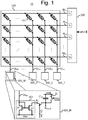
- Fig. 1 illustrates an example electronic device 10.
- the example electronic device 10 includes a memristor crossbar array 100, row driver circuitry 200, and a number of column output circuits 300 that each correspond to one of the column lines CL of the memristor crossbar array 100.
- the memristor crossbar array 100 may include N row lines RL (where N ⁇ 1), M column lines CL (where M ⁇ 1), and a number of memristors 101 that each are connected between one of the row lines RL and one of the column lines CL.
- each intersection of a row line RL with a column line CL may have a corresponding memristor 101.
- row line RL 1 corresponds to digital input value x 1
- row line RL 2 corresponds to digital input value x 2 , and so on.
- the memristor crossbar array 100 and column output circuits 300 may form a number of memristor-based analog MACs.
- each column line CL corresponds to an individual MAC.
- an individual MAC may comprise a column output circuit 300, the column line CL that is connected to the column output circuit 300, and the memristors 101 that are connected to the column line CL.
- An individual MAC may have N inputs, each corresponding to one of the row lines RL n ; specifically, an individual input of a given MAC may comprise the memristor 101 that is connected to the corresponding row line RL n .
- Each input of a given MAC may be assigned a weighting by setting the conductance G RL n of the corresponding memristor 101 to a value that corresponds to the desired weight.
- the row driver circuitry 200 serves as an input stage of the crossbar array 100, and may apply analog voltages to the row lines RL across a plurality of time periods based on the digital input vector X according to a distributed digital-to-analog conversion architecture. Specifically, in certain examples the row driver circuitry 200 may apply a plurality of analog voltages V 1 , V 2 , ...
- V P to a first node 220 during a plurality of time periods t 1 , t 2 , ..., t P , respectively, and, for each of the row lines RL, selectively connect the row line RL n to the first node 220 during one of the plurality of time periods t 1 , t 2 , ..., t P based on the corresponding digital input value x n of the digital input vector X .
- any row lines RL n whose digital input value x n is equal to "1" may be connected to the first node 220 during the first time period t 1
- any row lines RL n whose digital input value x n is equal to "2" may be connected to the first node 220 during the first time period t 2
- An example of the row driver circuitry 200 is described in greater detail below in relation to Fig. 2 .
- the column output circuits 300 may each include an integration capacitor C int , a switch S 1 that is controlled by an integration control signal Ctr_Int, and current mirroring circuitry 301 that is to, when the switch S 1 is closed, flow an integration current to or from an electrode of the integration capacitor C int whose magnitude mirrors a current flowing on the corresponding column line CL.
- the current mirroring circuitry 301 is to flow an integration current "to or from” an electrode of the integration capacitor C int (or the like)
- the integration capacitor C int may have a first electrode connected to the switch S 1 and a second electrode connected to a high voltage Vdd.
- An output node N out may be connected to the first electrode of the integration capacitor C int such that a voltage V C of the first electrode may be read out via output node N out , thereby enabling the voltage difference ⁇ V C stored in the integration capacitor to be ascertained.
- a reset switch S 2 may also be included between the high voltage Vdd and the first electrode, which may be controlled by a reset signal to reset the voltage difference ⁇ V C stored in the integration capacitor C int to zero.
- each of the column output circuits 300 may include similar features in similar configurations (except for being connected to different column lines CL), and therefore the example column output circuit 300_M that is illustrated in the expanded view may be representative of all of the column output circuits 300, and duplicative illustrations are omitted.
- the example current mirroring circuitry 301 includes a first transistor T 1 connected between the corresponding column line CL and a low voltage Vss (also referred to as a "first voltage") and a second transistor T 2 connected between the low voltage Vss and the switch S 1 , with the gate electrodes of the first and second transistors T 1 and T 2 being connected together and to the corresponding column line CL.
- the example current mirroring circuitry 301 illustrated in Fig. 1 will, when the switch S 1 is closed, flow charge away from the integration capacitor C int at a rate that is based on the current flowing on the corresponding column line CL.
- the electronic device 10 may be configured to process the digital input vector X during a processing period that comprises at least the time periods t 1 , t 2 , ..., t P .
- the row driver circuitry 200 may apply a voltage to the first node 220 during each of the time periods t 1 , t 2 , ..., t P .
- the integration control signal Crt_Int is to close the switch S 1 for a specified amount of time t int .
- Crt_Int may be pulsed high during each of the time periods t 1 , t 2 , ..., t P with a width of the pulse being t int , where t int is smaller than the duration of any of the time periods t 1 , t 2 , ..., t P .
- the timings at which Crt_Int is pulsed may be set such that transient effects resulting from the changing of voltages that are applied to the row lines RL may have subsided before Crt_Int is pulsed.
- the integration control signal Crt_Int may be pulsed a period of time ⁇ t after the start of each of the time periods t 1 , t 2 , ..., t P , where ⁇ t is set so as to avoid any transient effects.
- the integration control signal Crt_Int may be pulsed at timings that are ⁇ t ⁇ 1 ⁇ 2t A after the start of each of the time periods t 1 , t 2 , ..., t P .
- t int may be less than 1 ⁇ 2 ⁇ t A .
- a charge packet Q p is subtracted from (or, in some examples, added to) the first electrode of the capacitor C int , where the magnitude of Q p depends on the current I p that is flowing on the corresponding column CL during t p .
- the charge packet Q p is subtracted from or added to the first electrode depends on the configuration of the current mirroring circuitry 301.
- the example current mirroring circuitry 301 illustrated in Fig. 1 is to cause the charge packet Q p to be subtracted from the first electrode.
- the voltage difference ⁇ V C may be determined from the voltage V C output via the output node N out , and an output value y m for the corresponding column line CL may be generated based on ⁇ V C .
- the outputting of the voltage V C may include, for example, selectively connecting the node N out to a subsequent processing stage (e.g., via a switch (not illustrated)) and/or sampling the voltage V C of the node N out .
- the voltage V C of the output node N out may be output to an analog buffer or an ADC from which the output value y m may be generated.
- the voltage V C of the output node N out may be sampled and the output value y m may be generated based on the sampled voltage (V samp ).
- Fig. 3 illustrates an example in which the output values y 1 through y M are digital values
- Fig. 4 illustrates an example in which the output values y' 1 through y' M are analog values.
- the timings at which voltages are applied to row lines RL may vary according to the digital input vector X .
- the timings at which voltages are applied to row lines RL may vary according to the digital input vector X .
- the column output circuitry 300 may be able to generate the desired MAC result.
- the third row RL 3 will have the voltage V 2 applied thereto, since the digital input value x 3 for the row RL 3 is equal to "2".
- a charge packet Q 2 with magnitude t int V 2 G RL_3 will be subtracted from (or, in some examples, added to) the integration capacitor C int .
- no row lines RL will have the voltage V 3 applied thereto, since none of the digital input values x n are equal to "3".
- the charge on the electrode of the integration capacitor C int is unchanged.
- the second row RL 2 will have the voltage V 4 applied thereto, since the digital input value x 2 for the row RL 2 is equal to "4".
- a charge packet Q 4 with magnitude t int V 4 G RL_2 will be subtracted from (or, in some examples, added to) the integration capacitor C int . If there are any additional time periods after t 4 , then no voltages are applied to the row lines during those time periods, since none of the digital input values are greater than "4".
- the voltage difference ⁇ V C of the integration capacitor C int will be (t int /C int )(V 1 G RL_1 + V 4 G RL_2 + V 2 G RL_3 + V 1 G RL_4 ), which is the desired MAC result scaled by the constant (t int /C int ).
- the crossbar array 100 is illustrated as having four or more row lines RL and four or more column lines CL, but this is merely one example used for convenience of description and any numbers of row lines RL and column lines CL greater than or equal to one may be included.
- additional row lines may be provided in the crossbar array 100 that do not correspond to a digital input value x n of the digital input vector X .
- an offset line may be included that may be used for providing adjustable offsets for each MAC, but which does not have a corresponding digital input value x n .
- any references to "row lines” mean those row lines that correspond to a digital input value x n of the digital input vector X and not any other row lines that might be included in the crossbar array 100, unless specifically indicated otherwise.
- a phrase such as "each of the row lines” should be understood to refer to each row line that corresponds to a digital input value x n of the digital input vector X and not to other possible row lines (such as an offset line), unless specifically indicated otherwise.
- Fig. 1 the voltages Vss and Vdd are illustrated, where Vdd > Vss. It should be understood that, in certain examples, the voltages Vss and Vdd could be reversed, such that Vdd is applied wherever Vss is illustrated as being applied and vice-versa. Such a reversal may also entail changing the polarities of various signals, changing directions in which various currents flow, changing the polarities of various transistors, and the like.
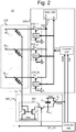
- Fig. 2 illustrates portions of an example electronic device 10 in greater detail.
- Fig. 2 illustrates an example of the row driver circuitry 200, as well as a controller 400.
- Various elements of Fig. 2 correspond to elements of Fig. 1 that were already described above, and the same reference numbers are used in both Figures for such corresponding elements. Duplicative description of such corresponding features is omitted.
- the example row driver circuitry 200 includes a switching circuit 210 for each of the row lines RL, the first node 220, a digital-to-analog converter ("DAC") 230, and a counter 240.
- DAC digital-to-analog converter
- each of the switching circuits 210 may include a switch connected between the row line RL and the node 220 and a comparison circuit 211 that is to close the switch at the appropriate timing.
- the comparison circuit 211 may store the digital input value of the corresponding row line RL and may compare the stored digital value to the digital value COUNT output by the counter 240, and may close the switch when the stored digital value matches COUNT.
- the comparison circuit 211 may include a register to store the digital input value and a comparator to compare the stored value with COUNT, an output of the comparator controlling the switch.
- the DAC 230 may be to apply the voltages V 1 to V P to the node 220 during the time periods t 1 to t P , respectively.
- the DAC 230 may generate an analog voltage signal V ramp based on a digital value COUNT whose value may change at the start of each time period t 1 to t P according to the clock signal Clk.
- the signal V ramp may step through the voltages V 1 to V P during the time periods t 1 to t P , where V 1 is an analog voltage corresponding to the value of COUNT during t 1 , V 2 is an analog voltage corresponding to the value of COUNT during t 2 , and so on.
- the counter 240 may output a digital signal COUNT, whose value may change at the start of each of the time periods t 1 - t P according to the clock Clk.
- the counter 240 may be configured to increment a value of COUNT each time period, in which case the signal V ramp may take the form of a ramp signal whose magnitude increases during each time period.
- the controller 400 may include circuitry to generate the clock signal Clk, the reset signal, and the integration control signal Crt_Int.
- the clock signal Clk may be any clock signal.
- the controller 400 may assert the reset signal after the P th time period t P to reset the counter 240 and the integration capacitor C int of each of the column output circuits 300.
- the controller 400 may release the reset signal when a new processing period is begun for a new digital input value X .
- the integration control signal Crt_Int may be generated based on the clock signal Clk. For example, as illustrated in Fig.
- a second clock signal Clk 2 with a same period as the clock signal Clk may be generated, a third signal Clk 3 may be generated from the second signal Clk 2 by shifting a phase of the second signal Clk 2 by an amount ⁇ , and then the integration control signal Crt_Int may be generated from the third signal Clk 3 by truncating each active pulse of the third signal Clk 3 such that the period of the active pulses remains the same but their pulse width is made equal to t int .
- the active pulses of the third signal Clk 3 may correspond to whichever logical value causes the switches S 1 to be closed.
- the electronic device 10 may include an artificial neural network ("ANN").
- ANN artificial neural network
- the crossbar array 100, the row driver circuitry 200, and the column output circuits 300 may correspond to a first layer of the ANN.
- each MAC of the crossbar array 100 may correspond to an induvial neuron.
- each column may correspond to an individual neuron, and the neuron may include each of the memristors 101 in the corresponding column together with the column output circuit 300 of the corresponding column.
- each column of the crossbar array 100 corresponds to exactly one neuron (e.g., there is a one-to-one correspondence between columns and neurons), while in other examples (e.g., see Fig.
- more than one column may correspond to multiple neurons (e.g., there is a many-to-one correspondence between columns and neurons).
- Figs. 3 and 4 illustrate examples in which the electronic device 10 includes multiple layers of an ANN.
- Fig. 3 illustrates an example in which the electronic device 10 includes an ANN and in which the output values y 1 - y M of the first layer are digital output values.
- Various elements of Fig. 3 correspond to elements of Fig. 1 that were already described above, and the same reference numbers are used in both Figures for such corresponding elements. Duplicative description of such corresponding features is omitted. Details of the column output circuit 300_M and the output circuit 500 are illustrated in an expanded view indicated by dashed lines.
- a first layer of the ANN is formed by the crossbar array 100, the row driver circuitry 200, and the column output circuits 300.
- the example electronic device 10 also includes an output circuit 500 that generates the digital output values y 1 - y M (collectively the digital output vector Y ) based on the voltage differences ⁇ V C of the column output circuits 300_1 to 300_M, respectively, and feeds the digital output values y 1 - y M to an input stage 2000 of a second layer 1000 of the ANN.
- the output node N out of each of the column output circuits 300 may be connected to the output circuit 500, such that the respective voltages V C of the column output circuits 300 may be output to the output circuit 500.
- the output circuit 500 may include an analog-to-digital converter ("ADC") 502 that is to generate a digital output value y m that corresponds to the voltage difference ⁇ V C of the m th column output circuit 300 based on the voltage V C that is output via the output node N out_m (or based on another analog voltage that itself is based on V C , such as a sampled voltage V samp ) with the voltage Vdd serving as a reference voltage.
- ADC analog-to-digital converter
- a separate ADC 502 may be provided for each of the column output circuits 300.
- the multiple column output circuits 300 may share the same ADC 502.
- the output circuit 500 is illustrated as also including sample-and-hold circuits ("S/H") 501 that are to sample the voltage V C and provide a sampled voltage V samp to the ADC 502.
- S/H sample-and-hold circuits
- a separate S/H 501 may be provided for each column output circuit 300.
- the S/H 501 circuits may be omitted and the voltages V C may be fed directly to the ADC 502.
- the second layer 1000 of the ANN and its associated input stage 2000 may be configured to receive digital input vectors and output digital output vectors, similar to the first layer of the example device 10 in Fig. 3 .
- the second layer 1000 of the ANN and its associated input stage 2000 may have a similar configuration as that of the first layer.
- the second layer 1000 may include a crossbar array that is similar to the crossbar array 100 and column output circuits that are similar to the column output circuits 300, and the input stage 2000 may be similar to the row driver circuitry 200.
- additional layers of the ANN may be included (not illustrated), which may also be configured in a similar manner as the first layer. Such an approach may be beneficial in the sense that a uniform architecture is used for each layer.
- Fig. 4 illustrates an example in which the electronic device 10 includes an ANN and in which the output values y 1 - y M of the first layer are analog output values.
- Various elements of Fig. 4 correspond to elements of Fig. 1 that were already described above, and the same reference numbers are used in both Figures for such corresponding elements. Duplicative description of such corresponding features is omitted. Details of the column output circuit 300_M and the output circuit 600 are illustrated in an expanded view indicated by dashed lines.
- an apostrophe may be appended to the reference signs of the analog output values y 1 - y M and the output vector Y when referring specifically to the analog versions thereof to distinguish them from the digital versions thereof.
- a first layer of the ANN is formed by the crossbar array 100, the row driver circuitry 200, and the column output circuits 300.
- the example electronic device 10 also includes an output circuit 600 that generates the analog output values y' 1 - y' M (collectively the analog output vector Y') based on the voltage differences ⁇ V C of the column output circuits 300_1 to 300_M, respectively, and feeds the analog output values y' 1 - y' M to an input stage 2001 of a second layer 1001 of the ANN.
- the output node N out of each of the column output circuits 300 may be connected to the output circuit 600, such that the respective voltages V C of the column output circuits 300 may be output to the output circuit 600.
- the output circuit 600 may include a buffer 602 for each column output circuit 300 that generates the corresponding analog output value y' m based on the voltage difference ⁇ V C of the column output circuit 300 (or based on another analog voltage that itself is based on ⁇ V C ).
- the buffer 602 may include a differential amplifier that amplifies a difference between the voltage V C (or a corresponding voltage) and the high voltage Vdd to a level that is suitable for transfer to the second layer via an analog signal bus.
- the buffer 602 may include circuitry for converting the voltage difference ⁇ V C to a current for transfer to the second layer via a current-based analog signal bus.
- the output circuit 500 is illustrated as also including sample-and-hold circuits ("S/H") 601 that sample the voltage V C and provide a sampled voltage V samp to the corresponding buffer 602.
- S/H sample-and-hold circuits
- a separate S/H 601 may be provided for each column output circuit 300.
- the S/H 601 circuits may be omitted and the voltages V C may be fed directly to the buffer 602.
- the second layer 1001 of the ANN and its associated input stage 2001 may be configured to receive an analog input vector and generate an analog output vector.
- the second layer 1001 of the ANN and its associated input stage 2001 may have a different configuration from that of the first layer.
- the second layer 1001 may include a crossbar array that is similar to the crossbar array 100, but column output circuits thereof may be different from the column output circuits 300 and the input stage 2001 may be different from the row driver circuitry 200.
- the input stage 2001 may be configured to apply the analog output values y 1 - y P directly to row lines of the second layer 1001 simultaneously, and the column output circuits of the second layer 1001 may be configured to sense an aggregate current flowing on each column line as a result of the applied voltages.
- additional layers of the ANN may be included (not illustrated), which may also be configured in a similar manner as the second layer 1001. Such an approach may be beneficial in that analog-to-digital conversion circuitry may be omitted from each layer, which may reduce cost and save chip space.
- weights may be independently set for each input (i.e., for each row line RL) of each of the individual MACs by setting the conductances of the corresponding memristors 101.
- the weights for the inputs of a given MAC may all be positive or they may all be negative, but positive weights and negative weights cannot be set for different inputs of the same individual MAC.
- Fig. 5 illustrates another example of the electronic device 10 in which both positive and negative weights may be assigned to the inputs of the same individual MAC.
- Fig. 5 illustrates an example device 10 that includes a crossbar array 110, row driver circuitry 200, and column output circuits 310.
- Various elements of Fig. 5 correspond to elements of Fig. 1 that were already described above, and the same references numbers are used in both Figures for such corresponding elements. Duplicative description of such corresponding features is omitted.
- the crossbar array 110 of Fig. 5 is similar to the crossbar array 100 described above, with the exception that the column lines CL of the crossbar array 110 include positive-weight column lines CL+ and negative-weight column lines CL-.
- the positive-weight column lines CL+ and the negative-weight column lines CL- are arranged in pairs, such that for each positive-weight column line CL+ there is a corresponding negative-weight column line CL-.
- a memristor 101 that is connected to one of the positive-weight column lines CL+ may occasionally be referred to as a positive memristor 101, while a memristor 101 that is connected to one of the negative-weight column lines CL- may occasionally be referred to as a negative memristor 101.
- the positive memristors 101 may be used to assign positive weights while the negative memristors 101 may be used to assign negative weights, as described in greater detail below.
- Each of the column output circuits 310 corresponds to a pair of column lines comprising one of the positive-weight column lines CL+ and its corresponding negative-weight column line CL-.
- an individual MAC may comprise a column output circuit 310, the positive-weight column line CL+ and its corresponding negative-weight column line CL- that are connected to the column output circuit 310, and the memristors 101 that are connected to the pair of column lines CL+/CL-.
- An individual MAC may have N inputs, each corresponding to one of the row lines RL n .
- an individual input of a given MAC may comprise the positive memristor 101 and the negative memristor 101 that are connected to the corresponding row line RL n .
- the column output circuits 310 of Fig. 5 are similar to the column output circuits 300 described above, with the exception that second mirroring circuitry 302 is provided in addition to the first mirroring circuitry 301, and the integration capacitor C int is connected to an intermediate voltage Vdd/2 rather than to the high voltage Vdd.
- the first mirroring circuitry 301 may be connected to the corresponding positive-weight column line CL+, while the second mirroring circuitry 302 may be connected to the corresponding negative-weight column line CL-.
- the second current mirroring circuitry 302 may be selectively connected to the integration capacitor C int via a corresponding switch S 3 that is controlled by the integration control signal Ctr_Int.
- the switch S 3 that selectively connects the second current mirroring circuitry 302 to the integration capacitor C int may be the same device as the switch S 1 that connects the first current mirroring circuitry 301 to the integration capacitor C int .
- the switch S 3 that selectively connects the second current mirroring circuitry 302 to the integration capacitor C int may be a separate device from the switch S 1 , as illustrated in Fig. 5 .
- the switch S 3 may be referred to as if it were separate from the switch S 1 for convenience, but it should be understood that the descriptions below may also apply to examples in which the switch S 3 and the switch S 1 are formed by the same device.
- the first current mirroring circuitry 301 may be used to, when the switch S 1 is closed, flow a first integration current to or from an electrode of the integration capacitor C int whose magnitude mirrors a current flowing on the corresponding positive-weight column line CL+.
- the second current mirroring circuitry 302 may be used to, when the switch S 3 is closed, flow a second integration current from or to the electrode of the integration capacitor C int whose magnitude mirrors a current flowing on the corresponding negative-weight column line CL-.
- the first and second current mirroring circuitry 301/302 are such that the first integration current and the second integration current flow in opposite directions relative to the electrode of the integration capacitor C int .
- the switch S 1 and the switch S 3 are controlled by the integration control signal Ctr_Int.
- the example first current mirroring circuitry 301 shown in Fig. 5 is used to flow current away from the first electrode of the integration capacitor C int
- the example second current mirroring circuitry 302 shown in Fig. 5 is used to flow current to the first electrode.
- the example second current mirroring circuitry 302 includes a third transistor T 3 connected between the corresponding negative-weight column line CL- and the low voltage Vss and a fourth transistor T 4 connected between the low voltage Vss and a fifth transistor T 5 , with the gate electrodes of the third and fourth transistors T 3 and T 4 being connected together and to the corresponding column line CL-.
- the example second current mirroring circuitry 302 also includes a fifth transistor T 5 connected between the fourth transistor T 4 and the high voltage Vdd, and a sixth transistor T 6 connected between the high voltage Vdd and the switch S 3 , with the gate electrodes of the fifth and six transistors T 5 and T 6 being connected together and to the fourth transistor T 4 .
- the fifth and six transistors T 5 and T 5 may be p-channeled transistors, while the first through fourth transistors T 1 - T 4 may be n-channeled transistors.
- Fig. 5 will, when the switch S 3 is closed, flow charge to the integration capacitor C int at a rate that is based on the current flowing on the corresponding negative-weight column line CL-.
- this is merely one example of the second current mirroring circuitry 302, and that any type of current mirror could be used as long as it is configured to, when the switch S 3 is closed, flow a second integration current to or from an electrode of the integration capacitor C int (in an opposite direction of the first integration current) whose magnitude mirrors a current flowing on the corresponding negative-weight column line CL-.
- charge packets are added to or subtracted from the first electrode of the capacitor C int , where the net amount of charge that is added/subtracted during t p (hereinafter Q' p ) depends on the current I p + that is flowing on the corresponding positive-weight column CL+ during t p and on the current I p - that is flowing on the corresponding negative-weight column CL- during t p .
- ⁇ p Q' p a net amount of charge equal to ⁇ p Q' p has been subtracted from the first electrode across all the time periods t 1 - t P
- a negative value of ⁇ p Q' p implies that a net amount of charge equal to ⁇ p Q' p has been added to the first electrode across all the time periods t 1 - t P .
- an n th input of a given MAC may be assigned a positive weighting by setting the conductance G RL n + of the positive memristor 101 of the n th row line RL n to a value that corresponds to the desired weight and setting the conductance G RL n ⁇ of the negative memristor 101 that is connected to the n th row line RL n to zero (or to a very low value).
- an n th input of a given MAC may be assigned a negative weighting by setting the conductance of the negative memristor 101 of the n th row line RL n to a value that corresponds to the desired weight and setting the conductance of the positive memristor 101 that is connected to the n th row line RL n to zero (or to a very low value).
- each input of a given MAC may have its associated positive and negative memristors 101 set independently from the memristors 101 of the other inputs of the same MAC, and therefore in such examples it is possible for one input of a MAC to be assigned a positive weight while another input of the same MAC is assigned a negative weight.
- the example electronic device 10 illustrated in Fig. 5 may include an artificial neural network ("ANN").
- the crossbar array 110, the row driver circuitry 200, and the column output circuits 310 may correspond to a first layer of the ANN.
- each MAC of the crossbar array 110 may correspond to an induvial neuron.
- each pair of column lines CL+ and CL- may correspond to an individual neuron, and the neuron may include each of the memristors 101 in the corresponding columns together with the column output circuit 310 of the corresponding columns.
- There may be additional layers of the ANN subsequent to the first layer, in which case the output Y (y 1 , y 2 , ..., y M ) of the first layer may be fed to the second layer as an input thereof.
- the example electronic device 10 illustrated in Fig. 5 may include the output circuitry 500, as well as the second layer 1000 and its associated input stage 2000 as described above and illustrated in Fig. 3 .
- the output circuitry 500, second layer 1000, and input stage 2000 may be configured in the same manner described above in relation to Fig. 3 , and therefore duplicative description of these features is omitted.
- the example electronic device 10 illustrated in Fig. 5 may include the output circuitry 600, as well as the second layer 1001 and its associated input stage 2001 as described above and illustrated in Fig. 4 .
- the output circuitry 600, second layer 1001, and input stage 2001 may be configured in the same manner described above in relation to Fig. 4 , and therefore duplicative description of these features is omitted.
- Fig. 6 illustrates an example method of operating an electronic device.
- the method may be for operating an artificial neural network that has a first layer comprising a crossbar array (such as the crossbar array 100 or 110) with row lines, column lines, and memristors that each are connected between one of the row lines and one of the column lines.
- the example method may be performed, for example, via one or more controllers of the electronic devices, such as, for example, the controller 400.
- the example method includes applying a plurality of analog voltages to a first node during a plurality of time periods, respectively (see block 6001).
- voltages V 1 - V P may be applied to the first node during time period t 1 - t P , respectively, where P ⁇ 2.
- the example method may also include, for each of the row lines, selectively connecting the row line to the first node during one of the plurality of time periods based on a digital input vector (see block 6002).
- the row line RL n may be selectively connected to the first node at one of the time periods t 1 -t P based on digital input x n that corresponds to the row line RL n .
- Connecting a given row line RL n to the first node in accordance with block 6002 may result in the voltage V p being applied to the given row line RL n , since V p is applied to the first node during t p in accordance with block 6001.
- the example method may also include, for each of the column lines, closing at least one switch corresponding to the column line for a specified amount of time (t int ) during each of the plurality of time periods, and, while the at least one switch is closed, causing an integration current to flow to or from an integration capacitor corresponding to the column line whose magnitude mirrors a current flowing on the column line (see block 6003).
- the at least one switch of each of the column lines may be controlled in the manner described above by applying an integration control signal (such as Ctr_Int) to the switches.
- the integration control signal may be pulsed to an active level during each of the time period t 1 - t P with a pulse width equal to the specified amount of time (tint).
- the causing of the integration current to flow to or from the integration capacitor when the at least one switch is closed may be achieved via a current mirroring circuit (such as the current mirroring circuit 301) that is connected between the column line and the switch.
- causing the integration current to flow to or from the integration capacitor when the at least one switch is closed may include applying a first voltage (e.g., Vss) to the current mirroring circuit at least while the switch is closed.
- the example method may also include generating an output vector for the first layer based on the respective voltages that are stored in the integration capacitors of the column lines after an end of the plurality of time periods (see block 6004).
- the crossbar array may further include second column lines that each correspond to one of the column lines and second memristors that each are connected between one of the row lines and one of the second column lines (such as in the crossbar array 310).
- the method may further include at block 6003 for each of the column lines: while the at least one switch of the column line is closed, causing a second integration current to flow to or from the integration capacitor of the column line whose magnitude mirrors a current flowing on the one of the second column lines that corresponds to the column line, where the first integration current and the second integration current flow in opposite directions relative to the integration capacitor of the column line.
- each neuron of the first layer is associated with one of the column lines and a corresponding one of the second column lines.
- the example method may further comprise: setting a positive weight for a first given input of a given neuron by adjusting a resistance of one of the memristors that is connected to the associated column line, and setting a negative weight for a second given input of the given neuron by adjusting a resistance of one of the memristors that is connected to the associated second column line.
- the output vector for the first layer is a digital output vector.
- generating the output vector for the first layer at block 6004 may include feeding signals based on the respective voltages stored in the integration capacitors of the column lines after the end of the plurality of time periods to at least one analog-to-digital converter.
- the signals fed to the at least one analog-to-digital converter may be voltages sampled from the voltages stored in the integration capacitors by sample-and-hold circuits.
- the output vector for the first layer is an analog output vector.
- generating the output vector for the first layer at block 6004 may include feeding signals based on the respective voltages stored in the integration capacitors of the column lines after the end of the plurality of time periods to analog buffer circuitry.
- the signals fed to the analog buffer circuitry may be voltages sampled from the voltages stored in the integration capacitors by sample-and-hold circuits.
- the term “memristor” may be used in certain contexts in a broad sense and may be used in certain contexts in a narrow sense.
- “memristor” may refer specifically to circuit elements that exhibit a non-linear relationship between electric charge and magnetic flux (or exhibit a relationship between the time integral of current and the time integral of voltage).
- “memristor” refers broadly to any non-volatile memory element that is based on changing resistance states and is read by its resistance.
- memristor is always used in the broad sense, unless specifically indicated otherwise; specifically, as used herein, “memristor” refers broadly to any non-volatile memory element that is based on changing resistance states and is read by its resistance.
- the memristors 101 may be formed by, for example, a memristor in the narrow sense of the term, a memory element that changes the resistance across a dielectric solid-state material, a phase-change memory element (sometimes referred to as PCM or PCRAM), a conductive-bridging memory element (sometimes referred to as CBRAM or a programmable metallization cell), a magnetoresistive memory element (sometimes referred to as MRAM), or the like.
- PCM phase-change memory element
- CBRAM conductive-bridging memory element
- MRAM magnetoresistive memory element
- resistive elements that are not memristors may be used in place of the memristors 101 to connect the column lines and row lines in the crossbar array 100.
- Such resistive elements may be, for example, variable resistance resistors or fixed resistance resistors.
- a variable resistance resistor include a transistor operating in liner (ohmic) mode (in which case the channel resistance thereof may be varied by varying a voltage applied to the gate of the transistor), a circuit element that changes its resistance by changing a current path through the circuit element (for example, multiple resistors with different resistances and a switch that selects which of the resistors the current path flows through), and the like.
- Examples of fixed resistance resistors include poly resistors, laser-trimmed thin films, and the like.
- the other components of the example device 10 may be in the same configurations as those described above; in some such examples, additional components specific to the resistive elements may also be added as needed (e.g., gate lines for transistors, control lines for switches, etc.).
- the weights that are assigned to inputs of the MACs may be dynamically adjusted by changing the conductances of the memristors 101 or variable resistance resistors.
- the weights that are assigned to the inputs of the MACs may be set (e.g., during manufacture) and may thereafter remain fixed.
- an electronic device comprises:
- an output signal thereof is based on a voltage difference stored in the integration capacitor after an end of the plurality of time periods.
- analog-to-digital conversion circuitry to generate a digital output value for each of the column output circuits based on respective voltage differences stored in the integration capacitors of the column output circuits after an end of the plurality of time periods.
- analog buffer circuitry to output an analog output value for each of the column output circuits based on respective voltage differences stored in the integration capacitors of the column output circuits after an end of the plurality of time periods.
- the crossbar array, the row driver circuitry, and the column output circuits form a first layer of an artificial neural network, with each neuron of the first layer being associated with one of the first column lines and its corresponding second column line, the electronic device sets a positive weight for a first given input of a given neuron by adjusting a resistance conductance of one of the memristors that is connected to the associated first column line, and the electronic device sets a negative weight for a second given input of the given neuron by adjusting a conductance of one of the memristors that is connected to the associated second column line.
- A, B, and/or C may include any one of: ⁇ A ⁇ , ⁇ B ⁇ , ⁇ C ⁇ , ⁇ A, B ⁇ , ⁇ A, C ⁇ , ⁇ C, B ⁇ , and ⁇ A, C, B ⁇ .
Landscapes
- Engineering & Computer Science (AREA)
- Physics & Mathematics (AREA)
- Theoretical Computer Science (AREA)
- General Physics & Mathematics (AREA)
- Software Systems (AREA)
- Computing Systems (AREA)
- General Engineering & Computer Science (AREA)
- Biomedical Technology (AREA)
- Health & Medical Sciences (AREA)
- Life Sciences & Earth Sciences (AREA)
- Mathematical Physics (AREA)
- Biophysics (AREA)
- Pure & Applied Mathematics (AREA)
- Mathematical Optimization (AREA)
- Computational Mathematics (AREA)
- Mathematical Analysis (AREA)
- Data Mining & Analysis (AREA)
- Evolutionary Computation (AREA)
- General Health & Medical Sciences (AREA)
- Molecular Biology (AREA)
- Artificial Intelligence (AREA)
- Computational Linguistics (AREA)
- Neurology (AREA)
- Power Engineering (AREA)
- Computer Hardware Design (AREA)
- Fuzzy Systems (AREA)
- Algebra (AREA)
- Automation & Control Theory (AREA)
- Analogue/Digital Conversion (AREA)
- Electronic Switches (AREA)
Description
- A multiplier-accumulator (MAC) is a device that performs a multiply-accumulate operation. For example, the multiply-accumulate operation may include multiplying various values and adding the products together.
- An artificial neuron may include circuitry that receives one or more input signals and performs operations on the inputs to generate an output signal. The input signals and output signals may be, for example voltages, currents, digital values, etc. In certain examples, the operations performed by an artificial neuron on the inputs may include multiply-accumulate operations, in which case the artificial neuron may include a MAC. In such examples, the input signals of the neuron may be fed to the MAC for multiplication with other values (e.g., weightings that are set for each input) and the output signal of the neuron may be based on the output signal of the MAC. Artificial neural networks are collections of artificial neurons in which the output signals of some neurons are used as the input signals of other neurons.
-
-
Fig. 1 is a circuit diagram illustrating an example electronic device that includes memristor-based analog MACs. -
Fig. 2 is a circuit diagram illustrating example row driver circuitry. -
Fig. 3 is block diagram illustrating an example electronic device that includes multiple neural network layers and output circuitry for generating a digital output vector. -
Fig. 4 is block diagram illustrating an example electronic device that includes multiple neural network layers and output circuitry for generating an analog output vector. -
Fig. 5 is a circuit diagram illustrating an example electronic device that includes memristor-based analog MACs that each has a positive-weight column and a negative-weight column. -
Fig. 6 is a process flow diagram illustrating an example method of operating an electronic device that includes memristor-based analog MACs. -
Fig. 7 is a signal timing diagram illustrating a clock signal, an integration control signal, and various intermediate clock signals that may be used to generate the integration control signal from the clock signal. - An example electronic device may include a number of memristor-based analog MACs. A memristor-based analog MAC is a MAC that performs the multiply-accumulate operation in the analog domain, using one or more memristors to perform a multiply portion of the multiply-accumulate operation. For example, voltages may be applied across the memristors and the resulting currents flowing through the memristors may be summed. The conversion of voltage to current represents the multiply portion of the multiply-accumulate operation in the analog domain, since the current flowing through each memristor equals the conductance of the memristor multiplied by the voltage applied across the memristor. Thus, the desired multiplications may be made in the analog domain by appropriately setting the conductances of the memristors and the voltages applied thereto.
- Certain example electronic devices described herein may include multiple such memristor-based analog MACs. For example, the example electronic devices may include a memristor crossbar array, which may include column lines, row lines, and memristors arranged in an array with each of the memristors connected between one of the column lines and one of the row lines. A column output circuit may be included for each column line, with each column of memristors and its corresponding column output circuit forming a MAC. In such examples, voltages may be applied to the rows of the crossbar array based on an input vector, and an output vector may be determined based on the currents flowing through the memristors as a result of the applied voltages. An input stage may be used to generate the appropriate voltages for each row based on the input vector. For example, the crossbar array may form one layer of neurons in an artificial neural network ("ANN"), with each of the MACs forming an artificial neuron and weights for the neurons being set by adjusting the conductances of the corresponding memristors.
- In certain examples, an input stage of the crossbar array may apply analog voltages to the row lines based on a digital input vector-specifically, the digital input vector may include a digital value for each row line, and the analog voltages that are applied to the row lines may be based on the respective digital values of the row lines. In certain examples, the input stage may employ a distributed digital-to-analog conversion architecture in which a single voltage source is used to generate the voltages for all of the row lines across a number of time periods. In particular, in such a distributed digital-to-analog conversion architecture, a voltage source (such as the digital-to-
analog converter 230 inFig. 2 ) may generate a signal that steps through a series of voltages V1, V2, ... VP in time periods t1, t2, ..., tP, respectively, and switching units (such as the switching units 210) may be provided for each row to connect that row to the voltage signal when the signal is at the appropriate voltage for that row according to the input digital value for that row. For example, each row (if any) with a digital input value of "1" may be connected to the voltage source during time period t1 (and thus the voltage V1 would be applied to those rows), each row (if any) with a digital input value of "2" may be connected to the voltage source during time period t2 (and thus the voltage V2 would be applied to those rows), and so on. In this manner, each row may have the appropriate analog voltage applied thereto based on the row's input digital value without having to include a digital-to-analog converter for each row line. - The column output circuitry for each column line may be configured to generate an output signal that corresponds to a sum of the currents that flow on the corresponding column line. However, when a distributed digital-to-analog conversion architecture is used, the voltages are not necessarily applied to the row lines simultaneously, and therefore the currents may flow through the various memristors at different timings. Thus, in order to obtain the output signal that corresponds to a sum of the currents flowing on the corresponding column line, in certain examples each column output circuit may include an integration capacitor, a switch that is controlled by an integration control signal, and current mirroring circuitry that is to, when the switch is closed, flow an integration current to or from an electrode of the integration capacitor whose magnitude mirrors a current flowing on the corresponding column line, and the integration control signal may close the switch for a specified amount of time during each of the plurality of time periods. As a result, by the end of the Pth time period tP, for each column output circuit a voltage difference stored in the integration capacitor will be proportional to the sum of all the currents that flowed on the column line from time periods t1 to tP, which is the desired MAC result scaled by a constant. Specifically, the voltage difference stored in the integration capacitor will be

- By using the example column output circuits described above, certain examples are able to avoid having to provide sample-and-hold circuits for each row line. Specifically, one alternative approach to generating an output signal that corresponds to a sum of the currents that flow on the corresponding column line would be to cause all of the currents to flow at the same time and then sense the resulting aggregate current. However, when a distributed digital-to-analog conversion architecture is used, in order to ensure that all of the currents flow on the corresponding column line at the same time, some mechanism for holding the disparate voltages that are generated for the row lines across the time periods t1 to tP (such as a sample-and-hold circuit for each row line) may be needed so that the respective voltages may be applied to the row lines simultaneously. Such sample-and-hold circuits may take up chip space and increase a cost of the device, and therefore examples described herein that are able to omit such per-row sample-and-hold circuits as a result of using the example column output circuits described above may have reduced costs and improved chip space usage.
-
Fig. 1 illustrates an exampleelectronic device 10. The exampleelectronic device 10 includes amemristor crossbar array 100,row driver circuitry 200, and a number ofcolumn output circuits 300 that each correspond to one of the column lines CL of thememristor crossbar array 100. - The
memristor crossbar array 100 may include N row lines RL (where N ≥ 1), M column lines CL (where M ≥ 1), and a number ofmemristors 101 that each are connected between one of the row lines RL and one of the column lines CL. In certain examples, each intersection of a row line RL with a column line CL may have acorresponding memristor 101. Each of the row lines RLn may correspond to a digital input value xn of a digital input vectorX = (x1, x2, ..., XN). Specifically, row line RL1 corresponds to digital input value x1, row line RL2 corresponds to digital input value x2, and so on. - The
memristor crossbar array 100 andcolumn output circuits 300 may form a number of memristor-based analog MACs. For example, inFig. 1 each column line CL corresponds to an individual MAC. Specifically, an individual MAC may comprise acolumn output circuit 300, the column line CL that is connected to thecolumn output circuit 300, and thememristors 101 that are connected to the column line CL. An individual MAC may have N inputs, each corresponding to one of the row lines RLn; specifically, an individual input of a given MAC may comprise thememristor 101 that is connected to the corresponding row line RLn. Each input of a given MAC may be assigned a weighting by setting the conductance GRLn of thecorresponding memristor 101 to a value that corresponds to the desired weight. Although there may be many MACs included in theexample device 10, portions of the description below may focus on a single MAC for ease of description, especially when describing features that are common to each of the MACs. - The
row driver circuitry 200 serves as an input stage of thecrossbar array 100, and may apply analog voltages to the row lines RL across a plurality of time periods based on the digital input vectorX according to a distributed digital-to-analog conversion architecture. Specifically, in certain examples therow driver circuitry 200 may apply a plurality of analog voltages V1, V2, ... VP to afirst node 220 during a plurality of time periods t1, t2, ..., tP, respectively, and, for each of the row lines RL, selectively connect the row line RLn to thefirst node 220 during one of the plurality of time periods t1, t2, ..., tP based on the corresponding digital input value xn of the digital input vectorX . For example, any row lines RLn whose digital input value xn is equal to "1" may be connected to thefirst node 220 during the first time period t1, any row lines RLn whose digital input value xn is equal to "2" may be connected to thefirst node 220 during the first time period t2, and so on. An example of therow driver circuitry 200 is described in greater detail below in relation toFig. 2 . - The
column output circuits 300 may each include an integration capacitor Cint, a switch S1 that is controlled by an integration control signal Ctr_Int, andcurrent mirroring circuitry 301 that is to, when the switch S1 is closed, flow an integration current to or from an electrode of the integration capacitor Cint whose magnitude mirrors a current flowing on the corresponding column line CL. When it is said that thecurrent mirroring circuitry 301 is to flow an integration current "to or from" an electrode of the integration capacitor Cint (or the like), this should be understood to mean that one possible configuration of thecurrent mirroring circuitry 301 is to flow current to the integration capacitor Cint while another possible configuration of thecurrent mirroring circuitry 301 is to flow current away from the integration capacitor Cint. The integration capacitor Cint may have a first electrode connected to the switch S1 and a second electrode connected to a high voltage Vdd. An output node Nout may be connected to the first electrode of the integration capacitor Cint such that a voltage VC of the first electrode may be read out via output node Nout, thereby enabling the voltage difference ΔVC stored in the integration capacitor to be ascertained. In certain examples, a reset switch S2 may also be included between the high voltage Vdd and the first electrode, which may be controlled by a reset signal to reset the voltage difference ΔVC stored in the integration capacitor Cint to zero. - Details of one of the column output circuits 300 (namely, the column output circuit 300_M) are illustrated in
Fig. 1 in an expanded view indicated by dashed lines. In certain examples, each of thecolumn output circuits 300 may include similar features in similar configurations (except for being connected to different column lines CL), and therefore the example column output circuit 300_M that is illustrated in the expanded view may be representative of all of thecolumn output circuits 300, and duplicative illustrations are omitted. - One possible example of the
current mirroring circuitry 301 is illustrated inFig. 1 . The examplecurrent mirroring circuitry 301 includes a first transistor T1 connected between the corresponding column line CL and a low voltage Vss (also referred to as a "first voltage") and a second transistor T2 connected between the low voltage Vss and the switch S1, with the gate electrodes of the first and second transistors T1 and T2 being connected together and to the corresponding column line CL. The examplecurrent mirroring circuitry 301 illustrated inFig. 1 will, when the switch S1 is closed, flow charge away from the integration capacitor Cint at a rate that is based on the current flowing on the corresponding column line CL. It should be understood that this is merely one example of thecurrent mirroring circuitry 301, and that any type of current mirror could be used as long as is configured to, when the switch S1 is closed, flow an integration current to or from an electrode of the integration capacitor Cint whose magnitude mirrors a current flowing on the corresponding column line CL. - The
electronic device 10 may be configured to process the digital input vectorX during a processing period that comprises at least the time periods t1, t2, ..., tP. As noted above, therow driver circuitry 200 may apply a voltage to thefirst node 220 during each of the time periods t1, t2, ..., tP. In addition, during each of the time periods t1, t2, ..., tP, the integration control signal Crt_Int is to close the switch S1 for a specified amount of time tint. For example, if the switch S1 is configured to be closed when Crt_Int is at a high logical value, then Crt_Int may be pulsed high during each of the time periods t1, t2, ..., tP with a width of the pulse being tint, where tint is smaller than the duration of any of the time periods t1, t2, ..., tP. The timings at which Crt_Int is pulsed may be set such that transient effects resulting from the changing of voltages that are applied to the row lines RL may have subsided before Crt_Int is pulsed. For example, since the voltages applied to the row lines RL change at the start of each time of the time periods t1, t2, ..., tP, the integration control signal Crt_Int may be pulsed a period of time Δt after the start of each of the time periods t1, t2, ..., tP, where Δt is set so as to avoid any transient effects. For example, if tA is the duration of each of the time periods t1, t2, ..., tP, then the integration control signal Crt_Int may be pulsed at timings that are Δt ≥ ½tA after the start of each of the time periods t1, t2, ..., tP. In certain examples, tint may be less than ½·tA. - Thus, at each time period tp, a charge packet Qp is subtracted from (or, in some examples, added to) the first electrode of the capacitor Cint, where the magnitude of Qp depends on the current Ip that is flowing on the corresponding column CL during tp. Whether the charge packet Qp is subtracted from or added to the first electrode depends on the configuration of the
current mirroring circuitry 301. For example, the examplecurrent mirroring circuitry 301 illustrated inFig. 1 is to cause the charge packet Qp to be subtracted from the first electrode. The magnitude of the charge packet Qp may be given by:
memristor 101, and the summation is over all values of n for which xn = p (i.e., over all row lines RL_n whose digital input value xn is equal to p). Note that the summation
- Once the Pth time period tP has ended, the total amount of charge that will have been subtracted from (or, in some examples, added to) the first electrode of the capacitor Cint will be equal to:

n is the voltage that is applied to the nth row. - Combining
equation 2 with the characteristic equation for a capacitor V = Q/C implies that the magnitude of the voltage difference ΔVC that is stored in the integration capacitor Cint once the Pth time period tP has ended will be given by:
current mirroring circuitry 300 is configured to flow current to the integration capacitor Cint or to flow current away from the integration capacitor Cint, but the magnitude of the voltage difference ΔVC should be the same regardless. Thus, the voltage difference ΔVC equals the desired MAC result (i.e., ∑ n Vxn GRLn ) scaled by a constant (tint/Cint). - For each
column output circuit 300, the voltage difference ΔVC may be determined from the voltage VC output via the output node Nout, and an output value ym for the corresponding column line CL may be generated based on ΔVC. The outputting of the voltage VC may include, for example, selectively connecting the node Nout to a subsequent processing stage (e.g., via a switch (not illustrated)) and/or sampling the voltage VC of the node Nout. For example, the voltage VC of the output node Nout may be output to an analog buffer or an ADC from which the output value ym may be generated. As another example, the voltage VC of the output node Nout may be sampled and the output value ym may be generated based on the sampled voltage (Vsamp). The output values y1 through yM from all of the column lines CL1 through CLM may form an output vectorY = (y1, y2, ..., yM).Fig. 3 (described in greater detail below) illustrates an example in which the output values y1 through yM are digital values, whileFig. 4 (described in greater detail below) illustrates an example in which the output values y'1 through y'M are analog values. - In the
example device 10, the timings at which voltages are applied to row lines RL may vary according to the digital input vectorX . For example, for a given input phase, during some of the time periods t1, t2, ..., tP none of the row lines RL may have a voltage applied thereto, during others of the time periods t1, t2, ..., tP, a single row line RL may have a voltage applied thereto, and during others of the time periods t1, t2, ..., tP, multiple row lines RL may have a voltage applied thereto simultaneously. However, regardless of the various timings at which the various voltages may be applied, thecolumn output circuitry 300 may be able to generate the desired MAC result. - For example, suppose there are N = 4 row lines RL and that the digital input vector
X = (1, 4, 2, 1) is input to thedevice 10. In this example, during the first time period t1, both the first row RL1 and the fourth row RL4 will have the voltage V1 applied thereto, since the digital input values x1 and x4 for the rows RL1 and RL4 are both equal to "1". Thus, during time period t1 a charge packet Q1 with magnitude tintV1(GRL_1 + GRL_4) will be subtracted from (or, in some examples, added to) the integration capacitor Cint. During the second time period t2, the third row RL3 will have the voltage V2 applied thereto, since the digital input value x3 for the row RL3 is equal to "2". Thus, during time period t2 a charge packet Q2 with magnitude tintV2GRL_3 will be subtracted from (or, in some examples, added to) the integration capacitor Cint. During the third time period t3, no row lines RL will have the voltage V3 applied thereto, since none of the digital input values xn are equal to "3". Thus, during time period t3 the charge on the electrode of the integration capacitor Cint is unchanged. During the fourth time period t5, the second row RL2 will have the voltage V4 applied thereto, since the digital input value x2 for the row RL2 is equal to "4". Thus, during time period t4 a charge packet Q4 with magnitude tintV4GRL_2 will be subtracted from (or, in some examples, added to) the integration capacitor Cint. If there are any additional time periods after t4, then no voltages are applied to the row lines during those time periods, since none of the digital input values are greater than "4". Thus, when the Pth time period tP has ended, the voltage difference ΔVC of the integration capacitor Cint will be (tint/Cint)(V1GRL_1 + V4GRL_2 + V2GRL_3 + V1GRL_4), which is the desired MAC result scaled by the constant (tint/Cint). - In
Fig. 1 , thecrossbar array 100 is illustrated as having four or more row lines RL and four or more column lines CL, but this is merely one example used for convenience of description and any numbers of row lines RL and column lines CL greater than or equal to one may be included. Moreover, in certain examples, in addition to the row lines RL described above, additional row lines (not illustrated) may be provided in thecrossbar array 100 that do not correspond to a digital input value xn of the digital input vectorX . For example, an offset line may be included that may be used for providing adjustable offsets for each MAC, but which does not have a corresponding digital input value xn. Additional examples of possible row lines that do not have a corresponding digital input value xn may include dummy lines, calibration lines, error correction lines, and the like. Herein and in the appended claims, any references to "row lines" mean those row lines that correspond to a digital input value xn of the digital input vectorX and not any other row lines that might be included in thecrossbar array 100, unless specifically indicated otherwise. Thus, for example, a phrase such as "each of the row lines" should be understood to refer to each row line that corresponds to a digital input value xn of the digital input vectorX and not to other possible row lines (such as an offset line), unless specifically indicated otherwise. - In
Fig. 1 , the voltages Vss and Vdd are illustrated, where Vdd > Vss. It should be understood that, in certain examples, the voltages Vss and Vdd could be reversed, such that Vdd is applied wherever Vss is illustrated as being applied and vice-versa. Such a reversal may also entail changing the polarities of various signals, changing directions in which various currents flow, changing the polarities of various transistors, and the like. -
Fig. 2 illustrates portions of an exampleelectronic device 10 in greater detail. In particular,Fig. 2 illustrates an example of therow driver circuitry 200, as well as acontroller 400. Various elements ofFig. 2 correspond to elements ofFig. 1 that were already described above, and the same reference numbers are used in both Figures for such corresponding elements. Duplicative description of such corresponding features is omitted. - The example
row driver circuitry 200 includes a switching circuit 210 for each of the row lines RL, thefirst node 220, a digital-to-analog converter ("DAC") 230, and acounter 240. - Each of the switching circuits 210 may store a digital value from the digital input vector
X and connect thefirst node 220 to the corresponding row line RL during the one of the time periods t1 - tP that corresponds to the stored digital value. In other words, if the digital value xn = p is stored in the switching circuit 210_n, then the switching circuit 210_n is to connect thenode 220 to the corresponding row line RLn during time period tp. Thus, for example, if there were N = 4 row lines RL and the digital input vectorX = (1, 4, 2, 1) were input to therow driver circuitry 200, then the switching circuit 210_1 and the switching circuit 210_4 would connect the rows RL1 and RL4 to thenode 220 during t1, the switching circuit 210_3 would connect the row RL3 to thenode 220 during t2, and the switching circuit 210_2 would connect the row RL2 to thenode 220 during t4. For example, each of the switching circuits 210 may include a switch connected between the row line RL and thenode 220 and acomparison circuit 211 that is to close the switch at the appropriate timing. For example, thecomparison circuit 211 may store the digital input value of the corresponding row line RL and may compare the stored digital value to the digital value COUNT output by thecounter 240, and may close the switch when the stored digital value matches COUNT. For example, thecomparison circuit 211 may include a register to store the digital input value and a comparator to compare the stored value with COUNT, an output of the comparator controlling the switch. - The
DAC 230 may be to apply the voltages V1 to VP to thenode 220 during the time periods t1 to tP, respectively. For example, theDAC 230 may generate an analog voltage signal Vramp based on a digital value COUNT whose value may change at the start of each time period t1 to tP according to the clock signal Clk. Accordingly, the signal Vramp may step through the voltages V1 to VP during the time periods t1 to tP, where V1 is an analog voltage corresponding to the value of COUNT during t1, V2 is an analog voltage corresponding to the value of COUNT during t2, and so on. - As noted above, the
counter 240 may output a digital signal COUNT, whose value may change at the start of each of the time periods t1 - tP according to the clock Clk. In certain examples, thecounter 240 may be configured to increment a value of COUNT each time period, in which case the signal Vramp may take the form of a ramp signal whose magnitude increases during each time period. - The
controller 400 may include circuitry to generate the clock signal Clk, the reset signal, and the integration control signal Crt_Int. The clock signal Clk may be any clock signal. Thecontroller 400 may assert the reset signal after the Pth time period tP to reset thecounter 240 and the integration capacitor Cint of each of thecolumn output circuits 300. Thecontroller 400 may release the reset signal when a new processing period is begun for a new digital input valueX . The integration control signal Crt_Int may be generated based on the clock signal Clk. For example, as illustrated inFig. 7 , a second clock signal Clk2 with a same period as the clock signal Clk may be generated, a third signal Clk3 may be generated from the second signal Clk2 by shifting a phase of the second signal Clk2 by an amount Δφ, and then the integration control signal Crt_Int may be generated from the third signal Clk3 by truncating each active pulse of the third signal Clk3 such that the period of the active pulses remains the same but their pulse width is made equal to tint. The active pulses of the third signal Clk3 may correspond to whichever logical value causes the switches S1 to be closed. InFig. 7 it is assumed that a logical high value of the integration control signal Crt_Int closes the switches S1, and therefore the high pulses of the third signal Clk3 are the active pulses that are truncated to form the integration control signal Crt_Int. - In certain examples, the
electronic device 10 may include an artificial neural network ("ANN"). For example, thecrossbar array 100, therow driver circuitry 200, and thecolumn output circuits 300, may correspond to a first layer of the ANN. In such an example, each MAC of thecrossbar array 100 may correspond to an induvial neuron. Specifically, each column may correspond to an individual neuron, and the neuron may include each of thememristors 101 in the corresponding column together with thecolumn output circuit 300 of the corresponding column. In certain examples, each column of thecrossbar array 100 corresponds to exactly one neuron (e.g., there is a one-to-one correspondence between columns and neurons), while in other examples (e.g., seeFig. 5 ) more than one column may correspond to multiple neurons (e.g., there is a many-to-one correspondence between columns and neurons). There may be additional layers of the ANN subsequent to the first layer, in which case the outputY = (y1, y2, ..., yM) of the first layer may be fed to the second layer as an input thereof.Figs. 3 and4 (described in greater detail below) illustrate examples in which theelectronic device 10 includes multiple layers of an ANN. -
Fig. 3 illustrates an example in which theelectronic device 10 includes an ANN and in which the output values y1 - yM of the first layer are digital output values. Various elements ofFig. 3 correspond to elements ofFig. 1 that were already described above, and the same reference numbers are used in both Figures for such corresponding elements. Duplicative description of such corresponding features is omitted. Details of the column output circuit 300_M and theoutput circuit 500 are illustrated in an expanded view indicated by dashed lines. - In the example of
Fig. 3 , a first layer of the ANN is formed by thecrossbar array 100, therow driver circuitry 200, and thecolumn output circuits 300. The exampleelectronic device 10 also includes anoutput circuit 500 that generates the digital output values y1 - yM (collectively the digital output vectorY ) based on the voltage differences ΔVC of the column output circuits 300_1 to 300_M, respectively, and feeds the digital output values y1 - yM to aninput stage 2000 of asecond layer 1000 of the ANN. - For example, the output node Nout of each of the
column output circuits 300 may be connected to theoutput circuit 500, such that the respective voltages VC of thecolumn output circuits 300 may be output to theoutput circuit 500. Theoutput circuit 500 may include an analog-to-digital converter ("ADC") 502 that is to generate a digital output value ym that corresponds to the voltage difference ΔVC of the mthcolumn output circuit 300 based on the voltage VC that is output via the output node Nout_m (or based on another analog voltage that itself is based on VC, such as a sampled voltage Vsamp) with the voltage Vdd serving as a reference voltage. In certain examples, aseparate ADC 502 may be provided for each of thecolumn output circuits 300. In other examples, the multiple column output circuits 300 (perhaps all of the column output circuits 300) may share thesame ADC 502. InFig. 3 , theoutput circuit 500 is illustrated as also including sample-and-hold circuits ("S/H") 501 that are to sample the voltage VC and provide a sampled voltage Vsamp to theADC 502. For example, a separate S/H 501 may be provided for eachcolumn output circuit 300. However, in certain examples the S/H 501 circuits may be omitted and the voltages VC may be fed directly to theADC 502. - In certain examples, the
second layer 1000 of the ANN and its associatedinput stage 2000 may be configured to receive digital input vectors and output digital output vectors, similar to the first layer of theexample device 10 inFig. 3 . In some such examples, thesecond layer 1000 of the ANN and its associatedinput stage 2000 may have a similar configuration as that of the first layer. Specifically, thesecond layer 1000 may include a crossbar array that is similar to thecrossbar array 100 and column output circuits that are similar to thecolumn output circuits 300, and theinput stage 2000 may be similar to therow driver circuitry 200. In some such examples, additional layers of the ANN may be included (not illustrated), which may also be configured in a similar manner as the first layer. Such an approach may be beneficial in the sense that a uniform architecture is used for each layer. -
Fig. 4 illustrates an example in which theelectronic device 10 includes an ANN and in which the output values y1 - yM of the first layer are analog output values. Various elements ofFig. 4 correspond to elements ofFig. 1 that were already described above, and the same reference numbers are used in both Figures for such corresponding elements. Duplicative description of such corresponding features is omitted. Details of the column output circuit 300_M and theoutput circuit 600 are illustrated in an expanded view indicated by dashed lines. Hereinafter, an apostrophe may be appended to the reference signs of the analog output values y1 - yM and the output vectorY when referring specifically to the analog versions thereof to distinguish them from the digital versions thereof. - In the example of
Fig. 4 , a first layer of the ANN is formed by thecrossbar array 100, therow driver circuitry 200, and thecolumn output circuits 300. The exampleelectronic device 10 also includes anoutput circuit 600 that generates the analog output values y'1 - y'M (collectively the analog output vector Y') based on the voltage differences ΔVC of the column output circuits 300_1 to 300_M, respectively, and feeds the analog output values y'1 - y'M to aninput stage 2001 of asecond layer 1001 of the ANN. - For example, the output node Nout of each of the
column output circuits 300 may be connected to theoutput circuit 600, such that the respective voltages VC of thecolumn output circuits 300 may be output to theoutput circuit 600. Theoutput circuit 600 may include abuffer 602 for eachcolumn output circuit 300 that generates the corresponding analog output value y'm based on the voltage difference ΔVC of the column output circuit 300 (or based on another analog voltage that itself is based on ΔVC). For example, thebuffer 602 may include a differential amplifier that amplifies a difference between the voltage VC (or a corresponding voltage) and the high voltage Vdd to a level that is suitable for transfer to the second layer via an analog signal bus. As another example, thebuffer 602 may include circuitry for converting the voltage difference ΔVC to a current for transfer to the second layer via a current-based analog signal bus. InFig. 3 , theoutput circuit 500 is illustrated as also including sample-and-hold circuits ("S/H") 601 that sample the voltage VC and provide a sampled voltage Vsamp to thecorresponding buffer 602. For example, a separate S/H 601 may be provided for eachcolumn output circuit 300. However, in certain examples the S/H 601 circuits may be omitted and the voltages VC may be fed directly to thebuffer 602. - In certain examples, the
second layer 1001 of the ANN and its associatedinput stage 2001 may be configured to receive an analog input vector and generate an analog output vector. Thus, in such examples, thesecond layer 1001 of the ANN and its associatedinput stage 2001 may have a different configuration from that of the first layer. Specifically, in such examples thesecond layer 1001 may include a crossbar array that is similar to thecrossbar array 100, but column output circuits thereof may be different from thecolumn output circuits 300 and theinput stage 2001 may be different from therow driver circuitry 200. For example, theinput stage 2001 may be configured to apply the analog output values y1 - yP directly to row lines of thesecond layer 1001 simultaneously, and the column output circuits of thesecond layer 1001 may be configured to sense an aggregate current flowing on each column line as a result of the applied voltages. In some such examples, additional layers of the ANN may be included (not illustrated), which may also be configured in a similar manner as thesecond layer 1001. Such an approach may be beneficial in that analog-to-digital conversion circuitry may be omitted from each layer, which may reduce cost and save chip space. - As noted above, weights may be independently set for each input (i.e., for each row line RL) of each of the individual MACs by setting the conductances of the
corresponding memristors 101. In the examples of theelectronic device 10 that were described above in relation toFigs. 1-4 , the weights for the inputs of a given MAC may all be positive or they may all be negative, but positive weights and negative weights cannot be set for different inputs of the same individual MAC. However, in certain examples it may be desirable for positive weights to be assigned to some inputs of a given MAC while negative weights are assigned to other inputs of the same MAC. Accordingly,Fig. 5 illustrates another example of theelectronic device 10 in which both positive and negative weights may be assigned to the inputs of the same individual MAC. -
Fig. 5 illustrates anexample device 10 that includes acrossbar array 110,row driver circuitry 200, andcolumn output circuits 310. Various elements ofFig. 5 correspond to elements ofFig. 1 that were already described above, and the same references numbers are used in both Figures for such corresponding elements. Duplicative description of such corresponding features is omitted. - The
crossbar array 110 ofFig. 5 is similar to thecrossbar array 100 described above, with the exception that the column lines CL of thecrossbar array 110 include positive-weight column lines CL+ and negative-weight column lines CL-. The positive-weight column lines CL+ and the negative-weight column lines CL- are arranged in pairs, such that for each positive-weight column line CL+ there is a corresponding negative-weight column line CL-. A memristor 101 that is connected to one of the positive-weight column lines CL+ may occasionally be referred to as apositive memristor 101, while a memristor 101 that is connected to one of the negative-weight column lines CL- may occasionally be referred to as anegative memristor 101. Thepositive memristors 101 may be used to assign positive weights while thenegative memristors 101 may be used to assign negative weights, as described in greater detail below. - Each of the
column output circuits 310 corresponds to a pair of column lines comprising one of the positive-weight column lines CL+ and its corresponding negative-weight column line CL-. Moreover, an individual MAC may comprise acolumn output circuit 310, the positive-weight column line CL+ and its corresponding negative-weight column line CL- that are connected to thecolumn output circuit 310, and thememristors 101 that are connected to the pair of column lines CL+/CL-. An individual MAC may have N inputs, each corresponding to one of the row lines RLn. Specifically, an individual input of a given MAC may comprise thepositive memristor 101 and thenegative memristor 101 that are connected to the corresponding row line RLn. - The
column output circuits 310 ofFig. 5 are similar to thecolumn output circuits 300 described above, with the exception thatsecond mirroring circuitry 302 is provided in addition to thefirst mirroring circuitry 301, and the integration capacitor Cint is connected to an intermediate voltage Vdd/2 rather than to the high voltage Vdd. In particular, thefirst mirroring circuitry 301 may be connected to the corresponding positive-weight column line CL+, while thesecond mirroring circuitry 302 may be connected to the corresponding negative-weight column line CL-. The secondcurrent mirroring circuitry 302 may be selectively connected to the integration capacitor Cint via a corresponding switch S3 that is controlled by the integration control signal Ctr_Int. In certain examples, the switch S3 that selectively connects the secondcurrent mirroring circuitry 302 to the integration capacitor Cint may be the same device as the switch S1 that connects the firstcurrent mirroring circuitry 301 to the integration capacitor Cint. In other examples, the switch S3 that selectively connects the secondcurrent mirroring circuitry 302 to the integration capacitor Cint may be a separate device from the switch S1, as illustrated inFig. 5 . Hereinafter, the switch S3 may be referred to as if it were separate from the switch S1 for convenience, but it should be understood that the descriptions below may also apply to examples in which the switch S3 and the switch S1 are formed by the same device. - The first
current mirroring circuitry 301 may be used to, when the switch S1 is closed, flow a first integration current to or from an electrode of the integration capacitor Cint whose magnitude mirrors a current flowing on the corresponding positive-weight column line CL+. The secondcurrent mirroring circuitry 302 may be used to, when the switch S3 is closed, flow a second integration current from or to the electrode of the integration capacitor Cint whose magnitude mirrors a current flowing on the corresponding negative-weight column line CL-. In particular, the first and secondcurrent mirroring circuitry 301/302 are such that the first integration current and the second integration current flow in opposite directions relative to the electrode of the integration capacitor Cint. In other words, if the firstcurrent mirroring circuitry 301 is used to flow current to the electrode, then the secondcurrent mirroring circuitry 302 is used to flow current away from the electrode, and vice-versa. Both the switch S1 and the switch S3 are controlled by the integration control signal Ctr_Int. - Possible examples of the first
current mirroring circuitry 301 and the secondcurrent mirroring circuitry 302 are illustrated in the expanded view portion ofFig. 5 . The example firstcurrent mirroring circuitry 301 shown inFig. 5 is used to flow current away from the first electrode of the integration capacitor Cint, while the example secondcurrent mirroring circuitry 302 shown inFig. 5 is used to flow current to the first electrode. The example secondcurrent mirroring circuitry 302 includes a third transistor T3 connected between the corresponding negative-weight column line CL- and the low voltage Vss and a fourth transistor T4 connected between the low voltage Vss and a fifth transistor T5, with the gate electrodes of the third and fourth transistors T3 and T4 being connected together and to the corresponding column line CL-. The example secondcurrent mirroring circuitry 302 also includes a fifth transistor T5 connected between the fourth transistor T4 and the high voltage Vdd, and a sixth transistor T6 connected between the high voltage Vdd and the switch S3, with the gate electrodes of the fifth and six transistors T5 and T6 being connected together and to the fourth transistor T4. The fifth and six transistors T5 and T5 may be p-channeled transistors, while the first through fourth transistors T1 - T4 may be n-channeled transistors. The example secondcurrent mirroring circuitry 302 illustrated in -
Fig. 5 will, when the switch S3 is closed, flow charge to the integration capacitor Cint at a rate that is based on the current flowing on the corresponding negative-weight column line CL-. It should be understood that this is merely one example of the secondcurrent mirroring circuitry 302, and that any type of current mirror could be used as long as it is configured to, when the switch S3 is closed, flow a second integration current to or from an electrode of the integration capacitor Cint (in an opposite direction of the first integration current) whose magnitude mirrors a current flowing on the corresponding negative-weight column line CL-. - Specifically, at each time period tp, charge packets are added to or subtracted from the first electrode of the capacitor Cint, where the net amount of charge that is added/subtracted during tp (hereinafter Q'p) depends on the current Ip + that is flowing on the corresponding positive-weight column CL+ during tp and on the current Ip - that is flowing on the corresponding negative-weight column CL- during tp. Specifically, Q'p may be given by:

positive memristor 101 that is connected to the row line RL_n and G+ RL_n is the conductance of thatmemristor 101, I- RL_n is the current flowing through thenegative memristor 101 that is connected to the row line RL_n and G- RL_n is the conductance of thatmemristor 101, and the summations are over all values of n for which xn = p (i.e., over all row lines RL_n whose digital input value xn is equal to p). If Q'p is positive, then this means that the amount of charge that was subtracted from the first electrode by the firstcurrent mirroring circuitry 301 during tp exceeded the amount of charge that was added to the first electrode by the secondcurrent mirroring circuitry 302 during tp by the amount Q'p. Conversely, if Q'p is negative, then this means that the amount of charge that was added to the first electrode by the secondcurrent mirroring circuitry 302 during tp exceeded the amount of charge that was subtracted from the first electrode by the firstcurrent mirroring circuitry 301 during tp by the amount Q'p. - Thus, once the Pth time period tP has ended, the total amount of charge that will have been added to or subtracted from the first electrode of the capacitor Cint will be equal to:

- Combining equation 5 with the characteristic equation for a capacitor V = Q/C implies that the voltage difference ΔVC that is stored in the integration capacitor Cint once the Pth time period tP has ended will be given by:


- From equation 6, it can be seen that a current

positive memristor 101 of an nth row line RLn tends to increase ΔVC, while a current
negative memristor 101 of an nth row line RLn tends to decrease ΔVC. Thus, by controlling the relative sizes of


positive memristor 101 of the nth row line RLn to a value that corresponds to the desired weight and setting the conductance
negative memristor 101 that is connected to the nth row line RLn to zero (or to a very low value). Conversely, an nth input of a given MAC may be assigned a negative weighting by setting the conductance of thenegative memristor 101 of the nth row line RLn to a value that corresponds to the desired weight and setting the conductance of thepositive memristor 101 that is connected to the nth row line RLn to zero (or to a very low value). - When a positive weighting is set for an nth input and a voltage is applied to the nth row line RLn, a current will flow through
positive memristor 101 and along the positive-weight column line CL+, but no current (or a very small current) will flow through thenegative memristor 101 and along the negative-weight column line CL- since the conductance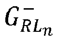
negative memristor 101 is zero (or very low). Conversely, when a negative weighting is set for the nth input and a voltage is applied to the nth row line RLn, a current will flow throughnegative memristor 101 and along the negative -weight column line CL-, but no current (or a very small current) will flow through thepositive memristor 101 and along the positive-weight column line CL+ since the conductance
positive memristor 101 is zero (or very low). Thus, inputs that are assigned positive weights ultimately cause some charge to be subtracted from the integration capacitor Cint (since they generate a current on the positive-weight column line CL+), while inputs that are assigned negative weights ultimately cause some charge to be added to the integration capacitor Cint (since they generate a current on the negative-weight column line CL-). In other words, the expression


- In certain examples, each input of a given MAC may have its associated positive and
negative memristors 101 set independently from thememristors 101 of the other inputs of the same MAC, and therefore in such examples it is possible for one input of a MAC to be assigned a positive weight while another input of the same MAC is assigned a negative weight. - Although in the examples described above positive weightings are associated with subtracting charge from the integration capacitor Cint (e.g., via the first current mirroring circuitry 301) and negative weightings are associated with adding charge to the integration capacitor Cint (e.g., via the second current mirroring circuitry 302), this is merely one example and an opposite convention could be used.
- In certain examples, the example
electronic device 10 illustrated inFig. 5 may include an artificial neural network ("ANN"). For example, thecrossbar array 110, therow driver circuitry 200, and thecolumn output circuits 310, may correspond to a first layer of the ANN. In such an example, each MAC of thecrossbar array 110 may correspond to an induvial neuron. Specifically, each pair of column lines CL+ and CL- may correspond to an individual neuron, and the neuron may include each of thememristors 101 in the corresponding columns together with thecolumn output circuit 310 of the corresponding columns. There may be additional layers of the ANN subsequent to the first layer, in which case the outputY = (y1, y2, ..., yM) of the first layer may be fed to the second layer as an input thereof. - In particular, in certain examples, the output
Y = (y1, y2, ..., yM) of the first layer may be a digital output vector. In such examples, the exampleelectronic device 10 illustrated inFig. 5 may include theoutput circuitry 500, as well as thesecond layer 1000 and its associatedinput stage 2000 as described above and illustrated inFig. 3 . In such examples, theoutput circuitry 500,second layer 1000, andinput stage 2000 may be configured in the same manner described above in relation toFig. 3 , and therefore duplicative description of these features is omitted. - As another example, the output
Y = (y1, y2, ..., yM) of the first layer may be an analog output vector. In such examples, the exampleelectronic device 10 illustrated inFig. 5 may include theoutput circuitry 600, as well as thesecond layer 1001 and its associatedinput stage 2001 as described above and illustrated inFig. 4 . In such examples, theoutput circuitry 600,second layer 1001, andinput stage 2001 may be configured in the same manner described above in relation toFig. 4 , and therefore duplicative description of these features is omitted. -
Fig. 6 illustrates an example method of operating an electronic device. For example, the method may be for operating an artificial neural network that has a first layer comprising a crossbar array (such as thecrossbar array 100 or 110) with row lines, column lines, and memristors that each are connected between one of the row lines and one of the column lines. The example method may be performed, for example, via one or more controllers of the electronic devices, such as, for example, thecontroller 400. - The example method includes applying a plurality of analog voltages to a first node during a plurality of time periods, respectively (see block 6001). For example, voltages V1 - VP may be applied to the first node during time period t1 - tP, respectively, where P ≥ 2.
- The example method may also include, for each of the row lines, selectively connecting the row line to the first node during one of the plurality of time periods based on a digital input vector (see block 6002). For example, for each row line RLn, the row line RLn may be selectively connected to the first node at one of the time periods t1-tP based on digital input xn that corresponds to the row line RLn. In particular, for each row line RLn, the row line RLn may be connected to the first node at the timing tp, where p = xn. Connecting a given row line RLn to the first node in accordance with
block 6002 may result in the voltage Vp being applied to the given row line RLn, since Vp is applied to the first node during tp in accordance withblock 6001. - The example method may also include, for each of the column lines, closing at least one switch corresponding to the column line for a specified amount of time (tint) during each of the plurality of time periods, and, while the at least one switch is closed, causing an integration current to flow to or from an integration capacitor corresponding to the column line whose magnitude mirrors a current flowing on the column line (see block 6003). For example, the at least one switch of each of the column lines may be controlled in the manner described above by applying an integration control signal (such as Ctr_Int) to the switches. Specifically, the integration control signal may be pulsed to an active level during each of the time period t1 - tP with a pulse width equal to the specified amount of time (tint).
- In
block 6003, the causing of the integration current to flow to or from the integration capacitor when the at least one switch is closed may be achieved via a current mirroring circuit (such as the current mirroring circuit 301) that is connected between the column line and the switch. For example, causing the integration current to flow to or from the integration capacitor when the at least one switch is closed may include applying a first voltage (e.g., Vss) to the current mirroring circuit at least while the switch is closed. - The example method may also include generating an output vector for the first layer based on the respective voltages that are stored in the integration capacitors of the column lines after an end of the plurality of time periods (see block 6004).
- In certain examples, the crossbar array may further include second column lines that each correspond to one of the column lines and second memristors that each are connected between one of the row lines and one of the second column lines (such as in the crossbar array 310). In such examples, the method may further include at
block 6003 for each of the column lines: while the at least one switch of the column line is closed, causing a second integration current to flow to or from the integration capacitor of the column line whose magnitude mirrors a current flowing on the one of the second column lines that corresponds to the column line, where the first integration current and the second integration current flow in opposite directions relative to the integration capacitor of the column line. - In certain examples, each neuron of the first layer is associated with one of the column lines and a corresponding one of the second column lines. In such examples, the example method may further comprise: setting a positive weight for a first given input of a given neuron by adjusting a resistance of one of the memristors that is connected to the associated column line, and setting a negative weight for a second given input of the given neuron by adjusting a resistance of one of the memristors that is connected to the associated second column line.
- In certain examples, the output vector for the first layer is a digital output vector. In such examples, generating the output vector for the first layer at
block 6004 may include feeding signals based on the respective voltages stored in the integration capacitors of the column lines after the end of the plurality of time periods to at least one analog-to-digital converter. In certain examples, the signals fed to the at least one analog-to-digital converter may be voltages sampled from the voltages stored in the integration capacitors by sample-and-hold circuits. - In certain examples, the output vector for the first layer is an analog output vector. In such examples, generating the output vector for the first layer at
block 6004 may include feeding signals based on the respective voltages stored in the integration capacitors of the column lines after the end of the plurality of time periods to analog buffer circuitry. In certain examples, the signals fed to the analog buffer circuitry may be voltages sampled from the voltages stored in the integration capacitors by sample-and-hold circuits. - In the art, the term "memristor" may be used in certain contexts in a broad sense and may be used in certain contexts in a narrow sense. In one narrow sense, "memristor" may refer specifically to circuit elements that exhibit a non-linear relationship between electric charge and magnetic flux (or exhibit a relationship between the time integral of current and the time integral of voltage). In the broad sense, "memristor" refers broadly to any non-volatile memory element that is based on changing resistance states and is read by its resistance. Herein and in the appended claims, "memristor" is always used in the broad sense, unless specifically indicated otherwise; specifically, as used herein, "memristor" refers broadly to any non-volatile memory element that is based on changing resistance states and is read by its resistance. Thus, the
memristors 101 may be formed by, for example, a memristor in the narrow sense of the term, a memory element that changes the resistance across a dielectric solid-state material, a phase-change memory element (sometimes referred to as PCM or PCRAM), a conductive-bridging memory element (sometimes referred to as CBRAM or a programmable metallization cell), a magnetoresistive memory element (sometimes referred to as MRAM), or the like. - In addition, in certain examples resistive elements that are not memristors may be used in place of the
memristors 101 to connect the column lines and row lines in thecrossbar array 100. Such resistive elements may be, for example, variable resistance resistors or fixed resistance resistors. Examples of a variable resistance resistor include a transistor operating in liner (ohmic) mode (in which case the channel resistance thereof may be varied by varying a voltage applied to the gate of the transistor), a circuit element that changes its resistance by changing a current path through the circuit element (for example, multiple resistors with different resistances and a switch that selects which of the resistors the current path flows through), and the like. Examples of fixed resistance resistors include poly resistors, laser-trimmed thin films, and the like. Incertain example device 10 in which non-memristor resistive elements are substituted for thememristors 101, the other components of theexample device 10 may be in the same configurations as those described above; in some such examples, additional components specific to the resistive elements may also be added as needed (e.g., gate lines for transistors, control lines for switches, etc.). - In examples in which memristors 101 are used or in which variable resistance resistors are used in place of the
memristors 101, the weights that are assigned to inputs of the MACs may be dynamically adjusted by changing the conductances of thememristors 101 or variable resistance resistors. In examples in which fixed resistance resistors are used in place of the memristors, the weights that are assigned to the inputs of the MACs may be set (e.g., during manufacture) and may thereafter remain fixed. - In an example, an electronic device according to this disclosure comprises:
- a crossbar array comprising row lines, first column lines, second column lines each corresponding to one of the first column lines, and memristors that each are connected between one of the row lines and one of the first column lines or one of the second column lines;
- row driver circuitry to apply a plurality of analog voltages to a first node during a plurality of time periods, respectively, and, for each of the row lines, selectively connect the row line to the first node during one of the plurality of time periods based on a digital input vector; and
- for each of the first column lines, a column output circuit that includes:
- an integration capacitor,
- at least one switch that is controlled by an integration signal,
- first current mirroring circuitry that is to, when the at least one switch is closed, flow a first integration current to or from an electrode of the integration capacitor whose magnitude mirrors a current flowing on the first column line, and second current mirroring circuitry that is to, when the at least one switch is closed, flow a second integration current from or to the electrode whose magnitude mirrors a current flowing on the second column line that corresponds to the first column line, wherein the first current and the second current flow in opposite directions relative to the electrode;
- wherein the integration signal is to close the at least one switch for a specified amount of time during each of the plurality of time periods.
- In an example, for each of the column output circuits, an output signal thereof is based on a voltage difference stored in the integration capacitor after an end of the plurality of time periods.
- In an example, analog-to-digital conversion circuitry to generate a digital output value for each of the column output circuits based on respective voltage differences stored in the integration capacitors of the column output circuits after an end of the plurality of time periods.
- In an example, analog buffer circuitry to output an analog output value for each of the column output circuits based on respective voltage differences stored in the integration capacitors of the column output circuits after an end of the plurality of time periods.
- In an example, the crossbar array, the row driver circuitry, and the column output circuits form a first layer of an artificial neural network, with each neuron of the first layer being associated with one of the first column lines and its corresponding second column line, the electronic device sets a positive weight for a first given input of a given neuron by adjusting a resistance conductance of one of the memristors that is connected to the associated first column line, and the electronic device sets a negative weight for a second given input of the given neuron by adjusting a conductance of one of the memristors that is connected to the associated second column line.
- Throughout this disclosure and in the appended claims, occasionally reference may be made to "a number" of items. Such references to "a number" mean any integer greater than or equal to one. In other words, "a number" means the same thing as "at least one". When "a number" is used in this way, the word describing the item(s) may be written in pluralized form for grammatical consistency, but this does not necessarily mean that multiple items are being referred to. Thus, for example, a phrase such as "a number of processors, wherein the processors ..." could encompass both one processor and multiple processors, notwithstanding the use of the pluralized form.
- The fact that the phrase "a number" may be used in referring to some items should not be interpreted to mean that omission of the phrase "a number" when referring to another item means that the item is necessarily singular or necessarily plural.
- In particular, when items are referred to using the articles "a", "an", and "the" without any explicit indication of singularity or multiplicity, this should be understood to mean that there is "at least one" of the item, unless explicitly stated otherwise. When these articles are used in this way, the word describing the item(s) may be written in singular form for grammatical consistency, but this does not necessarily mean that only one items is being referred to. Thus, for example, a phrase such as "a processor, wherein the processor..." could encompass both one processor and multiple processors, notwithstanding the use of the singular form.
- Occasionally the phrase "and/or" is used herein in conjunction with a list of items. This phrase means that any combination of items in the list-from a single item to all of the items and any permutation in between-may be included. Thus, for example, "A, B, and/or C" may include any one of: {A}, {B}, {C}, {A, B}, {A, C}, {C, B}, and {A, C, B}.
- Various example processes were described above, with reference to various example flow charts. In the description and in the illustrated flow charts, operations are set forth in a particular order for ease of description. However, it should be understood that some or all of the operations could be performed in different orders than those described and that some or all of the operations could be performed concurrently.
- While the above disclosure has been shown and described with reference to the foregoing examples, it should be understood that other forms, details, and implementations may be made without departing from the scope of this disclosure.
Claims (15)
- An electronic device comprising:a crossbar array comprising row lines, column lines, and memristors that each are connected between one of the row lines and one of the column lines;row driver circuitry to apply a plurality of analog voltages to a first node during a plurality of time periods, respectively, and, for each of the row lines, selectively connect the row line to the first node during one of the plurality of time periods based on a digital input vector; andfor each of the column lines, a column output circuit that includes:an integration capacitor,a switch that is controlled by an integration control signal, andcurrent mirroring circuitry that is to, when the switch is closed, flow an integration current to or from an electrode of the integration capacitor whose magnitude mirrors a current flowing on the corresponding column line,wherein the integration control signal is to close the switch for a specified amount of time during each of the plurality of time periods.
- The electronic device of claim 1,
wherein, for each of the column output circuits, an output signal thereof is based on a voltage difference stored in the integration capacitor after an end of the plurality of time periods. - The electronic device of claim 1, further comprising:
analog-to-digital conversion circuitry to generate a digital output value for each of the column output circuits based on respective voltage differences stored in the integration capacitors of the column output circuits after an end of the plurality of time periods. - The electronic device of claim 3, further comprising:
a sample-and-hold circuit for each of the column output circuits, each of the sample-and-hold circuits being connected to the integration capacitor of the corresponding column output circuit to sample a voltage of an electrode of the integration capacitor after the end of the plurality of time periods and feed the sampled voltage to the analog-to-digital conversion circuitry. - The electronic device of claim 3,
wherein the crossbar array, the row driver circuitry, and the column output circuits form a first layer of an artificial neural network, the respective digital output values of the column output circuits form a digital output vector of the first layer, and the digital output vector of the first layer is fed as an input to a second layer of the artificial neural network. - The electronic device of claim 1, further comprising:
analog buffer circuitry to output an analog output value for each of the column output circuits based on respective voltage differences stored in the integration capacitors of the column output circuits after an end of the plurality of time periods. - The electronic device of claim 6,
wherein the crossbar array, the row driver circuitry, and the column output circuits form a first layer of an artificial neural network, the respective analog output values of the column output circuits form an analog output vector of the first layer, and the analog output vector of the first layer is fed as an input to a second layer of the artificial neural network. - The electronic device of claim 1,
wherein the crossbar array, the row driver circuitry, and the column output circuits form a first layer of an artificial neural network, with each of the column lines corresponding to an individual neuron of the artificial neural network. - The electronic device of claim 1,
wherein the row driver circuitry includes:a digital-to-analog converter to apply the plurality of analog voltages to the first node by applying a ramp voltage signal whose voltage changes each of the plurality of time periods to the first node, anda switching circuit for each of the row lines, where each of the switching circuits stores a digital value from the digital input vector and connects the first node to the corresponding row line during one of the plurality of time periods that corresponds to the stored digital value. - A method of operating an artificial neural network that has a first layer comprising a crossbar array with row lines, column lines, and memristors that each are connected between one of the row lines and one of the column lines, the method comprising:applying a plurality of analog voltages to a first node during a plurality of time periods, respectively;for each of the row lines, selectively connecting the row line to the first node during one of the plurality of time periods based on a digital input vector;for each of the column lines, closing at least one switch corresponding to the column line for a specified amount of time during each of the plurality of time periods, and, while the at least one switch is closed, causing an integration current to flow to or from an integration capacitor corresponding to the column line whose magnitude mirrors a current flowing on the column line; andgenerating an output vector for the first layer based on the respective voltage differences that are stored in the integration capacitors of the column lines after an end of the plurality of time periods.
- The method of claim 10,
wherein, for each of the column lines, causing the integration current to flow to or from the integration capacitor of the column line includes applying a first voltage to a mirror circuit while the at least one switch corresponding to the column line is closed, the mirror circuit being connected to the column line and to the at least one switch of the column line. - The method of claim 10,
wherein the crossbar array further includes second column lines that each correspond to one of the column lines and second memristors that each are connected between one of the row lines and one of the second column lines, and- further comprising, for each of the column lines: while the at least one switch of the column line is closed, causing a second integration current to flow to or from the integration capacitor of the column line whose magnitude mirrors a current flowing on the one of the second column lines that corresponds to the column line, where the first integration current and the second integration current flow in opposite directions relative to the integration capacitor of the column line. - The method of claim 12,
wherein each neuron of the first layer is associated with one of the column lines and a corresponding one of the second column lines, and
the method further comprises:setting a positive weight for a first given input of a given neuron by adjusting a conductance of one of the memristors that is connected to the associated column line, andsetting a negative weight for a second given input of the given neuron by adjusting a conductance of one of the memristors that is connected to the associated second column line. - The method of claim 10,
wherein the output vector for the first layer is a digital output vector, and
generating the output vector for the first layer includes feeding signals based on the respective voltage differences stored in the integration capacitors of the column lines after the end of the plurality of time periods to at least one analog-to-digital converter. - The method of claim 10,
wherein the output vector for the first layer is an analog output vector, and
generating the output vector for the first layer includes feeding signals based on the respective voltage differences stored in the integration capacitors of the column lines after the end of the plurality of time periods to analog buffer circuitry.
Applications Claiming Priority (1)
| Application Number | Priority Date | Filing Date | Title |
|---|---|---|---|
| US15/449,071 US11315009B2 (en) | 2017-03-03 | 2017-03-03 | Analog multiplier-accumulators |
Publications (2)
| Publication Number | Publication Date |
|---|---|
| EP3370145A1 EP3370145A1 (en) | 2018-09-05 |
| EP3370145B1 true EP3370145B1 (en) | 2019-10-30 |
Family
ID=61800245
Family Applications (1)
| Application Number | Title | Priority Date | Filing Date |
|---|---|---|---|
| EP18159707.1A Active EP3370145B1 (en) | 2017-03-03 | 2018-03-02 | Analog multiplier-accumulators |
Country Status (5)
| Country | Link |
|---|---|
| US (1) | US11315009B2 (en) |
| EP (1) | EP3370145B1 (en) |
| KR (1) | KR20180101276A (en) |
| CN (1) | CN108536422A (en) |
| TW (1) | TWI657381B (en) |
Families Citing this family (53)
| Publication number | Priority date | Publication date | Assignee | Title |
|---|---|---|---|---|
| US10878317B2 (en) * | 2017-09-11 | 2020-12-29 | Samsung Electronics Co., Ltd. | Method and system for performing analog complex vector-matrix multiplication |
| KR102627117B1 (en) * | 2017-11-17 | 2024-01-23 | 가부시키가이샤 한도오따이 에네루기 켄큐쇼 | Addition method, semiconductor device, and electronic device |
| US10496374B2 (en) * | 2018-03-22 | 2019-12-03 | Hewlett Packard Enterprise Development Lp | Crossbar array operations using ALU modified signals |
| US10418550B2 (en) * | 2018-05-29 | 2019-09-17 | Nanjing University | High temperature resistant memristor based on two-dimensional covalent crystal and preparation method thereof |
| US10452472B1 (en) * | 2018-06-04 | 2019-10-22 | Hewlett Packard Enterprise Development Lp | Tunable and dynamically adjustable error correction for memristor crossbars |
| TWI799588B (en) * | 2018-07-13 | 2023-04-21 | 日商索尼股份有限公司 | Product sum operation device, product sum operation circuit, product sum operation system, and product sum operation method |
| US11410025B2 (en) * | 2018-09-07 | 2022-08-09 | Tetramem Inc. | Implementing a multi-layer neural network using crossbar array |
| WO2020068121A1 (en) * | 2018-09-28 | 2020-04-02 | Hewlett Packard Enterprise Development Lp | Charge metering circuit for memristor |
| US10831860B2 (en) * | 2018-10-11 | 2020-11-10 | International Business Machines Corporation | Alignment techniques to match symmetry point as zero-weight point in analog crosspoint arrays |
| JP6521207B1 (en) * | 2018-11-08 | 2019-05-29 | Tdk株式会社 | Product-sum operation unit, product-sum operation method, logical operation device and neuromorphic device |
| CN109542392A (en) * | 2018-11-09 | 2019-03-29 | 复旦大学 | Low-power consumption weighted sum circuit based on memristor crossed array |
| DE102018219313A1 (en) * | 2018-11-13 | 2020-05-14 | Robert Bosch Gmbh | Method and device for implementing a matrix operation |
| CN109524039B (en) * | 2018-11-21 | 2020-10-09 | 复旦大学 | Structure and related method for expanding resistance state number of memristor |
| US11204740B2 (en) | 2018-12-04 | 2021-12-21 | Electronics And Telecommunications Research Institute | Neuromorphic arithmetic device and operating method thereof |
| CN109740744A (en) * | 2018-12-13 | 2019-05-10 | 南京邮电大学 | Specified element weight operation method based on memristor matrix |
| KR102692218B1 (en) * | 2018-12-19 | 2024-08-05 | 에스케이하이닉스 주식회사 | Neuromorphic system performing supervised training using error back propagation |
| EP3674991B1 (en) * | 2018-12-28 | 2024-07-17 | IMEC vzw | Multibit neural network |
| JP2020126427A (en) * | 2019-02-04 | 2020-08-20 | ソニー株式会社 | Computation device, product-sum operation system, and setting method |
| JP2020126426A (en) * | 2019-02-04 | 2020-08-20 | ソニー株式会社 | Computation device and sum-product operation system |
| US11132176B2 (en) * | 2019-03-20 | 2021-09-28 | Macronix International Co., Ltd. | Non-volatile computing method in flash memory |
| JP2020160887A (en) * | 2019-03-27 | 2020-10-01 | ソニー株式会社 | Computing device and product-sum computing system |
| US20200320373A1 (en) * | 2019-04-03 | 2020-10-08 | Realtek Semiconductor Corp. | Mixed-signal neurons for neuromorphic computing and method thereof |
| GB2583782B (en) | 2019-05-07 | 2021-11-10 | Cirrus Logic Int Semiconductor Ltd | Computing circuitry |
| US20200356847A1 (en) | 2019-05-07 | 2020-11-12 | Hrl Laboratories, Llc | Transistorless all-memristor neuromorphic circuits for in-memory computing |
| US11194886B2 (en) | 2019-05-09 | 2021-12-07 | Applied Materials, Inc. | Bit-ordered binary-weighted multiplier-accumulator |
| CN111985630B (en) * | 2019-05-22 | 2024-07-12 | 力旺电子股份有限公司 | Control circuit applied to product accumulation circuit of neural network-like system |
| CN110209375B (en) * | 2019-05-30 | 2021-03-26 | 浙江大学 | Multiply-accumulate circuit based on radix-4 coding and differential weight storage |
| US12026601B2 (en) | 2019-06-26 | 2024-07-02 | Micron Technology, Inc. | Stacked artificial neural networks |
| TWI770444B (en) * | 2019-07-03 | 2022-07-11 | 財團法人工業技術研究院 | Neural circuit |
| CN112183734A (en) * | 2019-07-03 | 2021-01-05 | 财团法人工业技术研究院 | Neuron circuit |
| CN211653633U (en) * | 2019-07-08 | 2020-10-09 | 神亚科技股份有限公司 | Multiplier device |
| US11735256B2 (en) * | 2019-09-01 | 2023-08-22 | Tetramem Inc. | Reducing disturbance in crossbar array circuits |
| US11573792B2 (en) | 2019-09-03 | 2023-02-07 | Samsung Electronics Co., Ltd. | Method and computing device with a multiplier-accumulator circuit |
| KR20220069966A (en) * | 2019-09-17 | 2022-05-27 | 아나플래시 인코포레이티드 | Multiply-Accumulate Units |
| US11354383B2 (en) * | 2019-09-27 | 2022-06-07 | Applied Materials, Inc | Successive bit-ordered binary-weighted multiplier-accumulator |
| KR102225558B1 (en) * | 2019-10-14 | 2021-03-08 | 연세대학교 산학협력단 | Multilayer Computing Circuit Based on Analog Signal Transfer with On-Chip Activation Function |
| CN110991628B (en) * | 2019-11-02 | 2023-04-18 | 复旦大学 | Neuron circuit based on charge pump |
| JP6818116B1 (en) | 2019-11-22 | 2021-01-20 | ウィンボンド エレクトロニクス コーポレーション | Electronic devices and data processing methods using crossbar arrays |
| CN110795062A (en) * | 2019-11-29 | 2020-02-14 | 珠海复旦创新研究院 | Half adder, full adder and multiplier based on memristor array |
| US11574173B2 (en) * | 2019-12-19 | 2023-02-07 | Qualcomm Incorporated | Power efficient near memory analog multiply-and-accumulate (MAC) |
| KR20210119805A (en) | 2020-03-25 | 2021-10-06 | 삼성전자주식회사 | Neuromorphic device and method of using the same |
| US11562240B2 (en) * | 2020-05-27 | 2023-01-24 | International Business Machines Corporation | Efficient tile mapping for row-by-row convolutional neural network mapping for analog artificial intelligence network inference |
| CN111815640B (en) * | 2020-07-21 | 2022-05-03 | 江苏经贸职业技术学院 | Memristor-based RBF neural network medical image segmentation algorithm |
| KR20220020097A (en) | 2020-08-11 | 2022-02-18 | 삼성전자주식회사 | Processing apparatus and electronic system having the same |
| US11200948B1 (en) * | 2020-08-27 | 2021-12-14 | Hewlett Packard Enterprise Development Lp | System for a flexible conductance crossbar |
| US11488664B2 (en) | 2020-10-13 | 2022-11-01 | International Business Machines Corporation | Distributing device array currents across segment mirrors |
| KR102574426B1 (en) | 2020-12-31 | 2023-09-04 | 한국과학기술원 | Apparatus and method for mac calculation for machine learning algorithm |
| US11705196B2 (en) * | 2021-03-09 | 2023-07-18 | Tetramem Inc. | Auto-calibrating crossbar-based apparatuses |
| CN113285710B (en) * | 2021-06-04 | 2023-01-20 | 广东工业大学 | Memristor cross array-based logic gate circuit and NAND gate and NOR gate implementation method |
| CN116579392A (en) * | 2023-02-21 | 2023-08-11 | 鹏城实验室 | Neural network training operation system and method based on conductance adjustable device |
| CN116029351B (en) * | 2023-03-30 | 2023-06-13 | 南京大学 | Analog domain accumulation reading circuit based on photoelectric calculation unit |
| CN116185338B (en) * | 2023-04-23 | 2023-07-14 | 中国人民解放军国防科技大学 | Multiplier based on memristor |
| US11954586B2 (en) * | 2023-08-04 | 2024-04-09 | Deepx Co., Ltd. | Neural processing unit being operated based on plural clock signals having multi-phases |
Family Cites Families (12)
| Publication number | Priority date | Publication date | Assignee | Title |
|---|---|---|---|---|
| TW279231B (en) | 1995-04-18 | 1996-06-21 | Nat Science Council | This invention is related to a new neural network for prediction |
| TWI417798B (en) | 2008-11-21 | 2013-12-01 | Nat Taipei University Oftechnology | High - speed reverse transfer neural network system with elastic structure and learning function |
| US8856055B2 (en) | 2011-04-08 | 2014-10-07 | International Business Machines Corporation | Reconfigurable and customizable general-purpose circuits for neural networks |
| US9152827B2 (en) | 2012-12-19 | 2015-10-06 | The United States Of America As Represented By The Secretary Of The Air Force | Apparatus for performing matrix vector multiplication approximation using crossbar arrays of resistive memory devices |
| US9715655B2 (en) | 2013-12-18 | 2017-07-25 | The United States Of America As Represented By The Secretary Of The Air Force | Method and apparatus for performing close-loop programming of resistive memory devices in crossbar array based hardware circuits and systems |
| US9489618B2 (en) * | 2014-05-27 | 2016-11-08 | Purdue Research Foudation | Electronic comparison systems |
| CN104978996A (en) | 2015-07-24 | 2015-10-14 | 广东科技学院 | Three-dimensional-structure storer based on memristor |
| US10248907B2 (en) * | 2015-10-20 | 2019-04-02 | International Business Machines Corporation | Resistive processing unit |
| CN105552222B (en) | 2015-12-25 | 2017-02-22 | 中国人民解放军国防科学技术大学 | Cross rod structured memristor based on amorphous-state lanthanum manganate thin film and preparation method of cross rod structured memristor |
| US10664271B2 (en) * | 2016-01-30 | 2020-05-26 | Hewlett Packard Enterprise Development Lp | Dot product engine with negation indicator |
| CN105844330B (en) | 2016-03-22 | 2019-06-28 | 华为技术有限公司 | The data processing method and neural network processor of neural network processor |
| CN106373611A (en) | 2016-09-29 | 2017-02-01 | 华中科技大学 | Storage and calculation array structure and operation method thereof |
-
2017
- 2017-03-03 US US15/449,071 patent/US11315009B2/en active Active
-
2018
- 2018-03-02 TW TW107107040A patent/TWI657381B/en not_active IP Right Cessation
- 2018-03-02 EP EP18159707.1A patent/EP3370145B1/en active Active
- 2018-03-05 CN CN201810179601.1A patent/CN108536422A/en active Pending
- 2018-03-05 KR KR1020180025996A patent/KR20180101276A/en unknown
Non-Patent Citations (1)
| Title |
|---|
| None * |
Also Published As
| Publication number | Publication date |
|---|---|
| US20180253643A1 (en) | 2018-09-06 |
| CN108536422A (en) | 2018-09-14 |
| EP3370145A1 (en) | 2018-09-05 |
| US11315009B2 (en) | 2022-04-26 |
| TW201833824A (en) | 2018-09-16 |
| TWI657381B (en) | 2019-04-21 |
| KR20180101276A (en) | 2018-09-12 |
Similar Documents
| Publication | Publication Date | Title |
|---|---|---|
| EP3370145B1 (en) | Analog multiplier-accumulators | |
| US10534840B1 (en) | Multiplication using non-volatile memory cells | |
| CN111433792B (en) | Counter-based resistance processing unit of programmable resettable artificial neural network | |
| US11948618B2 (en) | Non-volatile analog resistive memory cells implementing ferroelectric select transistors | |
| WO2024109644A1 (en) | Method for operating memristor array, and data processing apparatus | |
| US20210064979A1 (en) | Computing circuitry | |
| WO2024131396A1 (en) | Delay buffer unit and operation method therefor, and calculation apparatus and operation method therefor | |
| US11942144B2 (en) | In-memory computation system with drift compensation circuit | |
| CN114281149B (en) | RRAM array summation operation circuit and method | |
| US20200058352A1 (en) | Crossbar array with reduced disturbance | |
| US9524775B1 (en) | Correlation detector | |
| US10847219B2 (en) | Row switch resistance error reduction for RRAM crossbar array circuit | |
| EP4354443A2 (en) | Calibration methods and structures for partitioned memory architecture with single resistor or dual resistor memory elements | |
| US20240119975A1 (en) | Partitioned memory architecture and method for repeatedly using the architecture for multiple in-memory processing layers | |
| WO2024119839A1 (en) | Fixed asymmetry compensation for multiply and accumulate operations | |
| US11494464B1 (en) | Analog vector-matrix multiplication by capacitive elements with resistive state storage | |
| US20240120001A1 (en) | Partitioned memory architecture with single resistor or dual resistor memory elements for in-memory pipeline processing | |
| US20240120004A1 (en) | Partitioned memory architecture with dual resistor memory elements for in-memory serial processing | |
| US20200134438A1 (en) | Dynamic range and linearity of resistive elements for analog computing |
Legal Events
| Date | Code | Title | Description |
|---|---|---|---|
| PUAI | Public reference made under article 153(3) epc to a published international application that has entered the european phase |
Free format text: ORIGINAL CODE: 0009012 |
|
| STAA | Information on the status of an ep patent application or granted ep patent |
Free format text: STATUS: THE APPLICATION HAS BEEN PUBLISHED |
|
| AK | Designated contracting states |
Kind code of ref document: A1 Designated state(s): AL AT BE BG CH CY CZ DE DK EE ES FI FR GB GR HR HU IE IS IT LI LT LU LV MC MK MT NL NO PL PT RO RS SE SI SK SM TR |
|
| AX | Request for extension of the european patent |
Extension state: BA ME |
|
| RAP1 | Party data changed (applicant data changed or rights of an application transferred) |
Owner name: HEWLETT PACKARD ENTERPRISE DEVELOPMENT LP |
|
| STAA | Information on the status of an ep patent application or granted ep patent |
Free format text: STATUS: REQUEST FOR EXAMINATION WAS MADE |
|
| 17P | Request for examination filed |
Effective date: 20190221 |
|
| RBV | Designated contracting states (corrected) |
Designated state(s): AL AT BE BG CH CY CZ DE DK EE ES FI FR GB GR HR HU IE IS IT LI LT LU LV MC MK MT NL NO PL PT RO RS SE SI SK SM TR |
|
| GRAP | Despatch of communication of intention to grant a patent |
Free format text: ORIGINAL CODE: EPIDOSNIGR1 |
|
| STAA | Information on the status of an ep patent application or granted ep patent |
Free format text: STATUS: GRANT OF PATENT IS INTENDED |
|
| RIC1 | Information provided on ipc code assigned before grant |
Ipc: G06F 7/544 20060101AFI20190611BHEP |
|
| INTG | Intention to grant announced |
Effective date: 20190628 |
|
| GRAS | Grant fee paid |
Free format text: ORIGINAL CODE: EPIDOSNIGR3 |
|
| GRAA | (expected) grant |
Free format text: ORIGINAL CODE: 0009210 |
|
| STAA | Information on the status of an ep patent application or granted ep patent |
Free format text: STATUS: THE PATENT HAS BEEN GRANTED |
|
| AK | Designated contracting states |
Kind code of ref document: B1 Designated state(s): AL AT BE BG CH CY CZ DE DK EE ES FI FR GB GR HR HU IE IS IT LI LT LU LV MC MK MT NL NO PL PT RO RS SE SI SK SM TR |
|
| REG | Reference to a national code |
Ref country code: GB Ref legal event code: FG4D |
|
| REG | Reference to a national code |
Ref country code: CH Ref legal event code: EP |
|
| REG | Reference to a national code |
Ref country code: AT Ref legal event code: REF Ref document number: 1196866 Country of ref document: AT Kind code of ref document: T Effective date: 20191115 |
|
| REG | Reference to a national code |
Ref country code: DE Ref legal event code: R096 Ref document number: 602018001000 Country of ref document: DE |
|
| REG | Reference to a national code |
Ref country code: IE Ref legal event code: FG4D |
|
| REG | Reference to a national code |
Ref country code: LT Ref legal event code: MG4D |
|
| PG25 | Lapsed in a contracting state [announced via postgrant information from national office to epo] |
Ref country code: PT Free format text: LAPSE BECAUSE OF FAILURE TO SUBMIT A TRANSLATION OF THE DESCRIPTION OR TO PAY THE FEE WITHIN THE PRESCRIBED TIME-LIMIT Effective date: 20200302 Ref country code: LV Free format text: LAPSE BECAUSE OF FAILURE TO SUBMIT A TRANSLATION OF THE DESCRIPTION OR TO PAY THE FEE WITHIN THE PRESCRIBED TIME-LIMIT Effective date: 20191030 Ref country code: GR Free format text: LAPSE BECAUSE OF FAILURE TO SUBMIT A TRANSLATION OF THE DESCRIPTION OR TO PAY THE FEE WITHIN THE PRESCRIBED TIME-LIMIT Effective date: 20200131 Ref country code: NO Free format text: LAPSE BECAUSE OF FAILURE TO SUBMIT A TRANSLATION OF THE DESCRIPTION OR TO PAY THE FEE WITHIN THE PRESCRIBED TIME-LIMIT Effective date: 20200130 Ref country code: PL Free format text: LAPSE BECAUSE OF FAILURE TO SUBMIT A TRANSLATION OF THE DESCRIPTION OR TO PAY THE FEE WITHIN THE PRESCRIBED TIME-LIMIT Effective date: 20191030 Ref country code: LT Free format text: LAPSE BECAUSE OF FAILURE TO SUBMIT A TRANSLATION OF THE DESCRIPTION OR TO PAY THE FEE WITHIN THE PRESCRIBED TIME-LIMIT Effective date: 20191030 Ref country code: SE Free format text: LAPSE BECAUSE OF FAILURE TO SUBMIT A TRANSLATION OF THE DESCRIPTION OR TO PAY THE FEE WITHIN THE PRESCRIBED TIME-LIMIT Effective date: 20191030 Ref country code: NL Free format text: LAPSE BECAUSE OF FAILURE TO SUBMIT A TRANSLATION OF THE DESCRIPTION OR TO PAY THE FEE WITHIN THE PRESCRIBED TIME-LIMIT Effective date: 20191030 Ref country code: BG Free format text: LAPSE BECAUSE OF FAILURE TO SUBMIT A TRANSLATION OF THE DESCRIPTION OR TO PAY THE FEE WITHIN THE PRESCRIBED TIME-LIMIT Effective date: 20200130 Ref country code: FI Free format text: LAPSE BECAUSE OF FAILURE TO SUBMIT A TRANSLATION OF THE DESCRIPTION OR TO PAY THE FEE WITHIN THE PRESCRIBED TIME-LIMIT Effective date: 20191030 |
|
| REG | Reference to a national code |
Ref country code: NL Ref legal event code: MP Effective date: 20191030 |
|
| PG25 | Lapsed in a contracting state [announced via postgrant information from national office to epo] |
Ref country code: RS Free format text: LAPSE BECAUSE OF FAILURE TO SUBMIT A TRANSLATION OF THE DESCRIPTION OR TO PAY THE FEE WITHIN THE PRESCRIBED TIME-LIMIT Effective date: 20191030 Ref country code: IS Free format text: LAPSE BECAUSE OF FAILURE TO SUBMIT A TRANSLATION OF THE DESCRIPTION OR TO PAY THE FEE WITHIN THE PRESCRIBED TIME-LIMIT Effective date: 20200229 Ref country code: HR Free format text: LAPSE BECAUSE OF FAILURE TO SUBMIT A TRANSLATION OF THE DESCRIPTION OR TO PAY THE FEE WITHIN THE PRESCRIBED TIME-LIMIT Effective date: 20191030 |
|
| PG25 | Lapsed in a contracting state [announced via postgrant information from national office to epo] |
Ref country code: AL Free format text: LAPSE BECAUSE OF FAILURE TO SUBMIT A TRANSLATION OF THE DESCRIPTION OR TO PAY THE FEE WITHIN THE PRESCRIBED TIME-LIMIT Effective date: 20191030 |
|
| PG25 | Lapsed in a contracting state [announced via postgrant information from national office to epo] |
Ref country code: EE Free format text: LAPSE BECAUSE OF FAILURE TO SUBMIT A TRANSLATION OF THE DESCRIPTION OR TO PAY THE FEE WITHIN THE PRESCRIBED TIME-LIMIT Effective date: 20191030 Ref country code: DK Free format text: LAPSE BECAUSE OF FAILURE TO SUBMIT A TRANSLATION OF THE DESCRIPTION OR TO PAY THE FEE WITHIN THE PRESCRIBED TIME-LIMIT Effective date: 20191030 Ref country code: CZ Free format text: LAPSE BECAUSE OF FAILURE TO SUBMIT A TRANSLATION OF THE DESCRIPTION OR TO PAY THE FEE WITHIN THE PRESCRIBED TIME-LIMIT Effective date: 20191030 Ref country code: RO Free format text: LAPSE BECAUSE OF FAILURE TO SUBMIT A TRANSLATION OF THE DESCRIPTION OR TO PAY THE FEE WITHIN THE PRESCRIBED TIME-LIMIT Effective date: 20191030 Ref country code: ES Free format text: LAPSE BECAUSE OF FAILURE TO SUBMIT A TRANSLATION OF THE DESCRIPTION OR TO PAY THE FEE WITHIN THE PRESCRIBED TIME-LIMIT Effective date: 20191030 |
|
| REG | Reference to a national code |
Ref country code: DE Ref legal event code: R097 Ref document number: 602018001000 Country of ref document: DE |
|
| REG | Reference to a national code |
Ref country code: AT Ref legal event code: MK05 Ref document number: 1196866 Country of ref document: AT Kind code of ref document: T Effective date: 20191030 |
|
| PG25 | Lapsed in a contracting state [announced via postgrant information from national office to epo] |
Ref country code: IT Free format text: LAPSE BECAUSE OF FAILURE TO SUBMIT A TRANSLATION OF THE DESCRIPTION OR TO PAY THE FEE WITHIN THE PRESCRIBED TIME-LIMIT Effective date: 20191030 Ref country code: SM Free format text: LAPSE BECAUSE OF FAILURE TO SUBMIT A TRANSLATION OF THE DESCRIPTION OR TO PAY THE FEE WITHIN THE PRESCRIBED TIME-LIMIT Effective date: 20191030 Ref country code: SK Free format text: LAPSE BECAUSE OF FAILURE TO SUBMIT A TRANSLATION OF THE DESCRIPTION OR TO PAY THE FEE WITHIN THE PRESCRIBED TIME-LIMIT Effective date: 20191030 |
|
| PLBE | No opposition filed within time limit |
Free format text: ORIGINAL CODE: 0009261 |
|
| STAA | Information on the status of an ep patent application or granted ep patent |
Free format text: STATUS: NO OPPOSITION FILED WITHIN TIME LIMIT |
|
| 26N | No opposition filed |
Effective date: 20200731 |
|
| PG25 | Lapsed in a contracting state [announced via postgrant information from national office to epo] |
Ref country code: MC Free format text: LAPSE BECAUSE OF FAILURE TO SUBMIT A TRANSLATION OF THE DESCRIPTION OR TO PAY THE FEE WITHIN THE PRESCRIBED TIME-LIMIT Effective date: 20191030 |
|
| PG25 | Lapsed in a contracting state [announced via postgrant information from national office to epo] |
Ref country code: AT Free format text: LAPSE BECAUSE OF FAILURE TO SUBMIT A TRANSLATION OF THE DESCRIPTION OR TO PAY THE FEE WITHIN THE PRESCRIBED TIME-LIMIT Effective date: 20191030 Ref country code: SI Free format text: LAPSE BECAUSE OF FAILURE TO SUBMIT A TRANSLATION OF THE DESCRIPTION OR TO PAY THE FEE WITHIN THE PRESCRIBED TIME-LIMIT Effective date: 20191030 |
|
| REG | Reference to a national code |
Ref country code: BE Ref legal event code: MM Effective date: 20200331 |
|
| PG25 | Lapsed in a contracting state [announced via postgrant information from national office to epo] |
Ref country code: LU Free format text: LAPSE BECAUSE OF NON-PAYMENT OF DUE FEES Effective date: 20200302 |
|
| PG25 | Lapsed in a contracting state [announced via postgrant information from national office to epo] |
Ref country code: FR Free format text: LAPSE BECAUSE OF NON-PAYMENT OF DUE FEES Effective date: 20200331 Ref country code: IE Free format text: LAPSE BECAUSE OF NON-PAYMENT OF DUE FEES Effective date: 20200302 |
|
| PG25 | Lapsed in a contracting state [announced via postgrant information from national office to epo] |
Ref country code: BE Free format text: LAPSE BECAUSE OF NON-PAYMENT OF DUE FEES Effective date: 20200331 |
|
| REG | Reference to a national code |
Ref country code: CH Ref legal event code: PL |
|
| PG25 | Lapsed in a contracting state [announced via postgrant information from national office to epo] |
Ref country code: CH Free format text: LAPSE BECAUSE OF NON-PAYMENT OF DUE FEES Effective date: 20210331 Ref country code: LI Free format text: LAPSE BECAUSE OF NON-PAYMENT OF DUE FEES Effective date: 20210331 |
|
| PG25 | Lapsed in a contracting state [announced via postgrant information from national office to epo] |
Ref country code: TR Free format text: LAPSE BECAUSE OF FAILURE TO SUBMIT A TRANSLATION OF THE DESCRIPTION OR TO PAY THE FEE WITHIN THE PRESCRIBED TIME-LIMIT Effective date: 20191030 Ref country code: MT Free format text: LAPSE BECAUSE OF FAILURE TO SUBMIT A TRANSLATION OF THE DESCRIPTION OR TO PAY THE FEE WITHIN THE PRESCRIBED TIME-LIMIT Effective date: 20191030 Ref country code: CY Free format text: LAPSE BECAUSE OF FAILURE TO SUBMIT A TRANSLATION OF THE DESCRIPTION OR TO PAY THE FEE WITHIN THE PRESCRIBED TIME-LIMIT Effective date: 20191030 |
|
| PG25 | Lapsed in a contracting state [announced via postgrant information from national office to epo] |
Ref country code: MK Free format text: LAPSE BECAUSE OF FAILURE TO SUBMIT A TRANSLATION OF THE DESCRIPTION OR TO PAY THE FEE WITHIN THE PRESCRIBED TIME-LIMIT Effective date: 20191030 |
|
| REG | Reference to a national code |
Ref country code: DE Ref legal event code: R082 Ref document number: 602018001000 Country of ref document: DE Representative=s name: FLEUCHAUS & GALLO PARTNERSCHAFT MBB - PATENT- , DE Ref country code: DE Ref legal event code: R082 Ref document number: 602018001000 Country of ref document: DE Representative=s name: FLEUCHAUS & GALLO PARTNERSCHAFT MBB PATENTANWA, DE |
|
| PGFP | Annual fee paid to national office [announced via postgrant information from national office to epo] |
Ref country code: DE Payment date: 20240328 Year of fee payment: 7 Ref country code: GB Payment date: 20240319 Year of fee payment: 7 |