EP3365969B1 - Power modules with programmed virtual resistance - Google Patents
Power modules with programmed virtual resistance Download PDFInfo
- Publication number
- EP3365969B1 EP3365969B1 EP16823163.7A EP16823163A EP3365969B1 EP 3365969 B1 EP3365969 B1 EP 3365969B1 EP 16823163 A EP16823163 A EP 16823163A EP 3365969 B1 EP3365969 B1 EP 3365969B1
- Authority
- EP
- European Patent Office
- Prior art keywords
- phase
- power
- voltage
- abc
- command voltage
- Prior art date
- Legal status (The legal status is an assumption and is not a legal conclusion. Google has not performed a legal analysis and makes no representation as to the accuracy of the status listed.)
- Active
Links
Images


Classifications
-
- H—ELECTRICITY
- H02—GENERATION; CONVERSION OR DISTRIBUTION OF ELECTRIC POWER
- H02M—APPARATUS FOR CONVERSION BETWEEN AC AND AC, BETWEEN AC AND DC, OR BETWEEN DC AND DC, AND FOR USE WITH MAINS OR SIMILAR POWER SUPPLY SYSTEMS; CONVERSION OF DC OR AC INPUT POWER INTO SURGE OUTPUT POWER; CONTROL OR REGULATION THEREOF
- H02M1/00—Details of apparatus for conversion
- H02M1/12—Arrangements for reducing harmonics from AC input or output
-
- H—ELECTRICITY
- H02—GENERATION; CONVERSION OR DISTRIBUTION OF ELECTRIC POWER
- H02M—APPARATUS FOR CONVERSION BETWEEN AC AND AC, BETWEEN AC AND DC, OR BETWEEN DC AND DC, AND FOR USE WITH MAINS OR SIMILAR POWER SUPPLY SYSTEMS; CONVERSION OF DC OR AC INPUT POWER INTO SURGE OUTPUT POWER; CONTROL OR REGULATION THEREOF
- H02M1/00—Details of apparatus for conversion
- H02M1/08—Circuits specially adapted for the generation of control voltages for semiconductor devices incorporated in static converters
-
- H—ELECTRICITY
- H02—GENERATION; CONVERSION OR DISTRIBUTION OF ELECTRIC POWER
- H02M—APPARATUS FOR CONVERSION BETWEEN AC AND AC, BETWEEN AC AND DC, OR BETWEEN DC AND DC, AND FOR USE WITH MAINS OR SIMILAR POWER SUPPLY SYSTEMS; CONVERSION OF DC OR AC INPUT POWER INTO SURGE OUTPUT POWER; CONTROL OR REGULATION THEREOF
- H02M7/00—Conversion of AC power input into DC power output; Conversion of DC power input into AC power output
- H02M7/02—Conversion of AC power input into DC power output without possibility of reversal
- H02M7/04—Conversion of AC power input into DC power output without possibility of reversal by static converters
- H02M7/05—Capacitor coupled rectifiers
-
- H—ELECTRICITY
- H02—GENERATION; CONVERSION OR DISTRIBUTION OF ELECTRIC POWER
- H02M—APPARATUS FOR CONVERSION BETWEEN AC AND AC, BETWEEN AC AND DC, OR BETWEEN DC AND DC, AND FOR USE WITH MAINS OR SIMILAR POWER SUPPLY SYSTEMS; CONVERSION OF DC OR AC INPUT POWER INTO SURGE OUTPUT POWER; CONTROL OR REGULATION THEREOF
- H02M7/00—Conversion of AC power input into DC power output; Conversion of DC power input into AC power output
- H02M7/02—Conversion of AC power input into DC power output without possibility of reversal
- H02M7/04—Conversion of AC power input into DC power output without possibility of reversal by static converters
- H02M7/12—Conversion of AC power input into DC power output without possibility of reversal by static converters using discharge tubes with control electrode or semiconductor devices with control electrode
-
- H—ELECTRICITY
- H02—GENERATION; CONVERSION OR DISTRIBUTION OF ELECTRIC POWER
- H02M—APPARATUS FOR CONVERSION BETWEEN AC AND AC, BETWEEN AC AND DC, OR BETWEEN DC AND DC, AND FOR USE WITH MAINS OR SIMILAR POWER SUPPLY SYSTEMS; CONVERSION OF DC OR AC INPUT POWER INTO SURGE OUTPUT POWER; CONTROL OR REGULATION THEREOF
- H02M7/00—Conversion of AC power input into DC power output; Conversion of DC power input into AC power output
- H02M7/42—Conversion of DC power input into AC power output without possibility of reversal
- H02M7/44—Conversion of DC power input into AC power output without possibility of reversal by static converters
- H02M7/48—Conversion of DC power input into AC power output without possibility of reversal by static converters using discharge tubes with control electrode or semiconductor devices with control electrode
- H02M7/493—Conversion of DC power input into AC power output without possibility of reversal by static converters using discharge tubes with control electrode or semiconductor devices with control electrode the static converters being arranged for operation in parallel
-
- H—ELECTRICITY
- H02—GENERATION; CONVERSION OR DISTRIBUTION OF ELECTRIC POWER
- H02M—APPARATUS FOR CONVERSION BETWEEN AC AND AC, BETWEEN AC AND DC, OR BETWEEN DC AND DC, AND FOR USE WITH MAINS OR SIMILAR POWER SUPPLY SYSTEMS; CONVERSION OF DC OR AC INPUT POWER INTO SURGE OUTPUT POWER; CONTROL OR REGULATION THEREOF
- H02M1/00—Details of apparatus for conversion
- H02M1/0003—Details of control, feedback or regulation circuits
- H02M1/0025—Arrangements for modifying reference values, feedback values or error values in the control loop of a converter
-
- H—ELECTRICITY
- H02—GENERATION; CONVERSION OR DISTRIBUTION OF ELECTRIC POWER
- H02M—APPARATUS FOR CONVERSION BETWEEN AC AND AC, BETWEEN AC AND DC, OR BETWEEN DC AND DC, AND FOR USE WITH MAINS OR SIMILAR POWER SUPPLY SYSTEMS; CONVERSION OF DC OR AC INPUT POWER INTO SURGE OUTPUT POWER; CONTROL OR REGULATION THEREOF
- H02M1/00—Details of apparatus for conversion
- H02M1/0048—Circuits or arrangements for reducing losses
-
- Y—GENERAL TAGGING OF NEW TECHNOLOGICAL DEVELOPMENTS; GENERAL TAGGING OF CROSS-SECTIONAL TECHNOLOGIES SPANNING OVER SEVERAL SECTIONS OF THE IPC; TECHNICAL SUBJECTS COVERED BY FORMER USPC CROSS-REFERENCE ART COLLECTIONS [XRACs] AND DIGESTS
- Y02—TECHNOLOGIES OR APPLICATIONS FOR MITIGATION OR ADAPTATION AGAINST CLIMATE CHANGE
- Y02B—CLIMATE CHANGE MITIGATION TECHNOLOGIES RELATED TO BUILDINGS, e.g. HOUSING, HOUSE APPLIANCES OR RELATED END-USER APPLICATIONS
- Y02B70/00—Technologies for an efficient end-user side electric power management and consumption
- Y02B70/10—Technologies improving the efficiency by using switched-mode power supplies [SMPS], i.e. efficient power electronics conversion e.g. power factor correction or reduction of losses in power supplies or efficient standby modes
Definitions
- Embodiments relate to a method, apparatus, and system to increase the apparent resistance of power modules in power converters so as to de-couple the performance of these power converters from bridge losses, bridge errors, and compensation errors, and also to mitigate the effects of transient interactions between and within power converters that are closely coupled to an AC source.
- errors are introduced in the voltage realized at the output due to several factors.
- factors may include a mis-match in dc levels which are induced by the dynamics of a balancing action of the series capacitors in a multi-level design and by lags in the sampling of the dc voltage levels, modulator transition between voltage levels, and dead- time during switching of the power module.
- dead-time compensation is used.
- the dead-time compensation must be guarded against the feasibility of adding dc components.
- the common mode dc components in the system require high resistance to ground in order to prevent circulation of dc components.
- WO 2015/155183 A1 discloses an active damping control of an electrical converter with a resonant output filter.
- WO 2015/108614 A1 discloses modular, multi-channel, interleaved power converters.
- US 2014/160818 discloses systems and methods for controlling an electrical power supply.
- Another relevant prior art is DAHONO P A ED - INSTITUTE OF ELECTRICAL AND ELECTRONICS ENGINEERS, "A control method to damp oscillation in the input Ic filter of ac-dc pwm converters", POWER ELECTRONICS SPECIALISTS CONFERENCE; [ANNUAL POWER ELECTRONICS SPECIALISTS CONFERENCE], (20020623), vol. 4, ISBN 978-0-7803-7262-7, pages 1630 - 1635 .
- Calculating the command voltage may comprise calculating a reference output voltage in a DQ reference frame for the power modules based upon a voltage drop due to a fundamental current across the programmed virtual resistance. Calculating the command voltage may comprise subtracting the product of the programmed virtual resistance and the detected current from the reference output voltage. Calculating the command voltage may comprise adding a bridge drop compensation to the reference output voltage.
- Calculating the command voltage may comprise transforming coordinates of the detected voltage into DQ reference coordinates.
- Calculating the command voltage may comprise: estimating a power line or a rotor angle based on a measurement or estimation using phase locked loop, flux observer and zero crossing detection; and transforming, based on the estimated power line or the rotor angle, the DQ reference coordinate into coordinates of the reference output voltage.
- the present invention provides an apparatus according to claim 5.
- the logic may be configured to calculate the command voltage by calculating a reference output voltage in a DQ reference frame for the power modules based upon a voltage drop due to a fundamental current across the programmed virtual resistance.
- the logic may be configured to calculate the command voltage by subtracting the product of the programmed virtual resistance and the detected current from the reference output voltage.
- the logic may be configured to calculate the command voltage by adding a bridge drop compensation to the reference output voltage.
- the logic may be configured to calculate the command voltage by transforming coordinates of the detected voltage into DQ reference coordinates.
- the logic is configured to calculate the command voltage by: estimating a power line or a rotor angle based on a measurement or estimation using phase locked loop, flux observer and zero crossing detection; and transforming, based on the estimated power line or the rotor angle, the DQ reference coordinate into coordinates of the reference output voltage.
- the at least one power channel may comprise parallel power channels.
- the present invention provides a system according to claims 10 to 13.
- the at least one power channel may comprise parallel power channels.
- a method, apparatus, and system is provided to increase the apparent resistance of power modules of a power converter in a manner which decouples the power converter from bridge losses, bridge errors, and compensation errors, and also to mitigate the effects of transient interactions between and within power converters that are closely coupled to a power source, such as, for example, an AC source.
- a power module refers to the switching element within a power converter that realizes the voltage commanded by the control system.
- a power module is connected to a phase arm and may be arranged into single or multiple parallel power channels to form the power converter.
- FIG. 1 illustrates a circuit diagram of a multi-phase power converter 10, such as, for example, a three-phase converter having a plurality of power modules assembled into a single power channel 11, operatively connected to a power source or motor having phase voltages V ABC and phase currents I ABC which flow to the power channel 11 of the converter 10.
- the power converter 10 may include a sensor 12 or electronic device to detect or measure the phase voltages V ABC and phase currents I ABC may be operatively connected between the power channel 11 and a controller 13 to control the operation of the converter 10 based upon the detected or measured phase voltages V ABC and phase currents I ABC which are received as signals from the sensor 12.
- the controller 13 may be operatively connected to a sensor 12 located outside of the housing of the controller 13.
- the controller 13 may include one or more control blocks 13a-13d.
- control block 13a may, upon a detection (i.e., sensing or estimation) of the voltage V ABC at the terminals and the current I ABC of each phase arm connected to a corresponding power module PM A , PM B , PM C of the power channel 11 (or receive a signal representing the same), transform coordinates of the detected voltage V ABC and the detected current I ABC into DQ reference coordinates.
- Control block 13a may additionally estimate or measure a power line or a rotor angle based on the detection using a phase locked loop (PLL), flux observer, zero crossing detection, or other methods.
- PLL phase locked loop
- Control block 13b may implement DQ regulators compensating for a programmed virtual resistance R mod to calculate the reference output voltage V ref , ABC in the DQ coordinate frame.
- Control block 13c may transform, based on the line or the rotor angle, the DQ reference coordinate into coordinates of the reference output voltage V ref , ABC .
- Control block 13d may then calculate a command voltage V com , ABC to be transmitted to the power modules PM A , PM B , PM C of the power channel 11.
- the calculation of the command voltage V com ABC may be based on a plurality of control factors, such as, for example, the reference output voltage V ref , ABC for each phase arm of the converter 10, a bridge drop compensation BDC ABC based on the detected current I ABC of each phase arm of the power channel 11, and a product of a programmed virtual resistance R mod and the detected current I ABC .
- the programmed virtual resistance R mod module is considered in the control scheme.
- the converter 10 compensates for this resistance as a feed-forward in the DQ reference frame.
- V ref the reference output voltage
- ABC the product of current I ABC and the programmed virtual resistance R mod module is subtracted from the reference output voltage V ref , ABC .
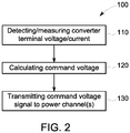
- FIG. 2 illustrates a method 100 of controlling a converter having three-phases in accordance with embodiments.
- the method 100 may be implemented as a set of logic and/or firmware instructions stored in a machine- or computer-readable storage medium such as random access memory (RAM), read only memory (ROM), programmable ROM (PROM), flash memory, etc., in configurable logic such as, for example, programmable logic arrays (PLAs), field programmable gate arrays (FPGAs), complex programmable logic devices (CPLDs), in fixed functionality logic hardware using circuit technology such as, for example, application specific integrated circuit (ASIC), complementary metal oxide semiconductor (CMOS) or transistor-transistor logic (TTL) technology, or any combination thereof.
- PLAs programmable logic arrays
- FPGAs field programmable gate arrays
- CPLDs complex programmable logic devices
- ASIC application specific integrated circuit
- CMOS complementary metal oxide semiconductor
- TTL transistor-transistor logic
- computer program code to carry out operations shown in the method 100 may be written in any combination of one or more programming languages, including an object oriented programming language such as Java, Smalltalk, C++ or the like and conventional procedural programming languages, such as the "C" programming language or similar programming languages.
- object oriented programming language such as Java, Smalltalk, C++ or the like
- conventional procedural programming languages such as the "C" programming language or similar programming languages.
- Illustrated processing block 110 involves detecting or measuring the voltages V ABC and the currents I ABC which flow to each phase arm connected to a corresponding one of power modules PM A , PM B, PM C of the channel 11. Alternatively, the voltages V ABC and the currents I ABC may be estimated.
- Illustrated processing block 120 involves calculating a command voltage V com , ABC based on at least one of a reference output voltage V ref , ABC for each power module PM A , PM B , PMc, a bridge drop compensation BDC ABC based on the detected current I ABC of each power module PM A , PM B , PM C , and a product of a programmed virtual resistance R mod and the detected current I ABC .
- Such a calculation may include, for example, calculating the reference output voltage V ref , ABC in a DQ reference frame for each power module PM A , PM B , PM C while taking into consideration a voltage drop due to a fundamental current across the programmed virtual resistance.
- calculation(s) of processing block 120 for example, may be performed in accordance with at least one of the control blocks 13a-13d noted herein.
- Illustrated processing block 130 involves supplying a command voltage signal to each phase arm of the power converer 10 based on the calculated command voltage V com, ABC .
- FIG. 3 illustrates a circuit diagram of a control scheme for a power converter 200 having a pair of power channels, 210, 220 such as, for example, a three-phase converter 200 having a plurality of power modules assembled into a pair of parallel power channels 210, 220 and operating into a common power source or motor.
- the control scheme involves phase voltages V ABC1 , V ABC2 at the terminals of the power channels 210, 220 terminals and phase currents I ABC1 , I ABC2 which flow to the power modules PM A1 , PM B1 , PM C1 of the first power channel 210 and the power modules PM A2 , PM B2 , PM C2 of the second power channel 220.
- the power converter 200 may include a sensor 211 or device to detect or measure the phase voltages V ABC at the terminal of the power channels 210, 220 and the phase currents I ABC1 , I ABC2 at the phase arm of the power channels 210, 220 may be operatively connected between each power channel 210, 220, and a controller 212 is to control the operation of each power channel 210, 220 based upon the detected or measured phase voltage V ABC and the phase currents I ABC1 , I ABC2 which are received as signals from the sensor 211.
- the controller 212 may be operatively connected to a sensor 211 located outside of the housing of the controller 212.
- the controller 212 may include one or more control blocks 212a-212d.
- control block 212a may, upon a detection of the converter terminal voltage and the current of each phase arm of the power channels 210, 220 (or receive a signal representing the same), transform coordinates of the detected voltage V ABC into DQ reference coordinates.
- Control block 212a may additionally estimate or measure a power line or a rotor angle based on the detection using a phase locked loop (PLL), flux observer, zero crossing detection or other methods.
- PLL phase locked loop
- Control block 212b may implement DQ regulators calculating the DQ references for each of the parallel power channels 210, 220 while compensating for a programmed virtual resistance R mod .
- Control block 212c may transform, based on the line or the rotor angle the DQ 1,2 reference coordinate into coordinates of the reference output voltage V ref, ABC1 , V ref, ABC2 .
- Control blocks 212d 1 , 212d 2 may then calculate a command voltage V com, ABC1 , V com, ABC2 to be transmitted to a respective one of the power channels 210, 220.
- the calculation of the command voltage V com, ABCt , V com, ABC2 may be based on a plurality of control factors, such as, for example, the reference output voltage V ref, ABC , V ref, ABC2 for each phase arm of the power channels 210, 220, a bridge drop compensation BDC ABC1 , BDC ABC2 based on the detected current I ABC1 , I ABC2 of each phase arm of the power channels 210, 220 and a product of a programmed virtual resistance R mod and the detected current I ABC1 , I ABC2 .
- the programmed virtual resistance R mod module is considered in the control scheme.
- the power channels 210, 220 compensate for this resistance as a feed-forward in the DQ reference frame.
- the product of current I ABC1 , I ABC2 and the programmed virtual resistance R mod module is subtracted from the reference output voltage V ref, ABC1 , V ref, ABC2 .
- FIG. 4 illustrates a method 300 of controlling a converter having three-phases in accordance with embodiments.
- the method 300 may be implemented as a set of logic and/or firmware instructions stored in a machine- or computer-readable storage medium such as random access memory (RAM), read only memory (ROM), programmable ROM (PROM), flash memory, etc., in configurable logic such as, for example, programmable logic arrays (PLAs), field programmable gate arrays (FPGAs), complex programmable logic devices (CPLDs), in fixed functionality logic hardware using circuit technology such as, for example, application specific integrated circuit (ASIC), complementary metal oxide semiconductor (CMOS) or transistor-transistor logic (TTL) technology, or any combination thereof.
- PLAs programmable logic arrays
- FPGAs field programmable gate arrays
- CPLDs complex programmable logic devices
- ASIC application specific integrated circuit
- CMOS complementary metal oxide semiconductor
- TTL transistor-transistor logic
- computer program code to carry out operations shown in the method 300 may be written in any combination of one or more programming languages, including an object oriented programming language such as Java, Smalltalk, C++ or the like and conventional procedural programming languages, such as the "C" programming language or similar programming languages.
- object oriented programming language such as Java, Smalltalk, C++ or the like
- conventional procedural programming languages such as the "C" programming language or similar programming languages.
- Illustrated processing block 310 involves detecting or measuring the voltage V ABC and the currents I ABC1 , I ABC2 which flow to each phase arm connected to a corresponding one of power modules PM A , PM B , PM C of the power channels 210, 220. Alternatively, the voltage V ABC and the currents I ABC1 , I ABC2 may be estimated.
- Illustrated processing block 320 involves calculating a command voltage based on at least one of a reference output voltage V ref, ABC1 , V ref, ABC2 for each power module PMA, PM B , PMc, a bridge drop compensation BDC ABC1 .
- BDC ABC2 based on the detected current I ABC1 , I ABC2 of each power module PM A , PM B , PM C , and a product of a programmed virtual resistance R mod and the detected current I ABC1 , I ABC2 .
- Such a calculation may include, for example, calculating the reference output voltage V ref, ABC in a DQ reference frame for each power module PM A1 , PM B1 , PM C1 , PM A2 , PM B2 , PM C2 while taking into consideration a voltage drop due to a fundamental current across the programmed virtual resistance R mod .
- calculation(s) of processing block 320 may be performed in accordance with at least one of the control blocks 212a-212d noted herein.
- Illustrated processing block 212d1, 212d2 involves supplying a command voltage signal to each phase arm of the converter 210, 220 based on the calculated command voltage V com1 , V com2 .
- the virtual resistance would also make the impedance of each converter path for any current deviation much higher than the impedance of the AC source or the motor, thereby reducing effects of transient interactions and resonances and provides damping to these phenomena.
- the method, apparatus, and system in accordance with embodiments sets forth a power converter scheme that establishes an apparent low impedance network for the current (impedance notch) which the converter controller intends to establish. For any current deviating from this intended current due to external or internal phenomena, the power converter will offer a higher resistance equal to the programmed virtual resistance.
- a multi-phase power converter implementation in which a voltage reference for each power module is computed as the voltage reference from the power converter controller minus the product of the sampled instantaneous current flowing through the power module times a constant.
- the constant is set as a parameter in the power converter and communicated to the power module.
- the power converter controller computes the output reference output voltage using dq rotating frame control techniques, but compensates for the voltage drop due to this constant assuming it as purely resistive.
- precise control of currents in d and q frames is attained with zero steady state errors due to the action of the conventional compensators.
- Embodiments are to apply a resistance equation at the instantaneous phase current in each phase, and thus, makes the programmed resistance effective for all components and sequences of the waveform (including dc, negative sequence and all harmonics).
- Coupled may be used herein to refer to any type of relationship, direct or indirect, between the components in question, and may apply to electrical, mechanical, fluid, optical, electromagnetic, electromechanical or other connections.
- first the terms “first,” “second, etc. are used herein only to facilitate discussion, and carry no particular temporal or chronological significance unless otherwise indicated.
Landscapes
- Engineering & Computer Science (AREA)
- Power Engineering (AREA)
- Inverter Devices (AREA)
Description
- Embodiments relate to a method, apparatus, and system to increase the apparent resistance of power modules in power converters so as to de-couple the performance of these power converters from bridge losses, bridge errors, and compensation errors, and also to mitigate the effects of transient interactions between and within power converters that are closely coupled to an AC source.
- In electronic power supply systems having multi-level drive configuration with level balancing action, errors are introduced in the voltage realized at the output due to several factors. Such factors, for example, may include a mis-match in dc levels which are induced by the dynamics of a balancing action of the series capacitors in a multi-level design and by lags in the sampling of the dc voltage levels, modulator transition between voltage levels, and dead- time during switching of the power module.
- To mitigate such dead-time distortion during switching, dead-time compensation is used. The dead-time compensation, however, must be guarded against the feasibility of adding dc components. Moreover, in a transformer-less configuration, operating in solidly grounded electronic power supply systems, the common mode dc components in the system require high resistance to ground in order to prevent circulation of dc components.
-
WO 2015/155183 A1 discloses an active damping control of an electrical converter with a resonant output filter.WO 2015/108614 A1 discloses modular, multi-channel, interleaved power converters.US 2014/160818 discloses systems and methods for controlling an electrical power supply. Another relevant prior art is DAHONO P A ED - INSTITUTE OF ELECTRICAL AND ELECTRONICS ENGINEERS, "A control method to damp oscillation in the input Ic filter of ac-dc pwm converters", POWER ELECTRONICS SPECIALISTS CONFERENCE; [ANNUAL POWER ELECTRONICS SPECIALISTS CONFERENCE], (20020623), vol. 4, ISBN 978-0-7803-7262-7, pages 1630 - 1635. - While the invention is defined in the independent claims, further aspects of the invention are set forth in the dependent claims, the drawings and the following description:
The present invention provides a method according toclaim 1. - Calculating the command voltage may comprise calculating a reference output voltage in a DQ reference frame for the power modules based upon a voltage drop due to a fundamental current across the programmed virtual resistance. Calculating the command voltage may comprise subtracting the product of the programmed virtual resistance and the detected current from the reference output voltage. Calculating the command voltage may comprise adding a bridge drop compensation to the reference output voltage.
- Calculating the command voltage may comprise transforming coordinates of the detected voltage into DQ reference coordinates. Calculating the command voltage may comprise: estimating a power line or a rotor angle based on a measurement or estimation using phase locked loop, flux observer and zero crossing detection; and transforming, based on the estimated power line or the rotor angle, the DQ reference coordinate into coordinates of the reference output voltage.
- The present invention provides an apparatus according to claim 5.
- The logic may be configured to calculate the command voltage by calculating a reference output voltage in a DQ reference frame for the power modules based upon a voltage drop due to a fundamental current across the programmed virtual resistance. The logic may be configured to calculate the command voltage by subtracting the product of the programmed virtual resistance and the detected current from the reference output voltage. The logic may be configured to calculate the command voltage by adding a bridge drop compensation to the reference output voltage.
- The logic may be configured to calculate the command voltage by transforming coordinates of the detected voltage into DQ reference coordinates. The logic is configured to calculate the command voltage by: estimating a power line or a rotor angle based on a measurement or estimation using phase locked loop, flux observer and zero crossing detection; and transforming, based on the estimated power line or the rotor angle, the DQ reference coordinate into coordinates of the reference output voltage.
- The at least one power channel may comprise parallel power channels.
- The present invention provides a system according to
claims 10 to 13. - The at least one power channel may comprise parallel power channels.
- The various advantages of the embodiments will become apparent to one skilled in the art by reading the following specification and appended claims, and by referencing the following drawings, in which:
-
FIG. 1 illustrates a control system for a single power channel power converter arrangement with Power Modules (PM) including virtual resistance effect, in accordance with embodiments. -
FIG. 2 illustrates a flow chart of a method of controlling the power converter arrangement ofFIG. 1 , in accordance with embodiments. -
FIG. 3 illustrates a control system for multi-power channel power converter arrangement with Power Modules (PM) including virtual resistance effect, in accordance with embodiments. -
FIG. 4 illustrates a flow chart of a method of controlling the power converter arrangement ofFIG. 3 , in accordance with embodiments. -
FIGS. 5a and 5b illustrate a graph of a system response of the control scheme, in accordance with embodiments. -
FIGS. 6a and 6b illustrate a graph of a system response of the control scheme, in accordance with embodiments. - In accordance with embodiments, a method, apparatus, and system is provided to increase the apparent resistance of power modules of a power converter in a manner which decouples the power converter from bridge losses, bridge errors, and compensation errors, and also to mitigate the effects of transient interactions between and within power converters that are closely coupled to a power source, such as, for example, an AC source.
- A power module refers to the switching element within a power converter that realizes the voltage commanded by the control system. A power module is connected to a phase arm and may be arranged into single or multiple parallel power channels to form the power converter.
-
FIG. 1 illustrates a circuit diagram of amulti-phase power converter 10, such as, for example, a three-phase converter having a plurality of power modules assembled into asingle power channel 11, operatively connected to a power source or motor having phase voltages VABC and phase currents IABC which flow to thepower channel 11 of theconverter 10. Thepower converter 10 may include asensor 12 or electronic device to detect or measure the phase voltages VABC and phase currents IABC may be operatively connected between thepower channel 11 and acontroller 13 to control the operation of theconverter 10 based upon the detected or measured phase voltages VABC and phase currents IABC which are received as signals from thesensor 12. Alternatively, in accordance with embodiments, thecontroller 13 may be operatively connected to asensor 12 located outside of the housing of thecontroller 13. - As illustrated in
FIG. 1 , in accordance with embodiments, thecontroller 13 may include one ormore control blocks 13a-13d. - For example,
control block 13a may, upon a detection (i.e., sensing or estimation) of the voltage VABC at the terminals and the current IABC of each phase arm connected to a corresponding power module PMA, PMB, PMC of the power channel 11 (or receive a signal representing the same), transform coordinates of the detected voltage VABC and the detected current IABC into DQ reference coordinates.Control block 13a may additionally estimate or measure a power line or a rotor angle based on the detection using a phase locked loop (PLL), flux observer, zero crossing detection, or other methods. -
Control block 13b may implement DQ regulators compensating for a programmed virtual resistance Rmod to calculate the reference output voltage Vref, ABC in the DQ coordinate frame. -
Control block 13c may transform, based on the line or the rotor angle, the DQ reference coordinate into coordinates of the reference output voltage Vref, ABC. -
Control block 13d may then calculate a command voltage Vcom, ABC to be transmitted to the power modules PMA, PMB, PMC of thepower channel 11. The calculation of the command voltage Vcom ABC may be based on a plurality of control factors, such as, for example, the reference output voltage Vref, ABC for each phase arm of theconverter 10, a bridge drop compensation BDCABC based on the detected current IABC of each phase arm of thepower channel 11, and a product of a programmed virtual resistance Rmod and the detected current IABC. In particular, the command voltage Vcom ABC may be calculated using the following formula:
- In accordance with embodiments, the programmed virtual resistance Rmod module is considered in the control scheme. The
converter 10 compensates for this resistance as a feed-forward in the DQ reference frame. Before the reference output voltage Vref, ABC is utilized by the modulators individual phase power modules, the product of current IABC and the programmed virtual resistance Rmod module is subtracted from the reference output voltage Vref, ABC. An advantage that may be realized through embodiments when the sampling frequency is high, which would be the case in converters having high switching frequency and small filters. In converters with low sampling frequency, current prediction techniques may be used to enhance the control scheme in accordance with embodiments. -
FIG. 2 illustrates amethod 100 of controlling a converter having three-phases in accordance with embodiments. Themethod 100 may be implemented as a set of logic and/or firmware instructions stored in a machine- or computer-readable storage medium such as random access memory (RAM), read only memory (ROM), programmable ROM (PROM), flash memory, etc., in configurable logic such as, for example, programmable logic arrays (PLAs), field programmable gate arrays (FPGAs), complex programmable logic devices (CPLDs), in fixed functionality logic hardware using circuit technology such as, for example, application specific integrated circuit (ASIC), complementary metal oxide semiconductor (CMOS) or transistor-transistor logic (TTL) technology, or any combination thereof. For example, computer program code to carry out operations shown in themethod 100 may be written in any combination of one or more programming languages, including an object oriented programming language such as Java, Smalltalk, C++ or the like and conventional procedural programming languages, such as the "C" programming language or similar programming languages. - Illustrated
processing block 110 involves detecting or measuring the voltages VABC and the currents IABC which flow to each phase arm connected to a corresponding one of power modules PMA, PMB, PMC of thechannel 11. Alternatively, the voltages VABC and the currents IABC may be estimated. - Illustrated
processing block 120 involves calculating a command voltage Vcom, ABC based on at least one of a reference output voltage Vref, ABC for each power module PMA, PMB, PMc, a bridge drop compensation BDCABC based on the detected current IABC of each power module PMA, PMB, PMC, and a product of a programmed virtual resistance Rmod and the detected current IABC. Such a calculation may include, for example, calculating the reference output voltage Vref, ABC in a DQ reference frame for each power module PMA, PMB, PMC while taking into consideration a voltage drop due to a fundamental current across the programmed virtual resistance. In accordance with embodiments, calculation(s) ofprocessing block 120, for example, may be performed in accordance with at least one of thecontrol blocks 13a-13d noted herein. - Illustrated
processing block 130 involves supplying a command voltage signal to each phase arm of thepower converer 10 based on the calculated command voltage Vcom, ABC. -
FIG. 3 illustrates a circuit diagram of a control scheme for apower converter 200 having a pair of power channels, 210, 220 such as, for example, a three-phase converter 200 having a plurality of power modules assembled into a pair ofparallel power channels power channels first power channel 210 and the power modules PMA2, PMB2, PMC2 of thesecond power channel 220. - In accordance with embodiments, the
power converter 200 may include asensor 211 or device to detect or measure the phase voltages VABC at the terminal of thepower channels power channels power channel controller 212 is to control the operation of eachpower channel sensor 211. Alternatively, in accordance with embodiments, thecontroller 212 may be operatively connected to asensor 211 located outside of the housing of thecontroller 212. - As illustrated in
FIG. 3 , in accordance with embodiments, thecontroller 212 may include one ormore control blocks 212a-212d. - For example,
control block 212a may, upon a detection of the converter terminal voltage and the current of each phase arm of thepower channels 210, 220 (or receive a signal representing the same), transform coordinates of the detected voltage VABC into DQ reference coordinates.Control block 212a may additionally estimate or measure a power line or a rotor angle based on the detection using a phase locked loop (PLL), flux observer, zero crossing detection or other methods. -
Control block 212b may implement DQ regulators calculating the DQ references for each of theparallel power channels -
Control block 212c may transform, based on the line or the rotor angle the DQ1,2 reference coordinate into coordinates of the reference output voltage Vref, ABC1, Vref, ABC2. - Control blocks 212d1, 212d2 may then calculate a command voltage Vcom, ABC1, Vcom, ABC2 to be transmitted to a respective one of the
power channels power channels power channels respective power channel 

- In accordance with embodiments, the programmed virtual resistance Rmod module is considered in the control scheme. The
power channels -
FIG. 4 illustrates amethod 300 of controlling a converter having three-phases in accordance with embodiments. Themethod 300 may be implemented as a set of logic and/or firmware instructions stored in a machine- or computer-readable storage medium such as random access memory (RAM), read only memory (ROM), programmable ROM (PROM), flash memory, etc., in configurable logic such as, for example, programmable logic arrays (PLAs), field programmable gate arrays (FPGAs), complex programmable logic devices (CPLDs), in fixed functionality logic hardware using circuit technology such as, for example, application specific integrated circuit (ASIC), complementary metal oxide semiconductor (CMOS) or transistor-transistor logic (TTL) technology, or any combination thereof. For example, computer program code to carry out operations shown in themethod 300 may be written in any combination of one or more programming languages, including an object oriented programming language such as Java, Smalltalk, C++ or the like and conventional procedural programming languages, such as the "C" programming language or similar programming languages. - Illustrated
processing block 310 involves detecting or measuring the voltage VABC and the currents IABC1, IABC2 which flow to each phase arm connected to a corresponding one of power modules PMA, PMB, PMC of thepower channels - Illustrated
processing block 320 involves calculating a command voltage based on at least one of a reference output voltage Vref, ABC1, Vref, ABC2 for each power module PMA, PMB, PMc, a bridge drop compensation BDCABC1. BDCABC2 based on the detected current IABC1, IABC2 of each power module PMA, PMB, PMC, and a product of a programmed virtual resistance Rmod and the detected current IABC1, IABC2. Such a calculation may include, for example, calculating the reference output voltage Vref, ABC in a DQ reference frame for each power module PMA1, PMB1, PMC1, PMA2, PMB2, PMC2 while taking into consideration a voltage drop due to a fundamental current across the programmed virtual resistance Rmod. In accordance with embodiments, calculation(s) ofprocessing block 320, for example, may be performed in accordance with at least one of thecontrol blocks 212a-212d noted herein. - Illustrated processing block 212d1, 212d2 involves supplying a command voltage signal to each phase arm of the
converter - As illustrated in
FIGS. 5(a) and 5(b) and6(a) and 6(b) , the graphs qualitatively illustrate the influence of this scheme when the programmed virtual resistance is 100% (100% resistance limits the current to 100% when 100% system voltage is applied). - As illustrated in
FIG. 5(a) , for a 0.5% 5th harmonic component in the bridge voltage output due to dead-time voltage loss, a 5% (at fundamental frequency) filter impedance will result in an harmonic current circulation of .5%/(5 X 5%) = 2%. With the virtual resistance, the harmonic current would be limited to 0.5% (FIG. 5(b) ). - As illustrated in
FIG. 6(a) , for a sudden transient deviation in power line voltage by 10%, the prospective current deviation would be more than 10%/5% = 200 % if the DQ controller does not do any action, but with the virtual resistance, the current deviation would be naturally limited to about 2% (FIG. 6(b) . - For power converters with parallel power channels operating into an AC source or a motor, the virtual resistance would also make the impedance of each converter path for any current deviation much higher than the impedance of the AC source or the motor, thereby reducing effects of transient interactions and resonances and provides damping to these phenomena.
- The method, apparatus, and system in accordance with embodiments sets forth a power converter scheme that establishes an apparent low impedance network for the current (impedance notch) which the converter controller intends to establish. For any current deviating from this intended current due to external or internal phenomena, the power converter will offer a higher resistance equal to the programmed virtual resistance.
- In accordance with embodiments, a multi-phase power converter implementation is provided in which a voltage reference for each power module is computed as the voltage reference from the power converter controller minus the product of the sampled instantaneous current flowing through the power module times a constant. The constant is set as a parameter in the power converter and communicated to the power module. The power converter controller computes the output reference output voltage using dq rotating frame control techniques, but compensates for the voltage drop due to this constant assuming it as purely resistive. In addition, precise control of currents in d and q frames is attained with zero steady state errors due to the action of the conventional compensators.
- Embodiments are to apply a resistance equation at the instantaneous phase current in each phase, and thus, makes the programmed resistance effective for all components and sequences of the waveform (including dc, negative sequence and all harmonics).
- The term "coupled" or "connected" may be used herein to refer to any type of relationship, direct or indirect, between the components in question, and may apply to electrical, mechanical, fluid, optical, electromagnetic, electromechanical or other connections. In addition, the terms "first," "second, etc. are used herein only to facilitate discussion, and carry no particular temporal or chronological significance unless otherwise indicated.
- This written description uses examples to disclose the invention, including the preferred embodiments, and also to enable any person skilled in the art to practice the invention, including making and using any devices or systems and performing any incorporated methods. The patentable scope of embodiments is defined by the claims, and may include other examples that occur to those skilled in the art. Such other examples are intended to be within the scope of the claims if they have structural elements that do not differ from the literal language of the claims, or if they include equivalent structural elements with insubstantial differences from the literal languages of the claims. Aspects from the various embodiments described, as well as other known equivalents for each such aspects, may be mixed and matched by one of ordinary skill in the art to construct additional embodiments and techniques in accordance with principles of this application.
Claims (14)
- A method (100; 300) of controlling a multi-phase converter (10; 200) arranged to convert between multi-phase power (VABC, IABC) and DC power and having at least one power channel (11; 210, 220) with a plurality of power modules (PMA, PMB, PMC; PMA1, PMB1, PMC1, PMA2, PMB2, PMC2) connected to respective phase arms, the method (100; 300) comprising:detecting (110; 310) the multi-phase voltage (VABC) and the multi-phase current (IABC) of the power modules (PMA, PMB, PMC; PMA1, PMB1, PMC1, PMA2, PMB2, PMC2);calculating (120; 320) a multi-phase command voltage (Vcom,ABC) based on a product of a programmed virtual resistance (Rmod) and the detected current, wherein calculating (120; 220) the multi-phase command voltage comprises calculating a reference multi-phase voltage (Vref,ABC) in a DQ reference frame for the power modules (PMA, PMB, PMC; PMA1, PMB1, PMC1, PMA2, PMB2, PMC2) compensated for a voltage drop due to a fundamental current across the programmed virtual resistance and subtracting the product of the programmed virtual resistance and the detected current from the reference multi-phase voltage; andtransmitting (130; 330) a multi-phase command voltage signal to the power modules (PMA, PMB, PMC; PMA1, PMB1, PMC1, PMA2, PMB2, PMC2) based on the calculated multi-phase command voltage.
- A method according to claim 1, wherein calculating the multi-phase command voltage comprises adding a bridge drop compensation (BDCABC) to the reference multi-phase voltage.
- A method according to any preceding claim, wherein calculating the multi-phase command voltage comprises transforming coordinates of the detected multi-phase voltage into DQ reference coordinates.
- A method according to claim 3, wherein calculating the multi-phase command voltage comprises:estimating a power line or a rotor angle based on a measurement or estimation using phase locked loop, flux observer and zero crossing detection; andtransforming, based on the estimated power line or the rotor angle, the DQ reference coordinate into coordinates of the reference multi-phase voltage.
- An apparatus (13; 212) for controlling a multi-phase converter (10; 200) arranged to convert between multi-phase power (VABC, IABC) and DC power and having at least one power channel (11; 210, 220) with a plurality of power modules (PMA, PMB, PMC; PMA1, PMB1, PMC1, PMA2, PMB2, PMC2) connected to corresponding phase arms, the apparatus comprising:
logic, at least partially comprising hardware configured to:detect the multi-phase voltage (VABC) and the multi-phase current (IABC) of the power modules (PMA, PMB, PMC; PMA1, PMB1, PMC1, PMA2, PMB2, PMC2);calculate a multi-phase command voltage (Vcom,ABC) based on a product of a programmed virtual resistance (Rmod) and the detected current, wherein the logic is configured to calculate (120; 220) the multi-phase command voltage by calculating a reference multi-phase voltage (Vref,ABC) in a DQ reference frame for the power modules (PMA, PMB, PMC; PMA1, PMB1, PMC1, PMA2, PMB2, PMC2) compensated for a voltage drop due to a fundamental current across the programmed virtual resistance and subtracting the product of the programmed virtual resistance and the detected current from the reference multi-phase voltage; andtransmit a multi-phase command voltage signal to the power modules (PMA, PMB, PMC; PMA1, PMB1, PMC1, PMA2, PMB2, PMC2) based on the calculated multi-phase command voltage. - An apparatus according to claim 5, wherein the logic is configured to calculate the multi-phase command voltage by adding a bridge drop compensation (BDCABC) to the reference multi-phase voltage.
- An apparatus according to claim 5, wherein the logic is configured to calculate the multi-phase command voltage by transforming coordinates of the detected multi-phase voltage into DQ reference coordinates.
- An apparatus according to claim 7, wherein the logic is configured to calculate the multi-phase command voltage by:estimating a power line or a rotor angle based on a measurement or estimation using phase locked loop, flux observer and zero crossing detection; andtransforming, based on the estimated power line or the rotor angle, the DQ reference coordinate into coordinates of the reference multi-phase voltage.
- An apparatus according to any of claims 5 to 8, wherein the at least one power channel comprises parallel power channels.
- A system, comprising:a multi-phase converter (10; 200) arranged to convert multi-phase power (VABC, IABC) into DC output power and having at least one power channel (11; 210, 220) with a plurality of power modules (PMA, PMB, PMC; PMA1, PMB1, PMC1, PMA2, PMB2, PMC2) connected to corresponding phase arms; anda controller (13; 212) formed by the apparatus of claim 5 to control operation of the multi-phase converter (10; 200).
- A system according to claim 10, wherein the hardware is configured to calculate the multi-phase command voltage by adding a bridge drop compensation to the reference multi-phase voltage.
- A system according to claim 10, wherein the hardware is configured to calculate the multi-phase command voltage by transforming coordinates of the detected multi-phase voltage into DQ reference coordinates.
- A system according to claim 12, wherein the hardware is configured to calculate the multi-phase command voltage by:estimating a power line or a rotor angle based on a measurement or estimation using phase locked loop, flux observer and zero crossing detection; andtransforming, based on the estimated power line or the rotor angle, the DQ reference coordinate into coordinates of the reference multi-phase voltage.
- A system according to any of claims 10 to 13, wherein the at least one power channel comprises parallel power channels.
Applications Claiming Priority (2)
| Application Number | Priority Date | Filing Date | Title |
|---|---|---|---|
| US14/945,450 US10439507B2 (en) | 2015-11-19 | 2015-11-19 | Power modules with programmed virtual resistance |
| PCT/EP2016/078129 WO2017085250A1 (en) | 2015-11-19 | 2016-11-18 | Power modules with programmed virtual resistance |
Publications (2)
| Publication Number | Publication Date |
|---|---|
| EP3365969A1 EP3365969A1 (en) | 2018-08-29 |
| EP3365969B1 true EP3365969B1 (en) | 2019-08-14 |
Family
ID=57758558
Family Applications (1)
| Application Number | Title | Priority Date | Filing Date |
|---|---|---|---|
| EP16823163.7A Active EP3365969B1 (en) | 2015-11-19 | 2016-11-18 | Power modules with programmed virtual resistance |
Country Status (4)
| Country | Link |
|---|---|
| US (1) | US10439507B2 (en) |
| EP (1) | EP3365969B1 (en) |
| DK (1) | DK3365969T3 (en) |
| WO (1) | WO2017085250A1 (en) |
Cited By (1)
| Publication number | Priority date | Publication date | Assignee | Title |
|---|---|---|---|---|
| WO2024017472A1 (en) * | 2022-07-20 | 2024-01-25 | Huawei Digital Power Technologies Co., Ltd. | Control entity and method for controlling a converter circuit to imitate an electrical output characteristic of a synchronous machine |
Families Citing this family (5)
| Publication number | Priority date | Publication date | Assignee | Title |
|---|---|---|---|---|
| WO2016134319A1 (en) * | 2015-02-19 | 2016-08-25 | Enphase Energy, Inc. | Method and apparatus for time-domain droop control with integrated phasor current control |
| JP6796029B2 (en) * | 2017-06-13 | 2020-12-02 | 株式会社日立製作所 | New energy source integrated power converter |
| US10536069B2 (en) | 2018-06-15 | 2020-01-14 | Ford Global Technologies, Llc | Virtual resistance gate driver |
| US11177660B2 (en) * | 2020-01-27 | 2021-11-16 | Mitsubishi Electric Power Products, Inc. | System and method for power converter control for virtual impedance |
| CN113472006B (en) * | 2021-06-08 | 2022-10-28 | 浙江工业大学 | Off-grid control method for multi-machine parallel energy storage power converter under complex load |
Citations (1)
| Publication number | Priority date | Publication date | Assignee | Title |
|---|---|---|---|---|
| US20120063179A1 (en) * | 2011-04-05 | 2012-03-15 | Maozhong Gong | System and method for damping lc circuits in power conversion systems |
Family Cites Families (15)
| Publication number | Priority date | Publication date | Assignee | Title |
|---|---|---|---|---|
| JP3945762B2 (en) * | 2002-07-31 | 2007-07-18 | 本田技研工業株式会社 | Structure of door opening and closing device |
| US20040201283A1 (en) | 2003-04-10 | 2004-10-14 | Delta Electronics, Inc. | Parallel power supply system and control method thereof |
| JP2008005632A (en) * | 2006-06-22 | 2008-01-10 | Matsushita Electric Ind Co Ltd | Motor drive device, motor drive method, and disk drive device |
| JP4416764B2 (en) * | 2006-06-29 | 2010-02-17 | 株式会社日立製作所 | Vector controller and inverter module for permanent magnet motor |
| KR101550755B1 (en) * | 2011-07-08 | 2015-09-08 | 카와사키 주코교 카부시키 카이샤 | Power conversion apparatus directed to combined-cycle power generation system |
| JP5820287B2 (en) * | 2012-01-31 | 2015-11-24 | ルネサスエレクトロニクス株式会社 | Motor drive control device and operation method thereof |
| KR101677784B1 (en) * | 2012-09-05 | 2016-11-18 | 엘에스산전 주식회사 | Regenarative inverter device and inverter device using power cell unit |
| US9722511B2 (en) | 2012-12-07 | 2017-08-01 | General Electric Company | Systems and methods for controlling an electrical power supply |
| JP6084863B2 (en) * | 2013-02-28 | 2017-02-22 | 川崎重工業株式会社 | Power converter for grid connection |
| US10826322B2 (en) * | 2013-06-14 | 2020-11-03 | Abb Schweiz Ag | Systems and methods for grid interactive UPS |
| WO2015108614A1 (en) | 2014-01-15 | 2015-07-23 | Abb Technology Ag | Modular, multi-channel, interleaved power converters |
| US11063531B2 (en) * | 2014-02-14 | 2021-07-13 | Wisconsin Alumni Research Foundation | Series connected DC input inverters |
| WO2015155183A1 (en) | 2014-04-09 | 2015-10-15 | Abb Technology Ag | Active damping control of an electrical converter with a resonant output filter |
| US9614461B2 (en) * | 2014-12-02 | 2017-04-04 | Princeton Power Systems, Inc. | Bidirectional high frequency variable speed drive for CHP (combined heating and power) and flywheel applications |
| WO2016134319A1 (en) * | 2015-02-19 | 2016-08-25 | Enphase Energy, Inc. | Method and apparatus for time-domain droop control with integrated phasor current control |
-
2015
- 2015-11-19 US US14/945,450 patent/US10439507B2/en active Active
-
2016
- 2016-11-18 EP EP16823163.7A patent/EP3365969B1/en active Active
- 2016-11-18 DK DK16823163T patent/DK3365969T3/en active
- 2016-11-18 WO PCT/EP2016/078129 patent/WO2017085250A1/en active Application Filing
Patent Citations (1)
| Publication number | Priority date | Publication date | Assignee | Title |
|---|---|---|---|---|
| US20120063179A1 (en) * | 2011-04-05 | 2012-03-15 | Maozhong Gong | System and method for damping lc circuits in power conversion systems |
Cited By (1)
| Publication number | Priority date | Publication date | Assignee | Title |
|---|---|---|---|---|
| WO2024017472A1 (en) * | 2022-07-20 | 2024-01-25 | Huawei Digital Power Technologies Co., Ltd. | Control entity and method for controlling a converter circuit to imitate an electrical output characteristic of a synchronous machine |
Also Published As
| Publication number | Publication date |
|---|---|
| WO2017085250A1 (en) | 2017-05-26 |
| US10439507B2 (en) | 2019-10-08 |
| DK3365969T3 (en) | 2019-11-11 |
| US20170149350A1 (en) | 2017-05-25 |
| EP3365969A1 (en) | 2018-08-29 |
Similar Documents
| Publication | Publication Date | Title |
|---|---|---|
| EP3365969B1 (en) | Power modules with programmed virtual resistance | |
| CA2838384C (en) | Paralleling of active filters with independent controls | |
| CN101355317B (en) | Power converter and power unit | |
| EP1092981B1 (en) | Apparatus and method for measuring current | |
| KR100934311B1 (en) | Inverter device | |
| EP3035511B1 (en) | Method for damping resonant component of common-mode current of multi-phase power converter | |
| CN113678360B (en) | Power conversion device and power generation system | |
| EP1049241A2 (en) | Modified space vector pulse width modulation technique to reduce DC bus ripple effect in voltage source inverters | |
| KR101639192B1 (en) | Apparatus for compensating reactive power | |
| EP3514931A1 (en) | Control device for active filter | |
| US20230261561A1 (en) | Mitigation of harmonic disturbances in a power converter | |
| KR20200001300A (en) | System for controlling grid-connected apparatus for distributed generation | |
| TWI418809B (en) | Isolation operation detection method for mains voltage control type electric energy converter | |
| JP2002335632A (en) | System linkage inverter | |
| CN105940312B (en) | Find out the method and load of the supply voltage of load | |
| KR101736531B1 (en) | Apparatus for restarting medium-voltage inverter | |
| CN113039696A (en) | Power conversion device | |
| KR20210065617A (en) | Controller for active power filter | |
| KR101696510B1 (en) | Inverter controlling system for compensating distortion of output voltage | |
| JP2015046985A (en) | Power converter | |
| JP2014107962A (en) | Harmonic wave suppression device | |
| RU2524347C2 (en) | Device for earth fault current compensation in three-phase electrical networks (versions) | |
| JP2001352764A (en) | Inverter controller | |
| KR101388398B1 (en) | State estimator based voltage control method and apparatus of an inverter with output lc filter for application to uninterruptable power supply | |
| JPH10145973A (en) | Control of active filter for electric power |
Legal Events
| Date | Code | Title | Description |
|---|---|---|---|
| STAA | Information on the status of an ep patent application or granted ep patent |
Free format text: STATUS: UNKNOWN |
|
| STAA | Information on the status of an ep patent application or granted ep patent |
Free format text: STATUS: THE INTERNATIONAL PUBLICATION HAS BEEN MADE |
|
| PUAI | Public reference made under article 153(3) epc to a published international application that has entered the european phase |
Free format text: ORIGINAL CODE: 0009012 |
|
| STAA | Information on the status of an ep patent application or granted ep patent |
Free format text: STATUS: REQUEST FOR EXAMINATION WAS MADE |
|
| 17P | Request for examination filed |
Effective date: 20180523 |
|
| AK | Designated contracting states |
Kind code of ref document: A1 Designated state(s): AL AT BE BG CH CY CZ DE DK EE ES FI FR GB GR HR HU IE IS IT LI LT LU LV MC MK MT NL NO PL PT RO RS SE SI SK SM TR |
|
| AX | Request for extension of the european patent |
Extension state: BA ME |
|
| DAV | Request for validation of the european patent (deleted) | ||
| DAX | Request for extension of the european patent (deleted) | ||
| GRAP | Despatch of communication of intention to grant a patent |
Free format text: ORIGINAL CODE: EPIDOSNIGR1 |
|
| STAA | Information on the status of an ep patent application or granted ep patent |
Free format text: STATUS: GRANT OF PATENT IS INTENDED |
|
| INTG | Intention to grant announced |
Effective date: 20190307 |
|
| GRAS | Grant fee paid |
Free format text: ORIGINAL CODE: EPIDOSNIGR3 |
|
| GRAA | (expected) grant |
Free format text: ORIGINAL CODE: 0009210 |
|
| STAA | Information on the status of an ep patent application or granted ep patent |
Free format text: STATUS: THE PATENT HAS BEEN GRANTED |
|
| AK | Designated contracting states |
Kind code of ref document: B1 Designated state(s): AL AT BE BG CH CY CZ DE DK EE ES FI FR GB GR HR HU IE IS IT LI LT LU LV MC MK MT NL NO PL PT RO RS SE SI SK SM TR |
|
| REG | Reference to a national code |
Ref country code: GB Ref legal event code: FG4D |
|
| REG | Reference to a national code |
Ref country code: CH Ref legal event code: EP Ref country code: AT Ref legal event code: REF Ref document number: 1168193 Country of ref document: AT Kind code of ref document: T Effective date: 20190815 |
|
| REG | Reference to a national code |
Ref country code: DE Ref legal event code: R096 Ref document number: 602016018792 Country of ref document: DE |
|
| REG | Reference to a national code |
Ref country code: IE Ref legal event code: FG4D |
|
| REG | Reference to a national code |
Ref country code: DK Ref legal event code: T3 Effective date: 20191106 |
|
| REG | Reference to a national code |
Ref country code: NL Ref legal event code: MP Effective date: 20190814 |
|
| REG | Reference to a national code |
Ref country code: LT Ref legal event code: MG4D |
|
| PG25 | Lapsed in a contracting state [announced via postgrant information from national office to epo] |
Ref country code: LT Free format text: LAPSE BECAUSE OF FAILURE TO SUBMIT A TRANSLATION OF THE DESCRIPTION OR TO PAY THE FEE WITHIN THE PRESCRIBED TIME-LIMIT Effective date: 20190814 Ref country code: FI Free format text: LAPSE BECAUSE OF FAILURE TO SUBMIT A TRANSLATION OF THE DESCRIPTION OR TO PAY THE FEE WITHIN THE PRESCRIBED TIME-LIMIT Effective date: 20190814 Ref country code: NL Free format text: LAPSE BECAUSE OF FAILURE TO SUBMIT A TRANSLATION OF THE DESCRIPTION OR TO PAY THE FEE WITHIN THE PRESCRIBED TIME-LIMIT Effective date: 20190814 Ref country code: SE Free format text: LAPSE BECAUSE OF FAILURE TO SUBMIT A TRANSLATION OF THE DESCRIPTION OR TO PAY THE FEE WITHIN THE PRESCRIBED TIME-LIMIT Effective date: 20190814 Ref country code: HR Free format text: LAPSE BECAUSE OF FAILURE TO SUBMIT A TRANSLATION OF THE DESCRIPTION OR TO PAY THE FEE WITHIN THE PRESCRIBED TIME-LIMIT Effective date: 20190814 Ref country code: PT Free format text: LAPSE BECAUSE OF FAILURE TO SUBMIT A TRANSLATION OF THE DESCRIPTION OR TO PAY THE FEE WITHIN THE PRESCRIBED TIME-LIMIT Effective date: 20191216 Ref country code: BG Free format text: LAPSE BECAUSE OF FAILURE TO SUBMIT A TRANSLATION OF THE DESCRIPTION OR TO PAY THE FEE WITHIN THE PRESCRIBED TIME-LIMIT Effective date: 20191114 Ref country code: NO Free format text: LAPSE BECAUSE OF FAILURE TO SUBMIT A TRANSLATION OF THE DESCRIPTION OR TO PAY THE FEE WITHIN THE PRESCRIBED TIME-LIMIT Effective date: 20191114 |
|
| REG | Reference to a national code |
Ref country code: AT Ref legal event code: MK05 Ref document number: 1168193 Country of ref document: AT Kind code of ref document: T Effective date: 20190814 |
|
| PG25 | Lapsed in a contracting state [announced via postgrant information from national office to epo] |
Ref country code: IS Free format text: LAPSE BECAUSE OF FAILURE TO SUBMIT A TRANSLATION OF THE DESCRIPTION OR TO PAY THE FEE WITHIN THE PRESCRIBED TIME-LIMIT Effective date: 20191214 Ref country code: ES Free format text: LAPSE BECAUSE OF FAILURE TO SUBMIT A TRANSLATION OF THE DESCRIPTION OR TO PAY THE FEE WITHIN THE PRESCRIBED TIME-LIMIT Effective date: 20190814 Ref country code: AL Free format text: LAPSE BECAUSE OF FAILURE TO SUBMIT A TRANSLATION OF THE DESCRIPTION OR TO PAY THE FEE WITHIN THE PRESCRIBED TIME-LIMIT Effective date: 20190814 Ref country code: LV Free format text: LAPSE BECAUSE OF FAILURE TO SUBMIT A TRANSLATION OF THE DESCRIPTION OR TO PAY THE FEE WITHIN THE PRESCRIBED TIME-LIMIT Effective date: 20190814 Ref country code: GR Free format text: LAPSE BECAUSE OF FAILURE TO SUBMIT A TRANSLATION OF THE DESCRIPTION OR TO PAY THE FEE WITHIN THE PRESCRIBED TIME-LIMIT Effective date: 20191115 Ref country code: RS Free format text: LAPSE BECAUSE OF FAILURE TO SUBMIT A TRANSLATION OF THE DESCRIPTION OR TO PAY THE FEE WITHIN THE PRESCRIBED TIME-LIMIT Effective date: 20190814 |
|
| PG25 | Lapsed in a contracting state [announced via postgrant information from national office to epo] |
Ref country code: TR Free format text: LAPSE BECAUSE OF FAILURE TO SUBMIT A TRANSLATION OF THE DESCRIPTION OR TO PAY THE FEE WITHIN THE PRESCRIBED TIME-LIMIT Effective date: 20190814 |
|
| PG25 | Lapsed in a contracting state [announced via postgrant information from national office to epo] |
Ref country code: AT Free format text: LAPSE BECAUSE OF FAILURE TO SUBMIT A TRANSLATION OF THE DESCRIPTION OR TO PAY THE FEE WITHIN THE PRESCRIBED TIME-LIMIT Effective date: 20190814 Ref country code: EE Free format text: LAPSE BECAUSE OF FAILURE TO SUBMIT A TRANSLATION OF THE DESCRIPTION OR TO PAY THE FEE WITHIN THE PRESCRIBED TIME-LIMIT Effective date: 20190814 Ref country code: PL Free format text: LAPSE BECAUSE OF FAILURE TO SUBMIT A TRANSLATION OF THE DESCRIPTION OR TO PAY THE FEE WITHIN THE PRESCRIBED TIME-LIMIT Effective date: 20190814 Ref country code: RO Free format text: LAPSE BECAUSE OF FAILURE TO SUBMIT A TRANSLATION OF THE DESCRIPTION OR TO PAY THE FEE WITHIN THE PRESCRIBED TIME-LIMIT Effective date: 20190814 Ref country code: IT Free format text: LAPSE BECAUSE OF FAILURE TO SUBMIT A TRANSLATION OF THE DESCRIPTION OR TO PAY THE FEE WITHIN THE PRESCRIBED TIME-LIMIT Effective date: 20190814 |
|
| PG25 | Lapsed in a contracting state [announced via postgrant information from national office to epo] |
Ref country code: SM Free format text: LAPSE BECAUSE OF FAILURE TO SUBMIT A TRANSLATION OF THE DESCRIPTION OR TO PAY THE FEE WITHIN THE PRESCRIBED TIME-LIMIT Effective date: 20190814 Ref country code: IS Free format text: LAPSE BECAUSE OF FAILURE TO SUBMIT A TRANSLATION OF THE DESCRIPTION OR TO PAY THE FEE WITHIN THE PRESCRIBED TIME-LIMIT Effective date: 20200224 Ref country code: SK Free format text: LAPSE BECAUSE OF FAILURE TO SUBMIT A TRANSLATION OF THE DESCRIPTION OR TO PAY THE FEE WITHIN THE PRESCRIBED TIME-LIMIT Effective date: 20190814 Ref country code: CZ Free format text: LAPSE BECAUSE OF FAILURE TO SUBMIT A TRANSLATION OF THE DESCRIPTION OR TO PAY THE FEE WITHIN THE PRESCRIBED TIME-LIMIT Effective date: 20190814 |
|
| REG | Reference to a national code |
Ref country code: DE Ref legal event code: R097 Ref document number: 602016018792 Country of ref document: DE |
|
| REG | Reference to a national code |
Ref country code: CH Ref legal event code: PL |
|
| PLBE | No opposition filed within time limit |
Free format text: ORIGINAL CODE: 0009261 |
|
| STAA | Information on the status of an ep patent application or granted ep patent |
Free format text: STATUS: NO OPPOSITION FILED WITHIN TIME LIMIT |
|
| PG2D | Information on lapse in contracting state deleted |
Ref country code: IS |
|
| PG25 | Lapsed in a contracting state [announced via postgrant information from national office to epo] |
Ref country code: MC Free format text: LAPSE BECAUSE OF FAILURE TO SUBMIT A TRANSLATION OF THE DESCRIPTION OR TO PAY THE FEE WITHIN THE PRESCRIBED TIME-LIMIT Effective date: 20190814 Ref country code: LU Free format text: LAPSE BECAUSE OF NON-PAYMENT OF DUE FEES Effective date: 20191118 Ref country code: LI Free format text: LAPSE BECAUSE OF NON-PAYMENT OF DUE FEES Effective date: 20191130 Ref country code: CH Free format text: LAPSE BECAUSE OF NON-PAYMENT OF DUE FEES Effective date: 20191130 |
|
| 26N | No opposition filed |
Effective date: 20200603 |
|
| REG | Reference to a national code |
Ref country code: BE Ref legal event code: MM Effective date: 20191130 |
|
| PG25 | Lapsed in a contracting state [announced via postgrant information from national office to epo] |
Ref country code: SI Free format text: LAPSE BECAUSE OF FAILURE TO SUBMIT A TRANSLATION OF THE DESCRIPTION OR TO PAY THE FEE WITHIN THE PRESCRIBED TIME-LIMIT Effective date: 20190814 |
|
| PG25 | Lapsed in a contracting state [announced via postgrant information from national office to epo] |
Ref country code: IE Free format text: LAPSE BECAUSE OF NON-PAYMENT OF DUE FEES Effective date: 20191118 |
|
| PG25 | Lapsed in a contracting state [announced via postgrant information from national office to epo] |
Ref country code: BE Free format text: LAPSE BECAUSE OF NON-PAYMENT OF DUE FEES Effective date: 20191130 |
|
| PG25 | Lapsed in a contracting state [announced via postgrant information from national office to epo] |
Ref country code: CY Free format text: LAPSE BECAUSE OF FAILURE TO SUBMIT A TRANSLATION OF THE DESCRIPTION OR TO PAY THE FEE WITHIN THE PRESCRIBED TIME-LIMIT Effective date: 20190814 |
|
| PG25 | Lapsed in a contracting state [announced via postgrant information from national office to epo] |
Ref country code: HU Free format text: LAPSE BECAUSE OF FAILURE TO SUBMIT A TRANSLATION OF THE DESCRIPTION OR TO PAY THE FEE WITHIN THE PRESCRIBED TIME-LIMIT; INVALID AB INITIO Effective date: 20161118 Ref country code: MT Free format text: LAPSE BECAUSE OF FAILURE TO SUBMIT A TRANSLATION OF THE DESCRIPTION OR TO PAY THE FEE WITHIN THE PRESCRIBED TIME-LIMIT Effective date: 20190814 |
|
| PG25 | Lapsed in a contracting state [announced via postgrant information from national office to epo] |
Ref country code: MK Free format text: LAPSE BECAUSE OF FAILURE TO SUBMIT A TRANSLATION OF THE DESCRIPTION OR TO PAY THE FEE WITHIN THE PRESCRIBED TIME-LIMIT Effective date: 20190814 |
|
| PGFP | Annual fee paid to national office [announced via postgrant information from national office to epo] |
Ref country code: DE Payment date: 20241022 Year of fee payment: 9 |
|
| PGFP | Annual fee paid to national office [announced via postgrant information from national office to epo] |
Ref country code: DK Payment date: 20241022 Year of fee payment: 9 |
|
| PGFP | Annual fee paid to national office [announced via postgrant information from national office to epo] |
Ref country code: GB Payment date: 20241023 Year of fee payment: 9 |
|
| PGFP | Annual fee paid to national office [announced via postgrant information from national office to epo] |
Ref country code: FR Payment date: 20241022 Year of fee payment: 9 |