EP3365917B1 - Thermoelectric generator - Google Patents
Thermoelectric generator Download PDFInfo
- Publication number
- EP3365917B1 EP3365917B1 EP16836234.1A EP16836234A EP3365917B1 EP 3365917 B1 EP3365917 B1 EP 3365917B1 EP 16836234 A EP16836234 A EP 16836234A EP 3365917 B1 EP3365917 B1 EP 3365917B1
- Authority
- EP
- European Patent Office
- Prior art keywords
- silicon wafer
- base
- thermoelectric generator
- cone
- union
- Prior art date
- Legal status (The legal status is an assumption and is not a legal conclusion. Google has not performed a legal analysis and makes no representation as to the accuracy of the status listed.)
- Active
Links
Images




Classifications
-
- H—ELECTRICITY
- H10—SEMICONDUCTOR DEVICES; ELECTRIC SOLID-STATE DEVICES NOT OTHERWISE PROVIDED FOR
- H10N—ELECTRIC SOLID-STATE DEVICES NOT OTHERWISE PROVIDED FOR
- H10N10/00—Thermoelectric devices comprising a junction of dissimilar materials, i.e. devices exhibiting Seebeck or Peltier effects
- H10N10/10—Thermoelectric devices comprising a junction of dissimilar materials, i.e. devices exhibiting Seebeck or Peltier effects operating with only the Peltier or Seebeck effects
- H10N10/17—Thermoelectric devices comprising a junction of dissimilar materials, i.e. devices exhibiting Seebeck or Peltier effects operating with only the Peltier or Seebeck effects characterised by the structure or configuration of the cell or thermocouple forming the device
-
- H—ELECTRICITY
- H01—ELECTRIC ELEMENTS
- H01R—ELECTRICALLY-CONDUCTIVE CONNECTIONS; STRUCTURAL ASSOCIATIONS OF A PLURALITY OF MUTUALLY-INSULATED ELECTRICAL CONNECTING ELEMENTS; COUPLING DEVICES; CURRENT COLLECTORS
- H01R13/00—Details of coupling devices of the kinds covered by groups H01R12/70 or H01R24/00 - H01R33/00
- H01R13/73—Means for mounting coupling parts to apparatus or structures, e.g. to a wall
-
- H—ELECTRICITY
- H10—SEMICONDUCTOR DEVICES; ELECTRIC SOLID-STATE DEVICES NOT OTHERWISE PROVIDED FOR
- H10N—ELECTRIC SOLID-STATE DEVICES NOT OTHERWISE PROVIDED FOR
- H10N10/00—Thermoelectric devices comprising a junction of dissimilar materials, i.e. devices exhibiting Seebeck or Peltier effects
- H10N10/01—Manufacture or treatment
-
- H—ELECTRICITY
- H10—SEMICONDUCTOR DEVICES; ELECTRIC SOLID-STATE DEVICES NOT OTHERWISE PROVIDED FOR
- H10N—ELECTRIC SOLID-STATE DEVICES NOT OTHERWISE PROVIDED FOR
- H10N10/00—Thermoelectric devices comprising a junction of dissimilar materials, i.e. devices exhibiting Seebeck or Peltier effects
- H10N10/10—Thermoelectric devices comprising a junction of dissimilar materials, i.e. devices exhibiting Seebeck or Peltier effects operating with only the Peltier or Seebeck effects
- H10N10/13—Thermoelectric devices comprising a junction of dissimilar materials, i.e. devices exhibiting Seebeck or Peltier effects operating with only the Peltier or Seebeck effects characterised by the heat-exchanging means at the junction
-
- H—ELECTRICITY
- H10—SEMICONDUCTOR DEVICES; ELECTRIC SOLID-STATE DEVICES NOT OTHERWISE PROVIDED FOR
- H10N—ELECTRIC SOLID-STATE DEVICES NOT OTHERWISE PROVIDED FOR
- H10N10/00—Thermoelectric devices comprising a junction of dissimilar materials, i.e. devices exhibiting Seebeck or Peltier effects
- H10N10/80—Constructional details
- H10N10/85—Thermoelectric active materials
- H10N10/851—Thermoelectric active materials comprising inorganic compositions
- H10N10/855—Thermoelectric active materials comprising inorganic compositions comprising compounds containing boron, carbon, oxygen or nitrogen
-
- H—ELECTRICITY
- H10—SEMICONDUCTOR DEVICES; ELECTRIC SOLID-STATE DEVICES NOT OTHERWISE PROVIDED FOR
- H10N—ELECTRIC SOLID-STATE DEVICES NOT OTHERWISE PROVIDED FOR
- H10N10/00—Thermoelectric devices comprising a junction of dissimilar materials, i.e. devices exhibiting Seebeck or Peltier effects
- H10N10/80—Constructional details
- H10N10/85—Thermoelectric active materials
- H10N10/851—Thermoelectric active materials comprising inorganic compositions
- H10N10/8556—Thermoelectric active materials comprising inorganic compositions comprising compounds containing germanium or silicon
-
- H—ELECTRICITY
- H10—SEMICONDUCTOR DEVICES; ELECTRIC SOLID-STATE DEVICES NOT OTHERWISE PROVIDED FOR
- H10N—ELECTRIC SOLID-STATE DEVICES NOT OTHERWISE PROVIDED FOR
- H10N19/00—Integrated devices, or assemblies of multiple devices, comprising at least one thermoelectric or thermomagnetic element covered by groups H10N10/00 - H10N15/00
-
- H—ELECTRICITY
- H10—SEMICONDUCTOR DEVICES; ELECTRIC SOLID-STATE DEVICES NOT OTHERWISE PROVIDED FOR
- H10W—GENERIC PACKAGES, INTERCONNECTIONS, CONNECTORS OR OTHER CONSTRUCTIONAL DETAILS OF DEVICES COVERED BY CLASS H10
- H10W90/00—Package configurations
- H10W90/701—Package configurations characterised by the relative positions of pads or connectors relative to package parts
- H10W90/721—Package configurations characterised by the relative positions of pads or connectors relative to package parts of bump connectors
- H10W90/724—Package configurations characterised by the relative positions of pads or connectors relative to package parts of bump connectors between a chip and a stacked insulating package substrate, interposer or RDL
Definitions
- the present invention relates to a thermoelectric generator.
- thermoelectric generator based on a thermoelectric material in the form of a thin film and realized with a microelectronic technology, that may be fabricated through planar processes and correlated techniques of 3D heterogeneous or hybrid integration.
- thermoelectric generator is a device that allows to transform thermal energy into electric energy, thanks to the possibility of exploiting the effect known as Seebeck effect.
- thermoelectric generators The functioning of most of prior art thermoelectric generators is based on the use of a thermoelectric material with a high merit factor ZT, such as bismute telluride and alloys thereof.
- thermoelectric generators are expensive and hardly suitable for mass production.
- thermoelectric generators it is not possible to realize thermoelectric generators on a large scale or to satisfy big markets (automotive, consumer electronics) thus hardly in line with development trends such as Internet of Things or Wearable electronics.
- thermoelectric generators In the last decades, thus, attention has been paid to the possibility of realizing miniaturized thermoelectric generators, using process technologies that are typical for MEMS devices, CMOS devices and more in general for ICs.
- Thermoelectric generators are composed of a set of thermocouples.
- thermocouple is composed of two electrical conducting materials or, as an alternative, to a p-doped semiconductor and a n-doped semiconductor joined together by means of a connection with a high electrical conductivity, typically realized through a metal.
- Thermocouples are generally connected electrically in series and thermally in parallel for obtaining a voltage sufficient for powering an electronic device.
- thermocouple may be either in-plane or out-of-plane, depending on whether the heat flux flowing throughout a thermocouple is in parallel to or orthogonal with the plane in which electric current flows.
- thermoelectric generators the thermocouples of which are in an in-plane configuration
- Figure 1 that depicts the configuration of the publication of Y. Van Andel et al.
- Figure 1 that depicts the configuration of the publication of Y. Van Andel et al.
- thermoelectric generator the thermocouples of which are in an in-plane configuration in respect to a thermoelectric generator the thermocouples of which are in an out-of-plane configuration
- area occupation is larger and as a consequence there is a miniaturization loss.
- larger areas imply a greater production cost of the thermoelectric generator.
- thermoelectric generators in an in-plane configuration are disclosed in the following pubblications:
- thermoelectric generators in an out-of-plane configuration are disclosed in the following publications:
- thermoelectric generator Referring to the miniaturized thermoelectric generator mentioned in the publication by Bottner et al. and shown in figure 2 , this miniaturized thermoelectric generator is obtained by means of a flip chip bonding technique. Nevertheless, the used materials are of known type, i.e. bismute telluride and alloys thereof, and are deposited onto silicon wafer by sputtering.
- thermoelectric generator Referring to the thermoelectric generator mentioned in the publication by Strasser et al. and shown in figure 3 , this thermoelectric generator is realized by surface micromachining.
- thermoelectric generator is composed of two thermoelectric couples realized by BiCMOS technology.
- thermoelectric couples Isolation between the hot part and the cold part of said thermoelectric couples is realized by means of an oxide barrier LOCOS (Local Oxidation of Silicon).
- LOCOS Low Oxidation of Silicon
- thermoelectric material is a layer with a thickness of 400nm in polysilicon partially doped with phosphorous for realizing n-type parts and partially doped with boron for realizing p-type parts.
- thermoelectric generator Referring to the thermoelectric generator mentioned in the publication by Su et al. and shown in figure 4 , this thermoelectric generator is composed of thermocouples realized in p-type and n-type poly-SiGe, connected among them with aluminum.
- thermocouples of said thermoelectric generator are free standing.
- thermoelectric material is substantially shaped as a bridge, because the underlying material has been removed for increasing the temperature difference on the terminals of the thermoelectric material.
- thermoelectric generator The lower part and the upper part of said thermoelectric generator are sealed together by means of the flip-chip bonding technique and by means of an adhesive paste.
- US 2014/0246066 A1 discloses a wafer scale thermoelectric energy harvester and is another example of an out-of plane configuration.
- An object of the present invention is to overcome said drawbacks, providing a thermoelectric generator of compact size, having a simple structure that is configured for increasing the conversion efficiency of thermal energy into electric energy, so as it is possible to transform into electric current also as amount of heat per unit surface greater than thin film prior art devices.
- thermoelectric generator according the enclosed claims, that are integral part of the present description.
- thermoelectric generator according to the invention.
- thermoelectric generator 100 Said part of the thermoelectric generator 100 comprises:
- FIG 5 two base elements 130 are shown, in the bottom substrate 110, with connections 140, better disclosed in detail hereinafter (see figures 9, 10 , 11 ). Between the bottom and top substrates there is an air or vacuum gap 150.
- the structure of the bottom substrate 110 is illustrated. It has a surface 111 with hills 111C and valleys 111V alternated one another.
- the structure of the top substrate 120 is shown. It has a surface 121 with hills 121C and valleys 121V alternated one another.
- Said first substrate 110 and said second substrate 120 are facing one another so as each hill 111C of the first substrate 110 is facing to a respective hill 121C of said second substrate 120 and so as each valley 111V of the first substrate 110 is facing a respective valley 121V of the second substrate 120, as it is clear in figure 5 .
- the respective hills of both layers are in contact through their peak.
- the valleys 111V of the first substrate 1 and the valleys 121V of the second substrate 2 contribute to increase the thermal resistance of air present in the gap between said substrates.
- each of said substrates is composed of a respective silicon wafer.
- first layer 114 of electrically isolating material for example silicon oxide or silicon nitride with a thickness that may range from few nanometers to one micron, in contact with the silicon wafer.
- a localized layer 115 of electrically isolating material for example silicon oxide, silicon nitride
- the thickness of this localized layer 115 ranges from 1 micron up to hundreds of microns, preferably in the order of tens of microns when the thermoelectric material (illustrated hereinafter) is in the order of hundreds of nanometers.
- a truncated-pyramidal shape with any base shape is imparted, for example a rectangular or square base (in the shown examples), or a truncated-conic shape by means of standard photo-lithographic techniques.
- the geometry of the material in this zone and its thermal characteristics are such to make a significantly greater thermal resistance than that of the other parts that constitute the base element (the hill material should be electrically isolating and from a thermal point of view it should have a thermal conductivity as low as possible in respect to that of the thermoelectric material).
- thermoelectric material 116 of p-type or of n-type. This thermoelectric material is deposited onto all side faces (or onto only two faces only) of the truncated-pyramidal or truncated-conical structure 115 (see figure 7 ). The thickness may range between 10 and 1000nm, but it could be even greater than 1 micron depending on the particular application for which the TEG is designed. Examples of TE materials are heavily doped semiconductors such as Si or SiGe.
- the first substrate 110 and the second substrate 120 may be thinned or ultra-thinned crystalline silicon wafers, for carrying greater flux of heat towards the terminals of the thermoelectric material.
- metals 117 extending between about one half of a valley and the beginning of a hill, above the first isolating layer 114, are deposited. There is still another metal 118 at the top of the hill 111C above the thermoelectric material 116. All these metals are electric contacts. The base of the metal 118 that rests on the peak of the hill of the truncated-pyramidal or truncated-conical structure is also a thermal contact.
- the base element 130 of the bottom layer 110 is shown in figure 7 in a perspective view.
- a metal 119 that may be considered an extension of the metal 117 and that surrounds the peak of the hill, is shown.
- the electric contacts 118 and 119 between said metal contacts superposed to the thin film of thermoelectric material may be fixed through a multilayer interface comprising a film of silicide belonging to the group composed of TiSi2, WSi2, MoSi2, PtSi2 and CoSi2, for reducing the electric contact resistance.
- the same metal contacts may be fixed through a multilayer interface comprising an intermediate film of a refractory metal belonging to the group composed of W, Ti, Ta and a film of Titanium nitride in contact with the metal.
- a first layer 124 of an electrically isolating material for example silicon oxide or silicon nitride with a thickness that may range between few nanometers and one micron, in contact with the silicon wafer.
- An electric contact 128 is deposited onto the isolating layer 124, at the peak of the hill 121C.
- the silicon wafers mentioned above may be micro-machined, joined together by means of a smart-cut processing or of the technique Smart StackingTM by Soitec for transferring layers.
- bottom chip bottom chip, figure 6(a)
- bottom chip bottom chip, figure 6(a)
- thermoelectric generator having the maximum temperature difference at the terminals of the thermoelectric material ( ⁇ T effettivo ) an air gap or a gap under vacuum is exploited, in order to allow a better thermal decoupling between the bottom substrate and the top substrate, instead of the oxide layer LOCOS disclosed in the document by Strasser et al.
- the base elements are of n-type when a thermoelectric material constituted by a heavily doped (for example with boron) semiconductor (for example silicon) in which the majority carriers are composed of electrons and of p-type when a thermoelectric material (for example silicon) composed of a heavily doped semiconductor (for example with phosphorous) in which the majority carriers are holes.
- a thermoelectric material constituted by a heavily doped (for example with boron) semiconductor (for example silicon) in which the majority carriers are composed of electrons
- a thermoelectric material for example silicon
- a heavily doped semiconductor for example with phosphorous
- Another possible embodiment of the proposed invention contemplates a base block of the bottom layer 230 with a truncated-pyramidal hill 211C, the deposition of the thermoelectric material 216 on two side faces only of the truncated pyramid, and the side 217 and upper 218 electric contacts as shown in figure 12 .
- thermoelectric generator In order to obtain a thermoelectric generator starting from the base element shown in figure 5 , it is necessary to connect a plurality of base elements of p-type and of n-type as shown hereinbefore.
- figure 13 depicts the grid type connection 2000G among base elements 230P of p-type and 230N of n-type.
- the building blocks are joined by alternating, in the current flux, p-type elements and n-type elements.
- the union by alignment of the building blocks is carried out according to a chip-on-chip mode, chip-on-wafer, wafer-on-wafer; or according to a chip-on-wafer-on-substrate or chip-on-chip-on-substrate mode.
- VIAS interconnection VIAS
- the presence of VIAS constitutes a synergy with the rest of the above disclosed geometry. Indeed, there is a better heat sinking, because heat must follow a path; it shall not go in the substrate but it shall cross it and be sunk beyond the silicon substrate. Moreover in these VIAS electric energy flows therethrough at the same time.
- the VIAS are preferably realized in a thinned wafer.
- the thermal generator, object of the invention allows to maximize the temperature difference on the terminals of the generator.
- a second advantage is given by the fact that there are not inside the thermoelectric generator, object of the invention, suspended structures or bridge structures, differently from prior art thermoelectric generators (such as for example those disclosed in the publication by Strasser et al. and in the publication by Su, Leonov et al.). From a mechanical point of view, said suspended structures or bridge structures weaken the structure of the thermoelectric generator and/or make said thermoelectric generator unsuitable to resist to high temperatures (greater than 60°C) and/or to be sealed by means of specific types of bonding, such as for example flip-chip bonding or metal-to-metal bonding.
- the absence of suspended structure or bridge structures makes the thermal generator, object of the invention, more robust from a mechanical point of view.
- the structure can be miniaturized and directly integrated in the traditional electronic devices, or directly onto silicon or in heterogeneous integrations.
- the base elements in more complex architectures in order to respond to specific application requirements, by placing the base elements electrically in series and/or in parallel in function of the electric amounts that it is desired to obtain at the output. It is possible for example to modify within a certain range the output electrical amounts of the generators by working on the series-parallel electrical interconnections among base elements: for example, if n base elements are all placed electrically in series, the greatest deliverable voltage and the greatest electric resistance (series of n unitary resistances) will be obtained; if the n base elements are placed in parallel, a generator with the minimum resistance (parallel of n unitary resistances) will be obtained; series-parallel connections allow to obtain an electric response that may be modulated between the two ends, either fully in series or fully in parallel.
Landscapes
- Chemical & Material Sciences (AREA)
- Inorganic Chemistry (AREA)
- Engineering & Computer Science (AREA)
- Manufacturing & Machinery (AREA)
- Micromachines (AREA)
- Measuring Temperature Or Quantity Of Heat (AREA)
- Permanent Magnet Type Synchronous Machine (AREA)
Description
- The present invention relates to a thermoelectric generator.
- More in particular, the invention relates to the structure of a thermoelectric generator, based on a thermoelectric material in the form of a thin film and realized with a microelectronic technology, that may be fabricated through planar processes and correlated techniques of 3D heterogeneous or hybrid integration.
- A thermoelectric generator is a device that allows to transform thermal energy into electric energy, thanks to the possibility of exploiting the effect known as Seebeck effect.
- The functioning of most of prior art thermoelectric generators is based on the use of a thermoelectric material with a high merit factor ZT, such as bismute telluride and alloys thereof.
- Nevertheless, bismuth telluride and alloys thereof are scarcely available in nature and as a consequence thermoelectric generators are expensive and hardly suitable for mass production.
- Moreover, these materials cannot be easily scaled down because they are incompatible with manufacturing processes used in microelectronic manufacturing industries.
- As a consequence, it is not possible to realize thermoelectric generators on a large scale or to satisfy big markets (automotive, consumer electronics) thus hardly in line with development trends such as Internet of Things or Wearable electronics.
- In the last decades, thus, attention has been paid to the possibility of realizing miniaturized thermoelectric generators, using process technologies that are typical for MEMS devices, CMOS devices and more in general for ICs.
- Thermoelectric generators are composed of a set of thermocouples.
- A thermocouple is composed of two electrical conducting materials or, as an alternative, to a p-doped semiconductor and a n-doped semiconductor joined together by means of a connection with a high electrical conductivity, typically realized through a metal. Thermocouples are generally connected electrically in series and thermally in parallel for obtaining a voltage sufficient for powering an electronic device.
- A configuration of a thermocouple may be either in-plane or out-of-plane, depending on whether the heat flux flowing throughout a thermocouple is in parallel to or orthogonal with the plane in which electric current flows.
- From a point of view, the fabrication processes of thermoelectric generators, the thermocouples of which are in an in-plane configuration (see
Figure 1 that depicts the configuration of the publication of Y. Van Andel et al.), are simpler than fabrication processes of thermoelectric generators the thermocouples of which are in an out-of-plane configuration. - From another point of view, a drawback of a thermoelectric generator the thermocouples of which are in an in-plane configuration in respect to a thermoelectric generator the thermocouples of which are in an out-of-plane configuration, is that area occupation is larger and as a consequence there is a miniaturization loss. In the industry of microelectronics, generally, larger areas imply a greater production cost of the thermoelectric generator.
- Examples of miniaturized thermoelectric generators in an in-plane configuration are disclosed in the following pubblications:
- Y. Van Andel, M. Jambunathan, R.J.M. Vullers, V. Leonov, Membrane-less in-plane bulk-micromachined thermopiles for energy harvesting, Microelectronic Engineering, Vol. 87 (2010) 1294-1296;
- Xie, J.; Lee, C.; Feng, H. Design, fabrication and characterization of CMOS MEMS-based thermoelectric power generators. J. Micromech. Syst. 2010, 19, 317-324;
- Kao, P.-H.; Shih, P.-J.; Dai, C.-L.; Liu, M.-C. Fabrication and characterization of CMOS-MEMS thermoelectric micro generators. ;
- Wang, Z.; Van Andel, Y.; Jambunathan, M.; Leonov, V.; Elfrink, R.; Vullers, J.M. Characterization of a bulk-micromachined membraneless in-plane thermopile. J. Electron. Mater. 2011, 40, 499-503.13;
- patent
US 7,875,791 "Method for manufacturing a thermopile on a membrane and a membrane-less thermopile, the thermopile thus obtained and a thermoelectric generator comprising such thermopiles" Vladimir Leonov, Paolo Fiorini, Chris Van Hoof (2011). - Examples of miniaturized thermoelectric generators in an out-of-plane configuration are disclosed in the following publications:
- Bottner H., Nurnus, J.; Schubert, A.; Volkert, F. "New high density micro structured thermogenerators for stand alone sensor systems" in Proceedings of 26th International Conference on Thermoelectrics, 2007. ICT 2007 (3-7 June 2007) Pages 306 - 309.
- M. Strasser, R. Aigner, M. Franosch, G. Wachutka," Miniaturized thermoelectric generators based on poly-Si and poly-SiGe surface micromachining", Sensors and Actuators A, Vol. 97-98, 535-542 (2002).
- Su, J.; Leonov, V.; Goedbloed, M.; van Andel, Y.; de Nooijer, M.C.; Elfrink, R.; Wang, Z.; Vullers, R.J. A batch process micromachined thermoelectric energy harvester: Fabrication and characterization. J. Micromech. Microeng. 2010, doi: 10.1088/0960-1317/20/10/104005.
- Referring to the miniaturized thermoelectric generator mentioned in the publication by Bottner et al. and shown in
figure 2 , this miniaturized thermoelectric generator is obtained by means of a flip chip bonding technique. Nevertheless, the used materials are of known type, i.e. bismute telluride and alloys thereof, and are deposited onto silicon wafer by sputtering. - Referring to the thermoelectric generator mentioned in the publication by Strasser et al. and shown in
figure 3 , this thermoelectric generator is realized by surface micromachining. - In particular, this thermoelectric generator is composed of two thermoelectric couples realized by BiCMOS technology.
- Isolation between the hot part and the cold part of said thermoelectric couples is realized by means of an oxide barrier LOCOS (Local Oxidation of Silicon).
- The thermoelectric material is a layer with a thickness of 400nm in polysilicon partially doped with phosphorous for realizing n-type parts and partially doped with boron for realizing p-type parts.
- The presence of bridges of aluminum prevents the formation of p-n junctions that otherwise would be present between adjacent thermoelectric parts.
- In order to increase the conversion yield of thermal energy into electric energy numerous cavities in the silicon substrate have been realized.
- Referring to the thermoelectric generator mentioned in the publication by Su et al. and shown in
figure 4 , this thermoelectric generator is composed of thermocouples realized in p-type and n-type poly-SiGe, connected among them with aluminum. - In particular, thermocouples of said thermoelectric generator are free standing.
- The thermoelectric material is substantially shaped as a bridge, because the underlying material has been removed for increasing the temperature difference on the terminals of the thermoelectric material.
- The lower part and the upper part of said thermoelectric generator are sealed together by means of the flip-chip bonding technique and by means of an adhesive paste.
-
US 2014/0246066 A1 discloses a wafer scale thermoelectric energy harvester and is another example of an out-of plane configuration. - An object of the present invention is to overcome said drawbacks, providing a thermoelectric generator of compact size, having a simple structure that is configured for increasing the conversion efficiency of thermal energy into electric energy, so as it is possible to transform into electric current also as amount of heat per unit surface greater than thin film prior art devices.
- It is thus an object of the present invention a thermoelectric generator according the enclosed claims, that are integral part of the present description.
- The present invention will be disclosed, merely for illustrating but not limiting purposes, according to an embodiment, referring in particular to the enclosed figures in which:
-
Figure 1 shows the layout of an in-plane configuration device, according to the prior art. -
Figure 2 shows a schematic view of a TEG in an out-of-plane configuration, realized with a thin film technology, according to the prior art. -
Figure 3 shows a schematic view of two thermoelectric couples in an out-of-plane configuration realized by BiCMOS, according to the prior art. -
Figure 4 shows an example of a free-standing structure according to the prior art. -
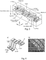
Figure 5 shows a view of a partial section of a thermoelectric generator according to the invention. -
Figure 6 shows in (a) a section of a first substrate of the thermoelectric generator offigure 5 , in (b) a portion of a second substrate of the thermoelectric generator offigure 5 . -
Figure 7 shows a perspective view of a portion of the thermoelectric generator offigure 5 , with a layer of an electrically and thermally isolating material placed on a portion of a first hill of the first substrate, which is shaped as a truncated pyramid, solid or even partially hollow, and coated by a thermoelectric material, the latter being in contact with metal conductors. -
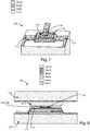
Figure 8 shows a sectional side view of a base element of an embodiment of the thermoelectric generator according to the invention. -
Figure 9 shows a perspective view of elements according tofigure 7 connected in series, according to an aspect of the invention. -
Figure 10 shows a perspective view of elements according tofigure 7 connected in parallel, according to an aspect of the invention. -
Figure 11 shows a perspective view of elements according tofigure 7 connected as a grid, according to an aspect of the invention. -
Figure 12 shows a perspective view of a different base element of an embodiment of the thermoelectric generator according to the invention. -
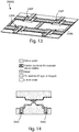
Figure 13 shows a perspective view of elements according tofigure 12 connected as a grid, according to an aspect of the invention. -
Figure 14 shows a further embodiment of the invention, wherein the electrical connections among the building blocks are realized on the back part of the base silicon wafer by means of interconnection VIAS. - Referring to
figures 5-8 , abuilding block 100 of a thermoelectric generator according to the invention is illustrated. - Said part of the
thermoelectric generator 100 comprises: - a first substrate or bottom substrate 110 (silicon wafer);
- a second substrate or top substrate 120 (silicon wafer) facing the bottom substrate.
- In
figure 5 twobase elements 130 are shown, in thebottom substrate 110, withconnections 140, better disclosed in detail hereinafter (seefigures 9, 10 ,11 ). Between the bottom and top substrates there is an air orvacuum gap 150. - Referring to
figure 6(a) , the structure of thebottom substrate 110 is illustrated. It has asurface 111 withhills 111C andvalleys 111V alternated one another. - Referring to
figure 6(b) , the structure of thetop substrate 120 is shown. It has asurface 121 withhills 121C andvalleys 121V alternated one another. - Said
first substrate 110 and saidsecond substrate 120 are facing one another so as eachhill 111C of thefirst substrate 110 is facing to arespective hill 121C of saidsecond substrate 120 and so as eachvalley 111V of thefirst substrate 110 is facing arespective valley 121V of thesecond substrate 120, as it is clear infigure 5 . The respective hills of both layers are in contact through their peak. - The
valleys 111V of the first substrate 1 and thevalleys 121V of the second substrate 2 contribute to increase the thermal resistance of air present in the gap between said substrates. - In the shown embodiment, each of said substrates is composed of a respective silicon wafer.
- Referring to the
bottom substrate 110, on thewhole surface 111 there is afirst layer 114 of electrically isolating material, for example silicon oxide or silicon nitride with a thickness that may range from few nanometers to one micron, in contact with the silicon wafer. - In contact with the first layer of electrically isolating
material 114 there is alocalized layer 115 of electrically isolating material (for example silicon oxide, silicon nitride) that composes the body of thehill 111C. The thickness of thislocalized layer 115 ranges from 1 micron up to hundreds of microns, preferably in the order of tens of microns when the thermoelectric material (illustrated hereinafter) is in the order of hundreds of nanometers. To this hill material a truncated-pyramidal shape with any base shape is imparted, for example a rectangular or square base (in the shown examples), or a truncated-conic shape by means of standard photo-lithographic techniques. The geometry of the material in this zone and its thermal characteristics are such to make a significantly greater thermal resistance than that of the other parts that constitute the base element (the hill material should be electrically isolating and from a thermal point of view it should have a thermal conductivity as low as possible in respect to that of the thermoelectric material). - Below the
localized layer 115 there is a layer ofthermoelectric material 116, of p-type or of n-type. This thermoelectric material is deposited onto all side faces (or onto only two faces only) of the truncated-pyramidal or truncated-conical structure 115 (seefigure 7 ). The thickness may range between 10 and 1000nm, but it could be even greater than 1 micron depending on the particular application for which the TEG is designed. Examples of TE materials are heavily doped semiconductors such as Si or SiGe. - The
first substrate 110 and thesecond substrate 120 may be thinned or ultra-thinned crystalline silicon wafers, for carrying greater flux of heat towards the terminals of the thermoelectric material. - Finally,
metals 117 extending between about one half of a valley and the beginning of a hill, above the first isolatinglayer 114, are deposited. There is still anothermetal 118 at the top of thehill 111C above thethermoelectric material 116. All these metals are electric contacts. The base of themetal 118 that rests on the peak of the hill of the truncated-pyramidal or truncated-conical structure is also a thermal contact. - The
base element 130 of thebottom layer 110 is shown infigure 7 in a perspective view. Ametal 119, that may be considered an extension of themetal 117 and that surrounds the peak of the hill, is shown. - The
electric contacts - Referring to the
top substrate 120, on thewhole surface 121 there is afirst layer 124 of an electrically isolating material, for example silicon oxide or silicon nitride with a thickness that may range between few nanometers and one micron, in contact with the silicon wafer. - An
electric contact 128 is deposited onto the isolatinglayer 124, at the peak of thehill 121C. - The contacts placed at the peak of the hills of the upper layer and of the lower layer are in contact in the device according to the invention.
Figure 8 shows this contact at magnified view. - The silicon wafers mentioned above may be micro-machined, joined together by means of a smart-cut processing or of the technique Smart Stacking™ by Soitec for transferring layers.
- As far as the embodiment of the bottom substrate is concerned (bottom chip,
figure 6(a) ), it is possible to use known technique and future techniques. In particular is it possible to proceed for example as following: - 1) Starting from a monocrystalline silicon substrate, a film of thermal oxide (of a thickness of 1µm or 2µm) is deposited. This oxide will serve as a mask for the following etchings.
- 2) By means of a photolithographic process, openings in the thermal oxide are made for realizing valleys engravings (111V).
- 3) By means of a combination of chemical etchings (Wet) and plasma etchings (Reactive Ion Etch) the valleys (111V) are realized on the silicon substrate of the Bottom Chip.
- 4) A film of thick silicon oxide is deposited (thickness from 1µm to 10µm) through a LPCVD (Low Pressure Chemical Vapour Deposition) technique, a PECVD (Plasma Enhanced Chemical Vapour Deposition) technique or through deposition of SOG (Spin On Glass).
- 5) The hill structures (115) are realized, with a controlled slope [reference OPTICS EXPRESS, Vol. 20, No. 20 / 22934 (2012)], through photolithographic masks and a combination of chemical etchings (Wet) and plasma etchings (Reactive Ion Etch) of the thick silicon oxide.
- 6) A thermal oxide is grown (thickness of several hundreds of nanometers) on the silicon that has been exposed during the previous attacks. This oxide will be used for isolating electrically the substrate.
- 7) The thermoelectric material is deposited ("p" type or "n" type) and, for the photolithography, the active zones of thermoelectric material are delimited on the hills of thick oxide.
- 8) A metal film is deposited by sputtering technique and, by photolithography, the interconnection zones of the Bottom Chip are delimited.
- As far as the realization of the top substrate (
figure 6(b) ) is concerned, it is possible to use known techniques and future techniques. In particular, it is possible to proceed for example as follows: - 1) Starting from a monocrystalline silicon substrate a thermal oxide is grown (of a thickness of 1µm or 2µm). This oxide will serve as a mask for the following etchings.
- 2) By means of a photolithographic process, openings in the thermal oxide are made.
- 3) By means of a combination of chemical etchings (Wet) and plasma etchings (Reactive Ion Etch) the valleys (121V) are realized on the silicon substrate of the Top Chip.
- 4) By Wet etching, the film of thermal oxide is removed.
- 5) A film of silicon nitride is deposited through a LPCVD (Low Pressure Chemical Vapour Deposition) technique or a PECVD (Plasma Enhanced Chemical Vapour Deposition) technique. This film of nitride will serve to isolate electrically the interconnections to be realized on the wafer of the Top Chip, as illustrated in the next step.
- 6) A metal film is deposited through a sputtering technique and by photolithography, the interconnection zones of the Top Chip are delimited.
- This technique refers to the following publications:
- "Semiconductor Devices, Physics and Technology, 2nd edition", S.M. Sze. John Wiley and Sons (2002)
- Handbook of Semiconductor Manufacturing Technology, Second Edition, Yoshio Nishi, Robert Doering. CRC Press (2007)
- "A fully integrated high-Q Whispering-Gallery Wedge Resonator" Fernando Ramiro-Manzano, Nikola Prtljaga, Lorenzo Pavesi, Georg Pucker and Mher Ghulinyan, OPTICS EXPRESS, Vol. 20, No. 20 / 22934 (2012).
- Several features that make the herein proposed device different from those according the prior art are:
- lack of suspended or bridge structures;
- 3D structure of the thermoelectric material with a consequent increase of the capability of transforming heat into electricity;
- greater thermal insulation between the bottom layer and the top layer. Consequently, enhanced capability of thermal coupling with the outside and thus greater capability of thermoelectric conversion;
- better thermal contact among the elements of the bottom substrate and of the top substrate that carry heat (the improvement in respect to the prior art is due to the use of flip-chip bonding or metal-to-metal bonding);
- enhanced management of both thermal and electrical fluxes: the use of a hill material that has a great thermal resistance and the presence of air/vacuum in the cavities, allow to convey better heat inside the TE material. For example in the prior art solution of
figure 3 , the presence of the silicon oxide creates a thermal short circuit between the hot and cold parts; by contrast, in the solution offigure 4 the hot and cold parts are closed than in the herein disclosed solution in which there are engravings in the wafers, as shown atpoints - use of thinned substrates with a consequent reduction of substrate losses. The wafer may be thinned down to the limit of having a structure still mechanically stable (a range could be from 10 to 1000 microns).
- In order to obtain a thermoelectric generator having the maximum temperature difference at the terminals of the thermoelectric material (ΔTeffettivo) an air gap or a gap under vacuum is exploited, in order to allow a better thermal decoupling between the bottom substrate and the top substrate, instead of the oxide layer LOCOS disclosed in the document by Strasser et al.
- By contrast, in respect to the device disclosed in the document by Su, Leonov et al., a greater ΔTeffettivo is obtained because the integration of the bottom substrate and of the top substrate is carried out by means of flip-chip bonding or metal-to-metal bonding, without using adhesives that introduce unavoidably losses of heat flux that determines the ΔTeffettivo. Moreover, the use of thinned substrates allow to reduce the relevant thermal losses. The presence of a bonding through metal or through oxide, instead of bondings that contemplate the use of polymeric materials or thermal pastes, allows also to attain higher temperatures before degradation.
- In order to obtain a TEG starting from a base element, it is necessary to connect in the most appropriate manner more p-type and n-type base elements. The base elements are of n-type when a thermoelectric material constituted by a heavily doped (for example with boron) semiconductor (for example silicon) in which the majority carriers are composed of electrons and of p-type when a thermoelectric material (for example silicon) composed of a heavily doped semiconductor (for example with phosphorous) in which the majority carriers are holes.
- Hereinafter the electrical connection between the two base elements of p-type (100P) and two of n-type (100N) are illustrated:
- a)
Series connection 1000S of two pairs of base elements of p-type and n-type, seefigure 9 . - b)
Parallel connection 1000P of two pairs of base elements p and n, seefigure 10 . - c)
Grid connection 1000G of two pairs of base elements p and n, seefigure 11 . - In
figures 9-11 the different electric connections among base elements are shown, the arrows indicate the sense in which the electric current would flow in the hypothesis in which the top substrate of the thermoelectric generator were in contact with a thermal bath at a temperature Thot and the bottom substrate of the thermoelectric generator were in contact with one at a temperature Tcold. - Another possible embodiment of the proposed invention contemplates a base block of the
bottom layer 230 with a truncated-pyramidal hill 211C, the deposition of thethermoelectric material 216 on two side faces only of the truncated pyramid, and theside 217 and upper 218 electric contacts as shown infigure 12 . - In order to obtain a thermoelectric generator starting from the base element shown in
figure 5 , it is necessary to connect a plurality of base elements of p-type and of n-type as shown hereinbefore. Merely for example,figure 13 depicts thegrid type connection 2000G amongbase elements 230P of p-type and 230N of n-type. - The building blocks are joined by alternating, in the current flux, p-type elements and n-type elements. The union by alignment of the building blocks is carried out according to a chip-on-chip mode, chip-on-wafer, wafer-on-wafer; or according to a chip-on-wafer-on-substrate or chip-on-chip-on-substrate mode.
- Referring to
figure 14 , another advantageous embodiment of the invention is highlighted, in which the electrical connections among said building blocks are realized on the back side of thebase silicon wafer 110 by means of the use of interconnection VIAS. The presence of VIAS constitutes a synergy with the rest of the above disclosed geometry. Indeed, there is a better heat sinking, because heat must follow a path; it shall not go in the substrate but it shall cross it and be sunk beyond the silicon substrate. Moreover in these VIAS electric energy flows therethrough at the same time. The VIAS are preferably realized in a thinned wafer. - Advantageously, the thermal generator, object of the invention, allows to maximize the temperature difference on the terminals of the generator. A second advantage is given by the fact that there are not inside the thermoelectric generator, object of the invention, suspended structures or bridge structures, differently from prior art thermoelectric generators (such as for example those disclosed in the publication by Strasser et al. and in the publication by Su, Leonov et al.). From a mechanical point of view, said suspended structures or bridge structures weaken the structure of the thermoelectric generator and/or make said thermoelectric generator unsuitable to resist to high temperatures (greater than 60°C) and/or to be sealed by means of specific types of bonding, such as for example flip-chip bonding or metal-to-metal bonding.
- As a consequence, the absence of suspended structure or bridge structures makes the thermal generator, object of the invention, more robust from a mechanical point of view. Moreover, the structure can be miniaturized and directly integrated in the traditional electronic devices, or directly onto silicon or in heterogeneous integrations.
- It is possible to organize the base elements in more complex architectures in order to respond to specific application requirements, by placing the base elements electrically in series and/or in parallel in function of the electric amounts that it is desired to obtain at the output. It is possible for example to modify within a certain range the output electrical amounts of the generators by working on the series-parallel electrical interconnections among base elements: for example, if n base elements are all placed electrically in series, the greatest deliverable voltage and the greatest electric resistance (series of n unitary resistances) will be obtained; if the n base elements are placed in parallel, a generator with the minimum resistance (parallel of n unitary resistances) will be obtained; series-parallel connections allow to obtain an electric response that may be modulated between the two ends, either fully in series or fully in parallel.
- The present invention has been disclosed merely for illustrative non limiting purposes, according to a preferred embodiment, but it is understood that variations and/or modifications may be carried out by a skilled person, without for this reason departing from the scope of protection, as defined in the enclosed claims.
Claims (10)
- A building block (100) of an integrated thermoelectric generator with out-of-plane heat flow configuration, comprising a base silicon wafer (110) and a cover silicon wafer (120) each having two opposite faces, wherein:- said base silicon wafer (110) has, on one face of said opposite faces, a plurality of hills (111C) and a plurality of valleys (111V) between said hills (111C);- each of said hills (111C) comprises a first truncated pyramid or cone in the silicon wafer, on which a second truncated pyramid or cone (115) is connected, which is made of electrically and thermally insulating material, wherein the larger base of the second truncated pyramid or cone is smaller than and in contact with the smaller base of the first truncated pyramid or cone in the silicon wafer;- on the smaller base and at least partially on the side surface of said second truncated pyramid or cone is present a layer of p-doped type thermoelectric material (116) which extends also over at least a portion of the smaller base of said first truncated pyramid or cone,- a top electrical contact (118) is present on the smaller base of said second truncated pyramid or cone and two or more side contacts (117) which at one end are in contact with said layer of thermoelectric material on said at least one portion of the smaller base of said first truncated pyramid or cone and extend on the side of said hill (111C) up to a portion of a respective valley (111V);- said cover silicon wafer (120) has on one face of said opposite faces a plurality of valleys (121V) and hills (121C),- on substantially the whole of said one face of the cover silicon wafer (120) there is a layer (124) of electrically insulating material;- on top of the hills (121C) of said cover silicon wafer (120) metallic contacts are placed which serve both as electrical contacts and as top thermal contacts;- said cover silicon wafer is facing said base silicon wafer in such a way that the respective top contacts (118, 128) are in contact and the space between said cover silicon wafer and said base silicon wafer is a space in which vacuum is made or a gas is present, in particular air.
- A building block (100) of an integrated thermoelectric generator according to claim 1, wherein said contacts (117, 118, 128) are made of metal, for example aluminium, copper, silver, or metal alloys.
- A building block (100) of an integrated thermoelectric generator according to claim 1 or 2, wherein on said one face of the base silicon wafer (110) there is a layer (114) of electrically insulating material, with a thickness comprised between 1 nm to 1µm.
- A building block (100) of an integrated thermoelectric generator according to any of claims 1 to 3, wherein said thermoelectric material is a n- or p-type doped semiconductor.
- A building block (100) of an integrated thermoelectric generator according to any of claims 1 to 4, wherein said second truncated pyramid or cone (115) has a height of between 1 micron and 500 microns.
- A building block (100) of the integrated thermoelectric generator according to any of claims 1 to 5, wherein said second truncated pyramid or cone (115) is of a material belonging to the group consisting of: silicon dioxide, oxides with high resistance to heat conduction, lattice structures of nanometric material phonon, and superlattices of silicon nanometric thin film.
- An integrated thermoelectric generator (1000S, 1000P, 1000G) formed by two or more blocks according to any of claims 1 to 6, wherein said two or more blocks are connected to each other by means of said side contacts (117) and said top contacts (128) in such a way that they are connected in series, or in parallel or in a grid, and so that an electric current generated by Seebeck effect flows through alternating blocks with thermoelectric material (116) of n- and p-doped type.
- An integrated thermoelectric generator according to any of claims 1 to 7, wherein between the respective top contacts of the base wafer and the cover a flip-chip bonding is present.
- An integrated thermoelectric generator according to the preceding claim, wherein said base wafer and cover wafer are joined in alignment with a technique belonging to the group comprising or consisting of: metal-to-metal bonding, metal-to-metal thermo-compression, plasma union, union through benzociclobutene, union through polyamides, union through intermetallic compounds, union through solid-liquid interdiffusion (SLID), union by eutectic alloy, copper-oxide union, metal-metal oxide union, anodic union and union through micro-bump.
- An integrated thermoelectric generator according to any of claims 7 to 9, wherein the electrical connections between said constituent blocks are made on the back of the silicon wafer base (110) by the use of vias for interconnection.
Applications Claiming Priority (2)
| Application Number | Priority Date | Filing Date | Title |
|---|---|---|---|
| ITUB2015A005100A ITUB20155100A1 (en) | 2015-10-23 | 2015-10-23 | Thermoelectric generator. |
| PCT/IB2016/056318 WO2017068527A1 (en) | 2015-10-23 | 2016-10-20 | Thermoelectric generator |
Publications (2)
| Publication Number | Publication Date |
|---|---|
| EP3365917A1 EP3365917A1 (en) | 2018-08-29 |
| EP3365917B1 true EP3365917B1 (en) | 2019-12-11 |
Family
ID=55315608
Family Applications (1)
| Application Number | Title | Priority Date | Filing Date |
|---|---|---|---|
| EP16836234.1A Active EP3365917B1 (en) | 2015-10-23 | 2016-10-20 | Thermoelectric generator |
Country Status (6)
| Country | Link |
|---|---|
| US (1) | US10388845B2 (en) |
| EP (1) | EP3365917B1 (en) |
| JP (1) | JP6860561B2 (en) |
| CN (1) | CN108352398B (en) |
| IT (1) | ITUB20155100A1 (en) |
| WO (1) | WO2017068527A1 (en) |
Families Citing this family (2)
| Publication number | Priority date | Publication date | Assignee | Title |
|---|---|---|---|---|
| US12201023B2 (en) | 2021-03-18 | 2025-01-14 | Sumitomo Electric Industries, Ltd. | Thermoelectric-conversion material element and optical sensor containing the same |
| JP7757819B2 (en) | 2022-02-08 | 2025-10-22 | 住友電気工業株式会社 | Optical sensor |
Family Cites Families (18)
| Publication number | Priority date | Publication date | Assignee | Title |
|---|---|---|---|---|
| JPH01138429A (en) * | 1987-07-24 | 1989-05-31 | New Japan Radio Co Ltd | Thermopile |
| JPS6464268A (en) * | 1987-09-03 | 1989-03-10 | New Japan Radio Co Ltd | Thermopile |
| JP2670366B2 (en) * | 1989-11-09 | 1997-10-29 | 日本原子力発電株式会社 | Thermoelectric generator |
| JPH0555639A (en) * | 1991-08-22 | 1993-03-05 | Matsushita Electric Ind Co Ltd | Thermoelectric device |
| JPH10303469A (en) * | 1997-04-23 | 1998-11-13 | Sharp Corp | Thin-film thermoelectric conversion element, semiconductor device using the same, and printed circuit board using the same |
| KR20060024779A (en) * | 2003-05-23 | 2006-03-17 | 코닌클리즈케 필립스 일렉트로닉스 엔.브이. | Thermoelectric device and manufacturing method thereof |
| JP2005259944A (en) * | 2004-03-11 | 2005-09-22 | Nagoya Industrial Science Research Inst | Thin film thermoelectric semiconductor device and manufacturing method thereof |
| KR100668610B1 (en) * | 2004-09-09 | 2007-01-16 | 엘지전자 주식회사 | Thin film thermoelectric module |
| US7544883B2 (en) * | 2004-11-12 | 2009-06-09 | International Business Machines Corporation | Integrated thermoelectric cooling devices and methods for fabricating same |
| KR100690926B1 (en) * | 2006-02-03 | 2007-03-09 | 삼성전자주식회사 | Micro Heat Flux Sensor Array |
| EP1976034A3 (en) | 2007-03-29 | 2011-11-09 | Stichting IMEC Nederland | Method for manufacturing a thermopile, the thermopile thus obtrained and a thermoelectric generator comprising such thermopiles |
| JP2009182226A (en) * | 2008-01-31 | 2009-08-13 | Nec Corp | High frequency amplifier |
| JP2011040663A (en) * | 2009-08-18 | 2011-02-24 | Hioki Ee Corp | Thermopile type infrared detecting element and method of manufacturing the same |
| JP5742174B2 (en) * | 2009-12-09 | 2015-07-01 | ソニー株式会社 | Thermoelectric generator, thermoelectric power generation method, and electric signal detection method |
| JP5589589B2 (en) * | 2010-06-17 | 2014-09-17 | 富士通株式会社 | Thermoelectric element and method for manufacturing thermoelectric element |
| JP2012063222A (en) * | 2010-09-15 | 2012-03-29 | Panasonic Corp | Infrared sensor, and manufacturing method of the same |
| US9620698B2 (en) * | 2013-01-08 | 2017-04-11 | Analog Devices, Inc. | Wafer scale thermoelectric energy harvester |
| US9748466B2 (en) * | 2013-01-08 | 2017-08-29 | Analog Devices, Inc. | Wafer scale thermoelectric energy harvester |
-
2015
- 2015-10-23 IT ITUB2015A005100A patent/ITUB20155100A1/en unknown
-
2016
- 2016-10-20 CN CN201680062102.3A patent/CN108352398B/en not_active Expired - Fee Related
- 2016-10-20 US US15/769,092 patent/US10388845B2/en not_active Expired - Fee Related
- 2016-10-20 JP JP2018520409A patent/JP6860561B2/en not_active Expired - Fee Related
- 2016-10-20 WO PCT/IB2016/056318 patent/WO2017068527A1/en not_active Ceased
- 2016-10-20 EP EP16836234.1A patent/EP3365917B1/en active Active
Non-Patent Citations (1)
| Title |
|---|
| None * |
Also Published As
| Publication number | Publication date |
|---|---|
| WO2017068527A1 (en) | 2017-04-27 |
| EP3365917A1 (en) | 2018-08-29 |
| US10388845B2 (en) | 2019-08-20 |
| CN108352398B (en) | 2022-02-11 |
| JP6860561B2 (en) | 2021-04-14 |
| CN108352398A (en) | 2018-07-31 |
| ITUB20155100A1 (en) | 2017-04-23 |
| JP2018537848A (en) | 2018-12-20 |
| US20180294398A1 (en) | 2018-10-11 |
Similar Documents
| Publication | Publication Date | Title |
|---|---|---|
| EP3198648B1 (en) | Silicon integrated, out-of-plane heat flux thermoelectric generator | |
| US9997691B2 (en) | 3D integrated thermoelectric generator operating in an out-of-plane heat flux configuration with internal voids and heat conduction paths conditioning vias | |
| EP1976034A2 (en) | Method for manufacturing a thermopile, the thermopile thus obtrained and a thermoelectric generator comprising such thermopiles | |
| Yan et al. | MEMS-based thermoelectric–photoelectric integrated power generator | |
| US11641779B2 (en) | Thermoelectric devices and methods for forming thermoelectric devices | |
| CN215496783U (en) | Integrated Thermoelectric Converter | |
| JP7015304B2 (en) | Integrated thermoelectric generators and related manufacturing methods | |
| WO2008094903A2 (en) | Multistage thick film thermoelectric devices | |
| US10388845B2 (en) | Thermoelectric generator | |
| US10003002B2 (en) | Silicon integrated bivalve thermoelectric generator of out-of-plane heat flux configuration | |
| WO2014200884A1 (en) | Thermoelectric module and method of making same | |
| Egbert et al. | Microscale silicon thermoelectric generator with low impedance for energy harvesting | |
| Iulianella et al. | Integrated Thermoelectric Generator and related Method of Fabrication | |
| US20190058103A1 (en) | Thermoelectric micro-module with high leg density for energy harvesting and cooling applications | |
| CN117897032A (en) | Method for manufacturing a thermoelectric structure |
Legal Events
| Date | Code | Title | Description |
|---|---|---|---|
| STAA | Information on the status of an ep patent application or granted ep patent |
Free format text: STATUS: UNKNOWN |
|
| STAA | Information on the status of an ep patent application or granted ep patent |
Free format text: STATUS: THE INTERNATIONAL PUBLICATION HAS BEEN MADE |
|
| PUAI | Public reference made under article 153(3) epc to a published international application that has entered the european phase |
Free format text: ORIGINAL CODE: 0009012 |
|
| STAA | Information on the status of an ep patent application or granted ep patent |
Free format text: STATUS: REQUEST FOR EXAMINATION WAS MADE |
|
| 17P | Request for examination filed |
Effective date: 20180517 |
|
| AK | Designated contracting states |
Kind code of ref document: A1 Designated state(s): AL AT BE BG CH CY CZ DE DK EE ES FI FR GB GR HR HU IE IS IT LI LT LU LV MC MK MT NL NO PL PT RO RS SE SI SK SM TR |
|
| AX | Request for extension of the european patent |
Extension state: BA ME |
|
| RIN1 | Information on inventor provided before grant (corrected) |
Inventor name: GISON, ITALO Inventor name: MASCOLO, DANILO Inventor name: GIUSTI, MARCO Inventor name: LATESSA, GIUSEPPE Inventor name: BUOSCIOLO, ANTONIETTA Inventor name: GAMMARIELLO, GIUSEPPE |
|
| DAV | Request for validation of the european patent (deleted) | ||
| DAX | Request for extension of the european patent (deleted) | ||
| GRAP | Despatch of communication of intention to grant a patent |
Free format text: ORIGINAL CODE: EPIDOSNIGR1 |
|
| STAA | Information on the status of an ep patent application or granted ep patent |
Free format text: STATUS: GRANT OF PATENT IS INTENDED |
|
| INTG | Intention to grant announced |
Effective date: 20190207 |
|
| GRAJ | Information related to disapproval of communication of intention to grant by the applicant or resumption of examination proceedings by the epo deleted |
Free format text: ORIGINAL CODE: EPIDOSDIGR1 |
|
| STAA | Information on the status of an ep patent application or granted ep patent |
Free format text: STATUS: REQUEST FOR EXAMINATION WAS MADE |
|
| INTC | Intention to grant announced (deleted) | ||
| GRAR | Information related to intention to grant a patent recorded |
Free format text: ORIGINAL CODE: EPIDOSNIGR71 |
|
| GRAS | Grant fee paid |
Free format text: ORIGINAL CODE: EPIDOSNIGR3 |
|
| STAA | Information on the status of an ep patent application or granted ep patent |
Free format text: STATUS: GRANT OF PATENT IS INTENDED |
|
| INTG | Intention to grant announced |
Effective date: 20190823 |
|
| GRAA | (expected) grant |
Free format text: ORIGINAL CODE: 0009210 |
|
| STAA | Information on the status of an ep patent application or granted ep patent |
Free format text: STATUS: THE PATENT HAS BEEN GRANTED |
|
| AK | Designated contracting states |
Kind code of ref document: B1 Designated state(s): AL AT BE BG CH CY CZ DE DK EE ES FI FR GB GR HR HU IE IS IT LI LT LU LV MC MK MT NL NO PL PT RO RS SE SI SK SM TR |
|
| REG | Reference to a national code |
Ref country code: GB Ref legal event code: FG4D |
|
| REG | Reference to a national code |
Ref country code: CH Ref legal event code: EP |
|
| REG | Reference to a national code |
Ref country code: AT Ref legal event code: REF Ref document number: 1213055 Country of ref document: AT Kind code of ref document: T Effective date: 20191215 |
|
| REG | Reference to a national code |
Ref country code: DE Ref legal event code: R096 Ref document number: 602016026175 Country of ref document: DE |
|
| REG | Reference to a national code |
Ref country code: IE Ref legal event code: FG4D |
|
| REG | Reference to a national code |
Ref country code: NL Ref legal event code: MP Effective date: 20191211 |
|
| REG | Reference to a national code |
Ref country code: LT Ref legal event code: MG4D |
|
| PG25 | Lapsed in a contracting state [announced via postgrant information from national office to epo] |
Ref country code: FI Free format text: LAPSE BECAUSE OF FAILURE TO SUBMIT A TRANSLATION OF THE DESCRIPTION OR TO PAY THE FEE WITHIN THE PRESCRIBED TIME-LIMIT Effective date: 20191211 Ref country code: NO Free format text: LAPSE BECAUSE OF FAILURE TO SUBMIT A TRANSLATION OF THE DESCRIPTION OR TO PAY THE FEE WITHIN THE PRESCRIBED TIME-LIMIT Effective date: 20200311 Ref country code: SE Free format text: LAPSE BECAUSE OF FAILURE TO SUBMIT A TRANSLATION OF THE DESCRIPTION OR TO PAY THE FEE WITHIN THE PRESCRIBED TIME-LIMIT Effective date: 20191211 Ref country code: LV Free format text: LAPSE BECAUSE OF FAILURE TO SUBMIT A TRANSLATION OF THE DESCRIPTION OR TO PAY THE FEE WITHIN THE PRESCRIBED TIME-LIMIT Effective date: 20191211 Ref country code: LT Free format text: LAPSE BECAUSE OF FAILURE TO SUBMIT A TRANSLATION OF THE DESCRIPTION OR TO PAY THE FEE WITHIN THE PRESCRIBED TIME-LIMIT Effective date: 20191211 Ref country code: GR Free format text: LAPSE BECAUSE OF FAILURE TO SUBMIT A TRANSLATION OF THE DESCRIPTION OR TO PAY THE FEE WITHIN THE PRESCRIBED TIME-LIMIT Effective date: 20200312 Ref country code: BG Free format text: LAPSE BECAUSE OF FAILURE TO SUBMIT A TRANSLATION OF THE DESCRIPTION OR TO PAY THE FEE WITHIN THE PRESCRIBED TIME-LIMIT Effective date: 20200311 |
|
| PG25 | Lapsed in a contracting state [announced via postgrant information from national office to epo] |
Ref country code: HR Free format text: LAPSE BECAUSE OF FAILURE TO SUBMIT A TRANSLATION OF THE DESCRIPTION OR TO PAY THE FEE WITHIN THE PRESCRIBED TIME-LIMIT Effective date: 20191211 Ref country code: RS Free format text: LAPSE BECAUSE OF FAILURE TO SUBMIT A TRANSLATION OF THE DESCRIPTION OR TO PAY THE FEE WITHIN THE PRESCRIBED TIME-LIMIT Effective date: 20191211 |
|
| PG25 | Lapsed in a contracting state [announced via postgrant information from national office to epo] |
Ref country code: AL Free format text: LAPSE BECAUSE OF FAILURE TO SUBMIT A TRANSLATION OF THE DESCRIPTION OR TO PAY THE FEE WITHIN THE PRESCRIBED TIME-LIMIT Effective date: 20191211 |
|
| PG25 | Lapsed in a contracting state [announced via postgrant information from national office to epo] |
Ref country code: PT Free format text: LAPSE BECAUSE OF FAILURE TO SUBMIT A TRANSLATION OF THE DESCRIPTION OR TO PAY THE FEE WITHIN THE PRESCRIBED TIME-LIMIT Effective date: 20200506 Ref country code: NL Free format text: LAPSE BECAUSE OF FAILURE TO SUBMIT A TRANSLATION OF THE DESCRIPTION OR TO PAY THE FEE WITHIN THE PRESCRIBED TIME-LIMIT Effective date: 20191211 Ref country code: RO Free format text: LAPSE BECAUSE OF FAILURE TO SUBMIT A TRANSLATION OF THE DESCRIPTION OR TO PAY THE FEE WITHIN THE PRESCRIBED TIME-LIMIT Effective date: 20191211 Ref country code: EE Free format text: LAPSE BECAUSE OF FAILURE TO SUBMIT A TRANSLATION OF THE DESCRIPTION OR TO PAY THE FEE WITHIN THE PRESCRIBED TIME-LIMIT Effective date: 20191211 Ref country code: ES Free format text: LAPSE BECAUSE OF FAILURE TO SUBMIT A TRANSLATION OF THE DESCRIPTION OR TO PAY THE FEE WITHIN THE PRESCRIBED TIME-LIMIT Effective date: 20191211 Ref country code: CZ Free format text: LAPSE BECAUSE OF FAILURE TO SUBMIT A TRANSLATION OF THE DESCRIPTION OR TO PAY THE FEE WITHIN THE PRESCRIBED TIME-LIMIT Effective date: 20191211 |
|
| PG25 | Lapsed in a contracting state [announced via postgrant information from national office to epo] |
Ref country code: SM Free format text: LAPSE BECAUSE OF FAILURE TO SUBMIT A TRANSLATION OF THE DESCRIPTION OR TO PAY THE FEE WITHIN THE PRESCRIBED TIME-LIMIT Effective date: 20191211 Ref country code: SK Free format text: LAPSE BECAUSE OF FAILURE TO SUBMIT A TRANSLATION OF THE DESCRIPTION OR TO PAY THE FEE WITHIN THE PRESCRIBED TIME-LIMIT Effective date: 20191211 Ref country code: IS Free format text: LAPSE BECAUSE OF FAILURE TO SUBMIT A TRANSLATION OF THE DESCRIPTION OR TO PAY THE FEE WITHIN THE PRESCRIBED TIME-LIMIT Effective date: 20200411 |
|
| REG | Reference to a national code |
Ref country code: DE Ref legal event code: R097 Ref document number: 602016026175 Country of ref document: DE |
|
| REG | Reference to a national code |
Ref country code: AT Ref legal event code: MK05 Ref document number: 1213055 Country of ref document: AT Kind code of ref document: T Effective date: 20191211 |
|
| PLBE | No opposition filed within time limit |
Free format text: ORIGINAL CODE: 0009261 |
|
| STAA | Information on the status of an ep patent application or granted ep patent |
Free format text: STATUS: NO OPPOSITION FILED WITHIN TIME LIMIT |
|
| PG25 | Lapsed in a contracting state [announced via postgrant information from national office to epo] |
Ref country code: DK Free format text: LAPSE BECAUSE OF FAILURE TO SUBMIT A TRANSLATION OF THE DESCRIPTION OR TO PAY THE FEE WITHIN THE PRESCRIBED TIME-LIMIT Effective date: 20191211 |
|
| 26N | No opposition filed |
Effective date: 20200914 |
|
| PG25 | Lapsed in a contracting state [announced via postgrant information from national office to epo] |
Ref country code: AT Free format text: LAPSE BECAUSE OF FAILURE TO SUBMIT A TRANSLATION OF THE DESCRIPTION OR TO PAY THE FEE WITHIN THE PRESCRIBED TIME-LIMIT Effective date: 20191211 Ref country code: SI Free format text: LAPSE BECAUSE OF FAILURE TO SUBMIT A TRANSLATION OF THE DESCRIPTION OR TO PAY THE FEE WITHIN THE PRESCRIBED TIME-LIMIT Effective date: 20191211 |
|
| PG25 | Lapsed in a contracting state [announced via postgrant information from national office to epo] |
Ref country code: PL Free format text: LAPSE BECAUSE OF FAILURE TO SUBMIT A TRANSLATION OF THE DESCRIPTION OR TO PAY THE FEE WITHIN THE PRESCRIBED TIME-LIMIT Effective date: 20191211 |
|
| REG | Reference to a national code |
Ref country code: CH Ref legal event code: PL |
|
| PG25 | Lapsed in a contracting state [announced via postgrant information from national office to epo] |
Ref country code: MC Free format text: LAPSE BECAUSE OF FAILURE TO SUBMIT A TRANSLATION OF THE DESCRIPTION OR TO PAY THE FEE WITHIN THE PRESCRIBED TIME-LIMIT Effective date: 20191211 Ref country code: LU Free format text: LAPSE BECAUSE OF NON-PAYMENT OF DUE FEES Effective date: 20201020 |
|
| REG | Reference to a national code |
Ref country code: BE Ref legal event code: MM Effective date: 20201031 |
|
| PG25 | Lapsed in a contracting state [announced via postgrant information from national office to epo] |
Ref country code: LI Free format text: LAPSE BECAUSE OF NON-PAYMENT OF DUE FEES Effective date: 20201031 Ref country code: CH Free format text: LAPSE BECAUSE OF NON-PAYMENT OF DUE FEES Effective date: 20201031 Ref country code: BE Free format text: LAPSE BECAUSE OF NON-PAYMENT OF DUE FEES Effective date: 20201031 |
|
| PG25 | Lapsed in a contracting state [announced via postgrant information from national office to epo] |
Ref country code: IE Free format text: LAPSE BECAUSE OF NON-PAYMENT OF DUE FEES Effective date: 20201020 |
|
| PGFP | Annual fee paid to national office [announced via postgrant information from national office to epo] |
Ref country code: DE Payment date: 20211020 Year of fee payment: 6 Ref country code: GB Payment date: 20211022 Year of fee payment: 6 |
|
| PGFP | Annual fee paid to national office [announced via postgrant information from national office to epo] |
Ref country code: IT Payment date: 20211001 Year of fee payment: 6 Ref country code: FR Payment date: 20211022 Year of fee payment: 6 |
|
| PG25 | Lapsed in a contracting state [announced via postgrant information from national office to epo] |
Ref country code: TR Free format text: LAPSE BECAUSE OF FAILURE TO SUBMIT A TRANSLATION OF THE DESCRIPTION OR TO PAY THE FEE WITHIN THE PRESCRIBED TIME-LIMIT Effective date: 20191211 Ref country code: MT Free format text: LAPSE BECAUSE OF FAILURE TO SUBMIT A TRANSLATION OF THE DESCRIPTION OR TO PAY THE FEE WITHIN THE PRESCRIBED TIME-LIMIT Effective date: 20191211 Ref country code: CY Free format text: LAPSE BECAUSE OF FAILURE TO SUBMIT A TRANSLATION OF THE DESCRIPTION OR TO PAY THE FEE WITHIN THE PRESCRIBED TIME-LIMIT Effective date: 20191211 |
|
| PG25 | Lapsed in a contracting state [announced via postgrant information from national office to epo] |
Ref country code: MK Free format text: LAPSE BECAUSE OF FAILURE TO SUBMIT A TRANSLATION OF THE DESCRIPTION OR TO PAY THE FEE WITHIN THE PRESCRIBED TIME-LIMIT Effective date: 20191211 |
|
| REG | Reference to a national code |
Ref country code: DE Ref legal event code: R079 Ref document number: 602016026175 Country of ref document: DE Free format text: PREVIOUS MAIN CLASS: H01L0027160000 Ipc: H10N0019000000 |
|
| REG | Reference to a national code |
Ref country code: DE Ref legal event code: R119 Ref document number: 602016026175 Country of ref document: DE |
|
| GBPC | Gb: european patent ceased through non-payment of renewal fee |
Effective date: 20221020 |
|
| PG25 | Lapsed in a contracting state [announced via postgrant information from national office to epo] |
Ref country code: FR Free format text: LAPSE BECAUSE OF NON-PAYMENT OF DUE FEES Effective date: 20221031 Ref country code: DE Free format text: LAPSE BECAUSE OF NON-PAYMENT OF DUE FEES Effective date: 20230503 |
|
| PG25 | Lapsed in a contracting state [announced via postgrant information from national office to epo] |
Ref country code: IT Free format text: LAPSE BECAUSE OF NON-PAYMENT OF DUE FEES Effective date: 20221020 Ref country code: GB Free format text: LAPSE BECAUSE OF NON-PAYMENT OF DUE FEES Effective date: 20221020 |