EP3361841A1 - Method for manufacturing multilayer ceramic substrate - Google Patents
Method for manufacturing multilayer ceramic substrate Download PDFInfo
- Publication number
- EP3361841A1 EP3361841A1 EP16853478.2A EP16853478A EP3361841A1 EP 3361841 A1 EP3361841 A1 EP 3361841A1 EP 16853478 A EP16853478 A EP 16853478A EP 3361841 A1 EP3361841 A1 EP 3361841A1
- Authority
- EP
- European Patent Office
- Prior art keywords
- green sheet
- thermal expansion
- layer
- cavity
- ceramic substrate
- Prior art date
- Legal status (The legal status is an assumption and is not a legal conclusion. Google has not performed a legal analysis and makes no representation as to the accuracy of the status listed.)
- Granted
Links
Images







Classifications
-
- H—ELECTRICITY
- H05—ELECTRIC TECHNIQUES NOT OTHERWISE PROVIDED FOR
- H05K—PRINTED CIRCUITS; CASINGS OR CONSTRUCTIONAL DETAILS OF ELECTRIC APPARATUS; MANUFACTURE OF ASSEMBLAGES OF ELECTRICAL COMPONENTS
- H05K3/00—Apparatus or processes for manufacturing printed circuits
- H05K3/46—Manufacturing multilayer circuits
- H05K3/4611—Manufacturing multilayer circuits by laminating two or more circuit boards
- H05K3/4626—Manufacturing multilayer circuits by laminating two or more circuit boards characterised by the insulating layers or materials
- H05K3/4629—Manufacturing multilayer circuits by laminating two or more circuit boards characterised by the insulating layers or materials laminating inorganic sheets comprising printed circuits, e.g. green ceramic sheets
-
- B—PERFORMING OPERATIONS; TRANSPORTING
- B32—LAYERED PRODUCTS
- B32B—LAYERED PRODUCTS, i.e. PRODUCTS BUILT-UP OF STRATA OF FLAT OR NON-FLAT, e.g. CELLULAR OR HONEYCOMB, FORM
- B32B18/00—Layered products essentially comprising ceramics, e.g. refractory products
-
- B—PERFORMING OPERATIONS; TRANSPORTING
- B32—LAYERED PRODUCTS
- B32B—LAYERED PRODUCTS, i.e. PRODUCTS BUILT-UP OF STRATA OF FLAT OR NON-FLAT, e.g. CELLULAR OR HONEYCOMB, FORM
- B32B37/00—Methods or apparatus for laminating, e.g. by curing or by ultrasonic bonding
- B32B37/06—Methods or apparatus for laminating, e.g. by curing or by ultrasonic bonding characterised by the heating method
-
- B—PERFORMING OPERATIONS; TRANSPORTING
- B32—LAYERED PRODUCTS
- B32B—LAYERED PRODUCTS, i.e. PRODUCTS BUILT-UP OF STRATA OF FLAT OR NON-FLAT, e.g. CELLULAR OR HONEYCOMB, FORM
- B32B37/00—Methods or apparatus for laminating, e.g. by curing or by ultrasonic bonding
- B32B37/10—Methods or apparatus for laminating, e.g. by curing or by ultrasonic bonding characterised by the pressing technique, e.g. using action of vacuum or fluid pressure
-
- B—PERFORMING OPERATIONS; TRANSPORTING
- B32—LAYERED PRODUCTS
- B32B—LAYERED PRODUCTS, i.e. PRODUCTS BUILT-UP OF STRATA OF FLAT OR NON-FLAT, e.g. CELLULAR OR HONEYCOMB, FORM
- B32B38/00—Ancillary operations in connection with laminating processes
- B32B38/10—Removing layers, or parts of layers, mechanically or chemically
-
- H—ELECTRICITY
- H05—ELECTRIC TECHNIQUES NOT OTHERWISE PROVIDED FOR
- H05K—PRINTED CIRCUITS; CASINGS OR CONSTRUCTIONAL DETAILS OF ELECTRIC APPARATUS; MANUFACTURE OF ASSEMBLAGES OF ELECTRICAL COMPONENTS
- H05K3/00—Apparatus or processes for manufacturing printed circuits
- H05K3/46—Manufacturing multilayer circuits
-
- H—ELECTRICITY
- H05—ELECTRIC TECHNIQUES NOT OTHERWISE PROVIDED FOR
- H05K—PRINTED CIRCUITS; CASINGS OR CONSTRUCTIONAL DETAILS OF ELECTRIC APPARATUS; MANUFACTURE OF ASSEMBLAGES OF ELECTRICAL COMPONENTS
- H05K3/00—Apparatus or processes for manufacturing printed circuits
- H05K3/46—Manufacturing multilayer circuits
- H05K3/4697—Manufacturing multilayer circuits having cavities, e.g. for mounting components
-
- H—ELECTRICITY
- H10—SEMICONDUCTOR DEVICES; ELECTRIC SOLID-STATE DEVICES NOT OTHERWISE PROVIDED FOR
- H10W—GENERIC PACKAGES, INTERCONNECTIONS, CONNECTORS OR OTHER CONSTRUCTIONAL DETAILS OF DEVICES COVERED BY CLASS H10
- H10W70/00—Package substrates; Interposers; Redistribution layers [RDL]
- H10W70/01—Manufacture or treatment
- H10W70/05—Manufacture or treatment of insulating or insulated package substrates, or of interposers, or of redistribution layers
-
- H—ELECTRICITY
- H10—SEMICONDUCTOR DEVICES; ELECTRIC SOLID-STATE DEVICES NOT OTHERWISE PROVIDED FOR
- H10W—GENERIC PACKAGES, INTERCONNECTIONS, CONNECTORS OR OTHER CONSTRUCTIONAL DETAILS OF DEVICES COVERED BY CLASS H10
- H10W70/00—Package substrates; Interposers; Redistribution layers [RDL]
- H10W70/01—Manufacture or treatment
- H10W70/05—Manufacture or treatment of insulating or insulated package substrates, or of interposers, or of redistribution layers
- H10W70/095—Manufacture or treatment of insulating or insulated package substrates, or of interposers, or of redistribution layers of vias therein
-
- H—ELECTRICITY
- H10—SEMICONDUCTOR DEVICES; ELECTRIC SOLID-STATE DEVICES NOT OTHERWISE PROVIDED FOR
- H10W—GENERIC PACKAGES, INTERCONNECTIONS, CONNECTORS OR OTHER CONSTRUCTIONAL DETAILS OF DEVICES COVERED BY CLASS H10
- H10W70/00—Package substrates; Interposers; Redistribution layers [RDL]
- H10W70/60—Insulating or insulated package substrates; Interposers; Redistribution layers
-
- H—ELECTRICITY
- H10—SEMICONDUCTOR DEVICES; ELECTRIC SOLID-STATE DEVICES NOT OTHERWISE PROVIDED FOR
- H10W—GENERIC PACKAGES, INTERCONNECTIONS, CONNECTORS OR OTHER CONSTRUCTIONAL DETAILS OF DEVICES COVERED BY CLASS H10
- H10W70/00—Package substrates; Interposers; Redistribution layers [RDL]
- H10W70/60—Insulating or insulated package substrates; Interposers; Redistribution layers
- H10W70/62—Insulating or insulated package substrates; Interposers; Redistribution layers characterised by their interconnections
- H10W70/63—Vias, e.g. via plugs
- H10W70/635—Through-vias
-
- H—ELECTRICITY
- H10—SEMICONDUCTOR DEVICES; ELECTRIC SOLID-STATE DEVICES NOT OTHERWISE PROVIDED FOR
- H10W—GENERIC PACKAGES, INTERCONNECTIONS, CONNECTORS OR OTHER CONSTRUCTIONAL DETAILS OF DEVICES COVERED BY CLASS H10
- H10W70/00—Package substrates; Interposers; Redistribution layers [RDL]
- H10W70/60—Insulating or insulated package substrates; Interposers; Redistribution layers
- H10W70/62—Insulating or insulated package substrates; Interposers; Redistribution layers characterised by their interconnections
- H10W70/65—Shapes or dispositions of interconnections
-
- H—ELECTRICITY
- H10—SEMICONDUCTOR DEVICES; ELECTRIC SOLID-STATE DEVICES NOT OTHERWISE PROVIDED FOR
- H10W—GENERIC PACKAGES, INTERCONNECTIONS, CONNECTORS OR OTHER CONSTRUCTIONAL DETAILS OF DEVICES COVERED BY CLASS H10
- H10W70/00—Package substrates; Interposers; Redistribution layers [RDL]
- H10W70/60—Insulating or insulated package substrates; Interposers; Redistribution layers
- H10W70/67—Insulating or insulated package substrates; Interposers; Redistribution layers characterised by their insulating layers or insulating parts
- H10W70/68—Shapes or dispositions thereof
-
- H—ELECTRICITY
- H10—SEMICONDUCTOR DEVICES; ELECTRIC SOLID-STATE DEVICES NOT OTHERWISE PROVIDED FOR
- H10W—GENERIC PACKAGES, INTERCONNECTIONS, CONNECTORS OR OTHER CONSTRUCTIONAL DETAILS OF DEVICES COVERED BY CLASS H10
- H10W70/00—Package substrates; Interposers; Redistribution layers [RDL]
- H10W70/60—Insulating or insulated package substrates; Interposers; Redistribution layers
- H10W70/67—Insulating or insulated package substrates; Interposers; Redistribution layers characterised by their insulating layers or insulating parts
- H10W70/68—Shapes or dispositions thereof
- H10W70/685—Shapes or dispositions thereof comprising multiple insulating layers
-
- B—PERFORMING OPERATIONS; TRANSPORTING
- B32—LAYERED PRODUCTS
- B32B—LAYERED PRODUCTS, i.e. PRODUCTS BUILT-UP OF STRATA OF FLAT OR NON-FLAT, e.g. CELLULAR OR HONEYCOMB, FORM
- B32B2315/00—Other materials containing non-metallic inorganic compounds not provided for in groups B32B2311/00 - B32B2313/04
- B32B2315/02—Ceramics
-
- B—PERFORMING OPERATIONS; TRANSPORTING
- B32—LAYERED PRODUCTS
- B32B—LAYERED PRODUCTS, i.e. PRODUCTS BUILT-UP OF STRATA OF FLAT OR NON-FLAT, e.g. CELLULAR OR HONEYCOMB, FORM
- B32B2457/00—Electrical equipment
-
- H—ELECTRICITY
- H05—ELECTRIC TECHNIQUES NOT OTHERWISE PROVIDED FOR
- H05K—PRINTED CIRCUITS; CASINGS OR CONSTRUCTIONAL DETAILS OF ELECTRIC APPARATUS; MANUFACTURE OF ASSEMBLAGES OF ELECTRICAL COMPONENTS
- H05K1/00—Printed circuits
- H05K1/18—Printed circuits structurally associated with non-printed electric components
- H05K1/182—Printed circuits structurally associated with non-printed electric components associated with components mounted in printed circuit boards [PCB], e.g. insert-mounted components [IMC]
- H05K1/183—Printed circuits structurally associated with non-printed electric components associated with components mounted in printed circuit boards [PCB], e.g. insert-mounted components [IMC] associated with components mounted in and supported by recessed areas of the PCBs
-
- H—ELECTRICITY
- H10—SEMICONDUCTOR DEVICES; ELECTRIC SOLID-STATE DEVICES NOT OTHERWISE PROVIDED FOR
- H10W—GENERIC PACKAGES, INTERCONNECTIONS, CONNECTORS OR OTHER CONSTRUCTIONAL DETAILS OF DEVICES COVERED BY CLASS H10
- H10W70/00—Package substrates; Interposers; Redistribution layers [RDL]
- H10W70/60—Insulating or insulated package substrates; Interposers; Redistribution layers
- H10W70/67—Insulating or insulated package substrates; Interposers; Redistribution layers characterised by their insulating layers or insulating parts
- H10W70/68—Shapes or dispositions thereof
- H10W70/682—Shapes or dispositions thereof comprising holes having chips therein
-
- H—ELECTRICITY
- H10—SEMICONDUCTOR DEVICES; ELECTRIC SOLID-STATE DEVICES NOT OTHERWISE PROVIDED FOR
- H10W—GENERIC PACKAGES, INTERCONNECTIONS, CONNECTORS OR OTHER CONSTRUCTIONAL DETAILS OF DEVICES COVERED BY CLASS H10
- H10W70/00—Package substrates; Interposers; Redistribution layers [RDL]
- H10W70/60—Insulating or insulated package substrates; Interposers; Redistribution layers
- H10W70/67—Insulating or insulated package substrates; Interposers; Redistribution layers characterised by their insulating layers or insulating parts
- H10W70/69—Insulating materials thereof
- H10W70/692—Ceramics or glasses
-
- H—ELECTRICITY
- H10—SEMICONDUCTOR DEVICES; ELECTRIC SOLID-STATE DEVICES NOT OTHERWISE PROVIDED FOR
- H10W—GENERIC PACKAGES, INTERCONNECTIONS, CONNECTORS OR OTHER CONSTRUCTIONAL DETAILS OF DEVICES COVERED BY CLASS H10
- H10W72/00—Interconnections or connectors in packages
- H10W72/071—Connecting or disconnecting
- H10W72/072—Connecting or disconnecting of bump connectors
- H10W72/07231—Techniques
- H10W72/07236—Soldering or alloying
-
- H—ELECTRICITY
- H10—SEMICONDUCTOR DEVICES; ELECTRIC SOLID-STATE DEVICES NOT OTHERWISE PROVIDED FOR
- H10W—GENERIC PACKAGES, INTERCONNECTIONS, CONNECTORS OR OTHER CONSTRUCTIONAL DETAILS OF DEVICES COVERED BY CLASS H10
- H10W72/00—Interconnections or connectors in packages
- H10W72/20—Bump connectors, e.g. solder bumps or copper pillars; Dummy bumps; Thermal bumps
- H10W72/29—Bond pads specially adapted therefor
-
- H—ELECTRICITY
- H10—SEMICONDUCTOR DEVICES; ELECTRIC SOLID-STATE DEVICES NOT OTHERWISE PROVIDED FOR
- H10W—GENERIC PACKAGES, INTERCONNECTIONS, CONNECTORS OR OTHER CONSTRUCTIONAL DETAILS OF DEVICES COVERED BY CLASS H10
- H10W72/00—Interconnections or connectors in packages
- H10W72/30—Die-attach connectors
- H10W72/351—Materials of die-attach connectors
- H10W72/352—Materials of die-attach connectors comprising metals or metalloids, e.g. solders
-
- H—ELECTRICITY
- H10—SEMICONDUCTOR DEVICES; ELECTRIC SOLID-STATE DEVICES NOT OTHERWISE PROVIDED FOR
- H10W—GENERIC PACKAGES, INTERCONNECTIONS, CONNECTORS OR OTHER CONSTRUCTIONAL DETAILS OF DEVICES COVERED BY CLASS H10
- H10W72/00—Interconnections or connectors in packages
- H10W72/30—Die-attach connectors
- H10W72/351—Materials of die-attach connectors
- H10W72/353—Materials of die-attach connectors not comprising solid metals or solid metalloids, e.g. ceramics
- H10W72/354—Materials of die-attach connectors not comprising solid metals or solid metalloids, e.g. ceramics comprising polymers
-
- H—ELECTRICITY
- H10—SEMICONDUCTOR DEVICES; ELECTRIC SOLID-STATE DEVICES NOT OTHERWISE PROVIDED FOR
- H10W—GENERIC PACKAGES, INTERCONNECTIONS, CONNECTORS OR OTHER CONSTRUCTIONAL DETAILS OF DEVICES COVERED BY CLASS H10
- H10W72/00—Interconnections or connectors in packages
- H10W72/50—Bond wires
- H10W72/541—Dispositions of bond wires
- H10W72/5445—Dispositions of bond wires being orthogonal to a side surface of the chip, e.g. parallel arrangements
-
- H—ELECTRICITY
- H10—SEMICONDUCTOR DEVICES; ELECTRIC SOLID-STATE DEVICES NOT OTHERWISE PROVIDED FOR
- H10W—GENERIC PACKAGES, INTERCONNECTIONS, CONNECTORS OR OTHER CONSTRUCTIONAL DETAILS OF DEVICES COVERED BY CLASS H10
- H10W72/00—Interconnections or connectors in packages
- H10W72/50—Bond wires
- H10W72/59—Bond pads specially adapted therefor
-
- H—ELECTRICITY
- H10—SEMICONDUCTOR DEVICES; ELECTRIC SOLID-STATE DEVICES NOT OTHERWISE PROVIDED FOR
- H10W—GENERIC PACKAGES, INTERCONNECTIONS, CONNECTORS OR OTHER CONSTRUCTIONAL DETAILS OF DEVICES COVERED BY CLASS H10
- H10W72/00—Interconnections or connectors in packages
- H10W72/851—Dispositions of multiple connectors or interconnections
- H10W72/874—On different surfaces
- H10W72/884—Die-attach connectors and bond wires
-
- H—ELECTRICITY
- H10—SEMICONDUCTOR DEVICES; ELECTRIC SOLID-STATE DEVICES NOT OTHERWISE PROVIDED FOR
- H10W—GENERIC PACKAGES, INTERCONNECTIONS, CONNECTORS OR OTHER CONSTRUCTIONAL DETAILS OF DEVICES COVERED BY CLASS H10
- H10W90/00—Package configurations
-
- H—ELECTRICITY
- H10—SEMICONDUCTOR DEVICES; ELECTRIC SOLID-STATE DEVICES NOT OTHERWISE PROVIDED FOR
- H10W—GENERIC PACKAGES, INTERCONNECTIONS, CONNECTORS OR OTHER CONSTRUCTIONAL DETAILS OF DEVICES COVERED BY CLASS H10
- H10W90/00—Package configurations
- H10W90/701—Package configurations characterised by the relative positions of pads or connectors relative to package parts
- H10W90/721—Package configurations characterised by the relative positions of pads or connectors relative to package parts of bump connectors
- H10W90/724—Package configurations characterised by the relative positions of pads or connectors relative to package parts of bump connectors between a chip and a stacked insulating package substrate, interposer or RDL
-
- H—ELECTRICITY
- H10—SEMICONDUCTOR DEVICES; ELECTRIC SOLID-STATE DEVICES NOT OTHERWISE PROVIDED FOR
- H10W—GENERIC PACKAGES, INTERCONNECTIONS, CONNECTORS OR OTHER CONSTRUCTIONAL DETAILS OF DEVICES COVERED BY CLASS H10
- H10W90/00—Package configurations
- H10W90/701—Package configurations characterised by the relative positions of pads or connectors relative to package parts
- H10W90/731—Package configurations characterised by the relative positions of pads or connectors relative to package parts of die-attach connectors
- H10W90/734—Package configurations characterised by the relative positions of pads or connectors relative to package parts of die-attach connectors between a chip and a stacked insulating package substrate, interposer or RDL
-
- H—ELECTRICITY
- H10—SEMICONDUCTOR DEVICES; ELECTRIC SOLID-STATE DEVICES NOT OTHERWISE PROVIDED FOR
- H10W—GENERIC PACKAGES, INTERCONNECTIONS, CONNECTORS OR OTHER CONSTRUCTIONAL DETAILS OF DEVICES COVERED BY CLASS H10
- H10W90/00—Package configurations
- H10W90/701—Package configurations characterised by the relative positions of pads or connectors relative to package parts
- H10W90/751—Package configurations characterised by the relative positions of pads or connectors relative to package parts of bond wires
- H10W90/754—Package configurations characterised by the relative positions of pads or connectors relative to package parts of bond wires between a chip and a stacked insulating package substrate, interposer or RDL
Definitions
- the present invention relates to a method of prducing a multi-layer ceramic substrate having a cavity.
- Multi-layer ceramic substrates have been widely used as wiring substrates for use in various electronic devices such as communication devices.
- Using a multi-layer ceramic substrate it is possible to incorporate passive elements, such as capacitors, coils and transmission paths, into the substrate and implement electronic components on the surface of the substrate, thus realizing a small module.
- passive elements such as capacitors, coils and transmission paths
- a cavity is provided in a multi-layer ceramic substrate and a semiconductor IC is accommodated in the cavity so as to achieve a low profile of the module as a whole and to highly integrate and combine functions together.
- Such a multi-layer ceramic substrate with a cavity is commonly produced by laminating and pressure-bonding together a ceramic green sheet having an opening corresponding to the cavity and a ceramic green sheet having no opening, and then sintering the ceramic green sheets.
- a ceramic green sheet having an opening is likely to deform when pressure-bonded.
- Patent Document No. 1 discloses a method of prducing a multi-layer ceramic substrate with a cavity, wherein a ceramic green sheet laminate is produced by providing a peel-off layer sandwiched at a position to be the bottom of the cavity, making a slit that reaches the peel-off layer from one primary surface of the laminate before or after the preliminary sintering (debindering process), removing a portion of the green sheet that corresponds to the cavity, and then sintering the laminate.
- Patent Document No. 2 discloses a method of prducing a multi-layer ceramic substrate with a cavity, wherein a ceramic green sheet laminate is produced by providing a burn-out material layer sandwiched at a position to be the bottom of the cavity, and grooving the laminate from one primary surface thereof before or after co-firing the laminate, so that the burn-out material layer is burnt out in the co-firing process, thus producing an internal space, whereby the cavity portion can be removed.
- a method of prducing a multi-layer ceramic substrate of the present invention includes the steps of: (A) preparing a first ceramic green sheet with a thermal expansion layer arranged thereon, and at least one second ceramic green sheet with no thermal expansion layer arranged thereon; (B) laminating the first and second ceramic green sheets with the thermal expansion layer sandwiched therebetween, thereby obtaining a green sheet laminate; (C) pressure-bonding together the first ceramic green sheet and the at least one second ceramic green sheet of the green sheet laminate; (D) heating and thereby expanding the thermal expansion layer at least in a thickness direction in the pressure-bonded green sheet laminate; (E) extracting a portion of the green sheet laminate that has been displaced by the expansion of the thermal expansion layer, thereby forming a cavity in the green sheet laminate; and (F) sintering the green sheet laminate with the cavity formed therein.
- the thermal expansion layer may be held at a temperature higher than a temperature for pressure-bonding in the step (C).
- the thermal expansion layer may include a thermal expansion material whose thickness increases by a factor of 2 or more by being heated.
- the thermal expansion layer may be a layer of a paste including thermally-expansive microcapsules made of a thermoplastic resin that encapsulate a hydrocarbon that is in liquid form at normal temperature.
- the method may further include, between the step (C) and the step (D), a step of forming, in the green sheet laminate, a groove that has a depth of the cavity of the green sheet laminate and defines an outline of the cavity.
- the thermal expansion layer may be removed in the step (E).
- a third ceramic green sheet with another thermal expansion layer arranged thereon may be prepared in a region different from the first ceramic green sheet; in the step (B), the first to third ceramic green sheets may be laminated together so that the thermal expansion layers are sandwiched therebetween, thereby obtaining the green sheet laminate; in the step (D), the other thermal expansion layer may be heated to be expanded at least in the thickness direction; and in the step (E), a portion of the green sheet laminate that has been displaced by the expansion of the other thermal expansion layer may be extracted.
- the method may further include, between the step (E) and the step (F), a step (G) of removing a binder from the green sheet laminate.
- the thermal expansion layer may be held at a temperature that is higher than a temperature for pressure-bonding in the step (C) and lower than a temperature for binder removing in the step (G).
- At least one of the first ceramic green sheet and the second ceramic green sheet may include a pattern to be internal wiring, an inductor, a condenser, a stripline or an internal resistor.
- the first ceramic green sheet may further include a conductor pattern located between the thermal expansion layer and the first ceramic green sheet.
- At least one of the first ceramic green sheet and the second ceramic green sheet may further include a via hole and a conductive paste that fills the via hole.
- a method of prducing a multi-layer ceramic substrate which has a good mass productivity and with which it is easy to extract a portion corresponding to the cavity.
- Patent Document Nos. 1 and 2 The present inventor made an in-depth study on the methods for manufacturing a multi-layer ceramic substrate disclosed in Patent Document Nos. 1 and 2. According to the methods of Patent Document Nos. 1 and 2, there is a need to form a slit or a groove reaching a peel-off layer or a burn-out layer in order to extract a portion of a green sheet corresponding to the cavity or a portion of a sinter corresponding to the cavity. It is difficult to separate the portion corresponding to the cavity unless the slit or groove is aligned with the position of the peel-off layer or burn-out layer and reliably extends to reach the peel-off layer or burn-out layer. Particularly, with the method of Patent Document No. 2, whether the portion corresponding to the cavity can be separated is known after the co-firing process, and it is therefore necessary to perform the manufacturing process up to the co-firing process even if it is a defective product.
- the peel-off layer is made of a material such that the ceramic green sheet can be peeled off easily, a green sheet laminate with the peel-off layer interposed therein will have an insufficient adhesion between the peel-off layer and the ceramic green sheet. Therefore, the pressure-bonded green sheet laminate may have an insufficient form stability or a green sheet may be shifted when forming a slit.
- a green sheet laminate as used in the description below is what is obtained by laminating first and second ceramic green sheets together, and every state from lamination until sintering is defined as a green sheet laminate, irrespective of the order and number of the sheets, the positions and number of thermal expansion layers, and the presence/absence of internal wiring or elements arranged inside the laminate.
- FIG. 1(a) is a perspective view showing an example of a multi-layer ceramic substrate of the present embodiment
- FIG. 1(b) shows a cross section taken along line 1B-1B of FIG. 1(a) .
- a multi-layer ceramic substrate 101 includes a ceramic sinter 110 having an upper surface 110a and a lower surface 110b.
- the upper surface 110a is provided with a cavity 111 for accommodating an electronic component such as a semiconductor IC chip.
- the cavity 111 has a recessed shape having an opening on the upper surface 110a.
- One electrode 112 or a plurality of electrodes 112 may be provided on the upper surface 110a.
- One electrode 113 or a plurality of electrodes 113 may be provided on the lower surface 110b.
- a heat-radiating electrode 114 is provided on a bottom portion 111a of the cavity 111 in order to radiate heat from the semiconductor IC accommodated in the cavity 111.
- the multi-layer ceramic substrate 101 shown in FIG. 1 includes one cavity 111, the multi-layer ceramic substrate may include two or more cavities. In this case, bottom portions 111a may be at the same level or at different levels in two or more cavities 111, as will be described below.
- a passive element pattern 118 and a conductive via 120 and a wiring pattern 119 may be provided inside the ceramic sinter 110.
- the passive element pattern 118 may have a conductivity or a predetermined resistance value, for example, and may form internal wiring, an inductor, a condenser, a stripline, an internal resistor, or the like.
- the wiring pattern 119 is made of a conductive thin-layer pattern that is generally parallel to the upper surface 110a and the lower surface 110b.
- the conductive via 120 is made of a via hole extending in a direction connecting between the upper surface 110a and the lower surface 110b, and a columnar-shaped conductor filling the via hole.
- the wiring pattern 119 and the conductive via 120 are connected to the passive element pattern 118, the wiring pattern 119, the electrode 112, the electrode 113, the electrode 114, etc., thereby forming a predetermined circuit.
- the conductive via 120 connected to the heat-radiating electrode 114 may reach the lower surface 110b as a radiator.
- a heat-radiating electrode 115 that is connected to the conductive via 120 connected to the heat-radiating electrode 114 may be further provided on the lower surface 110b.
- the multi-layer ceramic substrate 101 may be a low temperature co-fired ceramic (LTCC) substrate or a high temperature co-fired ceramic (HTCC) substrate.
- LTCC low temperature co-fired ceramic
- HTCC high temperature co-fired ceramic
- a ceramic material and a conductive material that can be sintered in a temperature range of about 800°C to about 1000°C are used.
- the ceramic material used may be a ceramic material including Al, Si and Sr as its main components and Ti, Bi, Cu, Mn, Na and K as its sub-components, a ceramic material including Al, Si and Sr as its main components and Ca, Pb, Na and K as its sub-components, a ceramic material including Al, Mg, Si and Gd, and a ceramic material including Al, Si, Zr and Mg.
- the conductive material used may be a conductive material including Ag or Cu.
- the dielectric constant of the ceramic material is about 3 to about 15.
- the multi-layer ceramic substrate 101 may be produced in a size that is suitable for the application, the number of passive elements included therein, the circuit scale, the size and number of cavities 111, etc.
- FIG. 1(c) shows a state where a semiconductor IC chip and a capacitor are mounted on the multi-layer ceramic substrate 101.
- a semiconductor IC chip 151 is arranged in the cavity 111.
- the semiconductor IC chip 151 is secured, facing up, by a solder, a heat-conductive adhesive, etc.
- Electrodes 151a of the semiconductor IC chip 151 and the electrodes 112 of the multi-layer ceramic substrate 101 are connected together by bonding wires 153.
- a passive element or an active element that can be surface-mounted, such as a capacitor 152, for example, may be connected to the electrode 112 by a solder.
- the semiconductor IC chip 151 may be mounted, facing down, in the cavity 111.
- electrodes corresponding to the electrodes of the semiconductor IC chip 151 are provided on the bottom surface of the cavity 111, and the electrodes on the bottom surface of the cavity 111 are connected to the electrodes of the semiconductor IC chip 151 by reflow soldering, or the like.
- FIG. 2 is a flow chart showing a method of prducing a multi-layer ceramic substrate.
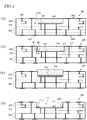
- FIG. 3 and FIG. 4 are process step cross-sectional views showing a method of prducing a multi-layer ceramic substrate. Referring to FIG. 2 , FIG. 3 and FIG. 4 , a method of prducing a multi-layer ceramic substrate of the present embodiment will be described. The following description is directed to an example where ceramic green sheets are laminated together to form one multi-layer ceramic substrate, but two or more multi-layer ceramic substrates may be formed.
- a ceramic material is prepared.
- a ceramic material including elements as described above is prepared and subjected to preliminary sintering at 700°C to 850°C, for example, as necessary, and pulverized into grains.
- a glass component powder, an organic binder, a plasticizer and a solvent are added to the ceramic material, thereby obtaining a slurry of the mixture.
- a powder of the conductive material described above is mixed with an organic binder and a solvent, etc., thereby obtaining a conductive paste.
- a layer of the slurry having a predetermined thickness is formed on a carrier film 250 by using a doctor blade method, a rolling (extrusion) method, a printing method, an inkjet application method, a transfer method, or the like, and the layer is dried.
- the dried slurry layer has a thickness of 20 ⁇ m to 200 ⁇ m, for example.
- the slurry layer is severed to obtain a plurality of ceramic green sheets 200 as shown in FIG. 3(a) (S11).
- via holes 201 are formed in the plurality of ceramic green sheets 200 by using a laser, a mechanical puncher, or the like, (S12), and the via holes 201 are filled with a conductive paste 202 by using a screen printing method (S13).
- a conductive paste is printed on the ceramic green sheets by using a screen printing, or the like, to form a wiring pattern 203 and a passive element pattern 204 on the ceramic green sheet 200 (S13).
- the diameter of the via holes 201 is 60 ⁇ m to 100 ⁇ m, for example, and the thickness of the wiring pattern 203 and the passive element pattern 204 is 5 ⁇ m to 35 ⁇ m, for example.
- the via pattern, the wiring pattern and the passive element pattern to be formed may vary for each green sheet depending on the position (level) of the ceramic green sheet 200.
- the plurality of ceramic green sheets 200 are classified into first ceramic green sheets 270 and second ceramic green sheets 260.
- the first ceramic green sheet 270 has a primary surface 270a to be the bottom surface of the cavity, and a region 206 to be the bottom surface of the cavity is located on the primary surface 270a.
- An electrode pattern 205 of a heat-radiating electrode may be formed in the region 206. No thermal expansion layer is formed on the second ceramic green sheet 260.
- a thermal expansion layer whose thickness increases when heated is prepared.
- the thermal expansion layer may have a sheet shape and may be cut into pieces of a desired shape, or a thermal expansion layer paste may be prepared and the thermal expansion layer may be formed by printing using screen printing, or the like.
- screen printing can be used, and patterns to be formed can easily be aligned with each other. In such a case, there are advantages such as being able to freely and easily determine the shape of the thermal expansion layer, being able to easily adjust the thickness thereof, etc.
- the thermal expansion layer includes a thermal expansion material that expands when heated.
- the expansion of the thermal expansion material increases the thickness of the thermal expansion layer, thereby displacing a portion of the ceramic green sheet that is located over the thermal expansion layer. It is preferred that the thickness of the thermal expansion layer increases when heated, and it is preferred that the thickness increases by a factor of 2 or more. That is, it is preferred that the expansion factor is 2 or more. It is more preferred that the thickness of the thermal expansion layer increases when heated by a factor of 2 or more and 12 or less, for example.
- the thermal expansion layer paste includes thermally-expansive microcapsules made of a thermoplastic resin that encapsulate a hydrocarbon that is in liquid form at normal temperature as the thermal expansion material, and includes organic materials such as a resin and a solvent.
- the thermally-expansive microcapsules have an average particle size of 5 ⁇ m to 50 ⁇ m, for example, and each include an outer shell made of a thermoplastic resin and a low boiling hydrocarbon filling the inside of the outer shell that is in liquid form at normal temperature. When heated at a temperature in the range of about 70°C to about 260°C, for example, the low boiling hydrocarbon evaporates and the outer shells soften at the same time, thereby forming independent hollow bubbles.
- the microcapsules expand.
- expansive microcapsules of various average particle sizes, thermal expansion start temperatures and maximum expansion temperatures are commercially available, and they can be used.
- the thermally-expansive microcapsule is selected so that the thickness of the thermal expansion layer reaches its maximum at a temperature that is higher than the heating temperature for final pressure-bonding to be described below and lower than the heating temperature for debindering.
- the thermal decomposition of the binder, and the like starts when the temperature increases past about 200°C.
- the thermally-expansive microcapsule to be selected for use in the thermal expansion layer is designed so that the thermal expansion layer expands at a temperature of 80°C or more and 200°C or less and reaches its maximum volume preferably at about 100°C to about 150°C. Then, it is possible to expand the thermal expansion layer without inhibiting the pressure-bonding of the ceramic green sheets during the final pressure-bonding process and while the binder is included in the green sheet laminate. Thus, it is possible to avoid the problem that the green sheet laminate becomes brittle because the binder is removed when forming the cavity, making it difficult to handle the green sheet laminate.
- the average particle size of the thermally-expansive microcapsules may influence the flatness of the bottom portion 111a of the cavity 111.
- thermally-expansive microcapsules having an average particle size that is as small as possible within the range described above, e.g., 10 ⁇ m, so that the unevenness of the bottom portion of the cavity 111 is reduced and the bottom portion becomes smooth.
- an unevenness improving material having a size smaller than the thermal expansion material so as to fill the gaps may be added to the thermal expansion layer paste.
- acrylic beads, or the like may be used as the unevenness improving material.
- the thermal expansion layer is arranged on the first ceramic green sheet 270.
- a thermal expansion layer 207 is formed in the region 206 to be the bottom surface of the cavity on the primary surface 270a of the first ceramic green sheet 270 (S14).
- a sheet-shaped thermal expansion layer 207 may be arranged, or the thermal expansion layer 207 may be formed by, for example, screen printing a paste.
- No thermal expansion layer is arranged on the second ceramic green sheet 260.
- a first ceramic green sheet 270 with a thermal expansion layer arranged thereon and at least one second ceramic green sheet 260 with no thermal expansion layer arranged thereon are prepared (S15).
- the thickness of the thermal expansion layer 207 is preferably 10 ⁇ m or more and 50 ⁇ m or less. If the thermal expansion layer is thinner than the thermally-expansive microcapsules, the thermally-expansive microcapsules sink into the ceramic green sheets, thereby deforming the ceramic green sheets. If the thermal expansion layer is too thick, it will inhibit the pressure-bonding between the ceramic green sheets.
- the thickness of the thermal expansion layer 207 is preferably greater than or equal to the average particle size of the thermally-expansive microcapsules.
- the multi-layer ceramic substrate 101 since the multi-layer ceramic substrate 101 includes one cavity 111, one thermal expansion layer 207 is arranged on the first ceramic green sheet 270 in FIG. 3(c) .
- the thermal expansion layer 207 is provided in each of the regions to be the bottom surfaces of the two or more independent cavities 111.
- the first and second ceramic green sheets 270 and 260 are sequentially laminated together with preliminary pressure-bonding therebetween, thereby forming a green sheet laminate (S16).
- the second ceramic green sheets 260 and the first ceramic green sheet 270 described above are sequentially laminated together with preliminary pressure-bonding therebetween so as to form a circuit as designed.
- the total number of layers of the first and second ceramic green sheets 270 and 260 in a green sheet laminate 280 is 4 to 20, for example.
- the procedure of preliminary pressure-bonding and lamination is in accordance with an ordinary method of prducing a multi-layer ceramic substrate.
- the lamination of the first and second ceramic green sheets 270 and 260 may be performed under a reduced pressure to make it easier to remove bubbles between sheets.
- one or more second ceramic green sheet 260 is laminated on the first ceramic green sheet 270 with the thermal expansion layer sandwiched therebetween.
- the second ceramic green sheet 260 may be arranged also under the first ceramic green sheet 270 to ensure the strength of the bottom of the cavity 111 to arrange the above-described circuit thereon.
- the green sheet laminate 280 is obtained as shown in FIG. 4(a) .
- the first ceramic green sheet 270 is arranged so that the primary surface 270a of the first ceramic green sheet 270 is located at a level (i.e., a height position in the lamination direction of the green sheet laminate) that is to be the bottom portion of the cavity.
- the multi-layer ceramic substrate 101 includes one cavity 111 in the present embodiment, it may include two or more cavities.
- two or more first ceramic green sheets 270 are arranged so that the primary surface 270a of each of the two or more first ceramic green sheets 270 is located at a level (i.e., a height position in the lamination direction of the green sheet laminate) that is to be the bottom portion of the corresponding cavity.
- the thermal expansion layer 207 is located in a region to be the bottom portion of a portion 208 to be the cavity.
- the portion 208 to be the cavity is a part of the second and/or first ceramic green sheet until it is separated by a groove 212 or the thermal expansion layer 207.
- an electrode pattern 209 and an electrode pattern 210 are formed on an upper surface 280a and a lower surface 280b, respectively, of the green sheet laminate 280 (S17).
- An overcoat material may be further arranged around the electrode pattern 209 and the electrode pattern 210.
- the first and second ceramic green sheets 270 and 260 of the green sheet laminate 280 are pressure-bonded together (S18).
- the green sheet laminate 280 is set in a frame, and the final pressure-bonding is performed by using a cold isostatic pressing (CIP) device, or the like.
- CIP cold isostatic pressing
- the entire green sheet laminate 280 may be heated during the final pressure-bonding so that the resin in the first and second ceramic green sheets 270 and 260 and the gluing agent in the conductive paste are softened to adhere with each other.
- the temperature at which the thermal expansion layer 207 starts expanding is dictated primarily by the characteristics of the thermally-expansive microcapsules included in the thermal expansion layer 207.
- the entire green sheet laminate 280 is heated in a temperature range of 60°C to 90°C.
- the groove 212 is formed on the green sheet laminate 280 for extracting the portion 208 to be the cavity (S19). Specifically, the groove 212 having a depth from the upper surface 280a along the lamination direction of the green sheet laminate 280 is formed so as to extend along the outline of the portion 208 to be the cavity as shown in FIG. 4(b) .
- the groove 212 may be formed by laser machining using YAG, or the like, or by punching using a blade shape of a knife cutter, or the like.
- the width of the groove 212 is preferably 10 ⁇ m to 200 ⁇ m, for example.
- the two opposing side surfaces that define the groove 212 may deform and come into contact with each other due to some external force after the formation of the groove 212. When the side surfaces come into contact with each other, it may become difficult to extract the portion 208 to be the cavity.
- the groove 212 may not reach the thermal expansion layer 207 but may have a depth with a margin M1 in the lamination direction of the green sheet laminate 280. That is, the bottom portion of the groove 212 and the thermal expansion layer 207 may be separated from each other by the margin M1 in the lamination direction.
- the groove 212 runs through the thermal expansion layer 207 and reaches a ceramic green sheet that is located below the thermal expansion layer 207, the groove 212 located below the thermal expansion layer 207 remains after sintering the green sheet laminate 280, even after the extraction of the portion 208 to be the cavity and the removal of the thermal expansion layer 207.
- Such a groove will lower the strength of the multi-layer ceramic substrate obtained by sintering.
- the groove 212 may have a margin M2 from the end portion of the thermal expansion layer 207 in the horizontal direction (the direction perpendicular to the lamination direction of the green sheet laminate 280 ).
- the groove 212 for extracting the portion 208 to be the cavity is provided in the green sheet laminate 280 in the present embodiment, the groove 212 may be absent when the depth of the cavity to be formed is as small as 50 ⁇ m or less.
- separation grooves for separating into individual substrates after sintering may be similarly formed at this point by using a knife cutter, or the like.
- the thermal expansion layer 207 is expanded by heat (S20). Specifically, the green sheet laminate 280 is held at a temperature such that the thickness of the thermal expansion layer 207 increases. This temperature is higher than the heating temperature for final pressure-bonding and lower than the heating temperature for debindering. For example, the green sheet laminate 280 is held at a temperature in the range of 110°C or more and less than 200°C for 1 min or more and 30 min or less. Preferably, the holding temperature is 150°C or less.
- the upper limit of the temperature for expanding the thermal expansion layer 207 is set to a temperature that is lower than the temperature at which the binder starts to be removed.
- the thermal expansion layer may be expanded after the debindering step or during the debindering step. In such a case, the thermal expansion layer may be expanded at a higher temperature.
- FIGS. 5(a) and 5(b) are schematic diagrams showing, on an enlarged scale, the vicinity of the end portion of the thermal expansion layer 207 for illustrating the expansion of the thermal expansion layer 207 and the separation of the portion 208 to be the cavity.
- different elements are scaled differently for the sake of illustration, and the figure does not represent the actual scale.
- the thermal expansion layer 207 is present in a state where thermal expansion layer microcapsules 207m and an organic material 207v are mixed together until the expansion of the thermal expansion layer 207 after the final pressure-bonding step.
- the margin M2 in the horizontal direction so that an end portion 207e of the thermal expansion layer 207 is located on the inner side of the opposite ends of the portion 208 to be the cavity in order to avoid a crack extending continuous from the bottom portion of the cavity.
- the margin M1 In the lamination direction of the green sheet laminate 280, there may be the margin M1 provided between the groove 212 and the thermal expansion layer 207.
- the thermal expansion layer microcapsules 207m are bonded to the portion 208 to be the cavity and the first ceramic green sheet 270 by means of the organic material 207v.
- the organic material 207v, the binder of the ceramic green sheets, etc. become soft, while the thermal expansion layer microcapsules 207m expand, thereby losing the adhesion. Therefore, peeling occurs between the thermal expansion layer microcapsules 207m and the portion 208 to be the cavity and between the thermal expansion layer microcapsules 207m and the first ceramic green sheet 270. Moreover, as the thermal expansion layer microcapsules 207m expand, the surrounding first and second ceramic green sheets are pushed apart from each other. As a result, the portion 208 to be the cavity and the first ceramic green sheet 270, which have been bonded together with the thermal expansion layer 207 interposed therebetween, peel off and come off the thermal expansion layer 207.
- the thickness of the thermal expansion layer 207 increases as shown in FIG. 4(c) .
- the portion 208 of the ceramic green sheet to be the cavity remains connected to the rest in a portion 211 where the margin M1 and the margin M2 are provided.
- a shear stress acts on the portion 211 due to the displacement of the portion 208 to be the cavity and the stress from the expansion of the thermal expansion layer microcapsules 207m.
- the cavity 111 is formed in the green sheet laminate 280 (S21).
- the side surface of the portion 208 to be the cavity is completely separated from the green sheet laminate 280.
- the portion 208 to be the cavity drops off the green sheet laminate 280 by virtue of its own weight, thus obtaining a green sheet laminate 290 provided with the cavity 111 having an opening on the upper surface 280a. If the portion 208 to be the cavity does not easily drop by virtue of its own weight because of the groove width being small, the portion 208 to be the cavity may be removed by using a tape, a suction head, or the like.
- a part or whole of the thermal expansion layer 207 may come off together with the portion 208 to be the cavity, or the entire thermal expansion layer 207 may remain stuck on the bottom of the cavity 111. That is, a part or whole of the thermal expansion layer 207 may be removed together with the portion 208 to be the cavity. If a part or whole of the thermal expansion layer 207 remains in the green sheet laminate 280, most of it disappears in the debindering step to be described below. The thermal expansion layer 207 that does not disappear in the debindering step can be made to disappear in the sintering step.
- the thermal expansion layer includes a portion that remains after the sintering step as described above, a pretreatment of cleaning a thermal expansion material, etc., may be performed before forming the thermal expansion layer by using a thermal expansion layer paste including the thermal expansion material.
- the crack 213 occurs in a slant direction with respect to the lamination direction of the ceramic green sheets, and the burrs 208b occur on the bottom portion 111a of the cavity 111.
- the length op2 of a flat bottom portion 111b is shorter than the length of the opening op1 of the cavity 111, as shown in FIG. 4(d) .
- the binder is removed from the green sheet laminate 290 having the cavity 111 (S22). Specifically, organic components such as a resin and a solvent included in the green sheet laminate 290 are heated and removed. For example, it is held at a temperature in the range of 200°C or more and 600°C or less for 120 min or more and 600 min or less.
- the holding temperature may be constant or may be varied.
- the green sheet laminate 290 may be heated up to 500°C, and then it may be cooled gradually or the holding temperature may be lowered gradually.
- the resin, the solvent and the thermal expansion layer 207 included in the green sheet laminate 290 disappear (evaporate).
- the thermal expansion layer 207 disappears at a temperature in the range of about 350°C to 600°C.
- the temperature range is the same as the debindering temperature range, it is possible to expand the thermal expansion layer during the debindering step, as described above, and to cause most of the remaining thermal expansion layer to disappear during the debindering after the cavity is formed. Moreover, if there remain traces of the thermal expansion material on the bottom surface of the cavity formed, a material that disappears in this temperature range can be used, as an unevenness improving material, to fill the gaps in the thermal expansion material.
- the unevenness improving material may be acrylic beads, or the like.
- This debindering step may be performed successively after the step of expanding the thermal expansion layer, and the cavity may be formed after the debindering step. By successively performing the two steps, it is possible to shorten the manufacturing process.
- the thermal expansion layer may be expanded after the debindering step to remove the portion to be the cavity, thereby forming the cavity.
- the green sheet laminate is held at a temperature such that the thermal expansion layer does not expand in the debindering step.
- the debindered green sheet laminate 290 is sintered (S23). Specifically, the green sheet laminate 290 is held at a sintering temperature for the ceramic included in the ceramic green sheet, thereby sintering the ceramic. For example, it is held at a temperature in the range of 850°C or more and 940°C or less for 100 min or more and 180 min or less. Thus, it is possible to obtain a multi-layer ceramic substrate shown in FIG. 1(b) .
- This sintering step may be performed successively after the debindering step.
- the green sheet laminate with a cavity formed therein is held at a temperature in the range of 200°C or more and 600°C or less for 120 min or more and 600 min or less, and then held at a temperature in the range of 850°C or more and 940°C or less for 100 min or more and 180 min or less.
- the holding temperature may be constant or may be varied.
- the green sheet laminate 290 may be heated up to 200°C and slowly heated up to 600°C, and then it may be heated to a temperature in the range of 850°C or more and 940°C or less.
- the green sheet laminate forms a large substrate that is a collection of multi-layer ceramic substrates 101, it is possible to obtain a plurality of multi-layer ceramic substrates by severing the large substrate, obtained by sintering, along separation grooves.
- the thickness of the thermal expansion layer increases when heated, thereby displacing a portion of the green sheet laminate to be the cavity.
- the thermal expansion layer is thin before being heated, and it does not inhibit the adhesion between two ceramic green sheets when it is interposed between the ceramic green sheets. Therefore, it is possible to prevent ceramic green sheets from being shifted from each other when laminating the ceramic green sheets together to form a green sheet laminate and when forming a groove along the outline of the cavity.
- it is possible to maintain a high formability of the green sheet laminate e.g., it is possible to increase the adhesion between ceramic green sheets in the green sheet laminate and to ensure a good flatness of the cavity bottom surface.
- the thickness of the thermal expansion layer increases significantly, thereby displacing the portion to be the cavity of the green sheet laminate. Therefore, even if the groove along the outline of the cavity is not completely connected to the thermal expansion layer, the shear stress due to the displacement causes a crack in the ceramic green sheet, thereby separating the portion to be the cavity from the green sheet laminate. The shear stress is unlikely to cause a crack in an unintended portion. Therefore, even with an alignment error taken into account, it is possible to reliably separate the portion to be the cavity from the green sheet laminate with a high yield. Moreover, since it is possible to check whether the cavity has been formed properly before sintering, it is possible to exclude defective prodcuts before sintering. Thus, it is possible to provide a method of prducing a multi-layer ceramic substrate with a good mass productivity and with a high yield.
- a multi-layer ceramic substrate may include a plurality of cavities having the same depth, or may include a plurality of cavities having different depths.
- a multi-layer ceramic substrate may include a cavity having a plurality of bottom surfaces of different heights.
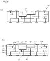
- a multi-layer ceramic substrate 102 may include a cavity 111' having a first bottom portion 111a and a second bottom portion 111a' at different heights. While the second bottom portion 111a' is located deeper than the first bottom portion 111a in the cavity 111' in the present embodiment, the second bottom portion 111a' may be located shallower than the first bottom portion 111a.
- a groove 212' and the groove 212 are formed at positions to be the side surface of the cavity 111'. Moreover, it is preferred that the groove 212' is provided at the boundary between the region 206 and the region 206' so as to reach the vicinity of the primary surface 270a' of the third ceramic green sheet 270'.
- the multi-layer ceramic substrate 102 can be manufactured with the other conditions being equal to those of the method described above. In this case, the thickness of the thermal expansion layer 207 as expanded may be different from the thickness of the thermal expansion layer 207' as expanded.
- the multi-layer ceramic substrate may include a cavity having three or more bottom portions at different levels.
- three first ceramic green sheets 270 including thermal expansion layers at different positions from each other are prepared, and these three first ceramic green sheets 270 are arranged in the green sheet laminate so as to be at different levels from each other.
- the cavity 111' may have one second bottom portion 111a', and two first bottom portions 111a located with the second bottom portion 111a' sandwiched therebetween.
- a first ceramic green sheet 270 including two thermal expansion layers 207 arranged at positions corresponding to the two first bottom portions 111a there are prepared a first ceramic green sheet 270 including two thermal expansion layers 207 arranged at positions corresponding to the two first bottom portions 111a, and a third ceramic green sheet 270' including a thermal expansion layer 207' arranged at a position corresponding to the second bottom portion 111a'.
- the first ceramic green sheet 270 and the third ceramic green sheet 270' are laminated together so as to be at different levels from each other.
- FIG. 8(a) and FIG. 8(b) are a cross-sectional view and a plan view, respectively, of a multi-layer ceramic substrate 104.
- the multi-layer ceramic substrate 104 includes an electrode 114' that is larger than the bottom portion 111a of the cavity 111.
- the conductive via 120 is connected to the electrode 114', and the conductive via 120 is connected to the heat-radiating electrode 115 provided on the lower surface 110b of the ceramic sinter 110, for example.
- the electrode 114' is used as a heat-radiating electrode or a ground electrode for an electronic component arranged in the cavity 111, for example.
- FIG. 8(a) shows the electrode 114' as if a portion thereof that is exposed as the bottom portion 111a of the cavity 111 and a portion thereof that is buried in the ceramic sinter 110 were forming the same plane.
- the thermal expansion layer 207 is arranged only on a portion (to be the cavity 111 ) of the electrode pattern 205 to be the electrode 114'. Therefore, when forming the green sheet laminate, a portion of the electrode pattern 205 to be the cavity 111 may possibly be depressed by being pressed by the thermal expansion layer 207.
- the electrode 114' of the multi-layer ceramic substrate 104 may include a depressed portion in an area where it is exposed as the bottom portion 111a of the cavity 111.
- the groove 212 for forming the cavity 111 is located above the electrode pattern 205 during the manufacturing process, as shown in FIG. 9 .
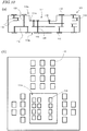
- FIG. 10(a) and FIG. 10(b) are a cross-sectional view and a plan view, respectively, of a multi-layer ceramic substrate 105.
- the multi-layer ceramic substrate 105 includes a plurality of pad electrodes 116 on the bottom portion 111a of the cavity 111.
- the conductive vias 120 are connected to the pad electrodes 116, and the conductive vias 120 are connected to the wiring pattern 119, the passive element pattern 118, etc.
- an electronic component such as an integrated circuit can be connected by flip-chip bonding in the cavity 111. Therefore, there is no need to connect bonding wires to an active element accommodated in the cavity 111 as shown in FIG. 1 , etc., and it is possible to reduce the height of the multi-layer ceramic substrate 105 with an electronic component mounted thereon.
- another electronic component, another multi-layer ceramic substrate, or the like can be arranged on the multi-layer ceramic substrate 105.
- FIG. 11(a) and FIG. 11(b) are a cross-sectional view and a plan view, respectively, of a multi-layer ceramic substrate 106.
- the multi-layer ceramic substrate 106 is different from the multi-layer ceramic substrate 104 shown in FIG. 10 in that the multi-layer ceramic substrate 106 further includes an electrode 117 that is located below the side surface of the cavity 111, extending along the periphery of the bottom portion 111a.
- the groove 212 for forming the cavity 111 is located over the pattern of the electrode 117. Therefore, with the multi-layer ceramic substrate 106, the burrs 208b are unlikely to occur on the bottom portion 111a of the cavity 111, and the burrs 208b, even if produced, will be small.
- the cavity forming step is performed after the step of expanding the thermal expansion layer in the embodiment described above, the cavity forming step may be performed during the step of expanding the thermal expansion layer or during the debindering step.
- the expansion step or during the debindering step means that the cavity is formed while the green sheet laminate is held under the condition for the expansion step or the condition for the debindering step.
- a thermal expansion layer paste was prepared, and it was confirmed that the thermal expansion layer exhibited a thickness change sufficient for the formation of the cavity at a desired temperature.
- Ceramic green sheets were produced by forming a ceramic material including Al, Si and Sr as its main components and Ti, Bi, Cu, Mn, Na and K as its sub-components into a sheet shape.
- Thermally-expansive microcapsules (F, FN series from Matsumoto Yushi-Seiyaku Co., Ltd.) having average particle sizes and expansion start temperatures shown in Table 1 were prepared as thermal expansion materials.
- TMC-108 (from Tanaka Kikinzoku Kogyo K.K.) was used as a vehicle, and the thermally-expansive microcapsules and the vehicle were mixed together at a weight ratio of 1:9 to produce a paste.
- the obtained paste was applied on a PET film so that the thickness as dried is about 0.1 mm and then dried, thereby obtaining samples of thermal expansion layers.
- a plurality of samples were produced using the thermal expansion materials of Samples 1 to 3.
- the produced samples were heated at a temperature of 70°C to 130°C, and the change in the thickness of each sample was measured by using a micrometer, and the thickness change of the sample was calculated.
- the results are shown in FIG. 12 .
- the horizontal axis represents the temperature at which heating was done, and the vertical axis represents the thickness change (expansion factor) with respect to the thickness before being heated.
- each sample expands at about 100°C to about 110°C, and the thickness thereof increases by a factor of about 2 to about 5 at 130°C.
- the temperature range is between the temperature of the final pressure-bonding and the temperature of the debindering in the manufacturing process of the multi-layer ceramic substrate.
- the amount of thickness change of the thermal expansion layer that is needed for forming a cavity without forming a groove was examined. Ceramic green sheets having a thickness of 110 ⁇ m were prepared, and six of them were layered together to form a ceramic green sheet laminate. The size of the cavity was 25 mm long, 25 mm wide and 0.1 mm deep.
- the thermal expansion layer paste of Sample 1 described above was applied on a ceramic green sheet by using a screen printing method. The thickness of the thermal expansion layer was 0.01 mm, as measured by observing the cross section of the produced sheet laminate with a microscope. In order to vary the amount of thickness change, the heating temperature when expanding the thermal expansion layer was adjusted in accordance with FIG. 12 .
- the percentage of proper extraction refers to the percentage with which the portion corresponding to the cavity was extracted properly because of the thickness change of the thermal expansion layer. That is, for the following results, a study was conducted to determine a predetermined range of the amount of thickness change before and after heating the thermal expansion layer for forming the cavity, without forming, in the green sheet laminate, a groove that has the depth of the cavity and that defines the outline of the cavity.
- the thickness of the thermal expansion layer preferably increases by a factor of 2 or more and 4 or less by being heated.
- FIGS. 13(a) and 13(b) are optical microscopic images before and after the thermal expansion layer is heated, respectively, for a sample that was obtained by laminating and pressure-bonding six layers of ceramic green sheets each having a thickness of 110 ⁇ m, wherein the depth of the cavity was 0.2 mm and the amount of thickness change was 6 times. While it can be seen from FIG. 13(a) that the thickness of the thermal expansion layer before being heated was about 10 ⁇ m, it can be seen from FIG. 13(b) that the thickness of the thermal expansion layer after being heated was about 50 ⁇ m.
- a multi-layer ceramic substrate was manufactured, in which a cavity was formed under the following condition.
- a ceramic material including Al, Si and Sr as its main components and Ti, Bi, Cu, Mn, Na and K as its sub-components was prepared.
- a plurality of ceramic green sheets were obtained as described above using the ceramic material prepared.
- via holes were formed in the obtained ceramic green sheets by using a laser puncher, and screen printing was used to fill the via holes with a conductive paste and to form wiring patterns.
- a material including Ag as a conductive material was used as the conductive paste.
- a thermal expansion layer was formed in a region of the first ceramic green sheet to be the bottom surface of the cavity. The thermal expansion layer was formed by a screen printing method using a thermal expansion layer paste so that the thickness as dried would be 10 ⁇ m.
- thermally-expansive microcapsules F, FN series from Matsumoto Yushi Kogyo
- acrylic beads from Sekisui Plastics Co., Ltd.
- the obtained first and second ceramic green sheets were successively laminated together by repeating the operation of preliminary pressure-bonding one of the first and second ceramic green sheets and peeling off the carrier film to obtain a green sheet laminate including 4 to 20 layers of ceramic green sheets, specifically, seven layers of ceramic green sheets, each having a thickness of 80 ⁇ m, laminated together. Then, the green sheet laminate was subjected to final pressure-bonding at 17 MPa while being heated to 85°C.
- a groove having a depth of 180 ⁇ m was formed along the outline of the portion to be the cavity by using a chisel blade shape.
- the thermal expansion layer of the grooved green sheet laminate was heated to 130°C and held for 15 min.
- the thickness of the thermal expansion layer was increased and the portion to be the cavity was displaced.
- the displaced portion to be the cavity was easily extracted by a tape, thereby forming the cavity.
- grooves to be used for separation after sintering were formed.
- the green sheet laminate with the cavity formed therein and with separation grooves formed therein was subjected to the debindering step and the sintering step in the range of conditions described above by using a continuous furnace.
- a multi-layer ceramic substrate having a cavity was obtained. It was confirmed that although a part of the expanded thermal expansion layer remained on the bottom portion of the cavity when the cavity was formed in the green sheet laminate, most of it had disappeared after the sintering step. Moreover, even traces of thermal expansion layer microcapsules did not remain on the bottom surface of the cavity after sintering.
- the thickness of the co-fired multi-layer ceramic substrate and the depth of the cavity were varied so as to check whether a small cavity can be produced.
- multi-layer ceramic substrates were produced whose thicknesses would be 325 ⁇ m, 650 ⁇ m and 1300 ⁇ m, after being fired.
- the size of the cavity was 1.3 mm ⁇ 1.3 mm, 2.3 mm ⁇ 2.3 mm. Whether the cavity can be formed was checked while setting the depth of the cavity to 100 ⁇ m, 150 ⁇ m, 200 ⁇ m, 250 ⁇ m and 300 ⁇ m. The results are shown in Table 3.
- ⁇ indicates that a cavity having a desirable shape was formed.
- ⁇ indicates that the extraction of the cavity was not easy, and the shape of the cavity formed did not have a sufficiently good finish.
- ⁇ indicates that a crack occurred on the bottom portion of the cavity.
- the size in the horizontal direction of the burrs 208b produced on the bottom portion 111a of the cavity 111 was examined when producing a multi-layer ceramic substrate while setting, to various values, the margin M1 in the vertical direction and the margin M2 in the horizontal direction between the end portion of the groove 212 and the end portion of the thermal expansion layer 207.
- a multi-layer ceramic substrate that includes a cavity having a 2.3 mm by 2.3 mm rectangular opening and has an electrode on the bottom portion of the cavity as shown in FIG. 8 (hereinafter, a "multi-layer ceramic substrate with an electrode”) and a multi-layer ceramic substrate that includes a cavity having a 2.3 mm by 2.3 mm rectangular opening and has no electrode on the bottom portion of the cavity (hereinafter, a "multi-layer ceramic substrate without an electrode”) were produced.
- the depths of the cavities were 200 ⁇ m and 300 ⁇ m.
- the results are shown in Tables 4 and 5.
- the margin M1 in the vertical direction and the margin M2 in the horizontal direction are as shown in Tables 4 and 5.
- the size of the burr 208b represents the sum of the lengths of the burrs 208b on the opposite sides for the width direction and for the longitudinal direction, and Tables 4 and 5 show an average value of the burrs 208b in the width direction and the longitudinal direction.
- the margin M1 being -50 indicates an over-cut, i.e., formation of a groove that is 50 ⁇ m deeper than the thermal expansion layer. Such samples for the multi-layer ceramic substrate with an electrode were not produced because the electrode would then be severed.
- the burrs 208b can generally be made smaller with a multi-layer ceramic substrate with an electrode. There is also a tendency that the burrs 208b become longer as the cavity is deeper (Table 5). It can be seen from these results that it is possible to adjust the length of the burrs 208b by varying the margins M1 and M2. Specifically, it was found that it is possible to make the length of the burrs to be 250 ⁇ m or less by adjusting the margins M1 and M2, and with a multi-layer ceramic substrate with an electrode, it is possible to make the length of the burrs 208b to be about 100 ⁇ m or less by setting suitable margins M1 and M2. Also, it was found that with a multi-layer ceramic substrate without an electrode, it is possible to make the length of the burrs 208b to be about 150 ⁇ m or less by setting suitable margins M1 and M2.
- the method of prducing a multi-layer ceramic substrate of the present disclosure can suitably be used in a multi-layer ceramic substrate having a cavity that is suitable for various applications.
Landscapes
- Engineering & Computer Science (AREA)
- Manufacturing & Machinery (AREA)
- Microelectronics & Electronic Packaging (AREA)
- Chemical & Material Sciences (AREA)
- Ceramic Engineering (AREA)
- Physics & Mathematics (AREA)
- Fluid Mechanics (AREA)
- Mechanical Engineering (AREA)
- Inorganic Chemistry (AREA)
- Production Of Multi-Layered Print Wiring Board (AREA)
- Devices For Post-Treatments, Processing, Supply, Discharge, And Other Processes (AREA)
- Geometry (AREA)
- Compositions Of Oxide Ceramics (AREA)
Abstract
Description
- The present invention relates to a method of prducing a multi-layer ceramic substrate having a cavity.
- Multi-layer ceramic substrates have been widely used as wiring substrates for use in various electronic devices such as communication devices. Using a multi-layer ceramic substrate, it is possible to incorporate passive elements, such as capacitors, coils and transmission paths, into the substrate and implement electronic components on the surface of the substrate, thus realizing a small module. Moreover, in recent years, a cavity is provided in a multi-layer ceramic substrate and a semiconductor IC is accommodated in the cavity so as to achieve a low profile of the module as a whole and to highly integrate and combine functions together.
- Such a multi-layer ceramic substrate with a cavity is commonly produced by laminating and pressure-bonding together a ceramic green sheet having an opening corresponding to the cavity and a ceramic green sheet having no opening, and then sintering the ceramic green sheets. However, a ceramic green sheet having an opening is likely to deform when pressure-bonded.
- In view of this, Patent Document No. 1 discloses a method of prducing a multi-layer ceramic substrate with a cavity, wherein a ceramic green sheet laminate is produced by providing a peel-off layer sandwiched at a position to be the bottom of the cavity, making a slit that reaches the peel-off layer from one primary surface of the laminate before or after the preliminary sintering (debindering process), removing a portion of the green sheet that corresponds to the cavity, and then sintering the laminate.
- Patent Document No. 2 discloses a method of prducing a multi-layer ceramic substrate with a cavity, wherein a ceramic green sheet laminate is produced by providing a burn-out material layer sandwiched at a position to be the bottom of the cavity, and grooving the laminate from one primary surface thereof before or after co-firing the laminate, so that the burn-out material layer is burnt out in the co-firing process, thus producing an internal space, whereby the cavity portion can be removed.
-
- [Patent Document No. 1] Japanese Laid-Open Patent Publication No.
2001-358247 - [Patent Document No. 2] Japanese Laid-Open Patent Publication No.
2003-273267 - However, as a result of a study by the present inventor, it was found that it may not be easy in some cases to form a cavity by the methods of Patent Document Nos. 1 and 2. It is an object of the present invention to provide a method of prducing a multi-layer ceramic substrate which has a good mass productivity and with which it is possible to easily form a cavity,
- A method of prducing a multi-layer ceramic substrate of the present invention includes the steps of: (A) preparing a first ceramic green sheet with a thermal expansion layer arranged thereon, and at least one second ceramic green sheet with no thermal expansion layer arranged thereon; (B) laminating the first and second ceramic green sheets with the thermal expansion layer sandwiched therebetween, thereby obtaining a green sheet laminate; (C) pressure-bonding together the first ceramic green sheet and the at least one second ceramic green sheet of the green sheet laminate; (D) heating and thereby expanding the thermal expansion layer at least in a thickness direction in the pressure-bonded green sheet laminate; (E) extracting a portion of the green sheet laminate that has been displaced by the expansion of the thermal expansion layer, thereby forming a cavity in the green sheet laminate; and (F) sintering the green sheet laminate with the cavity formed therein.
- In the step (D), the thermal expansion layer may be held at a temperature higher than a temperature for pressure-bonding in the step (C).
- The thermal expansion layer may include a thermal expansion material whose thickness increases by a factor of 2 or more by being heated.
- The thermal expansion layer may be a layer of a paste including thermally-expansive microcapsules made of a thermoplastic resin that encapsulate a hydrocarbon that is in liquid form at normal temperature.
- The method may further include, between the step (C) and the step (D), a step of forming, in the green sheet laminate, a groove that has a depth of the cavity of the green sheet laminate and defines an outline of the cavity.
- The thermal expansion layer may be removed in the step (E).
- In the step (A), a third ceramic green sheet with another thermal expansion layer arranged thereon may be prepared in a region different from the first ceramic green sheet; in the step (B), the first to third ceramic green sheets may be laminated together so that the thermal expansion layers are sandwiched therebetween, thereby obtaining the green sheet laminate; in the step (D), the other thermal expansion layer may be heated to be expanded at least in the thickness direction; and in the step (E), a portion of the green sheet laminate that has been displaced by the expansion of the other thermal expansion layer may be extracted.
- The method may further include, between the step (E) and the step (F), a step (G) of removing a binder from the green sheet laminate.
- In the step (D), the thermal expansion layer may be held at a temperature that is higher than a temperature for pressure-bonding in the step (C) and lower than a temperature for binder removing in the step (G).
- In the step (A), at least one of the first ceramic green sheet and the second ceramic green sheet may include a pattern to be internal wiring, an inductor, a condenser, a stripline or an internal resistor.
- In the step (A), the first ceramic green sheet may further include a conductor pattern located between the thermal expansion layer and the first ceramic green sheet.
- In the step (A), at least one of the first ceramic green sheet and the second ceramic green sheet may further include a via hole and a conductive paste that fills the via hole.
- According to the present invention, there is provided a method of prducing a multi-layer ceramic substrate which has a good mass productivity and with which it is easy to extract a portion corresponding to the cavity.
-
- [
FIG. 1 ] (a) is a perspective view showing an example of a multi-layer ceramic substrate of the present embodiment, (b) is a cross-sectional view taken alongline 1B-1B of (a), and (c) is a perspective view showing an example of a multi-layer ceramic substrate with a semiconductor IC chip mounted in the cavity. - [
FIG. 2 ] A flow chart showing a method of prducing a multi-layer ceramic substrate of the present embodiment. - [
FIG. 3 ] (a) to (c) are process step cross-sectional views showing a method of prducing a multi-layer ceramic substrate of the present embodiment. - [
FIG. 4 ] (a) to (d) are process step cross-sectional views showing the method of prducing a multi-layer ceramic substrate of the present embodiment. - [
FIG. 5 ] (a) and (b) are schematic diagrams showing, on an enlarged scale, the vicinity of an end portion of a thermal expansion layer for illustrating the expansion of the thermal expansion layer and the separation of the portion to be the cavity. - [
FIG. 6 ] (a) is a cross-sectional view showing another example of a multi-layer ceramic substrate of the present embodiment, and (b) is a cross-sectional view showing one step of a method of prducing the multi-layer ceramic substrate of (a). - [
FIG. 7 ] (a) is a cross-sectional view showing another example of a multi-layer ceramic substrate of the present embodiment, and (b) is a cross-sectional view showing one step of a method of prducing the multi-layer ceramic substrate of (a). - [
FIG. 8 ] (a) is a cross-sectional view showing another example of a multi-layer ceramic substrate of the present embodiment, and (b) is a plan view of (a). - [
FIG. 9 ] A cross-sectional view showing one step of a method of prducing the multi-layer ceramic substrate shown inFIG. 8 . - [
FIG. 10 ] (a) is a cross-sectional view showing another example of a multi-layer ceramic substrate of the present embodiment, and (b) is a plan view of (a). - [
FIG. 11 ] (a) is a cross-sectional view showing another example of a multi-layer ceramic substrate of the present embodiment, and (b) is a plan view of (a). - [
FIG. 12 ] A graph showing the relationship between the temperature of the thermal expansion layer and the expansion factor for samples shown in Table 1. - [
FIG. 13 ] (a) and (b) are optical microscopic images, before and after the expansion of the thermal expansion layer, of a green sheet laminate of a sample produced by a method of prducing a multi-layer ceramic substrate of the present embodiment. - The present inventor made an in-depth study on the methods for manufacturing a multi-layer ceramic substrate disclosed in Patent Document Nos. 1 and 2. According to the methods of Patent Document Nos. 1 and 2, there is a need to form a slit or a groove reaching a peel-off layer or a burn-out layer in order to extract a portion of a green sheet corresponding to the cavity or a portion of a sinter corresponding to the cavity. It is difficult to separate the portion corresponding to the cavity unless the slit or groove is aligned with the position of the peel-off layer or burn-out layer and reliably extends to reach the peel-off layer or burn-out layer. Particularly, with the method of Patent Document No. 2, whether the portion corresponding to the cavity can be separated is known after the co-firing process, and it is therefore necessary to perform the manufacturing process up to the co-firing process even if it is a defective product.
- According to the method of Patent Document No. 1, since the peel-off layer is made of a material such that the ceramic green sheet can be peeled off easily, a green sheet laminate with the peel-off layer interposed therein will have an insufficient adhesion between the peel-off layer and the ceramic green sheet. Therefore, the pressure-bonded green sheet laminate may have an insufficient form stability or a green sheet may be shifted when forming a slit. With such problems described above, it may be difficult in some cases to stably manufacture a multi-layer ceramic substrate, thereby posing problems particularly in view of mass productivity. In view of such problems, the present inventor arrived at a novel method of prducing a multi-layer ceramic substrate. One embodiment of a multi-layer ceramic substrate and a method of prducing a multi-layer ceramic substrate of the present invention will now be described in detail. Note that a green sheet laminate as used in the description below is what is obtained by laminating first and second ceramic green sheets together, and every state from lamination until sintering is defined as a green sheet laminate, irrespective of the order and number of the sheets, the positions and number of thermal expansion layers, and the presence/absence of internal wiring or elements arranged inside the laminate.
-
FIG. 1(a) is a perspective view showing an example of a multi-layer ceramic substrate of the present embodiment, andFIG. 1(b) shows a cross section taken alongline 1B-1B ofFIG. 1(a) . - A multi-layer
ceramic substrate 101 includes aceramic sinter 110 having anupper surface 110a and alower surface 110b. Theupper surface 110a is provided with acavity 111 for accommodating an electronic component such as a semiconductor IC chip. Thecavity 111 has a recessed shape having an opening on theupper surface 110a. Oneelectrode 112 or a plurality ofelectrodes 112 may be provided on theupper surface 110a. Oneelectrode 113 or a plurality ofelectrodes 113 may be provided on thelower surface 110b. A heat-radiatingelectrode 114 is provided on abottom portion 111a of thecavity 111 in order to radiate heat from the semiconductor IC accommodated in thecavity 111. While the multi-layerceramic substrate 101 shown inFIG. 1 includes onecavity 111, the multi-layer ceramic substrate may include two or more cavities. In this case,bottom portions 111a may be at the same level or at different levels in two ormore cavities 111, as will be described below. - A
passive element pattern 118 and a conductive via 120 and awiring pattern 119 may be provided inside theceramic sinter 110. Thepassive element pattern 118 may have a conductivity or a predetermined resistance value, for example, and may form internal wiring, an inductor, a condenser, a stripline, an internal resistor, or the like. - The
wiring pattern 119 is made of a conductive thin-layer pattern that is generally parallel to theupper surface 110a and thelower surface 110b. The conductive via 120 is made of a via hole extending in a direction connecting between theupper surface 110a and thelower surface 110b, and a columnar-shaped conductor filling the via hole. Thewiring pattern 119 and the conductive via 120 are connected to thepassive element pattern 118, thewiring pattern 119, theelectrode 112, theelectrode 113, theelectrode 114, etc., thereby forming a predetermined circuit. - As shown in
FIG. 1(b) , the conductive via 120 connected to the heat-radiatingelectrode 114 may reach thelower surface 110b as a radiator. A heat-radiatingelectrode 115 that is connected to the conductive via 120 connected to the heat-radiatingelectrode 114 may be further provided on thelower surface 110b. - The multi-layer
ceramic substrate 101 may be a low temperature co-fired ceramic (LTCC) substrate or a high temperature co-fired ceramic (HTCC) substrate. A ceramic material and a conductive material suitable for the sintering temperature, the application, etc., are used for theceramic sinter 110, thepassive element pattern 118, thewiring pattern 119, theelectrode 112, theelectrode 113 and theelectrode 114. When the multi-layerceramic substrate 101 is a low temperature co-fired multi-layer ceramic substrate, a ceramic material and a conductive material that can be sintered in a temperature range of about 800°C to about 1000°C are used. For example, the ceramic material used may be a ceramic material including Al, Si and Sr as its main components and Ti, Bi, Cu, Mn, Na and K as its sub-components, a ceramic material including Al, Si and Sr as its main components and Ca, Pb, Na and K as its sub-components, a ceramic material including Al, Mg, Si and Gd, and a ceramic material including Al, Si, Zr and Mg. The conductive material used may be a conductive material including Ag or Cu. The dielectric constant of the ceramic material is about 3 to about 15. When the multi-layerceramic substrate 101 is a high temperature co-fired multi-layer ceramic substrate, a ceramic material including Al as its main components, and a conductive material including W (tungsten) or Mo (molybdenum) may be used. - There is no particular limitation on the size of the multi-layer
ceramic substrate 101. The multi-layerceramic substrate 101 may be produced in a size that is suitable for the application, the number of passive elements included therein, the circuit scale, the size and number ofcavities 111, etc. -
FIG. 1(c) shows a state where a semiconductor IC chip and a capacitor are mounted on the multi-layerceramic substrate 101. As shown inFIG. 1(c) , asemiconductor IC chip 151 is arranged in thecavity 111. For example, thesemiconductor IC chip 151 is secured, facing up, by a solder, a heat-conductive adhesive, etc.Electrodes 151a of thesemiconductor IC chip 151 and theelectrodes 112 of the multi-layerceramic substrate 101 are connected together by bondingwires 153. A passive element or an active element that can be surface-mounted, such as acapacitor 152, for example, may be connected to theelectrode 112 by a solder. Although not shown in the figures, thesemiconductor IC chip 151 may be mounted, facing down, in thecavity 111. In such a case, electrodes corresponding to the electrodes of thesemiconductor IC chip 151 are provided on the bottom surface of thecavity 111, and the electrodes on the bottom surface of thecavity 111 are connected to the electrodes of thesemiconductor IC chip 151 by reflow soldering, or the like. - A method of prducing a multi-layer ceramic substrate will be described.
FIG. 2 is a flow chart showing a method of prducing a multi-layer ceramic substrate.FIG. 3 andFIG. 4 are process step cross-sectional views showing a method of prducing a multi-layer ceramic substrate. Referring toFIG. 2 ,FIG. 3 andFIG. 4 , a method of prducing a multi-layer ceramic substrate of the present embodiment will be described. The following description is directed to an example where ceramic green sheets are laminated together to form one multi-layer ceramic substrate, but two or more multi-layer ceramic substrates may be formed. - First, a ceramic material is prepared. A ceramic material including elements as described above is prepared and subjected to preliminary sintering at 700°C to 850°C, for example, as necessary, and pulverized into grains. A glass component powder, an organic binder, a plasticizer and a solvent are added to the ceramic material, thereby obtaining a slurry of the mixture. A powder of the conductive material described above is mixed with an organic binder and a solvent, etc., thereby obtaining a conductive paste.
- A layer of the slurry having a predetermined thickness is formed on a
carrier film 250 by using a doctor blade method, a rolling (extrusion) method, a printing method, an inkjet application method, a transfer method, or the like, and the layer is dried. The dried slurry layer has a thickness of 20 µm to 200 µm, for example. The slurry layer is severed to obtain a plurality of ceramicgreen sheets 200 as shown inFIG. 3(a) (S11). - As shown in
FIG. 3(b) , in accordance with a circuit to be formed in the multi-layer ceramic substrate, viaholes 201 are formed in the plurality of ceramicgreen sheets 200 by using a laser, a mechanical puncher, or the like, (S12), and the via holes 201 are filled with aconductive paste 202 by using a screen printing method (S13). A conductive paste is printed on the ceramic green sheets by using a screen printing, or the like, to form awiring pattern 203 and apassive element pattern 204 on the ceramic green sheet 200 (S13). The diameter of the via holes 201 is 60 µm to 100 µm, for example, and the thickness of thewiring pattern 203 and thepassive element pattern 204 is 5 µm to 35 µm, for example. The via pattern, the wiring pattern and the passive element pattern to be formed may vary for each green sheet depending on the position (level) of the ceramicgreen sheet 200. The plurality of ceramicgreen sheets 200 are classified into first ceramicgreen sheets 270 and second ceramicgreen sheets 260. The first ceramicgreen sheet 270 has aprimary surface 270a to be the bottom surface of the cavity, and aregion 206 to be the bottom surface of the cavity is located on theprimary surface 270a. Anelectrode pattern 205 of a heat-radiating electrode may be formed in theregion 206. No thermal expansion layer is formed on the second ceramicgreen sheet 260. - A thermal expansion layer whose thickness increases when heated is prepared. The thermal expansion layer may have a sheet shape and may be cut into pieces of a desired shape, or a thermal expansion layer paste may be prepared and the thermal expansion layer may be formed by printing using screen printing, or the like. When a thermal expansion layer paste is used, screen printing can be used, and patterns to be formed can easily be aligned with each other. In such a case, there are advantages such as being able to freely and easily determine the shape of the thermal expansion layer, being able to easily adjust the thickness thereof, etc.
- The thermal expansion layer includes a thermal expansion material that expands when heated. The expansion of the thermal expansion material increases the thickness of the thermal expansion layer, thereby displacing a portion of the ceramic green sheet that is located over the thermal expansion layer. It is preferred that the thickness of the thermal expansion layer increases when heated, and it is preferred that the thickness increases by a factor of 2 or more. That is, it is preferred that the expansion factor is 2 or more. It is more preferred that the thickness of the thermal expansion layer increases when heated by a factor of 2 or more and 12 or less, for example.
- For example, the thermal expansion layer paste includes thermally-expansive microcapsules made of a thermoplastic resin that encapsulate a hydrocarbon that is in liquid form at normal temperature as the thermal expansion material, and includes organic materials such as a resin and a solvent. The thermally-expansive microcapsules have an average particle size of 5 µm to 50 µm, for example, and each include an outer shell made of a thermoplastic resin and a low boiling hydrocarbon filling the inside of the outer shell that is in liquid form at normal temperature. When heated at a temperature in the range of about 70°C to about 260°C, for example, the low boiling hydrocarbon evaporates and the outer shells soften at the same time, thereby forming independent hollow bubbles. That is, the microcapsules expand. For example, expansive microcapsules of various average particle sizes, thermal expansion start temperatures and maximum expansion temperatures are commercially available, and they can be used. Preferably, the thermally-expansive microcapsule is selected so that the thickness of the thermal expansion layer reaches its maximum at a temperature that is higher than the heating temperature for final pressure-bonding to be described below and lower than the heating temperature for debindering. For example, when 80°C is selected as the heating temperature for final pressure-bonding and 350°C as the heating temperature for debindering, the thermal decomposition of the binder, and the like, starts when the temperature increases past about 200°C. Therefore, the thermally-expansive microcapsule to be selected for use in the thermal expansion layer is designed so that the thermal expansion layer expands at a temperature of 80°C or more and 200°C or less and reaches its maximum volume preferably at about 100°C to about 150°C. Then, it is possible to expand the thermal expansion layer without inhibiting the pressure-bonding of the ceramic green sheets during the final pressure-bonding process and while the binder is included in the green sheet laminate. Thus, it is possible to avoid the problem that the green sheet laminate becomes brittle because the binder is removed when forming the cavity, making it difficult to handle the green sheet laminate.
- The average particle size of the thermally-expansive microcapsules may influence the flatness of the
bottom portion 111a of thecavity 111. When there is a need for asmoother bottom portion 111a, it is preferred to use thermally-expansive microcapsules having an average particle size that is as small as possible within the range described above, e.g., 10 µm, so that the unevenness of the bottom portion of thecavity 111 is reduced and the bottom portion becomes smooth. Moreover, in order to reduce the unevenness of the bottom surface of the cavity formed, an unevenness improving material having a size smaller than the thermal expansion material so as to fill the gaps may be added to the thermal expansion layer paste. For example, acrylic beads, or the like, may be used as the unevenness improving material. - The thermal expansion layer is arranged on the first ceramic
green sheet 270. As shown inFIG. 3(c) , athermal expansion layer 207 is formed in theregion 206 to be the bottom surface of the cavity on theprimary surface 270a of the first ceramic green sheet 270 (S14). As described above, a sheet-shapedthermal expansion layer 207 may be arranged, or thethermal expansion layer 207 may be formed by, for example, screen printing a paste. No thermal expansion layer is arranged on the second ceramicgreen sheet 260. Thus, a first ceramicgreen sheet 270 with a thermal expansion layer arranged thereon and at least one second ceramicgreen sheet 260 with no thermal expansion layer arranged thereon are prepared (S15). The thickness of thethermal expansion layer 207 is preferably 10 µm or more and 50 µm or less. If the thermal expansion layer is thinner than the thermally-expansive microcapsules, the thermally-expansive microcapsules sink into the ceramic green sheets, thereby deforming the ceramic green sheets. If the thermal expansion layer is too thick, it will inhibit the pressure-bonding between the ceramic green sheets. The thickness of thethermal expansion layer 207 is preferably greater than or equal to the average particle size of the thermally-expansive microcapsules. - In the present embodiment, since the multi-layer
ceramic substrate 101 includes onecavity 111, onethermal expansion layer 207 is arranged on the first ceramicgreen sheet 270 inFIG. 3(c) . When the multi-layerceramic substrate 101 includes two or moreindependent cavities 111 having their bottom surfaces at the same level, thethermal expansion layer 207 is provided in each of the regions to be the bottom surfaces of the two or moreindependent cavities 111. - The first and second ceramic
green sheets green sheets 260 and the first ceramicgreen sheet 270 described above are sequentially laminated together with preliminary pressure-bonding therebetween so as to form a circuit as designed. The total number of layers of the first and second ceramicgreen sheets green sheet laminate 280 is 4 to 20, for example. The procedure of preliminary pressure-bonding and lamination is in accordance with an ordinary method of prducing a multi-layer ceramic substrate. The lamination of the first and second ceramicgreen sheets - In order to form the space of the
cavity 111, one or more second ceramicgreen sheet 260 is laminated on the first ceramicgreen sheet 270 with the thermal expansion layer sandwiched therebetween. The second ceramicgreen sheet 260 may be arranged also under the first ceramicgreen sheet 270 to ensure the strength of the bottom of thecavity 111 to arrange the above-described circuit thereon. - Thus, the
green sheet laminate 280 is obtained as shown inFIG. 4(a) . In this process, the first ceramicgreen sheet 270 is arranged so that theprimary surface 270a of the first ceramicgreen sheet 270 is located at a level (i.e., a height position in the lamination direction of the green sheet laminate) that is to be the bottom portion of the cavity. - While the multi-layer
ceramic substrate 101 includes onecavity 111 in the present embodiment, it may include two or more cavities. When the multi-layer ceramic substrate includes two ormore cavities 111 having different bottom surface levels, two or more first ceramicgreen sheets 270 are arranged so that theprimary surface 270a of each of the two or more first ceramicgreen sheets 270 is located at a level (i.e., a height position in the lamination direction of the green sheet laminate) that is to be the bottom portion of the corresponding cavity. - The
thermal expansion layer 207 is located in a region to be the bottom portion of aportion 208 to be the cavity. Theportion 208 to be the cavity is a part of the second and/or first ceramic green sheet until it is separated by agroove 212 or thethermal expansion layer 207. - As necessary, an
electrode pattern 209 and anelectrode pattern 210 are formed on anupper surface 280a and alower surface 280b, respectively, of the green sheet laminate 280 (S17). An overcoat material may be further arranged around theelectrode pattern 209 and theelectrode pattern 210. - Next, the first and second ceramic
green sheets green sheet laminate 280 are pressure-bonded together (S18). For example, thegreen sheet laminate 280 is set in a frame, and the final pressure-bonding is performed by using a cold isostatic pressing (CIP) device, or the like. The entiregreen sheet laminate 280 may be heated during the final pressure-bonding so that the resin in the first and second ceramicgreen sheets thermal expansion layer 207 does not expand. The temperature at which thethermal expansion layer 207 starts expanding is dictated primarily by the characteristics of the thermally-expansive microcapsules included in thethermal expansion layer 207. For example, the entiregreen sheet laminate 280 is heated in a temperature range of 60°C to 90°C. - The
groove 212 is formed on thegreen sheet laminate 280 for extracting theportion 208 to be the cavity (S19). Specifically, thegroove 212 having a depth from theupper surface 280a along the lamination direction of thegreen sheet laminate 280 is formed so as to extend along the outline of theportion 208 to be the cavity as shown inFIG. 4(b) . Thegroove 212 may be formed by laser machining using YAG, or the like, or by punching using a blade shape of a knife cutter, or the like. The width of thegroove 212 is preferably 10 µm to 200 µm, for example. When the width of thegroove 212 is less than 10 µm, the two opposing side surfaces that define thegroove 212 may deform and come into contact with each other due to some external force after the formation of thegroove 212. When the side surfaces come into contact with each other, it may become difficult to extract theportion 208 to be the cavity. - The
groove 212 may not reach thethermal expansion layer 207 but may have a depth with a margin M1 in the lamination direction of thegreen sheet laminate 280. That is, the bottom portion of thegroove 212 and thethermal expansion layer 207 may be separated from each other by the margin M1 in the lamination direction. When thegroove 212 runs through thethermal expansion layer 207 and reaches a ceramic green sheet that is located below thethermal expansion layer 207, thegroove 212 located below thethermal expansion layer 207 remains after sintering thegreen sheet laminate 280, even after the extraction of theportion 208 to be the cavity and the removal of thethermal expansion layer 207. Such a groove will lower the strength of the multi-layer ceramic substrate obtained by sintering. With the provision of the margin M1, it is possible to prevent thegroove 212 from running through thethermal expansion layer 207 because of the precision of the device for forming thegroove 212 being insufficient, variations in the formation of thegroove 212, etc. Similarly, thegroove 212 may have a margin M2 from the end portion of thethermal expansion layer 207 in the horizontal direction (the direction perpendicular to the lamination direction of the green sheet laminate 280). - Note that although the
groove 212 for extracting theportion 208 to be the cavity is provided in thegreen sheet laminate 280 in the present embodiment, thegroove 212 may be absent when the depth of the cavity to be formed is as small as 50 µm or less. - As described above, when the green sheet laminate forms a large substrate that is a collection of multi-layer
ceramic substrates 101, separation grooves for separating into individual substrates after sintering may be similarly formed at this point by using a knife cutter, or the like. - The
thermal expansion layer 207 is expanded by heat (S20). Specifically, thegreen sheet laminate 280 is held at a temperature such that the thickness of thethermal expansion layer 207 increases. This temperature is higher than the heating temperature for final pressure-bonding and lower than the heating temperature for debindering. For example, thegreen sheet laminate 280 is held at a temperature in the range of 110°C or more and less than 200°C for 1 min or more and 30 min or less. Preferably, the holding temperature is 150°C or less. Herein, in order to remove the binder after the expansion of the thermal expansion layer, the upper limit of the temperature for expanding thethermal expansion layer 207 is set to a temperature that is lower than the temperature at which the binder starts to be removed. However, the thermal expansion layer may be expanded after the debindering step or during the debindering step. In such a case, the thermal expansion layer may be expanded at a higher temperature. -
FIGS. 5(a) and 5(b) are schematic diagrams showing, on an enlarged scale, the vicinity of the end portion of thethermal expansion layer 207 for illustrating the expansion of thethermal expansion layer 207 and the separation of theportion 208 to be the cavity. InFIG. 5 , different elements are scaled differently for the sake of illustration, and the figure does not represent the actual scale. Thethermal expansion layer 207 is present in a state where thermalexpansion layer microcapsules 207m and anorganic material 207v are mixed together until the expansion of thethermal expansion layer 207 after the final pressure-bonding step. As described above, there may be the margin M2 in the horizontal direction so that anend portion 207e of thethermal expansion layer 207 is located on the inner side of the opposite ends of theportion 208 to be the cavity in order to avoid a crack extending continuous from the bottom portion of the cavity. In the lamination direction of thegreen sheet laminate 280, there may be the margin M1 provided between thegroove 212 and thethermal expansion layer 207. The thermalexpansion layer microcapsules 207m are bonded to theportion 208 to be the cavity and the first ceramicgreen sheet 270 by means of theorganic material 207v. - In the process of increasing the temperature from this bonded state, the
organic material 207v, the binder of the ceramic green sheets, etc., become soft, while the thermalexpansion layer microcapsules 207m expand, thereby losing the adhesion. Therefore, peeling occurs between the thermalexpansion layer microcapsules 207m and theportion 208 to be the cavity and between the thermalexpansion layer microcapsules 207m and the first ceramicgreen sheet 270. Moreover, as the thermalexpansion layer microcapsules 207m expand, the surrounding first and second ceramic green sheets are pushed apart from each other. As a result, theportion 208 to be the cavity and the first ceramicgreen sheet 270, which have been bonded together with thethermal expansion layer 207 interposed therebetween, peel off and come off thethermal expansion layer 207. - Thus, the thickness of the
thermal expansion layer 207 increases as shown inFIG. 4(c) . In this process, as shown inFIG. 5(b) , when at least one of the margin M1 and the margin M2 is provided between theend portion 207e of thethermal expansion layer 207 and abottom portion 212e of thegroove 212, theportion 208 of the ceramic green sheet to be the cavity remains connected to the rest in aportion 211 where the margin M1 and the margin M2 are provided. However, as the thermalexpansion layer microcapsules 207m expand, a shear stress acts on theportion 211 due to the displacement of theportion 208 to be the cavity and the stress from the expansion of the thermalexpansion layer microcapsules 207m. - As a result, in the
portion 211 where the margin M1 and the margin M2 are provided, there occurs acrack 213 starting from thebottom portion 212e of thegroove 212 and reaching the interface between the first ceramicgreen sheet 270 and the second ceramicgreen sheet 260 or the thermal expansion layer 207 (the thermalexpansion layer microcapsules 207m). Thus, the entire outline of theportion 208 to be the cavity is separated from thegreen sheet laminate 280. As a result, a gap is formed between the two ceramic green sheets that sandwich thethermal expansion layer 207 therebetween, and theportion 208 to be the cavity is lifted and displaced by thethermal expansion layer 207. In this process, as shown inFIG. 5(b) , if the direction in which thecrack 213 extends is not perpendicular to the laminating surface of the green sheet, a part of theportion 208 to be the cavity remains asburrs 208b. - As shown in
FIG. 4(c) , by extracting theportion 208 to be the cavity displaced by the expansion of thethermal expansion layer 207, thecavity 111 is formed in the green sheet laminate 280 (S21). The side surface of theportion 208 to be the cavity is completely separated from thegreen sheet laminate 280. Moreover, as thethermal expansion layer 207 expands and the adhesive strength lowers, there occurs a gap also between thethermal expansion layer 207 and theportion 208 to be the cavity and between thethermal expansion layer 207 and thegreen sheet laminate 280. Therefore, by holding thegreen sheet laminate 280 with theupper surface 280a facing down, theportion 208 to be the cavity drops off thegreen sheet laminate 280 by virtue of its own weight, thus obtaining agreen sheet laminate 290 provided with thecavity 111 having an opening on theupper surface 280a. If theportion 208 to be the cavity does not easily drop by virtue of its own weight because of the groove width being small, theportion 208 to be the cavity may be removed by using a tape, a suction head, or the like. - In this process, a part or whole of the
thermal expansion layer 207 may come off together with theportion 208 to be the cavity, or the entirethermal expansion layer 207 may remain stuck on the bottom of thecavity 111. That is, a part or whole of thethermal expansion layer 207 may be removed together with theportion 208 to be the cavity. If a part or whole of thethermal expansion layer 207 remains in thegreen sheet laminate 280, most of it disappears in the debindering step to be described below. Thethermal expansion layer 207 that does not disappear in the debindering step can be made to disappear in the sintering step. If there is a portion that remains after the sintering step, it may be immersed in an acid, an alkali or a fluoride after the sintering step, and it may be further cleaned by using ultrasonic waves, etc., as necessary. When the thermal expansion layer includes a portion that remains after the sintering step as described above, a pretreatment of cleaning a thermal expansion material, etc., may be performed before forming the thermal expansion layer by using a thermal expansion layer paste including the thermal expansion material. - As described above, depending on the lengths of the margin M1 and the margin M2, the
crack 213 occurs in a slant direction with respect to the lamination direction of the ceramic green sheets, and theburrs 208b occur on thebottom portion 111a of thecavity 111. When theburrs 208b occur, the length op2 of a flat bottom portion 111b is shorter than the length of the opening op1 of thecavity 111, as shown inFIG. 4(d) . - The binder is removed from the
green sheet laminate 290 having the cavity 111 (S22). Specifically, organic components such as a resin and a solvent included in thegreen sheet laminate 290 are heated and removed. For example, it is held at a temperature in the range of 200°C or more and 600°C or less for 120 min or more and 600 min or less. The holding temperature may be constant or may be varied. For example, thegreen sheet laminate 290 may be heated up to 500°C, and then it may be cooled gradually or the holding temperature may be lowered gradually. Through this step, the resin, the solvent and thethermal expansion layer 207 included in thegreen sheet laminate 290 disappear (evaporate). For example, thethermal expansion layer 207 disappears at a temperature in the range of about 350°C to 600°C. It was found that if the temperature range is the same as the debindering temperature range, it is possible to expand the thermal expansion layer during the debindering step, as described above, and to cause most of the remaining thermal expansion layer to disappear during the debindering after the cavity is formed. Moreover, if there remain traces of the thermal expansion material on the bottom surface of the cavity formed, a material that disappears in this temperature range can be used, as an unevenness improving material, to fill the gaps in the thermal expansion material. The unevenness improving material may be acrylic beads, or the like. - This debindering step may be performed successively after the step of expanding the thermal expansion layer, and the cavity may be formed after the debindering step. By successively performing the two steps, it is possible to shorten the manufacturing process.
- In the debindering step, since the binder is removed and the green sheet laminate becomes brittle, the thermal expansion layer may be expanded after the debindering step to remove the portion to be the cavity, thereby forming the cavity. In such a case, it is preferred that the green sheet laminate is held at a temperature such that the thermal expansion layer does not expand in the debindering step.
- The debindered
green sheet laminate 290 is sintered (S23). Specifically, thegreen sheet laminate 290 is held at a sintering temperature for the ceramic included in the ceramic green sheet, thereby sintering the ceramic. For example, it is held at a temperature in the range of 850°C or more and 940°C or less for 100 min or more and 180 min or less. Thus, it is possible to obtain a multi-layer ceramic substrate shown inFIG. 1(b) . - This sintering step may be performed successively after the debindering step. For example, using a continuous furnace, the green sheet laminate with a cavity formed therein is held at a temperature in the range of 200°C or more and 600°C or less for 120 min or more and 600 min or less, and then held at a temperature in the range of 850°C or more and 940°C or less for 100 min or more and 180 min or less. Moreover, the holding temperature may be constant or may be varied. For example, the
green sheet laminate 290 may be heated up to 200°C and slowly heated up to 600°C, and then it may be heated to a temperature in the range of 850°C or more and 940°C or less. By successively performing the two steps, it is possible to shorten the manufacturing process. - When the green sheet laminate forms a large substrate that is a collection of multi-layer
ceramic substrates 101, it is possible to obtain a plurality of multi-layer ceramic substrates by severing the large substrate, obtained by sintering, along separation grooves. - According to the method of prducing a multi-layer ceramic substrate of the present embodiment, the thickness of the thermal expansion layer increases when heated, thereby displacing a portion of the green sheet laminate to be the cavity. The thermal expansion layer is thin before being heated, and it does not inhibit the adhesion between two ceramic green sheets when it is interposed between the ceramic green sheets. Therefore, it is possible to prevent ceramic green sheets from being shifted from each other when laminating the ceramic green sheets together to form a green sheet laminate and when forming a groove along the outline of the cavity. Moreover, it is possible to maintain a high formability of the green sheet laminate, e.g., it is possible to increase the adhesion between ceramic green sheets in the green sheet laminate and to ensure a good flatness of the cavity bottom surface.
- The thickness of the thermal expansion layer increases significantly, thereby displacing the portion to be the cavity of the green sheet laminate. Therefore, even if the groove along the outline of the cavity is not completely connected to the thermal expansion layer, the shear stress due to the displacement causes a crack in the ceramic green sheet, thereby separating the portion to be the cavity from the green sheet laminate. The shear stress is unlikely to cause a crack in an unintended portion. Therefore, even with an alignment error taken into account, it is possible to reliably separate the portion to be the cavity from the green sheet laminate with a high yield. Moreover, since it is possible to check whether the cavity has been formed properly before sintering, it is possible to exclude defective prodcuts before sintering. Thus, it is possible to provide a method of prducing a multi-layer ceramic substrate with a good mass productivity and with a high yield.
- By selecting a material that disappears at a temperature for the debindering step or the sintering step, most of the thermal expansion layer disappears in these steps. Therefore, it is possible to prevent the decrease in the flatness or the cleanliness of the cavity bottom surface due to impurity remaining on the bottom surface of the cavity. Thus, it is possible to obtain clean electrode surfaces and thermal vias. Since the cavity is maintained even in the sintered multi-layer ceramic substrate, it is possible to accommodate a semiconductor device, or the like, without cleaning the residue. With a semiconductor device accommodated in the cavity, it is possible to achieve a high degree of integration and a low profile for multi-layer ceramic substrates.
- While the embodiment described above is directed to a multi-layer ceramic substrate whose cavity has one flat bottom surface, a multi-layer ceramic substrate may include a plurality of cavities having the same depth, or may include a plurality of cavities having different depths. A multi-layer ceramic substrate may include a cavity having a plurality of bottom surfaces of different heights. For example, as shown in
FIG. 6(a) , a multi-layerceramic substrate 102 may include a cavity 111' having afirst bottom portion 111a and asecond bottom portion 111a' at different heights. While thesecond bottom portion 111a' is located deeper than thefirst bottom portion 111a in the cavity 111' in the present embodiment, thesecond bottom portion 111a' may be located shallower than thefirst bottom portion 111a. - As shown in
FIG. 6(b) , first, there are prepared a first ceramicgreen sheet 270 with athermal expansion layer 207 arranged in theregion 206 to be thefirst bottom portion 111a and a third ceramic green sheet 270' with a thermal expansion layer 207' arranged in a region 206' to be thesecond bottom portion 111a'. Then, the first ceramicgreen sheet 270 and the third ceramic green sheet 270' are arranged so that theprimary surface 270a of the first ceramicgreen sheet 270 and aprimary surface 270a' of the third ceramic green sheet 270' are at the levels of thefirst bottom portion 111a and thesecond bottom portion 111a' when forming the green sheet laminate. A groove 212' and thegroove 212 are formed at positions to be the side surface of the cavity 111'. Moreover, it is preferred that the groove 212' is provided at the boundary between theregion 206 and the region 206' so as to reach the vicinity of theprimary surface 270a' of the third ceramic green sheet 270'. The multi-layerceramic substrate 102 can be manufactured with the other conditions being equal to those of the method described above. In this case, the thickness of thethermal expansion layer 207 as expanded may be different from the thickness of the thermal expansion layer 207' as expanded. - While the cavity 111' has one
first bottom portion 111a and onesecond bottom portion 111a' inFIG. 6 , the multi-layer ceramic substrate may include a cavity having three or more bottom portions at different levels. In such a case, three first ceramicgreen sheets 270 including thermal expansion layers at different positions from each other are prepared, and these three first ceramicgreen sheets 270 are arranged in the green sheet laminate so as to be at different levels from each other. - Moreover, as shown in
FIG. 7(a) , in a multi-layerceramic substrate 103, the cavity 111' may have onesecond bottom portion 111a', and twofirst bottom portions 111a located with thesecond bottom portion 111a' sandwiched therebetween. In such a case, as shown inFIG. 7(b) , there are prepared a first ceramicgreen sheet 270 including two thermal expansion layers 207 arranged at positions corresponding to the twofirst bottom portions 111a, and a third ceramic green sheet 270' including a thermal expansion layer 207' arranged at a position corresponding to thesecond bottom portion 111a'. The first ceramicgreen sheet 270 and the third ceramic green sheet 270' are laminated together so as to be at different levels from each other. - In the embodiment described above, the
electrode 114 located on thebottom portion 111a of thecavity 111 is smaller than thebottom portion 111a. However, theelectrode 114 may be larger than thebottom portion 111a.FIG. 8(a) and FIG. 8(b) are a cross-sectional view and a plan view, respectively, of a multi-layerceramic substrate 104. The multi-layerceramic substrate 104 includes an electrode 114' that is larger than thebottom portion 111a of thecavity 111. Like the embodiment shown inFIG. 1 , etc., the conductive via 120 is connected to the electrode 114', and the conductive via 120 is connected to the heat-radiatingelectrode 115 provided on thelower surface 110b of theceramic sinter 110, for example. The electrode 114' is used as a heat-radiating electrode or a ground electrode for an electronic component arranged in thecavity 111, for example. -
FIG. 8(a) shows the electrode 114' as if a portion thereof that is exposed as thebottom portion 111a of thecavity 111 and a portion thereof that is buried in theceramic sinter 110 were forming the same plane. However, as shown inFIG. 9 , during the manufacturing process of the multi-layerceramic substrate 104, thethermal expansion layer 207 is arranged only on a portion (to be the cavity 111) of theelectrode pattern 205 to be the electrode 114'. Therefore, when forming the green sheet laminate, a portion of theelectrode pattern 205 to be thecavity 111 may possibly be depressed by being pressed by thethermal expansion layer 207. In such a case, the electrode 114' of the multi-layerceramic substrate 104 may include a depressed portion in an area where it is exposed as thebottom portion 111a of thecavity 111. - With the multi-layer
ceramic substrate 104, thegroove 212 for forming thecavity 111 is located above theelectrode pattern 205 during the manufacturing process, as shown inFIG. 9 . - Therefore, when at least one of the margin M1 and the margin M2 is provided between the
end portion 207e of thethermal expansion layer 207 and thebottom portion 212e of thegroove 212, a shear stress acts on theportion 211 due to the expansion of thethermal expansion layer 207, and a crack occurring from thebottom portion 212e of thegroove 212 is likely to extend straight. This is because the upper surface of theelectrode pattern 205 and the ceramic green sheet, which are made of different materials, are likely to peel off from each other at the boundary therebetween to release the stress. Thus, with the multi-layerceramic substrate 104, theburrs 208b are unlikely to occur on thebottom portion 111a of thecavity 111, and theburrs 208b, even if produced, will be small. -
FIG. 10(a) and FIG. 10(b) are a cross-sectional view and a plan view, respectively, of a multi-layerceramic substrate 105. The multi-layerceramic substrate 105 includes a plurality ofpad electrodes 116 on thebottom portion 111a of thecavity 111. Theconductive vias 120 are connected to thepad electrodes 116, and theconductive vias 120 are connected to thewiring pattern 119, thepassive element pattern 118, etc. - With the multi-layer
ceramic substrate 105, an electronic component such as an integrated circuit can be connected by flip-chip bonding in thecavity 111. Therefore, there is no need to connect bonding wires to an active element accommodated in thecavity 111 as shown inFIG. 1 , etc., and it is possible to reduce the height of the multi-layerceramic substrate 105 with an electronic component mounted thereon. Moreover, another electronic component, another multi-layer ceramic substrate, or the like, can be arranged on the multi-layerceramic substrate 105. -
FIG. 11(a) and FIG. 11(b) are a cross-sectional view and a plan view, respectively, of a multi-layerceramic substrate 106. The multi-layerceramic substrate 106 is different from the multi-layerceramic substrate 104 shown inFIG. 10 in that the multi-layerceramic substrate 106 further includes anelectrode 117 that is located below the side surface of thecavity 111, extending along the periphery of thebottom portion 111a. As described above with reference toFIG. 9 , when the multi-layerceramic substrate 106 is manufactured, thegroove 212 for forming thecavity 111 is located over the pattern of theelectrode 117. Therefore, with the multi-layerceramic substrate 106, theburrs 208b are unlikely to occur on thebottom portion 111a of thecavity 111, and theburrs 208b, even if produced, will be small. - Note that while the cavity forming step is performed after the step of expanding the thermal expansion layer in the embodiment described above, the cavity forming step may be performed during the step of expanding the thermal expansion layer or during the debindering step. During the expansion step or during the debindering step, as used herein, means that the cavity is formed while the green sheet laminate is held under the condition for the expansion step or the condition for the debindering step.
- The results of conducting experiments for the method of prducing a multi-layer ceramic substrate of the present embodiment will now be described.
- A thermal expansion layer paste was prepared, and it was confirmed that the thermal expansion layer exhibited a thickness change sufficient for the formation of the cavity at a desired temperature. Ceramic green sheets were produced by forming a ceramic material including Al, Si and Sr as its main components and Ti, Bi, Cu, Mn, Na and K as its sub-components into a sheet shape.
- Thermally-expansive microcapsules (F, FN series from Matsumoto Yushi-Seiyaku Co., Ltd.) having average particle sizes and expansion start temperatures shown in Table 1 were prepared as thermal expansion materials. TMC-108 (from Tanaka Kikinzoku Kogyo K.K.) was used as a vehicle, and the thermally-expansive microcapsules and the vehicle were mixed together at a weight ratio of 1:9 to produce a paste. The obtained paste was applied on a PET film so that the thickness as dried is about 0.1 mm and then dried, thereby obtaining samples of thermal expansion layers. A plurality of samples were produced using the thermal expansion materials of
Samples 1 to 3. The produced samples were heated at a temperature of 70°C to 130°C, and the change in the thickness of each sample was measured by using a micrometer, and the thickness change of the sample was calculated. Specifically, the thickness change (expansion factor) α with respect to the thickness before being heated was calculated as a numerical value by the following formula, where t1 is the thickness before being heated and t2 is the thickness after being heated.
[Table 1] Samples Particle size (µm) Expansion start temperature (°C) Sample 16-10 100-110 Sample 29-15 90-100 Sample 320-30 115-125 - The results are shown in
FIG. 12 . The horizontal axis represents the temperature at which heating was done, and the vertical axis represents the thickness change (expansion factor) with respect to the thickness before being heated. - It was found that each sample expands at about 100°C to about 110°C, and the thickness thereof increases by a factor of about 2 to about 5 at 130°C. The temperature range is between the temperature of the final pressure-bonding and the temperature of the debindering in the manufacturing process of the multi-layer ceramic substrate.
- The amount of thickness change of the thermal expansion layer that is needed for forming a cavity without forming a groove was examined. Ceramic green sheets having a thickness of 110 µm were prepared, and six of them were layered together to form a ceramic green sheet laminate. The size of the cavity was 25 mm long, 25 mm wide and 0.1 mm deep. For the thermal expansion layer, the thermal expansion layer paste of
Sample 1 described above was applied on a ceramic green sheet by using a screen printing method. The thickness of the thermal expansion layer was 0.01 mm, as measured by observing the cross section of the produced sheet laminate with a microscope. In order to vary the amount of thickness change, the heating temperature when expanding the thermal expansion layer was adjusted in accordance withFIG. 12 . A plurality of samples were produced to evaluate the percentage with which the portion corresponding to the cavity was extracted properly. The results are shown in Table 2. Herein, the percentage of proper extraction refers to the percentage with which the portion corresponding to the cavity was extracted properly because of the thickness change of the thermal expansion layer. That is, for the following results, a study was conducted to determine a predetermined range of the amount of thickness change before and after heating the thermal expansion layer for forming the cavity, without forming, in the green sheet laminate, a groove that has the depth of the cavity and that defines the outline of the cavity.[Table 2] Heating temperature (°C) Amount of thickness change (expansion factor) (times) Number of successful extractions Number of samples tested Percentage of successful extraction (%) 70 1.00 0 50 0 100 1.01 0 50 0 110 1.5 0 3 0 120 2.2 1 3 33.33 130 3.7 80 80 100 - It can be seen from Table 2 that if the amount of thickness change is about 2.2, it is possible to form the cavity by virtue of the thickness change of the thermal expansion layer with a yield of about 1/3. It can also be seen that if the amount of thickness change is 3.7 times, it is possible to reliably form the cavity. It can be seen from these results that the thickness of the thermal expansion layer preferably increases by a factor of 2 or more and 4 or less by being heated.
-
FIGS. 13(a) and 13(b) are optical microscopic images before and after the thermal expansion layer is heated, respectively, for a sample that was obtained by laminating and pressure-bonding six layers of ceramic green sheets each having a thickness of 110 µm, wherein the depth of the cavity was 0.2 mm and the amount of thickness change was 6 times. While it can be seen fromFIG. 13(a) that the thickness of the thermal expansion layer before being heated was about 10 µm, it can be seen fromFIG. 13(b) that the thickness of the thermal expansion layer after being heated was about 50 µm. - A multi-layer ceramic substrate was manufactured, in which a cavity was formed under the following condition.
- First, a ceramic material including Al, Si and Sr as its main components and Ti, Bi, Cu, Mn, Na and K as its sub-components was prepared. A plurality of ceramic green sheets were obtained as described above using the ceramic material prepared.
- Next, via holes were formed in the obtained ceramic green sheets by using a laser puncher, and screen printing was used to fill the via holes with a conductive paste and to form wiring patterns. A material including Ag as a conductive material was used as the conductive paste. Moreover, a thermal expansion layer was formed in a region of the first ceramic green sheet to be the bottom surface of the cavity. The thermal expansion layer was formed by a screen printing method using a thermal expansion layer paste so that the thickness as dried would be 10 µm. In the thermal expansion layer paste, thermally-expansive microcapsules (F, FN series from Matsumoto Yushi Kogyo) were cleaned with ammonium fluoride and used as the thermal expansion material, and acrylic beads (from Sekisui Plastics Co., Ltd.) were added at the same time as the unevenness improving material for the cavity bottom surface.
- The obtained first and second ceramic green sheets were successively laminated together by repeating the operation of preliminary pressure-bonding one of the first and second ceramic green sheets and peeling off the carrier film to obtain a green sheet laminate including 4 to 20 layers of ceramic green sheets, specifically, seven layers of ceramic green sheets, each having a thickness of 80 µm, laminated together. Then, the green sheet laminate was subjected to final pressure-bonding at 17 MPa while being heated to 85°C.
- In the green sheet laminate having been subjected to the final pressure-bonding, a groove having a depth of 180 µm was formed along the outline of the portion to be the cavity by using a chisel blade shape.
- Next, the thermal expansion layer of the grooved green sheet laminate was heated to 130°C and held for 15 min. Thus, the thickness of the thermal expansion layer was increased and the portion to be the cavity was displaced. The displaced portion to be the cavity was easily extracted by a tape, thereby forming the cavity. Then, grooves to be used for separation after sintering were formed.
- The green sheet laminate with the cavity formed therein and with separation grooves formed therein was subjected to the debindering step and the sintering step in the range of conditions described above by using a continuous furnace. Thus, a multi-layer ceramic substrate having a cavity was obtained. It was confirmed that although a part of the expanded thermal expansion layer remained on the bottom portion of the cavity when the cavity was formed in the green sheet laminate, most of it had disappeared after the sintering step. Moreover, even traces of thermal expansion layer microcapsules did not remain on the bottom surface of the cavity after sintering. With the multi-layer ceramic substrate obtained through the steps described above, it is possible to form the cavity using substantially the same steps as those of existing multi-layer ceramic substrates, exhibiting a good mass productivity.
- The thickness of the co-fired multi-layer ceramic substrate and the depth of the cavity were varied so as to check whether a small cavity can be produced. Using a production method similar to Example 3, multi-layer ceramic substrates were produced whose thicknesses would be 325 µm, 650 µm and 1300 µm, after being fired. The size of the cavity was 1.3 mm × 1.3 mm, 2.3 mm × 2.3 mm. Whether the cavity can be formed was checked while setting the depth of the cavity to 100 µm, 150 µm, 200 µm, 250 µm and 300 µm. The results are shown in Table 3.
[Table 3] Substrate Thickness (µm) 325 650 1300 cavity size (mm) 1.3×1.3 2.3×2.3 1.3×1.3 2.3×2.3 1.3×1.3 2.3×2.3 Cavity depth (µm) 100 ○ ○ ○ ○ ○ ○ 150 ○ ○ ○ ○ ○ ○ 200 × × Δ ○ Δ ○ 250 × × Δ ○ Δ ○ 300 Δ ○ Δ ○ - In Table 3, "○" indicates that a cavity having a desirable shape was formed. "Δ" indicates that the extraction of the cavity was not easy, and the shape of the cavity formed did not have a sufficiently good finish. "×" indicates that a crack occurred on the bottom portion of the cavity.
- It was found from the results shown in Table 3 that even small cavities whose planar shapes are 1.3 mm × 1.3 mm and 2.3 mm × 2.3 mm could be formed. It was also found that it was possible to form a cavity without causing a crack on the bottom portion if the depth of the cavity was 1/2 or less of the thickness of the multi-layer ceramic substrate.
- As shown in
FIG. 4(b) , the size in the horizontal direction of theburrs 208b produced on thebottom portion 111a of thecavity 111 was examined when producing a multi-layer ceramic substrate while setting, to various values, the margin M1 in the vertical direction and the margin M2 in the horizontal direction between the end portion of thegroove 212 and the end portion of thethermal expansion layer 207. - A multi-layer ceramic substrate that includes a cavity having a 2.3 mm by 2.3 mm rectangular opening and has an electrode on the bottom portion of the cavity as shown in
FIG. 8 (hereinafter, a "multi-layer ceramic substrate with an electrode") and a multi-layer ceramic substrate that includes a cavity having a 2.3 mm by 2.3 mm rectangular opening and has no electrode on the bottom portion of the cavity (hereinafter, a "multi-layer ceramic substrate without an electrode") were produced. The depths of the cavities were 200 µm and 300 µm. The results are shown in Tables 4 and 5. The margin M1 in the vertical direction and the margin M2 in the horizontal direction are as shown in Tables 4 and 5. The size of theburr 208b represents the sum of the lengths of theburrs 208b on the opposite sides for the width direction and for the longitudinal direction, and Tables 4 and 5 show an average value of theburrs 208b in the width direction and the longitudinal direction. The margin M1 being -50 indicates an over-cut, i.e., formation of a groove that is 50 µm deeper than the thermal expansion layer. Such samples for the multi-layer ceramic substrate with an electrode were not produced because the electrode would then be severed.[Table 4] Substrate type Multi-layer ceramic substrate with electrode Multi-layer ceramic substrate without electrode Margin M2 (µm) 75 50 75 50 Margin M1 (µm) 50 116 127 160 120 25 74 70 155 106 0 86 69 150 109 -50 - - 120 111 [Table 5] Substrate type Multi-layer ceramic substrate with electrode Multi-layer ceramic substrate without electrode Margin M2 (µm) 75 50 75 50 Margin M1 (µm) 50 230 194 195 190 40 136 160 154 151 0 53 56 135 90 -50 - - 160 126 - It can be seen from the results of Table 4 and Table 5 that the
burrs 208b can generally be made smaller with a multi-layer ceramic substrate with an electrode. There is also a tendency that theburrs 208b become longer as the cavity is deeper (Table 5). It can be seen from these results that it is possible to adjust the length of theburrs 208b by varying the margins M1 and M2. Specifically, it was found that it is possible to make the length of the burrs to be 250 µm or less by adjusting the margins M1 and M2, and with a multi-layer ceramic substrate with an electrode, it is possible to make the length of theburrs 208b to be about 100 µm or less by setting suitable margins M1 and M2. Also, it was found that with a multi-layer ceramic substrate without an electrode, it is possible to make the length of theburrs 208b to be about 150 µm or less by setting suitable margins M1 and M2. - The method of prducing a multi-layer ceramic substrate of the present disclosure can suitably be used in a multi-layer ceramic substrate having a cavity that is suitable for various applications.
-
- 101: Multi-layer ceramic substrate
- 110: Ceramic sinter
- 110a: Upper surface
- 110b: Lower surface
- 111: Cavity
- 111a: Bottom portion
- 112, 113, 114, 115, 117: Electrode
- 118: Passive element pattern
- 119: Wiring pattern
- 120: Conductive via
- 151: Semiconductor IC chip
- 152: Capacitor
- 153: Bonding wire
- 200: Ceramic green sheet
- 201: Via hole
- 202: Conductive paste
- 203: Wiring pattern
- 204: Passive element pattern
- 206: Region
- 207: Thermal expansion layer
- 208: Portion to be cavity
- 208b: Burrs
- 205, 209, 210: Electrode pattern
- 212: Groove
- 250: Carrier film
- 260: Second ceramic green sheet
- 270: First ceramic green sheet
Claims (12)
- A method of prducing a multi-layer ceramic substrate, the method comprising the steps of:(A) preparing a first ceramic green sheet with a thermal expansion layer arranged thereon, and at least one second ceramic green sheet with no thermal expansion layer arranged thereon;(B) laminating the first and second ceramic green sheets with the thermal expansion layer sandwiched therebetween, thereby obtaining a green sheet laminate;(C) pressure-bonding together the first ceramic green sheet and the at least one second ceramic green sheet of the green sheet laminate;(D) heating and thereby expanding the thermal expansion layer at least in a thickness direction in the pressure-bonded green sheet laminate;(E) extracting a portion of the green sheet laminate that has been displaced by the expansion of the thermal expansion layer, thereby forming a cavity in the green sheet laminate; and(F) sintering the green sheet laminate with the cavity formed therein.
- The method of prducing a multi-layer ceramic substrate according to claim 1, wherein in the step (D), the thermal expansion layer is held at a temperature higher than a temperature for pressure-bonding in the step (C).
- The method of prducing a multi-layer ceramic substrate according to claim 1 or 2, wherein the thermal expansion layer includes a thermal expansion material whose thickness increases by a factor of 2 or more by being heated.
- The method of prducing a multi-layer ceramic substrate according to any one of claims 1 to 3, wherein the thermal expansion layer is a layer of a paste including thermally-expansive microcapsules made of a thermoplastic resin that encapsulate a hydrocarbon that is in liquid form at normal temperature.
- The method of prducing a multi-layer ceramic substrate according to any one of claims 1 to 4, further comprising, between the step (C) and the step (D), a step of forming, in the green sheet laminate, a groove that has a depth of the cavity of the green sheet laminate and defines an outline of the cavity.
- The method of prducing a multi-layer ceramic substrate according to any one of claims 1 to 5, wherein the thermal expansion layer is removed in the step (E).
- The method of prducing a multi-layer ceramic substrate according to any one of claims 1 to 6, wherein:in the step (A),a third ceramic green sheet with another thermal expansion layer arranged thereon is prepared in a region different from the first ceramic green sheet;in the step (B), the first to third ceramic green sheets are laminated together so that the thermal expansion layers are sandwiched therebetween, thereby obtaining the green sheet laminate;in the step (D),the other thermal expansion layer is heated to be expanded at least in the thickness direction; andin the step (E),a portion of the green sheet laminate that has been displaced by the expansion of the other thermal expansion layer is extracted.
- The method of prducing a multi-layer ceramic substrate according to any one of claims 1 to 7, further comprising, between the step (E) and the step (F), a step (G) of removing a binder from the green sheet laminate.
- The method of prducing a multi-layer ceramic substrate according to claim 8, wherein in the step (D), the thermal expansion layer is held at a temperature that is higher than a temperature for pressure-bonding in the step (C) and lower than a temperature for binder removing in the step (G).
- The method of prducing a multi-layer ceramic substrate according to any one of claims 1 to 9, wherein in the step (A), at least one of the first ceramic green sheet and the second ceramic green sheet includes a pattern to be internal wiring, an inductor, a condenser, a stripline or an internal resistor.
- The method of prducing a multi-layer ceramic substrate according to any one of claims 1 to 10, wherein in the step (A), the first ceramic green sheet further includes a conductor pattern located between the thermal expansion layer and the first ceramic green sheet.
- The method of prducing a multi-layer ceramic substrate according to any one of claims 1 to 11, wherein in the step (A), at least one of the first ceramic green sheet and the second ceramic green sheet further includes a via hole and a conductive paste that fills the via hole.
Applications Claiming Priority (2)
| Application Number | Priority Date | Filing Date | Title |
|---|---|---|---|
| JP2015200751 | 2015-10-09 | ||
| PCT/JP2016/078866 WO2017061324A1 (en) | 2015-10-09 | 2016-09-29 | Method for manufacturing multilayer ceramic substrate |
Publications (3)
| Publication Number | Publication Date |
|---|---|
| EP3361841A1 true EP3361841A1 (en) | 2018-08-15 |
| EP3361841A4 EP3361841A4 (en) | 2019-05-22 |
| EP3361841B1 EP3361841B1 (en) | 2020-07-01 |
Family
ID=58487659
Family Applications (1)
| Application Number | Title | Priority Date | Filing Date |
|---|---|---|---|
| EP16853478.2A Active EP3361841B1 (en) | 2015-10-09 | 2016-09-29 | Method for manufacturing multilayer ceramic substrate |
Country Status (5)
| Country | Link |
|---|---|
| US (1) | US20180277395A1 (en) |
| EP (1) | EP3361841B1 (en) |
| JP (1) | JPWO2017061324A1 (en) |
| CN (1) | CN107926122B (en) |
| WO (1) | WO2017061324A1 (en) |
Families Citing this family (12)
| Publication number | Priority date | Publication date | Assignee | Title |
|---|---|---|---|---|
| US11315843B2 (en) | 2016-12-28 | 2022-04-26 | Intel Corporation | Embedded component and methods of making the same |
| KR102019790B1 (en) * | 2017-06-29 | 2019-09-09 | 주식회사 디아이티 | Multilayer ceramic substrate different in layer material and method of manufacturing the same |
| US11088047B2 (en) * | 2018-08-03 | 2021-08-10 | Texas Instruments Incorporated | Ceramic package opening, heat sink, vias coupled to conductive pad |
| CN109218945A (en) * | 2018-08-07 | 2019-01-15 | 瑞声科技(新加坡)有限公司 | Manufacturing method, MEMS structure and the silicon microphone of MEMS structure |
| CN109152221B (en) * | 2018-09-06 | 2020-08-11 | 中国电子科技集团公司第三十八研究所 | Forming method of shallow-layer loop-shaped cavity on low-temperature co-fired ceramic substrate |
| US12341116B2 (en) * | 2021-01-06 | 2025-06-24 | Huawei Technologies Co., Ltd. | Chip package structure, preparation method, and electronic device |
| DE112022001828T5 (en) * | 2021-03-30 | 2024-01-11 | Denka Company Limited | CIRCUIT BOARD AND METHOD FOR PRODUCING SAME |
| CN113990823B (en) * | 2021-10-22 | 2022-09-13 | 珠海粤科京华科技有限公司 | Metallized ceramic substrate for power module and manufacturing method thereof |
| CN114096083B (en) * | 2021-12-09 | 2024-08-13 | 中国振华集团云科电子有限公司 | Multi-layer island ceramic circuit substrate based on cofired ceramic and preparation method thereof |
| CN118575590A (en) * | 2022-02-10 | 2024-08-30 | Ngk电子器件株式会社 | Method for manufacturing package |
| CN115087279B (en) * | 2022-07-25 | 2024-12-06 | 中国电子科技集团公司第四十三研究所 | A method for manufacturing a HTCC multilayer ceramic tube shell |
| US20250079243A1 (en) * | 2023-08-30 | 2025-03-06 | Absolics Inc. | Packaging substrate and method of manufacturing the same |
Family Cites Families (14)
| Publication number | Priority date | Publication date | Assignee | Title |
|---|---|---|---|---|
| KR0127666B1 (en) * | 1992-11-25 | 1997-12-30 | 모리시다 요이찌 | Ceramic Electronic Components and Manufacturing Method Thereof |
| JP3070364B2 (en) * | 1992-11-25 | 2000-07-31 | 松下電器産業株式会社 | Manufacturing method of ceramic electronic components |
| JPH10200260A (en) * | 1997-01-06 | 1998-07-31 | Hitachi Ltd | Method of manufacturing green sheet with pattern and method of manufacturing ceramic multilayer wiring board |
| JP3547327B2 (en) * | 1998-11-02 | 2004-07-28 | 松下電器産業株式会社 | Manufacturing method of ceramic multilayer substrate |
| JP2001226650A (en) * | 2000-02-16 | 2001-08-21 | Nitto Denko Corp | Radiation-curable heat-peelable pressure-sensitive adhesive sheet and method for producing cut pieces using the same |
| JP3511982B2 (en) * | 2000-06-14 | 2004-03-29 | 株式会社村田製作所 | Method for manufacturing multilayer wiring board |
| CN100352317C (en) * | 2002-06-07 | 2007-11-28 | 松下电器产业株式会社 | Electronic component mounting board, method of manufacturing the same, electronic component module, and communications equipment |
| JP4220766B2 (en) * | 2002-12-02 | 2009-02-04 | 積水化学工業株式会社 | Release sheet and ceramic green sheet transfer method |
| US7326857B2 (en) * | 2004-11-18 | 2008-02-05 | International Business Machines Corporation | Method and structure for creating printed circuit boards with stepped thickness |
| KR100849455B1 (en) * | 2005-04-19 | 2008-07-30 | 티디케이가부시기가이샤 | Multilayer ceramic substrate and prduction method thereof |
| JP2009188096A (en) * | 2008-02-05 | 2009-08-20 | Alps Electric Co Ltd | Manufacturing method for ceramic laminated wiring board |
| WO2009139272A1 (en) * | 2008-05-15 | 2009-11-19 | 株式会社村田製作所 | Multilayer ceramic substrate and method for producing the same |
| KR100915222B1 (en) * | 2008-10-02 | 2009-09-02 | 장인복 | adhesion - Sheet for ceramic laminate progress and laminate method. |
| JP2014107392A (en) * | 2012-11-27 | 2014-06-09 | Nitto Denko Corp | Semiconductor device manufacturing method |
-
2016
- 2016-09-29 US US15/755,567 patent/US20180277395A1/en not_active Abandoned
- 2016-09-29 EP EP16853478.2A patent/EP3361841B1/en active Active
- 2016-09-29 WO PCT/JP2016/078866 patent/WO2017061324A1/en not_active Ceased
- 2016-09-29 JP JP2017544466A patent/JPWO2017061324A1/en active Pending
- 2016-09-29 CN CN201680050157.2A patent/CN107926122B/en active Active
Also Published As
| Publication number | Publication date |
|---|---|
| CN107926122B (en) | 2020-06-30 |
| CN107926122A (en) | 2018-04-17 |
| EP3361841B1 (en) | 2020-07-01 |
| US20180277395A1 (en) | 2018-09-27 |
| JPWO2017061324A1 (en) | 2018-03-01 |
| WO2017061324A1 (en) | 2017-04-13 |
| EP3361841A4 (en) | 2019-05-22 |
Similar Documents
| Publication | Publication Date | Title |
|---|---|---|
| EP3361841B1 (en) | Method for manufacturing multilayer ceramic substrate | |
| JP6863458B2 (en) | Laminated electronic components | |
| US9240333B2 (en) | Manufacturing method for monolithic ceramic electronic component | |
| KR20080037041A (en) | Manufacturing method of ceramic multilayer substrate | |
| KR20090105844A (en) | Manufacturing method of multilayer ceramic substrate, electronic component and multilayer ceramic substrate | |
| JP5448400B2 (en) | Manufacturing method of ceramic parts | |
| KR102166591B1 (en) | Method for manufacturing multilayer ceramic electronic component | |
| JP4876493B2 (en) | Multilayer ceramic substrates and electronic components | |
| KR102895528B1 (en) | Cutting method and manufacturing method of laminated ceramic parts | |
| JP4967668B2 (en) | Manufacturing method of multilayer ceramic substrate | |
| WO2009119198A1 (en) | Process for producing ceramic substrate | |
| JPWO2006040941A1 (en) | Multilayer ceramic component and manufacturing method thereof | |
| CN102573299A (en) | Method for preparing low temperature co-fired ceramic flat substrate | |
| JP4110536B2 (en) | Multilayer ceramic aggregate substrate and method for producing multilayer ceramic aggregate substrate | |
| JP4735017B2 (en) | Manufacturing method of multilayer ceramic substrate | |
| JP2007221115A (en) | Manufacturing method of conductor paste and multilayer ceramic substrate | |
| JP5051513B2 (en) | Manufacturing method of multilayer ceramic aggregate substrate | |
| JP4645962B2 (en) | Multilayer ceramic substrate | |
| JP2007158185A (en) | Dielectric laminated structure, manufacturing method thereof, and wiring board | |
| JP2006278761A (en) | Manufacturing method of green substrate, breaking method of ceramic substrate, and manufacturing method of chip electric component | |
| JP4570423B2 (en) | Manufacturing method of electronic parts | |
| JP2009023904A (en) | Manufacturing method of ceramic laminated body and ceramic laminated body | |
| JP4771819B2 (en) | Manufacturing method of electronic parts | |
| JP2006040910A (en) | Manufacturing method of ceramic laminated parts | |
| JP2005136126A (en) | Manufacturing method of multilayer ceramic electronic component |
Legal Events
| Date | Code | Title | Description |
|---|---|---|---|
| STAA | Information on the status of an ep patent application or granted ep patent |
Free format text: STATUS: THE INTERNATIONAL PUBLICATION HAS BEEN MADE |
|
| PUAI | Public reference made under article 153(3) epc to a published international application that has entered the european phase |
Free format text: ORIGINAL CODE: 0009012 |
|
| STAA | Information on the status of an ep patent application or granted ep patent |
Free format text: STATUS: REQUEST FOR EXAMINATION WAS MADE |
|
| 17P | Request for examination filed |
Effective date: 20180509 |
|
| AK | Designated contracting states |
Kind code of ref document: A1 Designated state(s): AL AT BE BG CH CY CZ DE DK EE ES FI FR GB GR HR HU IE IS IT LI LT LU LV MC MK MT NL NO PL PT RO RS SE SI SK SM TR |
|
| AX | Request for extension of the european patent |
Extension state: BA ME |
|
| DAV | Request for validation of the european patent (deleted) | ||
| DAX | Request for extension of the european patent (deleted) | ||
| A4 | Supplementary search report drawn up and despatched |
Effective date: 20190423 |
|
| RIC1 | Information provided on ipc code assigned before grant |
Ipc: H05K 3/46 20060101AFI20190415BHEP Ipc: H01L 21/48 20060101ALI20190415BHEP Ipc: H01L 23/12 20060101ALI20190415BHEP |
|
| RIC1 | Information provided on ipc code assigned before grant |
Ipc: H01L 23/12 20060101ALI20191119BHEP Ipc: H05K 3/46 20060101AFI20191119BHEP Ipc: H01L 21/48 20060101ALI20191119BHEP |
|
| GRAP | Despatch of communication of intention to grant a patent |
Free format text: ORIGINAL CODE: EPIDOSNIGR1 |
|
| STAA | Information on the status of an ep patent application or granted ep patent |
Free format text: STATUS: GRANT OF PATENT IS INTENDED |
|
| INTG | Intention to grant announced |
Effective date: 20200123 |
|
| GRAS | Grant fee paid |
Free format text: ORIGINAL CODE: EPIDOSNIGR3 |
|
| GRAA | (expected) grant |
Free format text: ORIGINAL CODE: 0009210 |
|
| STAA | Information on the status of an ep patent application or granted ep patent |
Free format text: STATUS: THE PATENT HAS BEEN GRANTED |
|
| AK | Designated contracting states |
Kind code of ref document: B1 Designated state(s): AL AT BE BG CH CY CZ DE DK EE ES FI FR GB GR HR HU IE IS IT LI LT LU LV MC MK MT NL NO PL PT RO RS SE SI SK SM TR |
|
| REG | Reference to a national code |
Ref country code: CH Ref legal event code: EP Ref country code: AT Ref legal event code: REF Ref document number: 1287409 Country of ref document: AT Kind code of ref document: T Effective date: 20200715 |
|
| REG | Reference to a national code |
Ref country code: IE Ref legal event code: FG4D |
|
| REG | Reference to a national code |
Ref country code: DE Ref legal event code: R096 Ref document number: 602016039304 Country of ref document: DE |
|
| REG | Reference to a national code |
Ref country code: LT Ref legal event code: MG4D |
|
| PG25 | Lapsed in a contracting state [announced via postgrant information from national office to epo] |
Ref country code: BG Free format text: LAPSE BECAUSE OF FAILURE TO SUBMIT A TRANSLATION OF THE DESCRIPTION OR TO PAY THE FEE WITHIN THE PRESCRIBED TIME-LIMIT Effective date: 20201001 |
|
| REG | Reference to a national code |
Ref country code: NL Ref legal event code: MP Effective date: 20200701 |
|
| REG | Reference to a national code |
Ref country code: AT Ref legal event code: MK05 Ref document number: 1287409 Country of ref document: AT Kind code of ref document: T Effective date: 20200701 |
|
| PG25 | Lapsed in a contracting state [announced via postgrant information from national office to epo] |
Ref country code: ES Free format text: LAPSE BECAUSE OF FAILURE TO SUBMIT A TRANSLATION OF THE DESCRIPTION OR TO PAY THE FEE WITHIN THE PRESCRIBED TIME-LIMIT Effective date: 20200701 Ref country code: GR Free format text: LAPSE BECAUSE OF FAILURE TO SUBMIT A TRANSLATION OF THE DESCRIPTION OR TO PAY THE FEE WITHIN THE PRESCRIBED TIME-LIMIT Effective date: 20201002 Ref country code: NO Free format text: LAPSE BECAUSE OF FAILURE TO SUBMIT A TRANSLATION OF THE DESCRIPTION OR TO PAY THE FEE WITHIN THE PRESCRIBED TIME-LIMIT Effective date: 20201001 Ref country code: AT Free format text: LAPSE BECAUSE OF FAILURE TO SUBMIT A TRANSLATION OF THE DESCRIPTION OR TO PAY THE FEE WITHIN THE PRESCRIBED TIME-LIMIT Effective date: 20200701 Ref country code: LT Free format text: LAPSE BECAUSE OF FAILURE TO SUBMIT A TRANSLATION OF THE DESCRIPTION OR TO PAY THE FEE WITHIN THE PRESCRIBED TIME-LIMIT Effective date: 20200701 Ref country code: PT Free format text: LAPSE BECAUSE OF FAILURE TO SUBMIT A TRANSLATION OF THE DESCRIPTION OR TO PAY THE FEE WITHIN THE PRESCRIBED TIME-LIMIT Effective date: 20201102 Ref country code: CZ Free format text: LAPSE BECAUSE OF FAILURE TO SUBMIT A TRANSLATION OF THE DESCRIPTION OR TO PAY THE FEE WITHIN THE PRESCRIBED TIME-LIMIT Effective date: 20200701 Ref country code: FI Free format text: LAPSE BECAUSE OF FAILURE TO SUBMIT A TRANSLATION OF THE DESCRIPTION OR TO PAY THE FEE WITHIN THE PRESCRIBED TIME-LIMIT Effective date: 20200701 Ref country code: HR Free format text: LAPSE BECAUSE OF FAILURE TO SUBMIT A TRANSLATION OF THE DESCRIPTION OR TO PAY THE FEE WITHIN THE PRESCRIBED TIME-LIMIT Effective date: 20200701 Ref country code: SE Free format text: LAPSE BECAUSE OF FAILURE TO SUBMIT A TRANSLATION OF THE DESCRIPTION OR TO PAY THE FEE WITHIN THE PRESCRIBED TIME-LIMIT Effective date: 20200701 |
|
| PG25 | Lapsed in a contracting state [announced via postgrant information from national office to epo] |
Ref country code: LV Free format text: LAPSE BECAUSE OF FAILURE TO SUBMIT A TRANSLATION OF THE DESCRIPTION OR TO PAY THE FEE WITHIN THE PRESCRIBED TIME-LIMIT Effective date: 20200701 Ref country code: RS Free format text: LAPSE BECAUSE OF FAILURE TO SUBMIT A TRANSLATION OF THE DESCRIPTION OR TO PAY THE FEE WITHIN THE PRESCRIBED TIME-LIMIT Effective date: 20200701 Ref country code: PL Free format text: LAPSE BECAUSE OF FAILURE TO SUBMIT A TRANSLATION OF THE DESCRIPTION OR TO PAY THE FEE WITHIN THE PRESCRIBED TIME-LIMIT Effective date: 20200701 Ref country code: IS Free format text: LAPSE BECAUSE OF FAILURE TO SUBMIT A TRANSLATION OF THE DESCRIPTION OR TO PAY THE FEE WITHIN THE PRESCRIBED TIME-LIMIT Effective date: 20201101 |
|
| PG25 | Lapsed in a contracting state [announced via postgrant information from national office to epo] |
Ref country code: NL Free format text: LAPSE BECAUSE OF FAILURE TO SUBMIT A TRANSLATION OF THE DESCRIPTION OR TO PAY THE FEE WITHIN THE PRESCRIBED TIME-LIMIT Effective date: 20200701 |
|
| REG | Reference to a national code |
Ref country code: DE Ref legal event code: R097 Ref document number: 602016039304 Country of ref document: DE |
|
| PG25 | Lapsed in a contracting state [announced via postgrant information from national office to epo] |
Ref country code: SM Free format text: LAPSE BECAUSE OF FAILURE TO SUBMIT A TRANSLATION OF THE DESCRIPTION OR TO PAY THE FEE WITHIN THE PRESCRIBED TIME-LIMIT Effective date: 20200701 Ref country code: IT Free format text: LAPSE BECAUSE OF FAILURE TO SUBMIT A TRANSLATION OF THE DESCRIPTION OR TO PAY THE FEE WITHIN THE PRESCRIBED TIME-LIMIT Effective date: 20200701 Ref country code: EE Free format text: LAPSE BECAUSE OF FAILURE TO SUBMIT A TRANSLATION OF THE DESCRIPTION OR TO PAY THE FEE WITHIN THE PRESCRIBED TIME-LIMIT Effective date: 20200701 Ref country code: DK Free format text: LAPSE BECAUSE OF FAILURE TO SUBMIT A TRANSLATION OF THE DESCRIPTION OR TO PAY THE FEE WITHIN THE PRESCRIBED TIME-LIMIT Effective date: 20200701 Ref country code: RO Free format text: LAPSE BECAUSE OF FAILURE TO SUBMIT A TRANSLATION OF THE DESCRIPTION OR TO PAY THE FEE WITHIN THE PRESCRIBED TIME-LIMIT Effective date: 20200701 |
|
| REG | Reference to a national code |
Ref country code: CH Ref legal event code: PL |
|
| PLBE | No opposition filed within time limit |
Free format text: ORIGINAL CODE: 0009261 |
|
| STAA | Information on the status of an ep patent application or granted ep patent |
Free format text: STATUS: NO OPPOSITION FILED WITHIN TIME LIMIT |
|
| PG25 | Lapsed in a contracting state [announced via postgrant information from national office to epo] |
Ref country code: AL Free format text: LAPSE BECAUSE OF FAILURE TO SUBMIT A TRANSLATION OF THE DESCRIPTION OR TO PAY THE FEE WITHIN THE PRESCRIBED TIME-LIMIT Effective date: 20200701 |
|
| 26N | No opposition filed |
Effective date: 20210406 |
|
| REG | Reference to a national code |
Ref country code: BE Ref legal event code: MM Effective date: 20200930 |
|
| GBPC | Gb: european patent ceased through non-payment of renewal fee |
Effective date: 20201001 |
|
| PG25 | Lapsed in a contracting state [announced via postgrant information from national office to epo] |
Ref country code: SK Free format text: LAPSE BECAUSE OF FAILURE TO SUBMIT A TRANSLATION OF THE DESCRIPTION OR TO PAY THE FEE WITHIN THE PRESCRIBED TIME-LIMIT Effective date: 20200701 Ref country code: LU Free format text: LAPSE BECAUSE OF NON-PAYMENT OF DUE FEES Effective date: 20200929 |
|
| PG25 | Lapsed in a contracting state [announced via postgrant information from national office to epo] |
Ref country code: FR Free format text: LAPSE BECAUSE OF NON-PAYMENT OF DUE FEES Effective date: 20200930 |
|
| PG25 | Lapsed in a contracting state [announced via postgrant information from national office to epo] |
Ref country code: GB Free format text: LAPSE BECAUSE OF NON-PAYMENT OF DUE FEES Effective date: 20201001 Ref country code: IE Free format text: LAPSE BECAUSE OF NON-PAYMENT OF DUE FEES Effective date: 20200929 Ref country code: LI Free format text: LAPSE BECAUSE OF NON-PAYMENT OF DUE FEES Effective date: 20200930 Ref country code: SI Free format text: LAPSE BECAUSE OF FAILURE TO SUBMIT A TRANSLATION OF THE DESCRIPTION OR TO PAY THE FEE WITHIN THE PRESCRIBED TIME-LIMIT Effective date: 20200701 Ref country code: CH Free format text: LAPSE BECAUSE OF NON-PAYMENT OF DUE FEES Effective date: 20200930 Ref country code: BE Free format text: LAPSE BECAUSE OF NON-PAYMENT OF DUE FEES Effective date: 20200930 |
|
| PG25 | Lapsed in a contracting state [announced via postgrant information from national office to epo] |
Ref country code: TR Free format text: LAPSE BECAUSE OF FAILURE TO SUBMIT A TRANSLATION OF THE DESCRIPTION OR TO PAY THE FEE WITHIN THE PRESCRIBED TIME-LIMIT Effective date: 20200701 Ref country code: MT Free format text: LAPSE BECAUSE OF FAILURE TO SUBMIT A TRANSLATION OF THE DESCRIPTION OR TO PAY THE FEE WITHIN THE PRESCRIBED TIME-LIMIT Effective date: 20200701 Ref country code: CY Free format text: LAPSE BECAUSE OF FAILURE TO SUBMIT A TRANSLATION OF THE DESCRIPTION OR TO PAY THE FEE WITHIN THE PRESCRIBED TIME-LIMIT Effective date: 20200701 |
|
| PG25 | Lapsed in a contracting state [announced via postgrant information from national office to epo] |
Ref country code: MK Free format text: LAPSE BECAUSE OF FAILURE TO SUBMIT A TRANSLATION OF THE DESCRIPTION OR TO PAY THE FEE WITHIN THE PRESCRIBED TIME-LIMIT Effective date: 20200701 Ref country code: MC Free format text: LAPSE BECAUSE OF FAILURE TO SUBMIT A TRANSLATION OF THE DESCRIPTION OR TO PAY THE FEE WITHIN THE PRESCRIBED TIME-LIMIT Effective date: 20200701 |
|
| REG | Reference to a national code |
Ref country code: DE Ref legal event code: R081 Ref document number: 602016039304 Country of ref document: DE Owner name: PROTERIAL, LTD., JP Free format text: FORMER OWNER: HITACHI METALS, LTD., TOKYO, JP |
|
| PGFP | Annual fee paid to national office [announced via postgrant information from national office to epo] |
Ref country code: DE Payment date: 20250805 Year of fee payment: 10 |