EP3360254B1 - Capacitance measurement device with reduced noise - Google Patents
Capacitance measurement device with reduced noise Download PDFInfo
- Publication number
- EP3360254B1 EP3360254B1 EP16787632.5A EP16787632A EP3360254B1 EP 3360254 B1 EP3360254 B1 EP 3360254B1 EP 16787632 A EP16787632 A EP 16787632A EP 3360254 B1 EP3360254 B1 EP 3360254B1
- Authority
- EP
- European Patent Office
- Prior art keywords
- electrodes
- samples
- sensor arrangement
- arrangement according
- data packet
- Prior art date
- Legal status (The legal status is an assumption and is not a legal conclusion. Google has not performed a legal analysis and makes no representation as to the accuracy of the status listed.)
- Active
Links
Images


Classifications
-
- G—PHYSICS
- G01—MEASURING; TESTING
- G01L—MEASURING FORCE, STRESS, TORQUE, WORK, MECHANICAL POWER, MECHANICAL EFFICIENCY, OR FLUID PRESSURE
- G01L1/00—Measuring force or stress, in general
- G01L1/14—Measuring force or stress, in general by measuring variations in capacitance or inductance of electrical elements, e.g. by measuring variations of frequency of electrical oscillators
- G01L1/142—Measuring force or stress, in general by measuring variations in capacitance or inductance of electrical elements, e.g. by measuring variations of frequency of electrical oscillators using capacitors
- G01L1/146—Measuring force or stress, in general by measuring variations in capacitance or inductance of electrical elements, e.g. by measuring variations of frequency of electrical oscillators using capacitors for measuring force distributions, e.g. using force arrays
-
- G—PHYSICS
- G06—COMPUTING OR CALCULATING; COUNTING
- G06F—ELECTRIC DIGITAL DATA PROCESSING
- G06F3/00—Input arrangements for transferring data to be processed into a form capable of being handled by the computer; Output arrangements for transferring data from processing unit to output unit, e.g. interface arrangements
- G06F3/01—Input arrangements or combined input and output arrangements for interaction between user and computer
- G06F3/03—Arrangements for converting the position or the displacement of a member into a coded form
- G06F3/033—Pointing devices displaced or positioned by the user, e.g. mice, trackballs, pens or joysticks; Accessories therefor
- G06F3/0354—Pointing devices displaced or positioned by the user, e.g. mice, trackballs, pens or joysticks; Accessories therefor with detection of 2D relative movements between the device, or an operating part thereof, and a plane or surface, e.g. 2D mice, trackballs, pens or pucks
- G06F3/03547—Touch pads, in which fingers can move on a surface
-
- G—PHYSICS
- G06—COMPUTING OR CALCULATING; COUNTING
- G06F—ELECTRIC DIGITAL DATA PROCESSING
- G06F3/00—Input arrangements for transferring data to be processed into a form capable of being handled by the computer; Output arrangements for transferring data from processing unit to output unit, e.g. interface arrangements
- G06F3/01—Input arrangements or combined input and output arrangements for interaction between user and computer
- G06F3/03—Arrangements for converting the position or the displacement of a member into a coded form
- G06F3/041—Digitisers, e.g. for touch screens or touch pads, characterised by the transducing means
- G06F3/0416—Control or interface arrangements specially adapted for digitisers
- G06F3/0418—Control or interface arrangements specially adapted for digitisers for error correction or compensation, e.g. based on parallax, calibration or alignment
- G06F3/04182—Filtering of noise external to the device and not generated by digitiser components
-
- G—PHYSICS
- G06—COMPUTING OR CALCULATING; COUNTING
- G06F—ELECTRIC DIGITAL DATA PROCESSING
- G06F3/00—Input arrangements for transferring data to be processed into a form capable of being handled by the computer; Output arrangements for transferring data from processing unit to output unit, e.g. interface arrangements
- G06F3/01—Input arrangements or combined input and output arrangements for interaction between user and computer
- G06F3/03—Arrangements for converting the position or the displacement of a member into a coded form
- G06F3/041—Digitisers, e.g. for touch screens or touch pads, characterised by the transducing means
- G06F3/044—Digitisers, e.g. for touch screens or touch pads, characterised by the transducing means by capacitive means
- G06F3/0446—Digitisers, e.g. for touch screens or touch pads, characterised by the transducing means by capacitive means using a grid-like structure of electrodes in at least two directions, e.g. using row and column electrodes
-
- G—PHYSICS
- G06—COMPUTING OR CALCULATING; COUNTING
- G06F—ELECTRIC DIGITAL DATA PROCESSING
- G06F3/00—Input arrangements for transferring data to be processed into a form capable of being handled by the computer; Output arrangements for transferring data from processing unit to output unit, e.g. interface arrangements
- G06F3/01—Input arrangements or combined input and output arrangements for interaction between user and computer
- G06F3/03—Arrangements for converting the position or the displacement of a member into a coded form
- G06F3/041—Digitisers, e.g. for touch screens or touch pads, characterised by the transducing means
- G06F3/044—Digitisers, e.g. for touch screens or touch pads, characterised by the transducing means by capacitive means
- G06F3/0448—Details of the electrode shape, e.g. for enhancing the detection of touches, for generating specific electric field shapes, for enhancing display quality
-
- H—ELECTRICITY
- H03—ELECTRONIC CIRCUITRY
- H03K—PULSE TECHNIQUE
- H03K17/00—Electronic switching or gating, i.e. not by contact-making and –breaking
- H03K17/94—Electronic switching or gating, i.e. not by contact-making and –breaking characterised by the way in which the control signals are generated
- H03K17/945—Proximity switches
- H03K17/955—Proximity switches using a capacitive detector
-
- H—ELECTRICITY
- H03—ELECTRONIC CIRCUITRY
- H03K—PULSE TECHNIQUE
- H03K17/00—Electronic switching or gating, i.e. not by contact-making and –breaking
- H03K17/94—Electronic switching or gating, i.e. not by contact-making and –breaking characterised by the way in which the control signals are generated
- H03K17/96—Touch switches
- H03K17/962—Capacitive touch switches
-
- G—PHYSICS
- G06—COMPUTING OR CALCULATING; COUNTING
- G06F—ELECTRIC DIGITAL DATA PROCESSING
- G06F2203/00—Indexing scheme relating to G06F3/00 - G06F3/048
- G06F2203/033—Indexing scheme relating to G06F3/033
- G06F2203/0339—Touch strips, e.g. orthogonal touch strips to control cursor movement or scrolling; single touch strip to adjust parameter or to implement a row of soft keys
-
- H—ELECTRICITY
- H03—ELECTRONIC CIRCUITRY
- H03K—PULSE TECHNIQUE
- H03K2217/00—Indexing scheme related to electronic switching or gating, i.e. not by contact-making or -breaking covered by H03K17/00
- H03K2217/94—Indexing scheme related to electronic switching or gating, i.e. not by contact-making or -breaking covered by H03K17/00 characterised by the way in which the control signal is generated
- H03K2217/96—Touch switches
- H03K2217/9607—Capacitive touch switches
- H03K2217/960705—Safety of capacitive touch and proximity switches, e.g. increasing reliability, fail-safe
-
- H—ELECTRICITY
- H03—ELECTRONIC CIRCUITRY
- H03K—PULSE TECHNIQUE
- H03K2217/00—Indexing scheme related to electronic switching or gating, i.e. not by contact-making or -breaking covered by H03K17/00
- H03K2217/94—Indexing scheme related to electronic switching or gating, i.e. not by contact-making or -breaking covered by H03K17/00 characterised by the way in which the control signal is generated
- H03K2217/96—Touch switches
- H03K2217/9607—Capacitive touch switches
- H03K2217/960755—Constructional details of capacitive touch and proximity switches
- H03K2217/960775—Emitter-receiver or "fringe" type detection, i.e. one or more field emitting electrodes and corresponding one or more receiving electrodes
Definitions
- the present disclosure relates to methods and systems for capacitance measurement, in particular capacitance measurement with reduced noise.
- Projected capacitive sensors are often incorporated in touch screens, touch pads or buttons. Similar sensors are used in non-touching three-dimensional position detection sensor arrangements. These sensors use receiving electrodes and in some embodiments also emitting electrodes. When using two electrodes, one electrode acts as a transmitter and the other electrode as a receiver. A matrix can be formed to allow for a plurality of keys to share transmitting and receiving lines. In practice, the measurement system connected to the receiving electrodes is then often used in a time multiplexing manner. To keep a good responsiveness to user inputs, projected capacitive devices must scan quickly several locations of a mesh of electrodes.
- United States patent application publication US 2013/0120309 discloses a touch detection method for capacitive touch screens and touch detection device.
- United States patent application publication US 2014/0240256 discloses a digital filter, touch sense device including the digital filter, and method for performing the digital filtering.
- United States patent application publication US 2014/0375595 discloses a touch system.
- United States patent application publication US 2012/0313890 discloses an inter-symbol interference reduction for touch panel systems.
- United States patent application publication US 2014/0111443 discloses a system and method for a touch panel.
- United States patent application publication US 2012/0062498 discloses a touch sensitive device with stylus support.
- United States patent application publication US 2012/0287081 discloses a touch sensor panel controller and semiconductor device.
- a proposed solution is to acquire, for a given selection of active receiving or active emitting electrodes, multiple measurement samples and to integrate these samples with varying gain.
- One sample is for example a voltage sample converted by an A/D circuit, but the concept is not limited to digital, it also applies to analogue discrete time circuit like switched capacitor circuit and charge integration circuits. These multiple samples form a packet; and packets are delimited by change of the selection of active electrodes.
- the following method is proposed: following a change of active electrodes, the system gradually increases the importance of measured samples until the middle of the packet and then gradually reduces their importance before the next change of electrodes. Therefore, samples collected after or before a change contribute less to the total result.
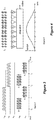
- Figure 1 shows a typical exemplary projected capacitive device with one or more receiver electrodes (rxi), and one or more optional stimuli nodes (txj).
- the transmitting lines tx n and the receiving lines rx n are arranged in a matrix such that the nodes where a transmission line crosses a receiving line form a capacitor that serves as the actual sensor.
- the matrix reduces the number of lines that would be otherwise needed.
- the example shown in Fig. 1 uses two receiving lines and four transmitting lines. However, any other number of lines may be used depending on the design.
- stimulus circuit TX such as, for example, I/O ports of a microcontroller, are connected to four emitting electrodes tx 0 , tx 1 , tx 2 , and tx 3 in this example.
- Figure 2 shows as an example bursts of stimuli pulses applied in a scan sequence to, for example, three emitting electrodes tx 0 , tx 1 , tx 2 and corresponding changes at times to, t 1 , t 2 ... of active emitting electrode tx0, tx 1 , tx 2 which delimit packets of samples. Note, that samples do not necessarily synchronize with stimuli pulses.
- the fourth transmission line is here not used for a better overview only. In figure 2 , one assumes each receiving electrode (rx0, rx1) has its own measurement circuit so measurements can be made in parallel.
- FIG. 3 shows such an alternative to figure 2 .
- the measure circuit is here multiplexed to different receiving electrodes, and packets of samples p 0 , p 1 , p 2 are delimited by changes of active receiving electrode rx 0 , rx 1 as well as active emitting electrodes tx 0 , tx 1 .
- Figure 4 shows a packet of samples acquired between a start and a stop time t i and ti+i, respectively.
- each sample is weighted by a gain a (a 0 , a 1..m , a e ).
- the resulting output is shown as the weighted sum.
- weight applied to samples near the transitions t i and ti+i get less importance in absolute value (a 0 , a e ) compared to samples in the middle of the packet (a m , a n ).
- a Gaussian weight curve may be applied.
- Other distribution weight curves may apply, such as Hamming, Hanning, Blackman etc., as long as the first and last measurements receive less gain than a center value.
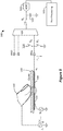
- Figure 5 shows an example of projected capacitive system with a single capacitive sensor 530, 540, for example, when touched by a finger 550 during the acquisition of one packet.
- sensor electrodes 530, 540 may be part of a matrix of electrodes.
- the capacitive sensor 530, 540 is coupled with an evaluation circuit comprising, for example, a multiplexer 505, sample and hold circuit S s , 510, an analog-to-digital converter 520 and a processing unit 570.
- multiplexer 505 is of course not needed unless the ADC 520 is used to sample other analog signals.
- the transmitting electrode 530 or a selected transmitting electrode from a matrix is connected to a source generating a stimulus tx and the receive electrode 540 or one of the receiving electrodes from a matrix is selected from which a signal rx is fed, for example, by an analog multiplexer 505 to a sample and hold circuit with switch S s and sample capacitor 510.
- the stimulus can be a series of pulses, wherein, for example, each pulse varies between ground and a supply voltage.
- a duty cycle of 50% may be used for a sequence of pulses. However, other duty cycles may apply.
- the pulses may be synchronized with the charging/discharging switches Sp, Sn as will be explained in more detail below.
- the sampled signal is then converted by an analog-to digital converter 520 into a digital value which is fed to a processing unit 570 for further processing.
- a finger 550 touches the cover material 560 above the electrodes 530, 540 and behaves also as a source of noise (Vnoise) which will influence the received voltage (Vrx).
- Vnoise source of noise
- the receiving electrode 540 can also be momentarily connected to Vdd or to Gnd by switches Sn, Sp to generate a pair of sample values as will be explained below in more detail.
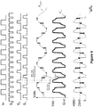
- Figure 6 shows a timing diagram of various signals of one embodiment which may for example use the arrangement shown in Fig. 5 .
- Fig. 6 shows one embodiment of a switching sequence and acquisition process.
- the receiving electrode 540 is momentarily connected to ground by switch Sn and signal Sn being high, while the sample and hold is tracking when signal Ss is high.
- a positive stimulus tx is applied on the emitting electrode 530, causing Vrx to rise.
- Vrx also changes -so long Sp or Sn switches are off- due to variation of the potential of the finger with respect to the ground.
- the sample and hold blocks the signal when signal Ss goes low, and a first or odd sample is acquired and converted. Then, while tx is still high and after the falling edge of Ss, switch Sp is closed for a short period by a positive pulse of signal Sp. Signal Ss then returns high, placing track and hold circuit again in tracking mode. Shortly thereafter, the stimulus tx returns to ground and thereafter, with the falling edge of Ss, a second or even sample is acquired. In this example values comprised between 0 and 4095. An arbitrary pivot value at 2048 is used to refer the amplitude of the samples. Fig. 6 shows that the signal acquired is alternately switched between ground and Vdd and altered from these starting points by the stimulus rx and the noise Vnoise.
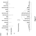
- Figure 7 shows the signals acquired according to the timing diagram of figure 6 after demodulation.
- the measurement samples are demodulated in this example by replacing the odd samples by new values equal to 2048-value, and the even samples by new values equal to +value-2048.
- This demodulation operation corrects the fact that the stimulus tx applied on transmitting electrode 530 alternates positive and negative edges.
- this figure illustrates how the samples near the beginning and end of the packet are mathematically multiplied by a smaller weight compared to samples in the middle of the packet as shown with the result after weighting in the bottom curve of Fig. 7 .
- the demodulation process is specific to the way of applying the stimulus tx. Other sampling schemes may apply. However, it shows that despite a change of the sign of some samples, their importance, or weight, still follows a gradually increasing and then decreasing importance.
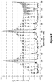
- Figure 8 shows an experimental comparison of noise level recorded without using the principles of the various embodiments (dashed stroke), and using the principles of the various embodiments (solid stroke). As can be seen the noise floor is significantly improved.
- Fig. 9 shows an example of a measurement sensor arrangement that can be used in a non-touching sensor application.
- a substrate 900 may comprise a transmitting electrode 920 and a plurality, here four, receiving electrodes 910a, b, c, d.
- Fig. 9 shows a frame-like support structure 900 that can be for example arranged around a display, keyboard, or trackpad, other shapes and forms for the substrate may apply.
- the transmitting electrode 920 may cover the entire backside of the substrate 900 and the receiving electrodes 910a, b, c, d may be arranged on the top side.
- Such an arrangement can be provided by a double sided printed circuit board wherein the electrodes are formed by the copper layers.
- a single-sided printed circuit board may also be used, wherein the transmitting electrode may simply surround the receiving electrodes. All electrodes may be coupled with a gesture detection controller 940 which detects predefined gestures and touches and generates commands that are fed to a main processing system 930.
- Fig. 10 shows another embodiment of a similar system 1000 combined with a touch pad 1020.
- the electrodes A, B, C, and D surround the touchpad 1020 which may be similar to the embodiment shown in Fig. 1 .
- the touchpad 1020 may be coupled with a touch controller 1010 whereas the electrodes A, B, C, D may be coupled with a 3D-gesture controller 1030.
- a transmission electrode (not shown) may be arranged below the sensor arrangement 1000 and coupled with the 3D-gesture controller 1030.
- the signals received from the various electrodes 910a, b, c, d of Fig. 9 or electrodes A, B, C, D of Fig. 10 may be received and converted in parallel or using a time-multiplexing scheme within the respective controller.
- the same various principles for evaluating sequential samples as discussed above also apply to these non-touching capacitive electrode sensor arrangements.
Landscapes
- Engineering & Computer Science (AREA)
- General Engineering & Computer Science (AREA)
- Theoretical Computer Science (AREA)
- Physics & Mathematics (AREA)
- General Physics & Mathematics (AREA)
- Human Computer Interaction (AREA)
- Power Engineering (AREA)
- Quality & Reliability (AREA)
- Position Input By Displaying (AREA)
- Electronic Switches (AREA)
- Measurement Of Resistance Or Impedance (AREA)
Applications Claiming Priority (3)
| Application Number | Priority Date | Filing Date | Title |
|---|---|---|---|
| US201562238318P | 2015-10-07 | 2015-10-07 | |
| US15/286,986 US10444892B2 (en) | 2015-10-07 | 2016-10-06 | Capacitance measurement device with reduced noise |
| PCT/US2016/055905 WO2017062717A1 (en) | 2015-10-07 | 2016-10-07 | Capacitance measurement device with reduced noise |
Publications (2)
| Publication Number | Publication Date |
|---|---|
| EP3360254A1 EP3360254A1 (en) | 2018-08-15 |
| EP3360254B1 true EP3360254B1 (en) | 2021-12-01 |
Family
ID=57206393
Family Applications (1)
| Application Number | Title | Priority Date | Filing Date |
|---|---|---|---|
| EP16787632.5A Active EP3360254B1 (en) | 2015-10-07 | 2016-10-07 | Capacitance measurement device with reduced noise |
Country Status (7)
Cited By (1)
| Publication number | Priority date | Publication date | Assignee | Title |
|---|---|---|---|---|
| EP3935481A4 (en) * | 2019-03-08 | 2022-12-28 | Chargepoint, Inc. | TOUCH SCREEN WITH ELECTRIC FIELD |
Families Citing this family (14)
| Publication number | Priority date | Publication date | Assignee | Title |
|---|---|---|---|---|
| US10108292B2 (en) * | 2015-04-22 | 2018-10-23 | Microchip Technology Incorporated | Capacitive sensor system with multiple transmit electrodes |
| US10444892B2 (en) * | 2015-10-07 | 2019-10-15 | Microchip Technology Incorporated | Capacitance measurement device with reduced noise |
| US10768746B1 (en) | 2016-05-10 | 2020-09-08 | Apple Inc. | Quasi-continuous-time sampling of discrete-time sampled signals |
| CN110199247B (zh) * | 2017-12-27 | 2022-07-29 | 深圳市汇顶科技股份有限公司 | 噪声检测方法及装置、电子设备和计算机可读存储介质 |
| US10901551B2 (en) * | 2018-03-01 | 2021-01-26 | Microchip Technology Incorporated | Method and system for touchless gesture detection and hover and touch detection |
| TWI774778B (zh) * | 2018-05-31 | 2022-08-21 | 李尚禮 | 應用於觸控辨識裝置之感測模組及其方法 |
| TWI774779B (zh) * | 2018-05-31 | 2022-08-21 | 李尚禮 | 應用於觸控辨識裝置之感測模組及其方法 |
| JP2020187427A (ja) * | 2019-05-10 | 2020-11-19 | 株式会社ジャパンディスプレイ | センサ装置 |
| DE102019209433A1 (de) * | 2019-06-28 | 2020-12-31 | Robert Bosch Gmbh | Sensoreinrichtung, insbesondere zur Erfassung von Objekten |
| US10790824B1 (en) * | 2019-07-03 | 2020-09-29 | Samsung Electro-Mechanics Co., Ltd. | Switching operation sensing apparatus with touch input member identification |
| KR102236099B1 (ko) * | 2019-10-25 | 2021-04-05 | 삼성전기주식회사 | 멀티 터치의 위치 식별이 가능한 터치 센싱 장치 및 전자 기기 |
| TWI779534B (zh) * | 2020-03-25 | 2022-10-01 | 昇佳電子股份有限公司 | 電容感測電路 |
| JP7423428B2 (ja) * | 2020-06-05 | 2024-01-29 | シャープ株式会社 | タッチパネル入力装置 |
| EP4386977A4 (en) * | 2021-10-24 | 2024-12-11 | Samsung Electronics Co., Ltd. | ELECTRONIC DEVICE AND METHOD FOR IDENTIFYING THE GRIP STATE OF AN ELECTRONIC DEVICE |
Family Cites Families (86)
| Publication number | Priority date | Publication date | Assignee | Title |
|---|---|---|---|---|
| CN1017746B (zh) * | 1988-05-31 | 1992-08-05 | 株式会社三丰 | 位置绝对测量用电容型测试装置 |
| JP2002501271A (ja) * | 1998-01-26 | 2002-01-15 | ウェスターマン,ウェイン | 手操作入力を統合する方法および装置 |
| US6297811B1 (en) * | 1999-06-02 | 2001-10-02 | Elo Touchsystems, Inc. | Projective capacitive touchscreen |
| US8279180B2 (en) * | 2006-05-02 | 2012-10-02 | Apple Inc. | Multipoint touch surface controller |
| CN102981678B (zh) * | 2006-06-09 | 2015-07-22 | 苹果公司 | 触摸屏液晶显示器 |
| TW200802058A (en) * | 2006-06-20 | 2008-01-01 | Egalax Inc | Scanning control device for capacitive touch panel |
| US9201556B2 (en) * | 2006-11-08 | 2015-12-01 | 3M Innovative Properties Company | Touch location sensing system and method employing sensor data fitting to a predefined curve |
| US8049732B2 (en) * | 2007-01-03 | 2011-11-01 | Apple Inc. | Front-end signal compensation |
| US8698727B2 (en) * | 2007-01-05 | 2014-04-15 | Apple Inc. | Backlight and ambient light sensor system |
| US7460441B2 (en) * | 2007-01-12 | 2008-12-02 | Microchip Technology Incorporated | Measuring a long time period |
| DE102007016408A1 (de) * | 2007-03-26 | 2008-10-02 | Ident Technology Ag | Mobiles Kommunikationsgerät und Eingabeeinrichtung hierfür |
| US8493331B2 (en) * | 2007-06-13 | 2013-07-23 | Apple Inc. | Touch detection using multiple simultaneous frequencies |
| US8035622B2 (en) * | 2008-03-27 | 2011-10-11 | Apple Inc. | SAR ADC with dynamic input scaling and offset adjustment |
| US7764213B2 (en) * | 2008-07-01 | 2010-07-27 | Microchip Technology Incorporated | Current-time digital-to-analog converter |
| WO2010004867A1 (ja) * | 2008-07-08 | 2010-01-14 | セイコーインスツル株式会社 | 静電検出装置、情報機器及び静電検出方法 |
| CN101673149B (zh) * | 2008-09-10 | 2011-11-23 | 太瀚科技股份有限公司 | 电磁手写输入装置及方法 |
| US20100261912A1 (en) * | 2009-02-17 | 2010-10-14 | Toshiyuki Toda | Bis-(1(2)h-tetrazol-5-yl)amine and production method therefor |
| US8659694B2 (en) * | 2009-12-31 | 2014-02-25 | Omnivision Technologies, Inc. | Pausing column readout in image sensors |
| KR101769889B1 (ko) * | 2010-02-10 | 2017-08-21 | 마이크로칩 테크놀로지 저머니 게엠베하 | 수동 입력 동작과 연관된 신호의 생성 시스템 및 방법 |
| DE102010007455B4 (de) * | 2010-02-10 | 2024-06-27 | Microchip Technology Germany Gmbh | System und Verfahren zum berührungslosen Erfassen und Erkennen von Gesten in einem dreidimensionalen Raum |
| JP5822403B2 (ja) * | 2010-02-26 | 2015-11-24 | シナプティクス インコーポレイテッド | 干渉を防止するための復調の変更 |
| CN102892922A (zh) * | 2010-03-17 | 2013-01-23 | 应用材料公司 | 用于远程等离子体源辅助的含硅膜沉积的方法和装置 |
| KR101001654B1 (ko) * | 2010-03-19 | 2010-12-15 | 주식회사 에임즈 | 터치 패널 구동 장치 및 터치 패널 구동 방법 |
| JP5429814B2 (ja) * | 2010-03-29 | 2014-02-26 | 株式会社ワコム | 指示体検出装置および検出センサ |
| US8542215B2 (en) * | 2010-04-30 | 2013-09-24 | Microchip Technology Incorporated | Mutual capacitance measurement in a multi-touch input device |
| US8933907B2 (en) * | 2010-04-30 | 2015-01-13 | Microchip Technology Incorporated | Capacitive touch system using both self and mutual capacitance |
| US20110291928A1 (en) * | 2010-05-31 | 2011-12-01 | Po-Ju Chou | Multifunctional flexible handwriting board and method for manufacturing the same |
| WO2012027003A1 (en) * | 2010-08-23 | 2012-03-01 | Cypress Semiconductor Corporation | Capacitance scanning proximity detection |
| US9389724B2 (en) * | 2010-09-09 | 2016-07-12 | 3M Innovative Properties Company | Touch sensitive device with stylus support |
| GB201021477D0 (en) * | 2010-12-17 | 2011-02-02 | Elliptic Laboratories As | Signal processing |
| CN103392162B (zh) * | 2011-02-25 | 2016-08-24 | 高通技术公司 | 电容式触摸感测构架 |
| US9086439B2 (en) * | 2011-02-25 | 2015-07-21 | Maxim Integrated Products, Inc. | Circuits, devices and methods having pipelined capacitance sensing |
| US8564565B2 (en) * | 2011-03-02 | 2013-10-22 | Perceptive Pixel Inc. | Reduction of noise in touch sensors |
| WO2012119638A1 (en) * | 2011-03-04 | 2012-09-13 | Telefonaktiebolaget L M Ericsson (Publ) | Sub-rack mounting bracket and assembly |
| US8729911B2 (en) * | 2011-04-19 | 2014-05-20 | Cypress Semiconductor Corporation | Usage of weighting matrices in multi-phase scanning modes |
| US8786295B2 (en) * | 2011-04-20 | 2014-07-22 | Cypress Semiconductor Corporation | Current sensing apparatus and method for a capacitance-sensing device |
| JP5885232B2 (ja) * | 2011-05-09 | 2016-03-15 | シナプティクス・ディスプレイ・デバイス合同会社 | タッチセンサパネルコントローラ及び半導体装置 |
| US9081450B1 (en) * | 2011-06-09 | 2015-07-14 | Maxim Integrated Products, Inc. | Identifying hover and/or palm input and rejecting spurious input for a touch panel |
| US20120313890A1 (en) * | 2011-06-09 | 2012-12-13 | Maxim Integrated Products, Inc. | Inter-symbol interfence reduction for touch panel systems |
| KR101304195B1 (ko) * | 2011-06-24 | 2013-09-05 | 주식회사 하이딥 | 향상된 노이즈 필터링 특성을 갖는 정전 용량 센서, 정전 용량 센서의 노이즈 필터링 방법 및 컴퓨터 판독 가능한 기록 매체 |
| DE102011078534B4 (de) * | 2011-07-01 | 2016-02-18 | Ident Technology Ag | Auswerteverfahren und Auswerteeinrichtung für einen kapazitiven Berührungssensor |
| US9071264B2 (en) * | 2011-10-06 | 2015-06-30 | Microchip Technology Incorporated | Microcontroller with sequencer driven analog-to-digital converter |
| CN102495701B (zh) * | 2011-11-16 | 2014-12-10 | 敦泰科技有限公司 | 一种电容触摸屏的触摸检测方法和触摸检测装置 |
| US9323379B2 (en) * | 2011-12-09 | 2016-04-26 | Microchip Technology Germany Gmbh | Electronic device with a user interface that has more than two degrees of freedom, the user interface comprising a touch-sensitive surface and contact-free detection means |
| GB2499242A (en) * | 2012-02-10 | 2013-08-14 | Alterix Ltd | methods of operating excitation circuitry and/or measurement circuitry in a digitiser and a method of manufacturing a transducer for a digitiser |
| US20130241887A1 (en) * | 2012-03-14 | 2013-09-19 | Texas Instruments Incorporated | Detecting and Tracking Touch on an Illuminated Surface |
| JP6225164B2 (ja) * | 2012-03-28 | 2017-11-01 | サーク・コーポレーション | 加重マスクを用いた単数および複数の指の抽出および位置計算 |
| US9791487B2 (en) * | 2012-03-29 | 2017-10-17 | Egalax_Empia Technology Inc. | Method and device for measuring signals |
| US9372582B2 (en) * | 2012-04-19 | 2016-06-21 | Atmel Corporation | Self-capacitance measurement |
| EP2667156B1 (en) * | 2012-05-25 | 2015-10-21 | Nxp B.V. | Capacitive position sensor system |
| JP5988295B2 (ja) * | 2012-08-08 | 2016-09-07 | アルプス電気株式会社 | 入力装置 |
| US9279874B2 (en) * | 2012-08-16 | 2016-03-08 | Microchip Technology Germany Gmbh | Signal processing for a capacitive sensor system with robustness to noise |
| US9568526B2 (en) * | 2012-09-13 | 2017-02-14 | Microchip Technology Incorporated | Noise detection and correction routines |
| US9128573B2 (en) * | 2012-09-14 | 2015-09-08 | STMicroelectronics S.r.l.; | High signal to noise ratio capacitive sensing analog front-end |
| US9389256B2 (en) * | 2012-09-14 | 2016-07-12 | Stmicroelectronics Asia Pacific Pte Ltd | High signal to noise ratio capacitive sensing analog front-end |
| US9098155B2 (en) * | 2012-10-12 | 2015-08-04 | Atmel Corporation | Self-capacitance measurement using compensation capacitor |
| US9268432B2 (en) * | 2012-10-19 | 2016-02-23 | Stmicroelectronics Asia Pacific Pte Ltd. | Touch panel having a master and slave controller and method for driving thereof |
| CN103593097B (zh) * | 2012-11-29 | 2017-03-01 | 敦泰科技有限公司 | 一种终端设备的触摸检测系统及终端设备 |
| KR102058437B1 (ko) * | 2013-02-25 | 2019-12-26 | 삼성전자주식회사 | 필터 값 추출기를 포함하는 터치 감지 장치 및 필터 값 추출기 |
| US8890841B2 (en) * | 2013-03-13 | 2014-11-18 | 3M Innovative Properties Company | Capacitive-based touch apparatus and method therefor, with reduced interference |
| US10352976B2 (en) * | 2013-03-15 | 2019-07-16 | Microchip Technology Incorporated | Matrix electrode design for three-dimensional e-filed sensor |
| US9007341B2 (en) * | 2013-06-25 | 2015-04-14 | Himax Technologies Limited | Touch system |
| US9001082B1 (en) * | 2013-09-27 | 2015-04-07 | Sensel, Inc. | Touch sensor detector system and method |
| US9665204B2 (en) * | 2013-10-04 | 2017-05-30 | Microchip Technology Incorporated | Continuous circle gesture detection for a sensor system |
| KR101580381B1 (ko) * | 2014-01-03 | 2015-12-28 | 삼성전기주식회사 | 터치 스크린 장치 및 그 제어 방법 |
| KR20150109042A (ko) * | 2014-03-19 | 2015-10-01 | 삼성전기주식회사 | 터치스크린 장치 및 터치 감지 방법 |
| US9256333B2 (en) * | 2014-04-15 | 2016-02-09 | Samsung Electronics Co., Ltd. | Method and apparatus for reducing noise in capacitive touch interfaces |
| US10459623B2 (en) * | 2014-04-17 | 2019-10-29 | Microchip Technology Incorporated | Touch detection in a capacitive sensor system |
| US10558302B2 (en) * | 2014-05-23 | 2020-02-11 | Apple Inc. | Coded integration of a self-capacitance array |
| JP6533536B2 (ja) * | 2014-06-26 | 2019-06-19 | マイクロチップ テクノロジー インコーポレイテッドMicrochip Technology Incorporated | 容量感知システム内のフィードラインへの標的物体の結合の補償 |
| US9927933B2 (en) * | 2014-07-10 | 2018-03-27 | Microchip Technology Germany Gmbh | Method and system for gesture detection and touch detection |
| EP2975501B1 (en) * | 2014-07-18 | 2023-08-02 | Semtech Corporation | A measuring circuit and measuring method for a capacitive touch-sensitive panel |
| US10649488B2 (en) * | 2014-08-20 | 2020-05-12 | Microchip Technology Germany Gmbh | Electrode arrangement for gesture detection and tracking |
| US9590649B2 (en) * | 2014-10-17 | 2017-03-07 | Microchip Technology Incorporated | Analog-to-digital conversion with micro-coded sequencer |
| US9542051B2 (en) * | 2014-10-24 | 2017-01-10 | Microchip Technology Incorporated | Analog elimination of ungrounded conductive objects in capacitive sensing |
| US9971442B2 (en) * | 2014-10-29 | 2018-05-15 | Microchip Technology Germany Gmbh | Human interface device and method |
| WO2016114267A1 (ja) * | 2015-01-13 | 2016-07-21 | 国立大学法人神戸大学 | オンチップモニタ回路及び半導体チップ |
| US10135424B2 (en) * | 2015-02-27 | 2018-11-20 | Microchip Technology Germany Gmbh | Digital filter with confidence input |
| US10277203B2 (en) * | 2015-02-27 | 2019-04-30 | Microchip Technology Germany Gmbh | Digital filter with confidence input |
| US10108292B2 (en) * | 2015-04-22 | 2018-10-23 | Microchip Technology Incorporated | Capacitive sensor system with multiple transmit electrodes |
| US10303285B2 (en) * | 2015-04-22 | 2019-05-28 | Microchip Technology Incorporated | Sensor device for a display |
| US9946397B2 (en) * | 2015-06-15 | 2018-04-17 | Microchip Technology Incorporated | Sensor design for enhanced touch and gesture decoding |
| US20170090609A1 (en) * | 2015-09-25 | 2017-03-30 | Synaptics Incorporated | Oversampled step and wait system for capacitive sensing |
| US10444892B2 (en) * | 2015-10-07 | 2019-10-15 | Microchip Technology Incorporated | Capacitance measurement device with reduced noise |
| US10151608B2 (en) * | 2015-12-22 | 2018-12-11 | Microchip Technology Incorporated | System and method for reducing noise in a sensor system |
| US10394332B2 (en) * | 2016-04-07 | 2019-08-27 | Microchip Technology Germany Gmbh | Sensor design for enhanced touch and gesture decoding |
-
2016
- 2016-10-06 US US15/286,986 patent/US10444892B2/en active Active
- 2016-10-07 EP EP16787632.5A patent/EP3360254B1/en active Active
- 2016-10-07 TW TW105132673A patent/TWI713604B/zh active
- 2016-10-07 JP JP2018513532A patent/JP2018536210A/ja active Pending
- 2016-10-07 KR KR1020187008694A patent/KR102558321B1/ko active Active
- 2016-10-07 WO PCT/US2016/055905 patent/WO2017062717A1/en active Application Filing
- 2016-10-07 CN CN201680057798.0A patent/CN108141212B/zh active Active
Non-Patent Citations (1)
| Title |
|---|
| None * |
Cited By (1)
| Publication number | Priority date | Publication date | Assignee | Title |
|---|---|---|---|---|
| EP3935481A4 (en) * | 2019-03-08 | 2022-12-28 | Chargepoint, Inc. | TOUCH SCREEN WITH ELECTRIC FIELD |
Also Published As
| Publication number | Publication date |
|---|---|
| JP2018536210A (ja) | 2018-12-06 |
| WO2017062717A1 (en) | 2017-04-13 |
| KR20180064397A (ko) | 2018-06-14 |
| TWI713604B (zh) | 2020-12-21 |
| CN108141212B (zh) | 2022-03-25 |
| TW201716788A (zh) | 2017-05-16 |
| US10444892B2 (en) | 2019-10-15 |
| KR102558321B1 (ko) | 2023-07-24 |
| CN108141212A (zh) | 2018-06-08 |
| EP3360254A1 (en) | 2018-08-15 |
| US20170102815A1 (en) | 2017-04-13 |
Similar Documents
| Publication | Publication Date | Title |
|---|---|---|
| EP3360254B1 (en) | Capacitance measurement device with reduced noise | |
| CN112236743B (zh) | 压力感测设备和方法 | |
| US11687192B2 (en) | Touch controller architecture | |
| KR102366237B1 (ko) | 제스처 검출 및 터치 검출을 위한 방법 및 시스템 | |
| KR101233435B1 (ko) | 멀티포인트 터치 표면 제어기 | |
| KR102325699B1 (ko) | 용량형 감지에서 비접지된 전도성 오브젝트들의 아날로그 제거 | |
| JP6894887B2 (ja) | センサシステム内に雑音を低減させるためのシステムおよび方法 | |
| US20120268142A1 (en) | Capacitive panel scanning with reduced number of sensing circuits | |
| WO2016006910A1 (ko) | 정전용량형 터치 패널 장치 및 구동방법 | |
| JP2013058045A (ja) | タッチパネルの容量検出回路、容量検出方法、およびそれを用いたタッチパネル入力装置、電子機器 | |
| CN111600590A (zh) | 电容检测电路和触控芯片 | |
| CN111902801B (zh) | 电容检测电路、触控芯片和电子设备 | |
| US20170293376A1 (en) | Hover sensor | |
| US20120113049A1 (en) | Sample and hold analog front end for a capacitive touchpad | |
| US20130234975A1 (en) | Capacitive touch system and method with auto-calibration | |
| Heo et al. | Highly improved SNR differential sensing method using parallel operation signaling for touch screen application | |
| CN117519518A (zh) | 电容检测电路及电子芯片、电子设备、显示装置 | |
| WO2016114123A1 (en) | A Capacitive Touch Panel with Matrix Electrode Pattern |
Legal Events
| Date | Code | Title | Description |
|---|---|---|---|
| STAA | Information on the status of an ep patent application or granted ep patent |
Free format text: STATUS: UNKNOWN |
|
| STAA | Information on the status of an ep patent application or granted ep patent |
Free format text: STATUS: THE INTERNATIONAL PUBLICATION HAS BEEN MADE |
|
| PUAI | Public reference made under article 153(3) epc to a published international application that has entered the european phase |
Free format text: ORIGINAL CODE: 0009012 |
|
| STAA | Information on the status of an ep patent application or granted ep patent |
Free format text: STATUS: REQUEST FOR EXAMINATION WAS MADE |
|
| 17P | Request for examination filed |
Effective date: 20180423 |
|
| AK | Designated contracting states |
Kind code of ref document: A1 Designated state(s): AL AT BE BG CH CY CZ DE DK EE ES FI FR GB GR HR HU IE IS IT LI LT LU LV MC MK MT NL NO PL PT RO RS SE SI SK SM TR |
|
| AX | Request for extension of the european patent |
Extension state: BA ME |
|
| DAV | Request for validation of the european patent (deleted) | ||
| DAX | Request for extension of the european patent (deleted) | ||
| STAA | Information on the status of an ep patent application or granted ep patent |
Free format text: STATUS: EXAMINATION IS IN PROGRESS |
|
| 17Q | First examination report despatched |
Effective date: 20200908 |
|
| GRAP | Despatch of communication of intention to grant a patent |
Free format text: ORIGINAL CODE: EPIDOSNIGR1 |
|
| STAA | Information on the status of an ep patent application or granted ep patent |
Free format text: STATUS: GRANT OF PATENT IS INTENDED |
|
| INTG | Intention to grant announced |
Effective date: 20210519 |
|
| GRAS | Grant fee paid |
Free format text: ORIGINAL CODE: EPIDOSNIGR3 |
|
| GRAA | (expected) grant |
Free format text: ORIGINAL CODE: 0009210 |
|
| STAA | Information on the status of an ep patent application or granted ep patent |
Free format text: STATUS: THE PATENT HAS BEEN GRANTED |
|
| AK | Designated contracting states |
Kind code of ref document: B1 Designated state(s): AL AT BE BG CH CY CZ DE DK EE ES FI FR GB GR HR HU IE IS IT LI LT LU LV MC MK MT NL NO PL PT RO RS SE SI SK SM TR |
|
| REG | Reference to a national code |
Ref country code: GB Ref legal event code: FG4D |
|
| REG | Reference to a national code |
Ref country code: AT Ref legal event code: REF Ref document number: 1452751 Country of ref document: AT Kind code of ref document: T Effective date: 20211215 Ref country code: CH Ref legal event code: EP |
|
| REG | Reference to a national code |
Ref country code: IE Ref legal event code: FG4D |
|
| REG | Reference to a national code |
Ref country code: DE Ref legal event code: R096 Ref document number: 602016066860 Country of ref document: DE |
|
| REG | Reference to a national code |
Ref country code: LT Ref legal event code: MG9D |
|
| REG | Reference to a national code |
Ref country code: NL Ref legal event code: MP Effective date: 20211201 |
|
| REG | Reference to a national code |
Ref country code: AT Ref legal event code: MK05 Ref document number: 1452751 Country of ref document: AT Kind code of ref document: T Effective date: 20211201 |
|
| PG25 | Lapsed in a contracting state [announced via postgrant information from national office to epo] |
Ref country code: RS Free format text: LAPSE BECAUSE OF FAILURE TO SUBMIT A TRANSLATION OF THE DESCRIPTION OR TO PAY THE FEE WITHIN THE PRESCRIBED TIME-LIMIT Effective date: 20211201 Ref country code: LT Free format text: LAPSE BECAUSE OF FAILURE TO SUBMIT A TRANSLATION OF THE DESCRIPTION OR TO PAY THE FEE WITHIN THE PRESCRIBED TIME-LIMIT Effective date: 20211201 Ref country code: FI Free format text: LAPSE BECAUSE OF FAILURE TO SUBMIT A TRANSLATION OF THE DESCRIPTION OR TO PAY THE FEE WITHIN THE PRESCRIBED TIME-LIMIT Effective date: 20211201 Ref country code: BG Free format text: LAPSE BECAUSE OF FAILURE TO SUBMIT A TRANSLATION OF THE DESCRIPTION OR TO PAY THE FEE WITHIN THE PRESCRIBED TIME-LIMIT Effective date: 20220301 Ref country code: AT Free format text: LAPSE BECAUSE OF FAILURE TO SUBMIT A TRANSLATION OF THE DESCRIPTION OR TO PAY THE FEE WITHIN THE PRESCRIBED TIME-LIMIT Effective date: 20211201 |
|
| PG25 | Lapsed in a contracting state [announced via postgrant information from national office to epo] |
Ref country code: SE Free format text: LAPSE BECAUSE OF FAILURE TO SUBMIT A TRANSLATION OF THE DESCRIPTION OR TO PAY THE FEE WITHIN THE PRESCRIBED TIME-LIMIT Effective date: 20211201 Ref country code: PL Free format text: LAPSE BECAUSE OF FAILURE TO SUBMIT A TRANSLATION OF THE DESCRIPTION OR TO PAY THE FEE WITHIN THE PRESCRIBED TIME-LIMIT Effective date: 20211201 Ref country code: NO Free format text: LAPSE BECAUSE OF FAILURE TO SUBMIT A TRANSLATION OF THE DESCRIPTION OR TO PAY THE FEE WITHIN THE PRESCRIBED TIME-LIMIT Effective date: 20220301 Ref country code: LV Free format text: LAPSE BECAUSE OF FAILURE TO SUBMIT A TRANSLATION OF THE DESCRIPTION OR TO PAY THE FEE WITHIN THE PRESCRIBED TIME-LIMIT Effective date: 20211201 Ref country code: HR Free format text: LAPSE BECAUSE OF FAILURE TO SUBMIT A TRANSLATION OF THE DESCRIPTION OR TO PAY THE FEE WITHIN THE PRESCRIBED TIME-LIMIT Effective date: 20211201 Ref country code: GR Free format text: LAPSE BECAUSE OF FAILURE TO SUBMIT A TRANSLATION OF THE DESCRIPTION OR TO PAY THE FEE WITHIN THE PRESCRIBED TIME-LIMIT Effective date: 20220302 Ref country code: ES Free format text: LAPSE BECAUSE OF FAILURE TO SUBMIT A TRANSLATION OF THE DESCRIPTION OR TO PAY THE FEE WITHIN THE PRESCRIBED TIME-LIMIT Effective date: 20211201 |
|
| PG25 | Lapsed in a contracting state [announced via postgrant information from national office to epo] |
Ref country code: NL Free format text: LAPSE BECAUSE OF FAILURE TO SUBMIT A TRANSLATION OF THE DESCRIPTION OR TO PAY THE FEE WITHIN THE PRESCRIBED TIME-LIMIT Effective date: 20211201 |
|
| PG25 | Lapsed in a contracting state [announced via postgrant information from national office to epo] |
Ref country code: SM Free format text: LAPSE BECAUSE OF FAILURE TO SUBMIT A TRANSLATION OF THE DESCRIPTION OR TO PAY THE FEE WITHIN THE PRESCRIBED TIME-LIMIT Effective date: 20211201 Ref country code: SK Free format text: LAPSE BECAUSE OF FAILURE TO SUBMIT A TRANSLATION OF THE DESCRIPTION OR TO PAY THE FEE WITHIN THE PRESCRIBED TIME-LIMIT Effective date: 20211201 Ref country code: RO Free format text: LAPSE BECAUSE OF FAILURE TO SUBMIT A TRANSLATION OF THE DESCRIPTION OR TO PAY THE FEE WITHIN THE PRESCRIBED TIME-LIMIT Effective date: 20211201 Ref country code: PT Free format text: LAPSE BECAUSE OF FAILURE TO SUBMIT A TRANSLATION OF THE DESCRIPTION OR TO PAY THE FEE WITHIN THE PRESCRIBED TIME-LIMIT Effective date: 20220401 Ref country code: EE Free format text: LAPSE BECAUSE OF FAILURE TO SUBMIT A TRANSLATION OF THE DESCRIPTION OR TO PAY THE FEE WITHIN THE PRESCRIBED TIME-LIMIT Effective date: 20211201 Ref country code: CZ Free format text: LAPSE BECAUSE OF FAILURE TO SUBMIT A TRANSLATION OF THE DESCRIPTION OR TO PAY THE FEE WITHIN THE PRESCRIBED TIME-LIMIT Effective date: 20211201 |
|
| REG | Reference to a national code |
Ref country code: DE Ref legal event code: R097 Ref document number: 602016066860 Country of ref document: DE |
|
| PG25 | Lapsed in a contracting state [announced via postgrant information from national office to epo] |
Ref country code: IS Free format text: LAPSE BECAUSE OF FAILURE TO SUBMIT A TRANSLATION OF THE DESCRIPTION OR TO PAY THE FEE WITHIN THE PRESCRIBED TIME-LIMIT Effective date: 20220401 |
|
| PLBE | No opposition filed within time limit |
Free format text: ORIGINAL CODE: 0009261 |
|
| STAA | Information on the status of an ep patent application or granted ep patent |
Free format text: STATUS: NO OPPOSITION FILED WITHIN TIME LIMIT |
|
| PG25 | Lapsed in a contracting state [announced via postgrant information from national office to epo] |
Ref country code: DK Free format text: LAPSE BECAUSE OF FAILURE TO SUBMIT A TRANSLATION OF THE DESCRIPTION OR TO PAY THE FEE WITHIN THE PRESCRIBED TIME-LIMIT Effective date: 20211201 Ref country code: AL Free format text: LAPSE BECAUSE OF FAILURE TO SUBMIT A TRANSLATION OF THE DESCRIPTION OR TO PAY THE FEE WITHIN THE PRESCRIBED TIME-LIMIT Effective date: 20211201 |
|
| 26N | No opposition filed |
Effective date: 20220902 |
|
| PG25 | Lapsed in a contracting state [announced via postgrant information from national office to epo] |
Ref country code: SI Free format text: LAPSE BECAUSE OF FAILURE TO SUBMIT A TRANSLATION OF THE DESCRIPTION OR TO PAY THE FEE WITHIN THE PRESCRIBED TIME-LIMIT Effective date: 20211201 |
|
| PG25 | Lapsed in a contracting state [announced via postgrant information from national office to epo] |
Ref country code: MC Free format text: LAPSE BECAUSE OF FAILURE TO SUBMIT A TRANSLATION OF THE DESCRIPTION OR TO PAY THE FEE WITHIN THE PRESCRIBED TIME-LIMIT Effective date: 20211201 Ref country code: IT Free format text: LAPSE BECAUSE OF FAILURE TO SUBMIT A TRANSLATION OF THE DESCRIPTION OR TO PAY THE FEE WITHIN THE PRESCRIBED TIME-LIMIT Effective date: 20211201 |
|
| REG | Reference to a national code |
Ref country code: CH Ref legal event code: PL |
|
| REG | Reference to a national code |
Ref country code: BE Ref legal event code: MM Effective date: 20221031 |
|
| GBPC | Gb: european patent ceased through non-payment of renewal fee |
Effective date: 20221007 |
|
| PG25 | Lapsed in a contracting state [announced via postgrant information from national office to epo] |
Ref country code: LU Free format text: LAPSE BECAUSE OF NON-PAYMENT OF DUE FEES Effective date: 20221007 |
|
| P01 | Opt-out of the competence of the unified patent court (upc) registered |
Effective date: 20230528 |
|
| PG25 | Lapsed in a contracting state [announced via postgrant information from national office to epo] |
Ref country code: LI Free format text: LAPSE BECAUSE OF NON-PAYMENT OF DUE FEES Effective date: 20221031 Ref country code: FR Free format text: LAPSE BECAUSE OF NON-PAYMENT OF DUE FEES Effective date: 20221031 Ref country code: CH Free format text: LAPSE BECAUSE OF NON-PAYMENT OF DUE FEES Effective date: 20221031 |
|
| PG25 | Lapsed in a contracting state [announced via postgrant information from national office to epo] |
Ref country code: BE Free format text: LAPSE BECAUSE OF NON-PAYMENT OF DUE FEES Effective date: 20221031 |
|
| PG25 | Lapsed in a contracting state [announced via postgrant information from national office to epo] |
Ref country code: IE Free format text: LAPSE BECAUSE OF NON-PAYMENT OF DUE FEES Effective date: 20221007 Ref country code: GB Free format text: LAPSE BECAUSE OF NON-PAYMENT OF DUE FEES Effective date: 20221007 |
|
| PG25 | Lapsed in a contracting state [announced via postgrant information from national office to epo] |
Ref country code: HU Free format text: LAPSE BECAUSE OF FAILURE TO SUBMIT A TRANSLATION OF THE DESCRIPTION OR TO PAY THE FEE WITHIN THE PRESCRIBED TIME-LIMIT; INVALID AB INITIO Effective date: 20161007 |
|
| PG25 | Lapsed in a contracting state [announced via postgrant information from national office to epo] |
Ref country code: CY Free format text: LAPSE BECAUSE OF FAILURE TO SUBMIT A TRANSLATION OF THE DESCRIPTION OR TO PAY THE FEE WITHIN THE PRESCRIBED TIME-LIMIT Effective date: 20211201 |
|
| PG25 | Lapsed in a contracting state [announced via postgrant information from national office to epo] |
Ref country code: MK Free format text: LAPSE BECAUSE OF FAILURE TO SUBMIT A TRANSLATION OF THE DESCRIPTION OR TO PAY THE FEE WITHIN THE PRESCRIBED TIME-LIMIT Effective date: 20211201 |
|
| PG25 | Lapsed in a contracting state [announced via postgrant information from national office to epo] |
Ref country code: TR Free format text: LAPSE BECAUSE OF FAILURE TO SUBMIT A TRANSLATION OF THE DESCRIPTION OR TO PAY THE FEE WITHIN THE PRESCRIBED TIME-LIMIT Effective date: 20211201 |
|
| PG25 | Lapsed in a contracting state [announced via postgrant information from national office to epo] |
Ref country code: MT Free format text: LAPSE BECAUSE OF FAILURE TO SUBMIT A TRANSLATION OF THE DESCRIPTION OR TO PAY THE FEE WITHIN THE PRESCRIBED TIME-LIMIT Effective date: 20211201 |
|
| PGFP | Annual fee paid to national office [announced via postgrant information from national office to epo] |
Ref country code: DE Payment date: 20240919 Year of fee payment: 9 |