EP3358828A1 - Bildaufnahmeelement und endoskop - Google Patents
Bildaufnahmeelement und endoskop Download PDFInfo
- Publication number
- EP3358828A1 EP3358828A1 EP16851453.7A EP16851453A EP3358828A1 EP 3358828 A1 EP3358828 A1 EP 3358828A1 EP 16851453 A EP16851453 A EP 16851453A EP 3358828 A1 EP3358828 A1 EP 3358828A1
- Authority
- EP
- European Patent Office
- Prior art keywords
- unit
- output
- transfer line
- pixel
- signal
- Prior art date
- Legal status (The legal status is an assumption and is not a legal conclusion. Google has not performed a legal analysis and makes no representation as to the accuracy of the status listed.)
- Withdrawn
Links
- 238000012546 transfer Methods 0.000 claims abstract description 312
- 238000003384 imaging method Methods 0.000 claims abstract description 288
- 238000006243 chemical reaction Methods 0.000 claims abstract description 85
- 238000012545 processing Methods 0.000 claims description 50
- 238000003780 insertion Methods 0.000 claims description 8
- 230000037431 insertion Effects 0.000 claims description 8
- 238000000411 transmission spectrum Methods 0.000 claims description 5
- 239000011159 matrix material Substances 0.000 claims description 4
- 238000005070 sampling Methods 0.000 description 97
- 238000010586 diagram Methods 0.000 description 16
- 230000005540 biological transmission Effects 0.000 description 13
- 239000003990 capacitor Substances 0.000 description 10
- 238000012986 modification Methods 0.000 description 10
- 230000004048 modification Effects 0.000 description 10
- 238000000034 method Methods 0.000 description 8
- 230000006870 function Effects 0.000 description 5
- 238000005286 illumination Methods 0.000 description 4
- 230000000694 effects Effects 0.000 description 2
- 238000005401 electroluminescence Methods 0.000 description 2
- 230000014509 gene expression Effects 0.000 description 2
- 239000002775 capsule Substances 0.000 description 1
- 230000000295 complement effect Effects 0.000 description 1
- 238000012937 correction Methods 0.000 description 1
- 238000013461 design Methods 0.000 description 1
- 238000009792 diffusion process Methods 0.000 description 1
- 238000001727 in vivo Methods 0.000 description 1
- 239000004973 liquid crystal related substance Substances 0.000 description 1
- 229910044991 metal oxide Inorganic materials 0.000 description 1
- 150000004706 metal oxides Chemical class 0.000 description 1
- 239000013307 optical fiber Substances 0.000 description 1
- 230000000644 propagated effect Effects 0.000 description 1
- 239000004065 semiconductor Substances 0.000 description 1
- 230000008054 signal transmission Effects 0.000 description 1
- 238000001228 spectrum Methods 0.000 description 1
- 230000000087 stabilizing effect Effects 0.000 description 1
Images


Classifications
-
- A—HUMAN NECESSITIES
- A61—MEDICAL OR VETERINARY SCIENCE; HYGIENE
- A61B—DIAGNOSIS; SURGERY; IDENTIFICATION
- A61B1/00—Instruments for performing medical examinations of the interior of cavities or tubes of the body by visual or photographical inspection, e.g. endoscopes; Illuminating arrangements therefor
- A61B1/04—Instruments for performing medical examinations of the interior of cavities or tubes of the body by visual or photographical inspection, e.g. endoscopes; Illuminating arrangements therefor combined with photographic or television appliances
- A61B1/05—Instruments for performing medical examinations of the interior of cavities or tubes of the body by visual or photographical inspection, e.g. endoscopes; Illuminating arrangements therefor combined with photographic or television appliances characterised by the image sensor, e.g. camera, being in the distal end portion
- A61B1/051—Details of CCD assembly
-
- A—HUMAN NECESSITIES
- A61—MEDICAL OR VETERINARY SCIENCE; HYGIENE
- A61B—DIAGNOSIS; SURGERY; IDENTIFICATION
- A61B1/00—Instruments for performing medical examinations of the interior of cavities or tubes of the body by visual or photographical inspection, e.g. endoscopes; Illuminating arrangements therefor
- A61B1/04—Instruments for performing medical examinations of the interior of cavities or tubes of the body by visual or photographical inspection, e.g. endoscopes; Illuminating arrangements therefor combined with photographic or television appliances
- A61B1/045—Control thereof
-
- G—PHYSICS
- G02—OPTICS
- G02B—OPTICAL ELEMENTS, SYSTEMS OR APPARATUS
- G02B23/00—Telescopes, e.g. binoculars; Periscopes; Instruments for viewing the inside of hollow bodies; Viewfinders; Optical aiming or sighting devices
- G02B23/24—Instruments or systems for viewing the inside of hollow bodies, e.g. fibrescopes
- G02B23/2476—Non-optical details, e.g. housings, mountings, supports
- G02B23/2484—Arrangements in relation to a camera or imaging device
-
- H—ELECTRICITY
- H04—ELECTRIC COMMUNICATION TECHNIQUE
- H04N—PICTORIAL COMMUNICATION, e.g. TELEVISION
- H04N23/00—Cameras or camera modules comprising electronic image sensors; Control thereof
- H04N23/10—Cameras or camera modules comprising electronic image sensors; Control thereof for generating image signals from different wavelengths
- H04N23/11—Cameras or camera modules comprising electronic image sensors; Control thereof for generating image signals from different wavelengths for generating image signals from visible and infrared light wavelengths
-
- H—ELECTRICITY
- H04—ELECTRIC COMMUNICATION TECHNIQUE
- H04N—PICTORIAL COMMUNICATION, e.g. TELEVISION
- H04N23/00—Cameras or camera modules comprising electronic image sensors; Control thereof
- H04N23/50—Constructional details
- H04N23/555—Constructional details for picking-up images in sites, inaccessible due to their dimensions or hazardous conditions, e.g. endoscopes or borescopes
-
- H—ELECTRICITY
- H04—ELECTRIC COMMUNICATION TECHNIQUE
- H04N—PICTORIAL COMMUNICATION, e.g. TELEVISION
- H04N25/00—Circuitry of solid-state image sensors [SSIS]; Control thereof
- H04N25/70—SSIS architectures; Circuits associated therewith
- H04N25/76—Addressed sensors, e.g. MOS or CMOS sensors
-
- H—ELECTRICITY
- H04—ELECTRIC COMMUNICATION TECHNIQUE
- H04N—PICTORIAL COMMUNICATION, e.g. TELEVISION
- H04N25/00—Circuitry of solid-state image sensors [SSIS]; Control thereof
- H04N25/70—SSIS architectures; Circuits associated therewith
- H04N25/76—Addressed sensors, e.g. MOS or CMOS sensors
- H04N25/766—Addressed sensors, e.g. MOS or CMOS sensors comprising control or output lines used for a plurality of functions, e.g. for pixel output, driving, reset or power
-
- H—ELECTRICITY
- H04—ELECTRIC COMMUNICATION TECHNIQUE
- H04N—PICTORIAL COMMUNICATION, e.g. TELEVISION
- H04N25/00—Circuitry of solid-state image sensors [SSIS]; Control thereof
- H04N25/70—SSIS architectures; Circuits associated therewith
- H04N25/76—Addressed sensors, e.g. MOS or CMOS sensors
- H04N25/767—Horizontal readout lines, multiplexers or registers
-
- H—ELECTRICITY
- H04—ELECTRIC COMMUNICATION TECHNIQUE
- H04N—PICTORIAL COMMUNICATION, e.g. TELEVISION
- H04N25/00—Circuitry of solid-state image sensors [SSIS]; Control thereof
- H04N25/70—SSIS architectures; Circuits associated therewith
- H04N25/76—Addressed sensors, e.g. MOS or CMOS sensors
- H04N25/77—Pixel circuitry, e.g. memories, A/D converters, pixel amplifiers, shared circuits or shared components
- H04N25/778—Pixel circuitry, e.g. memories, A/D converters, pixel amplifiers, shared circuits or shared components comprising amplifiers shared between a plurality of pixels, i.e. at least one part of the amplifier must be on the sensor array itself
-
- H—ELECTRICITY
- H04—ELECTRIC COMMUNICATION TECHNIQUE
- H04N—PICTORIAL COMMUNICATION, e.g. TELEVISION
- H04N25/00—Circuitry of solid-state image sensors [SSIS]; Control thereof
- H04N25/70—SSIS architectures; Circuits associated therewith
- H04N25/76—Addressed sensors, e.g. MOS or CMOS sensors
- H04N25/779—Circuitry for scanning or addressing the pixel array
-
- H—ELECTRICITY
- H04—ELECTRIC COMMUNICATION TECHNIQUE
- H04N—PICTORIAL COMMUNICATION, e.g. TELEVISION
- H04N25/00—Circuitry of solid-state image sensors [SSIS]; Control thereof
- H04N25/70—SSIS architectures; Circuits associated therewith
- H04N25/76—Addressed sensors, e.g. MOS or CMOS sensors
- H04N25/78—Readout circuits for addressed sensors, e.g. output amplifiers or A/D converters
-
- A—HUMAN NECESSITIES
- A61—MEDICAL OR VETERINARY SCIENCE; HYGIENE
- A61B—DIAGNOSIS; SURGERY; IDENTIFICATION
- A61B1/00—Instruments for performing medical examinations of the interior of cavities or tubes of the body by visual or photographical inspection, e.g. endoscopes; Illuminating arrangements therefor
- A61B1/00163—Optical arrangements
- A61B1/00186—Optical arrangements with imaging filters
-
- A—HUMAN NECESSITIES
- A61—MEDICAL OR VETERINARY SCIENCE; HYGIENE
- A61B—DIAGNOSIS; SURGERY; IDENTIFICATION
- A61B1/00—Instruments for performing medical examinations of the interior of cavities or tubes of the body by visual or photographical inspection, e.g. endoscopes; Illuminating arrangements therefor
- A61B1/06—Instruments for performing medical examinations of the interior of cavities or tubes of the body by visual or photographical inspection, e.g. endoscopes; Illuminating arrangements therefor with illuminating arrangements
- A61B1/0661—Endoscope light sources
- A61B1/0676—Endoscope light sources at distal tip of an endoscope
-
- H—ELECTRICITY
- H04—ELECTRIC COMMUNICATION TECHNIQUE
- H04N—PICTORIAL COMMUNICATION, e.g. TELEVISION
- H04N23/00—Cameras or camera modules comprising electronic image sensors; Control thereof
- H04N23/10—Cameras or camera modules comprising electronic image sensors; Control thereof for generating image signals from different wavelengths
- H04N23/12—Cameras or camera modules comprising electronic image sensors; Control thereof for generating image signals from different wavelengths with one sensor only
Definitions
- the present invention relates to an image sensor and an endoscope for capturing images of a subject to generate image data of the subject.
- CMOS complementary metal oxide semiconductor
- Patent Literature 1 Japanese Patent No. 5596888
- the present invention has been made in view of the foregoing, and an object of the invention is to provide an image sensor capable of avoiding the variation in the image signals from pixels having filters of the same color arranged on the light receiving surface.
- an image sensor includes: a light receiving unit including: a plurality of unit pixels arranged in a two-dimensional matrix form, each of the plurality of unit pixels having a plurality of photoelectric converters for converting received light into imaging signals and outputting the imaging signals; and filters having different transmission spectra and disposed on light receiving surfaces of the plurality of photoelectric converters adjacent in a row direction; a plurality of first transfer lines each sharing a predetermined number of pixels in the row direction and configured to transfer the imaging signals; a constant current source provided for each of the plurality of first transfer lines and configured to transfer the imaging signals output from the plurality of unit pixels to each of the plurality of first transfer lines; a plurality of sample-and-hold units provided for the plurality of first transfer lines and configured to sample the imaging signals; a plurality of second transfer line configured to transfer the imaging signals sampled by the plurality of sample-and-hold units; a plurality of signal processing units provided corresponding to the number of the pluralit
- control unit is configured to cause the switching unit to switch the transfer destination of the imaging signals transferred from the plurality of second transfer lines so as to transfer the imaging signals output from the plurality of photoelectric converters having the light receiving surfaces on which the filters of a same type are disposed, to a same signal processing unit of the plurality of signal processing units.
- each of the plurality of unit pixels includes: a charge voltage converter; a plurality of charge transfer units configured to transfer charges from the plurality of photoelectric converters to the charge voltage converter; and an output unit configured to output the imaging signals after voltage conversion by the charge voltage converter.
- the number of the plurality of charge transfer units in each row of the plurality of unit pixels is two. Eeach of the two charge transfer units is connected to a first signal line or a second signal line to input a command signal for outputting the imaging signals at different points in time.
- the number of the multiple pixel units is two.
- a type of one of the filters disposed on one of the plurality of photoelectric converters to output the imaging signals from a first one of the two charge transfer units connected to the first signal line in a first one of the two pixel units is different from a type of another one of the filters disposed on another one of the plurality of photoelectric converters to output the imaging signals from the first one of the two charge transfer units connected to the first signal line in a second one of the two pixel units.
- a type of one of the filters disposed on one of the plurality of photoelectric converters to output the imaging signals from a second one of the two charge transfer units connected to the second signal line in the first one of the two pixel units is different from a type of another one of the filters disposed on another one of the plurality of photoelectric converters to output the imaging signals from the second one of the two charge transfer units connected to the second signal line in the second one of the two pixel units.
- each of the filters disposed on the light receiving surfaces of the plurality of photoelectric converters is one of a red filter, a green filter, and a blue filter.
- the number of the plurality of signal processing units is two.
- One of the two signal processing units is configured to perform the signal processing only on the imaging signals output from a photoelectric converter on which the green filter is disposed, among the plurality of photoelectric converters.
- An endoscope according to the invention includes the image sensor on a distal end of an insertion portion configured to be inserted into a subject.
- an endoscope system including an endoscope in which an image sensor is provided at a distal end of an insertion portion configured to be inserted into a subject.
- the present invention is not limited by the embodiments.
- the same reference signs are used to designate the same elements throughout the drawings.
- the drawings are schematic, the relationship between the thickness and the width of each member, the ratio of each member, etc. are different from the reality. Differences between dimensions and ratios of each other are also included in the drawings.
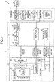
- FIG. 1 is a schematic diagram schematically illustrating the overall configuration of an endoscope system according to a first embodiment of the present invention.
- An endoscope system 1 illustrated in FIG. 1 includes an endoscope 2, a transmission cable 3, a connector unit 5, a processor 6 (processing device), a display device 7, and a light source device 8.
- the endoscope 2 images the inside of the body of the subject by inserting an insertion portion 100 which is a part of the transmission cable 3 into a body cavity of the subject, and outputs the imaging signal (image data) to the processor 6. Further, the endoscope 2 is one end of the transmission cable 3, an imaging unit 20 (imaging device) that images an in-vivo image is provided on a distal end 101 side of the insertion portion 100 to be inserted into the body cavity of the subject. An operating unit 4 for receiving various operations on the endoscope 2 is provided on a proximal end 102 side of the insertion portion 100.
- the imaging signal of the image imaged by the imaging unit 20 passes through the transmission cable 3 having a length of several meters, for example, and is output to the connector unit 5.
- the transmission cable 3 connects the endoscope 2 and the connector unit 5 and connects the endoscope 2 and the light source device 8. Further, the transmission cable 3 propagates the imaging signal generated by the imaging unit 20 to the connector unit 5.
- the transmission cable 3 is configured using a cable, an optical fiber, or the like.
- the connector unit 5 is connected to the endoscope 2, the processor 6, and the light source device 8, performs predetermined signal processing on imaging signals outputted from the connected endoscope 2, and converts an analog imaging signal into a digital imaging signal (A/D conversion) and outputs the digital imaging signal to the processor 6.
- the processor 6 is configured to perform predetermined image processing on an imaging signal input from the connector unit 5 and outputs the imaging signal to the display device 7.
- the processor 6 is configured to perform overall control of the endoscope system 1.
- the processor 6 is configured to switch the illumination light emitted from the light source device 8 and to switch between the imaging modes of the endoscope 2.
- the display device 7 is configured to display images corresponding to the imaging signal after the image processing by the processor 6. Further, the display device 7 displays various kinds of information on the endoscope system 1.
- the display device 7 is configured using a display panel such as liquid crystal or organic EL (Electro Luminescence) or the like.
- the light source device 8 is configured to irradiate the subject with the illumination light from the distal end 101 of the insertion portion 100 of the endoscope 2 via the connector unit 5 and the transmission cable 3.
- the light source device 8 includes a white light emitting diode (LED) for emitting white light and an LED for emitting special light of narrow band light having a narrower wavelength band than a wavelength band of white light.
- LED white light emitting diode
- the light source device 8 is configured to irradiate the subject with white light or narrow band light via the endoscope 2.
- FIG. 2 is a block diagram illustrating functions of a main part of the endoscope system 1. With reference to FIG. 2 , the details of each part configuration of the endoscope system 1 and the path of the electric signal in the endoscope system 1 will be described.
- the endoscope 2 illustrated in FIG. 2 includes the imaging unit 20, the transmission cable 3, and the connector unit 5.
- the imaging unit 20 includes a first chip 21 (image sensor) and a second chip 22.
- the imaging unit 20 receives the power supply voltage VDD generated by a power supply voltage generator 55 of the connector unit 5 described below via the transmission cable 3, together with the ground GND.
- a power supply stabilizing capacitor C1 is provided between the power supply voltage VDD supplied to the imaging unit 20 and the ground GND.
- the first chip 21 includes a light receiving unit 23 which is arranged in a two-dimensional matrix and has a plurality of unit pixels 230 which receive light from the outside and generate and output an image signal corresponding to the amount of received light, a reading unit 24 that reads out the imaging signal photoelectrically converted by each of the plurality of unit pixels 230 in the light receiving unit 23, a timing generator 25 that generates a timing signal based on a reference clock signal and a synchronization signal input from the connector unit 5 and outputs the timing signal to the reading unit 24, and a color filter 26 disposed on each light receiving surface of the plurality of unit pixels 230.
- a light receiving unit 23 which is arranged in a two-dimensional matrix and has a plurality of unit pixels 230 which receive light from the outside and generate and output an image signal corresponding to the amount of received light
- a reading unit 24 that reads out the imaging signal photoelectrically converted by each of the plurality of unit pixels 230 in the light receiving unit 23, a timing generator 25 that generates a timing signal
- the color filter 26 is realized by using a color filter of Bayer array configured by a red filter (hereinafter referred to as "R filter”) having a maximum value of a transmission spectrum in a red wavelength band, a green filter (hereinafter referred to as “G filter”) having a maximum value of a transmission spectrum in a green wavelength band, and a blue filter (hereinafter referred to as "B filter”) having a maximum value of a transmission spectrum in a blue wavelength band.
- R filter red filter
- G filter green filter
- B filter blue filter
- the R filter and the G filter are alternately arranged in this order in the odd-numbered rows of the light receiving unit 23, and the G filter and the B filter are alternately arranged in this order in the even-numbered rows of the light receiving unit 23.
- a photoelectric conversion element having a light receiving surface on which the R filter is disposed is referred to as a R pixel
- a photoelectric conversion element on which the G filter is disposed is referred to as a G pixel
- a photoelectric conversion element on which the B filter is disposed is referred to as a B pixel.
- the second chip 22 has a buffer 27 for amplifying an imaging signal output from each of the plurality of unit pixels 230 in the first chip 21 and outputting the imaging signal to the transmission cable 3.
- the combination of circuits arranged in the first chip 21 and the second chip 22 can be appropriately changed.
- the timing generator 25 arranged in the first chip 21 may be arranged in the second chip 22.
- the connector unit 5 includes an analog front end unit 51 (hereinafter referred to as "AFE unit 51"), an A/D converter 52, an imaging signal processing unit 53, a drive pulse generator 54, and a power supply voltage generator 55.
- the AFE unit 51 receives the imaging signal propagated from the imaging unit 20, performs impedance matching using a passive element such as a resistor, takes out an AC component by using a capacitor, and determines an operating point by a voltage dividing resistor. Thereafter, the AFE unit 51 corrects the imaging signal (analog signal) and outputs the imaging signal to the A/D converter 52.
- the A/D converter 52 converts the analog imaging signal input from the AFE unit 51 into a digital imaging signal and outputs the digital imaging signal to the imaging signal processing unit 53.
- the imaging signal processing unit 53 is constituted by, for example, a Field Programmable Gate Array (FPGA), performs processing such as noise removal and format conversion processing on the digital imaging signal input from the A/D converter 52, and outputs the resultant signal to the processor 6.
- FPGA Field Programmable Gate Array
- the drive pulse generator 54 Based on a reference clock signal (for example, a clock signal of 27 MHz) that is supplied from the processor 6 and serves as a reference of the operation of each element of the endoscope 2, the drive pulse generator 54 generates a synchronization signal indicating the start position of each frame and outputs the synchronization signal together with the reference clock signal to the timing generator 25 of the imaging unit 20 via the transmission cable 3.
- the synchronization signal generated by the drive pulse generator 54 includes a horizontal synchronization signal and a vertical synchronization signal.
- the power supply voltage generator 55 generates a power supply voltage necessary for driving the first chip 21 and the second chip 22 from the power supplied from the processor 6 and outputs the power supply voltage to the first chip 21 and the second chip 22.
- the power supply voltage generator 55 generates a power supply voltage necessary for driving the first chip 21 and the second chip 22 by using a regulator or the like.
- the processor 6 is a control device that totally controls the entire endoscope system 1.
- the processor 6 includes a power supply unit 61, an image signal processing unit 62, a clock generator 63, a recording unit 64, an input unit 65, and a processor controller 66.
- the power supply unit 61 generates the power supply voltage VDD and supplies the generated power supply voltage VDD to the power supply voltage generator 55 of the connector unit 5 together with the ground (GND).
- the image signal processing unit 62 performs, on the digital imaging signal subjected to the signal processing by the imaging signal processing unit 53, image processing such as a synchronization process, a white balance (WB) adjustment process, a gain adjustment process, a gamma correction process, a digital analog (D/A) conversion process, a format conversion process, and converts the digital imaging signal into an image signal, and outputs the image signal to the display device 7.
- image processing such as a synchronization process, a white balance (WB) adjustment process, a gain adjustment process, a gamma correction process, a digital analog (D/A) conversion process, a format conversion process, and converts the digital imaging signal into an image signal, and outputs the image signal to the display device 7.
- the clock generator 63 generates a reference clock signal which serves as a reference for the operation of each element of the endoscope system 1 and outputs the reference clock signal to the drive pulse generator 54.
- the recording unit 64 records various kinds of information on the endoscope system 1, data under processing, and the like.
- the recording unit 64 is configured by using a recording medium of a flash memory or a RAM (Random Access Memory).
- the input unit 65 receives inputs of various operations related to the endoscope system 1. For example, the input unit 65 receives input of a command signal for switching the type of illumination light emitted from the light source device 8.
- the input unit 65 is configured using, for example, a cross switch, a push button, or the like.
- the processor controller 66 totally controls each unit constituting the endoscope system 1.
- the processor controller 66 is configured using a CPU (Central Processing Unit) or the like.
- the processor controller 66 switches the illumination light emitted from the light source device 8 in accordance with the command signal input from the input unit 65.
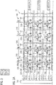
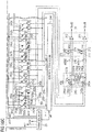
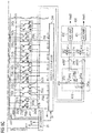
- FIG. 3 is a circuit diagram illustrating a configuration of the first chip 21 illustrated in FIG. 2 .
- a coordinate of the photoelectric conversion element in which the R filter, the G filter, and the B filter are arranged is expressed as Rxy.
- Rxy a coordinate of the photoelectric conversion element in which the R filter is arranged.
- one row and one column of the photoelectric conversion element in which the R filter is arranged is R11
- one row and two columns of the photoelectric conversion element in which the G filter is arranged are expressed as G12.
- the first chip 21 includes a timing generator 25, an output unit 31, a constant current source 240, a vertical scanning unit 241 (row selection circuit), a first sample-and-hold unit 242, a second sample-and-hold unit 243, a horizontal scanning unit 244 (column selecting circuit), a switching unit 245, and a horizontal reset unit 246.
- the timing generator 25 Based on the reference clock signal and the synchronization signal, the timing generator 25 generates various drive pulses (V control signals, ⁇ hclr, ⁇ NS, ⁇ SS, ⁇ H and ⁇ SW), and outputs the various drive pulses to the vertical scanning unit 241, the first sample-and-hold unit 242, the second sample-and-hold unit 243, the horizontal scanning unit 244, the switching unit 245, and the horizontal reset unit 246 which will be described later.
- the timing generator 25 functions as a control unit.
- the timing generator 25 causes the switching unit 245 to switch the transfer destination of the imaging signal transferred from a second horizontal transfer line 260 and a fourth horizontal transfer line 262 to either a first output amplifier unit 311 or a second output amplifier unit 312, and in the case of outputting the imaging signal from the unit pixel 230 for one row to the plurality of sample-and-hold units from the plurality of pixel units G1 and G2, controls the vertical scanning unit 241 so as to output the imaging signal in a predetermined number of times during one horizontal scanning period, divide the unit pixel 230 into a plurality of pixel units at each time of output, and output the imaging signal from the photoelectric conversion element in which different kinds of filters are arranged on the light receiving surface from each pixel unit.
- the constant current source 240 is connected to the ground GND, the other end is connected to a vertical transfer line 239, and a signal line to which the reference voltage Vbias is input is connected to the gate.
- the constant current source 240 is provided in each vertical transfer line 239 (first transfer line).
- V control signals ( ⁇ X, ⁇ R, ⁇ T1, ⁇ T2, etc.)
- each of a row selection pulse ⁇ X ⁇ M> , a drive pulse ⁇ R ⁇ M> , a drive pulse ⁇ T1 ⁇ M> and a drive pulse ⁇ T2 ⁇ M> by driving each unit pixel 230 of the light receiving unit 23 with the constant current source 240 connected to the vertical transfer line 239, the vertical scanning unit 241 transfers the imaging signal and the noise signal at the time of pixel reset by the vertical transfer line 239, and outputs each of the noise signal and the imaging signal to the first sample-and-hold unit 242 or the second sample-and-hold unit 243.
- the vertical scanning unit 241 transfers the imaging signal and the noise signal at the time of pixel reset by the vertical transfer line 239, and outputs each of the noise signal and the imaging signal to the first sample-and-hold unit 242 or the second sample-and-hold unit 243.
- the first sample-and-hold unit 242 samples the noise signal at the time of pixel reset in each unit pixel 230 which outputs the imaging signal via the vertical transfer line 239 of the odd number column, and outputs the sampled noise signal to the output unit 31. Furthermore, the first sample-and-hold unit 242 samples the imaging signal photoelectrically converted by each unit pixel 230 that outputs the imaging signal via the vertical transfer line 239 of the odd number column and outputs the sampled imaging signal to the output unit 31.
- the first sample-and-hold unit 242 includes a first sampling switch 251, a first sampling unit 252 (capacitor), a first output switch 253, a second sampling switch 254, a second sampling unit 255, and a second output switch 256.
- the first sampling switch 251 has one end connected to the vertical transfer line 239 of odd number column, the other end connected to one end of the first output switch 253, and a gate connected to a signal line into which a drive pulse ⁇ NS is input from the timing generator 25.
- the first sampling unit 252 has one end connected between the first sampling switch 251 and the first output switch 253, and the other end connected to the ground GND.
- the first sampling unit 252 samples (holds) the noise signal from the unit pixel 230.
- the first output switch 253 has one end connected to the first sampling switch 251, the other end connected to a first horizontal transfer line 259, and a gate into which a column selection pulse ⁇ H ⁇ M> is input from the horizontal scanning unit 244.
- the first output switch 253 transfers the noise signal sampled by the first sampling unit 252 to the first horizontal transfer line 259.
- the second sampling switch 254 has one end connected to the vertical transfer line 239, the other end connected to one end of the second output switch 256, and a gate connected to a signal line into which a drive pulse ⁇ SS is input from the timing generator 25.
- the second sampling unit 255 has one end connected between the second sampling switch 254 and the second output switch 256, and the other end connected to the ground GND.
- the second sampling unit 255 samples (holds) the imaging signal from the unit pixel 230.
- the second output switch 256 has one end connected to the second sampling switch 254, the other end connected to a second horizontal transfer line 260, and a gate into which the column selection pulse ⁇ H ⁇ M> is input from the horizontal scanning unit 244.
- the second output switch 256 transfers the imaging signal sampled by the second sampling unit 255 to the second horizontal transfer line 260.
- the second sample-and-hold unit 243 (sample-and-hold circuit) has the same configuration as the first sample-and-hold unit 242, samples the noise signal at the time of pixel reset in each unit pixel 230 which outputs the imaging signal via the vertical transfer line 239 of the even number column, and outputs the sampled noise signal to the output unit 31. Furthermore, the second sample-and-hold unit 243 samples the imaging signal photoelectrically converted by each unit pixel 230 that outputs the imaging signal via the vertical transfer line 239 of the even number column and outputs the sampled imaging signal to the output unit 31.
- the second sample-and-hold unit 243 includes a first sampling switch 251a, a first sampling unit 252a (capacitor), a first output switch 253a, a second sampling switch 254a, a second sampling unit 255a, and a second output switch 256a.
- the first sampling switch 251a has one end connected to the vertical transfer line 239 of even number column, the other end connected to one end of the first output switch 253a, and a gate connected to a signal line into which a drive pulse ⁇ NS is input from the timing generator 25.
- the first sampling unit 252a has one end connected between the first sampling switch 251a and the first output switch 253a, and the other end connected to the ground GND.
- the first sampling unit 252a samples (holds) the noise signal from the unit pixel 230.
- the first output switch 253a has one end connected to the first sampling switch 251a, the other end connected to a third horizontal transfer line 261, and a gate into which the column selection pulse ⁇ H ⁇ M> is input from the horizontal scanning unit 244.
- the first output switch 253a transfers the noise signal sampled by the first sampling unit 252a to the third horizontal transfer line 261.
- the second sampling switch 254a has one end connected to the vertical transfer line 239, the other end connected to one end of the second output switch 256a, and a gate connected to a signal line into which a drive pulse ⁇ SS is input from the timing generator 25.
- the second sampling unit 255a has one end connected between the second sampling switch 254a and the second output switch 256a, and the other end connected to the ground GND.
- the second sampling unit 255a samples (holds) the imaging signal from the unit pixel 230.
- the second output switch 256a has one end connected to the second sampling switch 254a, the other end connected to a fourth horizontal transfer line 262, and a gate into which the column selection pulse ⁇ H ⁇ M> is input from the horizontal scanning unit 244.
- the second output switch 256a transfers the imaging signal sampled by the second sampling unit 255a to the fourth horizontal transfer line 262.
- M 1, 2, 3, ..., m
- the horizontal scanning unit 244 applies the column selection pulse ⁇ H ⁇ M> to the selected row ⁇ M> of the light receiving unit 23, transfers the imaging signal photoelectrically converted by each unit pixel 230 to the second horizontal transfer line 260 via the first sample-and-hold unit 242 and output the noise signal, transfers the noise signal to the fourth horizontal transfer line 262 via the second sample-and-hold unit 243 and outputs the noise signal.
- the vertical scanning unit 241 and the horizontal scanning unit 244 function as the reading unit 24.
- the switching unit 245 connects the first horizontal transfer line 259, the second horizontal transfer line 260, the third horizontal transfer line 261, and the fourth horizontal transfer line 262 to any one of the first output amplifier unit 311 and the second output amplifier unit 312 of the output unit 31 to be described later.
- the switching unit 245 includes a first selection switch 245a, a second selection switch 245b, a third selection switch 245c, a fourth selection switch 245d, a fifth selection switch 245e, a sixth selection switch 245f, a seventh selection switch 245g, an eighth selection switch 245h, and an inversion element 270.
- the first selection switch 245a has one end connected to the first horizontal transfer line 259, the other end side connected to the first output amplifier unit 311 of the output unit 31 to be described later, and a gate connected to a signal line into which a drive pulse ⁇ SW is applied from the timing generator 25.
- the first selection switch 245a connects the first horizontal transfer line 259 and the first output amplifier unit 311 when the drive pulse ⁇ SW is applied to the gate.
- the second selection switch 245b has one end connected to the second horizontal transfer line 260, the other end side connected to the first output amplifier unit 311 of the output unit 31 to be described later, and a gate connected to a signal line into which a drive pulse ⁇ SW is applied from the timing generator 25.
- the second selection switch 245b connects the second horizontal transfer line 260 and the first output amplifier unit 311 when the drive pulse ⁇ SW is applied to the gate.
- the third selection switch 245c has one end connected to the third horizontal transfer line 261, the other end side connected to the second output amplifier unit 312 of the output unit 31 to be described later, and a gate connected to a signal line into which a drive pulse ⁇ SW is applied from the timing generator 25.
- the third selection switch 245c connects the third horizontal transfer line 261 and the second output amplifier unit 312 when the drive pulse ⁇ SW is applied to the gate.
- the fourth selection switch 245d has one end connected to the fourth horizontal transfer line 262, the other end side connected to the second output amplifier unit 312 of the output unit 31 to be described later, and a gate connected to a signal line into which a drive pulse ⁇ SW is applied from the timing generator 25.
- the fourth selection switch 245d connects the fourth horizontal transfer line 262 and the second output amplifier unit 312 when the drive pulse ⁇ SW is applied to the gate.
- the fifth selection switch 245e has one end connected to the first horizontal transfer line 259, the other end side connected to the second output amplifier unit 312 of the output unit 31 to be described later, and a gate connected to a signal line into which a drive pulse ⁇ SW is applied from the timing generator 25.
- the fifth selection switch 245e connects the first horizontal transfer line 259 and the second output amplifier unit 312 when the drive pulse ⁇ SW is applied to the gate.
- the sixth selection switch 245f has one end connected to the second horizontal transfer line 260, the other end side connected to the second output amplifier unit 312 of the output unit 31 to be described later, and a gate connected to a signal line into which a drive pulse ⁇ SW is applied from the timing generator 25.
- the sixth selection switch 245f connects the second horizontal transfer line 260 and the second output amplifier unit 312 when the drive pulse ⁇ SW is applied to the gate.
- the seventh selection switch 245g has one end connected to the third horizontal transfer line 261, the other end side connected to the first output amplifier unit 311 of the output unit 31 to be described later, and a gate connected to a signal line into which a drive pulse ⁇ SW is applied from the timing generator 25.
- the seventh selection switch 245g connects the third horizontal transfer line 261 and the first output amplifier unit 311 when the drive pulse ⁇ SW is applied to the gate.
- the eighth selection switch 245h has one end connected to the fourth horizontal transfer line 262, the other end side connected to the first output amplifier unit 311 of the output unit 31 to be described later, and a gate connected to a signal line into which a drive pulse ⁇ SW is applied from the timing generator 25.
- the eighth selection switch 245h connects the fourth horizontal transfer line 262 and the first output amplifier unit 311 when the drive pulse ⁇ SW is applied to the gate.
- the inversion element 270 inverts the pulse state of the drive pulse ⁇ SW supplied from the timing generator 25, and outputs the same to the fifth selection switch 245e, the sixth selection switch 245f, a seventh selection switch 235g, and the eighth selection switch 245h. For example, when the drive pulse ⁇ SW supplied from the timing generator 25 is in the ON state, the inversion element 270 outputs the drive pulse ⁇ SW inverted to the OFF state to the fifth selection switch 245e, the sixth selection switch 245f, the seventh selection switch 235g, and the eighth selection switch 245h.
- the inversion element 270 When the drive pulse ⁇ SW supplied from the timing generator 25 is in the OFF state, the inversion element 270 outputs the drive pulse ⁇ SW inverted to the ON state to the fifth selection switch 245e, the sixth selection switch 245f, the seventh selection switch 235g, and the eighth selection switch 245h.
- the horizontal reset unit 246 resets each of the first horizontal transfer line 259, the second horizontal transfer line 260, the third horizontal transfer line 261, and the fourth horizontal transfer line 262.
- the horizontal reset unit 246 includes a first horizontal reset transistor 271, a second horizontal reset transistor 272, a third horizontal reset transistor 273, and a fourth horizontal reset transistor 274.
- the first horizontal reset transistor 271 has one end connected to a reference voltage VREF, the other end connected to the first horizontal transfer line 259, and a gate connected to a signal line into which the drive pulse ⁇ hclr is input from the timing generator 25.
- the drive pulse ⁇ hclr is input to the gate of the first horizontal reset transistor 271 from the timing generator 25, the first horizontal reset transistor 271 is turned ON to reset the first horizontal transfer line 259.
- the second horizontal reset transistor 272 has one end connected to a reference voltage VREF, the other end connected to the second horizontal transfer line 260, and a gate connected to a signal line into which the drive pulse ⁇ hclr is input from the timing generator 25.
- the second horizontal reset transistor 272 is turned ON to reset the second horizontal transfer line 260.
- the third horizontal reset transistor 273 has one end connected to a reference voltage VREF, the other end connected to the third horizontal transfer line 261, and a gate connected to a signal line into which the drive pulse ⁇ hclr is input from the timing generator 25.
- the third horizontal reset transistor 273 is turned ON to reset the third horizontal transfer line 261.
- the fourth horizontal reset transistor 274 has one end connected to a reference voltage VREF, the other end connected to the fourth horizontal transfer line 262, and a gate connected to a signal line into which the drive pulse ⁇ hclr is input from the timing generator 25.
- the fourth horizontal reset transistor 274 is turned ON to reset the fourth horizontal transfer line 262.
- the output unit 31 takes the difference between the noise signal and the imaging signal transferred from each of the first horizontal transfer line 259 to the fourth horizontal transfer line 262 via the switching unit 245, thereby outputting the imaging signal in which a noise has been removed, to the outside.
- the output unit 31 includes a first output amplifier unit 311 and a second output amplifier unit 312.
- the first output amplifier unit 311 is configured using a differential amplifier.
- the drive pulse ⁇ SW is in the ON state (High)
- the drive pulse ⁇ SW is in the OFF state (Low)
- the first output amplifier unit 311 outputs the imaging signal of odd number column from which noise has been removed, to the outside (Vout1).
- the second output amplifier unit 312 is configured using a differential amplifier.
- the drive pulse ⁇ SW is in the ON state (High)
- the drive pulse ⁇ SW is in the OFF state (Low)
- the second output amplifier unit 312 outputs the imaging signal of even number column from which noise has been removed, to the outside (Vout2).
- Each unit pixel 230 includes a photoelectric conversion element 231 (photodiode) and a photoelectric conversion element 232, a charge converter 233, a transfer transistor 234 (first transfer unit) and a transfer transistor 235, a charge conversion reset unit 236), a pixel source follower transistor 237, and a pixel output switch 238 (signal output unit).
- the unit cell includes a set of one or more photoelectric conversion elements and transfer transistors, and each unit pixel 230 includes one unit cell.
- the unit pixel 230 includes two pixels (the photoelectric conversion element 231 and the photoelectric conversion element 232) shared by one vertical transfer line 239 (first transfer line). Alternatively, four or eight pixels may be shared by one vertical transfer line 239, for example.
- a plurality of unit pixels 230 for outputting imaging signals via the vertical transfer lines 239 of odd number column is referred to as pixel units G1
- a plurality of unit pixels 230 for outputting imaging signals via the vertical transfer lines 239 of the even number column is referred to as pixel units G2.
- the photoelectric conversion element 231 and the photoelectric conversion element 232 photoelectrically convert incident light to a signal charge amount corresponding to the amount of light and accumulate them.
- the cathode side of the photoelectric conversion element 231 and the photoelectric conversion element 232 are connected to one end sides of the transfer transistor 234 and the transfer transistor 235, respectively, and the anode side is connected to the ground GND.
- the charge converter 233 is made up of a floating diffusion capacitance (FD), and converts the electric charge accumulated in the photoelectric conversion element 231 and the photoelectric conversion element 232 into a voltage.
- FD floating diffusion capacitance
- the transfer transistor 234 and the transfer transistor 235 transfer charges from the photoelectric conversion element 231 and the photoelectric conversion element 232 to the charge converter 233.
- a signal line to which drive pulses (row selection pulses) ⁇ T1 ⁇ M> and ⁇ T2 ⁇ M> are supplied is connected to the gates of the transfer transistor 234 and the transfer transistor 235, and the charge converter 233 is connected to the other end.
- the transfer transistor 234 and the transfer transistor 235 are turned on when drive pulses ⁇ T1 and ⁇ T2 are supplied from the vertical scanning unit 241 via the signal line, and transfer the signal charge from the photoelectric conversion element 231 and the photoelectric conversion element 232 to the charge converter 233.
- the charge conversion reset unit 236 resets the charge converter 233 to a predetermined potential.
- the charge conversion reset unit 236 has one end connected to the power supply voltage VDD, the other end connected to the charge converter 233, and a gate connected to a signal line to which the drive pulse ⁇ R ⁇ M> is supplied.
- the charge conversion reset unit 236 is turned on to release the signal charge accumulated in the charge converter 233, and reset the charge converter 233 to a predetermined potential.
- the pixel source follower transistor 237 has one end connected to the power supply voltage VDD, the other end connected to one end of the pixel output switch 238, and a gate to which a signal voltage-converted by the charge converter 233 (imaging signal or noise signal at a reset time) is input.
- the pixel output switch 238 outputs the signal after voltage conversion by the charge converter 233 to the vertical transfer line 239.
- the pixel output switch 238 has the other end connected to the vertical transfer line 239, and a gate connected to a signal line to which the row selection pulse ⁇ X ⁇ M> is supplied.
- the row selection pulse ⁇ X ⁇ M> is supplied from the vertical scanning unit 241 to the gate of the pixel output switch 238 via the signal line, the pixel output switch 238 is turned on, and the image signal or a signal at the reset time (noise signal) to the vertical transfer line 239.
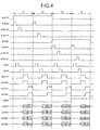
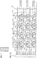
- FIG. 4 is a timing chart illustrating the drive timing of the imaging unit 20.
- FIG. 4 illustrates timings of, in order from the top, a row selection pulse ⁇ X ⁇ 1>, a drive pulse ⁇ R ⁇ 1>, a drive pulse ⁇ T1 ⁇ 1>, a drive pulses ⁇ T2 ⁇ 1>, a row selection pulse ⁇ X ⁇ 2>, a drive pulses ⁇ R ⁇ 2>, a drive pulse ⁇ T1 ⁇ 2>, a drive pulse ⁇ T2 ⁇ 2>, a drive pulse ⁇ NS, a drive pulse ⁇ SS, column selection pulses ⁇ H ⁇ 1> to ⁇ 4>, a drive pulse ⁇ SW, a ⁇ VH1 indicating the type of the signal transferred to the first horizontal transfer line 259, a ⁇ VH2 indicating the type of the signal transferred to the third horizontal transfer line 261, a ⁇ VIN1 indicating the type of the signal input to the first output amplifier unit 311, and
- the timing generator 25 sets the row selection pulse ⁇ X ⁇ 1> and the drive pulse ⁇ R ⁇ 1> to the ON state (High).
- the charge conversion reset unit 236 in the first row is turned on to release the signal charge accumulated in the charge converter 233 in the first row, and reset the charge converter 233 in the first row to a predetermined potential.
- the timing generator 25 sets the drive pulse ⁇ R ⁇ 1> to the OFF state (Low), sets the drive pulse ⁇ NS to the ON state (High), causes the first sample-and-hold unit 242 to sample the noise signal input from the charge converter 233 in the first row via the vertical transfer line 239 of the odd number column, and causes the second sample-and-hold unit 243 to sample the noise signal input from the charge converter 233 in the first row via the vertical transfer line 239 of the even number column.
- the timing generator 25 sets the drive pulse ⁇ NS to the OFF state (Low).
- the first sample-and-hold unit 242 completes the sampling of the noise signal in the odd number column of the first row.
- the second sample-and-hold unit 243 completes the sampling of the noise signal in the even number column of the first row.
- the timing generator 25 sets the drive pulse ⁇ T1 ⁇ 1> to the ON state (High) and sets the drive pulse ⁇ SS to the ON state (High).
- the transfer transistors 234 in each of the odd number column and the even number column in the first row are turned ON by receiving the drive pulse ⁇ T1 ⁇ 1> from the timing generator 25 at the gate thereof, transfers the signal charge from the photoelectric conversion element 231 (pixels R11, R15) of the odd number column in the first row to the charge converter 233, and transfers the signal charge from the photoelectric conversion elements 232 (pixels G14 and G18) in the even number column in the first row to the charge converter 233.
- the pixel output switch 238 of the odd number column causes the pixel source follower transistor 237 to output the imaging signal whose voltage is converted by the charge converter 233 to the vertical transfer line 239.
- the pixel output switch 238 of the even number column causes the pixel source follower transistor 237 to output the imaging signal after voltage conversion by the charge converter 233 to the vertical transfer line 239.
- the first sample-and-hold unit 242 samples the imaging signal corresponding to the photoelectric conversion element 231 (pixels R11, R15) in the odd number column of the first row output from the vertical transfer line 239.
- the second sample-and-hold unit 243 samples the imaging signal corresponding to the photoelectric conversion element 232 (pixels G14, G18) in the even number column of the first row output from the vertical transfer line 239.
- the timing generator 25 sets the drive pulse ⁇ SS to the OFF state (Low), then sets the column selection pulse H ⁇ 1> to the ON state, and sets the drive pulse ⁇ SW to the ON state (High).
- the switching unit 245 since the switching unit 245 is in the ON state, each of the imaging signal corresponding to the pixel R11 sampled by the first sample-and-hold unit 242 and the imaging signal corresponding to the pixel R15 is output to the first output amplifier unit 311 via the second horizontal transfer line 260 and the switching unit 245.
- each of the imaging signal corresponding to the pixel G14 sampled by the second sample-and-hold unit 243 and the imaging signal corresponding to the pixel G18 is output to the second output amplifier unit 312 via the fourth horizontal transfer line 262 and the switching unit 245.
- the timing generator 25 controls on/off operation of the drive pulse ⁇ R ⁇ 1>, the drive pulse ⁇ T2 ⁇ 1>, the drive pulse ⁇ NS, and the drive pulse ⁇ SS.
- the first sample-and-hold unit 242 samples the imaging signal corresponding to the photoelectric conversion element 232 (pixels G12 and G16) in the even number column of the first row output from the vertical transfer line 239.
- the second sample-and-hold unit 243 samples the imaging signal corresponding to the photoelectric conversion element 231 (pixels R13 and R17) in the odd number column of the first row output from the vertical transfer line 239.
- the timing generator 25 sets the column selection pulse H ⁇ 1> to the On state and sets the drive pulse ⁇ SW to the OFF state (Low).
- the switching unit 245 since the switching unit 245 is in the OFF state, each of the imaging signal corresponding to the pixel G12 sampled by the first sample-and-hold unit 242 and the imaging signal corresponding to the pixel G16 is output to the second output amplifier unit 312 via the second horizontal transfer line 260 and the switching unit 245. Further, each of the imaging signal corresponding to the pixel R13 sampled by the second sample-and-hold unit 243 and the imaging signal corresponding to the pixel R17 is output to the first output amplifier unit 311 via the fourth horizontal transfer line 262 and the switching unit 245.
- the timing generator 25 sets the row selection pulse ⁇ X ⁇ 1> to the OFF state and sets the row selection pulse X ⁇ 2> to the ON state (High). Thereafter, by controlling on/off operation of the drive pulse ⁇ R ⁇ 2>, the drive pulse ⁇ T1 ⁇ 2>, the drive pulse ⁇ T2 ⁇ 2>, the drive pulse ⁇ NS, the drive pulse ⁇ SS, the column selection pulse ⁇ H ⁇ M> and the drive pulse ⁇ SW, the imaging signal corresponding to the B pixel in the second row is output from the first output amplifier unit 311 and the imaging signal corresponding to the G pixel is output only from the second output amplifier unit 312.
- the timing generator 25 controls the vertical scanning unit 241 so as to output the imaging signals in twice during one horizontal scanning period and output the imaging signals from the photoelectric conversion element 231 and the photoelectric conversion element 232 in which different filters are arranged on the light receiving surfaces.
- the imaging signal corresponding to the R pixel and the imaging signal corresponding to the B pixel are output from the first output amplifier unit 311, and the imaging signal corresponding to the G pixel is output only from the second output amplifier unit 312.
- the transfer destination of the imaging signal transferred to the switching unit 245 from the first horizontal transfer line 259 to the fourth horizontal transfer line 262 is switched to either the first output amplifier unit 311 or the second output amplifier unit 312, it is possible to prevent variations from occurring in the image signal from the pixel in which the filter of the same color is arranged on the light receiving surface.
- the timing generator 25 causes the switching unit 245 to switch the transfer destination of the imaging signal transferred from each of the first horizontal transfer line 259 to the fourth horizontal transfer line 262 so that the imaging signal (imaging signal corresponding to G pixels) output from the photoelectric conversion element 232 in which filters of the same type are arranged on the light receiving surface is transferred to the same second output amplifier unit 312, it is possible to further improve the frame rate while preventing variations between the channels.
- the noise signal and the imaging signal at the reset time are sampled by each of the first sample-and-hold unit 242 and the second sample-and-hold unit 243.
- a CDS circuit may be provided between the unit pixel 230 and the first sample-and-hold unit 242 or the second sample-and-hold unit 243, and the difference between the noise signal and the imaging signal may be sampled.
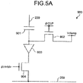
- FIG. 5A is a circuit diagram of a CDS circuit according to a modification of the first embodiment of the present invention.
- a CDS circuit 900 illustrated in FIG. 5A is configured by combining a clamp circuit constituted by a clamp capacitor 901, a clamp switch 902, and a buffer amplifier 903 (for example, a source follower circuit).
- the CDS circuit 900 illustrated in FIG. 5A holds the electric charge corresponding to the noise signal output to the vertical transfer line 239 in the clamp capacitor 901, and then outputs the imaging signal to the vertical transfer line 239, thereby outputting the difference between the noise signal and the imaging signal.
- the timing generator 25 can continuously output the difference between the noise signal and the imaging signal without separately providing a sample-and-hold circuit.
- the switching unit 245 is provided between each of the first horizontal transfer line 259 to the fourth horizontal transfer line 262 and the output unit 31.
- the switching unit 245 is provided for each pixel unit G1 column and for each pixel unit G2 column, so that for example, the imaging signal from the first sample-and-hold unit 242 may be transferred to any one of the first horizontal transfer line 259 to the fourth horizontal transfer line 262.
- the switching unit 245 may be provided between the pixel unit G1 and the first sample-and-hold unit 242 and between the pixel unit G2 and the second sample-and-hold unit 243.
- the endoscope system according to the second embodiment is different from the configuration of the first chip 21 in the endoscope system 1 according to the above-described first embodiment. Specifically, in the first chip 21 according to the above-described first embodiment, one sample-and-hold unit (sample-and-hold circuit) is provided for each pixel unit group. However, in a first chip 21 according to the second embodiment , two sample-and-hold units (sample and hold circuits) are provided for each pixel unit.
- the operation of the imaging unit according to the second embodiment will be described after describing the configuration of the first chip according to the second embodiment.
- the same elements as those of the endoscope system 1 according to the above first embodiment are denoted by the same reference signs, and the explanation thereof is omitted.
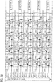
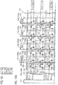
- FIG. 5B is a circuit diagram illustrating a configuration of a first chip according to a second embodiment of the present invention.
- the first chip 21a illustrated in FIG. 5B includes a first sample-and-hold unit 242b and a second sample-and-hold unit 243c in place of each of the first sample-and-hold unit 242 and the second sample-and-hold unit 243 of the first chip 21 according to the above-described first embodiment.
- the first sample-and-hold unit 242b samples the noise signal at the pixel reset time in the unit pixel 230, and outputs the sampled noise signal to the output unit 31. Furthermore, when the drive pulse ⁇ T1 ⁇ M> is applied, the first sample-and-hold unit 242b samples the imaging signal photoelectrically converted by each unit pixel 230, and outputs the sampled imaging signal to the output unit 31.
- the first sample-and-hold unit 242b includes a first sampling switch 251b, a first sampling unit 252b (capacitor), a first output switch 253b, a second sampling switch 254b, a second sampling unit 255b, and a second output switch 256b.
- the first sampling switch 251b has one end connected to the vertical transfer line 239, the other end connected to one end of the first output switch 253b, and a gate connected to a signal line to which the drive pulse ⁇ NS1 is input from the timing generator 25.
- the first sampling unit 252b has one end connected between the first sampling switch 251b and the first output switch 253b and the other end side connected to the ground GND.
- the first sampling unit 252b samples (holds) the noise signal from the unit pixel 230.
- the first output switch 253b has one end connected to the first sampling switch 251b, the other end connected to the third horizontal transfer line 261, and a gate into which the column selection pulse ⁇ H ⁇ M> is input from the horizontal scanning unit 244.
- the first output switch 253b transfers the noise signal sampled by the first sampling unit 252b to the third horizontal transfer line 261.
- the second sampling switch 254b has one end connected to the vertical transfer line 239, the other end connected to one end of the second output switch 256b, and a gate connected to a signal line to which the drive pulse ⁇ SS1 is input from the timing generator 25.
- the second sampling unit 255b has one end connected between the second sampling switch 254b and the second output switch 256b and the other end side connected to the ground GND.
- the second sampling unit 255b samples (holds) the imaging signal from the unit pixel 230.
- the second output switch 256b has one end connected to the second sampling switch 254b, the other end connected to the fourth horizontal transfer line 262, and a gate into which the column selection pulse ⁇ H ⁇ M> is input from the horizontal scanning unit 244.
- the second output switch 256b transfers the imaging signal sampled by the second sampling unit 255b to the horizontal transfer line.
- the second sample-and-hold unit 243c (sample-and-hold circuit) has the same configuration as the first sample-and-hold unit 242b, and when the drive pulse ⁇ R ⁇ M> is applied, samples the noise signal at the pixel reset time in each unit pixel 230, and outputs the sampled noise signal to the output unit 31. Furthermore, when the drive pulse ⁇ T2 ⁇ M> is applied, the second sample-and-hold unit 243c samples the imaging signal photoelectrically converted by each unit pixel 230, and outputs the sampled imaging signal to the output unit 31.
- the second sample-and-hold unit 243c includes a first sampling switch 251c, a first sampling unit 252c (capacitor), a first output switch 253c, a second sampling switch 254c, a second sampling unit 255c, and a second output switch 256c.
- the first sampling switch 251c has one end connected to the vertical transfer line 239, the other end connected to one end of the first output switch 253c, and a gate connected to a signal line to which the drive pulse ⁇ NS2 is input from the timing generator 25.
- the first sampling unit 252c has one end connected between the first sampling switch 251c and the first output switch 253c, and the other end connected to the ground GND.
- the first sampling unit 252c samples (holds) the noise signal from the unit pixel 230.
- the first output switch 253c has one end connected to the first sampling switch 251c, the other end connected to the first horizontal transfer line 259, and a gate into which the column selection pulse ⁇ H ⁇ M> is input from the horizontal scanning unit 244.
- the first output switch 253c transfers the noise signal sampled by the first sampling unit 252c to the horizontal transfer line.
- the second sampling switch 254c has one end connected to the vertical transfer line 239, the other end connected to one end of the second output switch 256c, and a gate connected to a signal line to which the drive pulse ⁇ SS2 is input from the timing generator 25.
- the second sampling unit 255c has one end connected between the second sampling switch 254c and the second output switch 256c, and the other end connected to the ground GND.
- the second sampling unit 255c samples (holds) the imaging signal from the unit pixel 230.
- the second output switch 256c has one end connected to the second sampling switch 254c, the other end connected to the second horizontal transfer line 260, and a gate into which the column selection pulse ⁇ H ⁇ M> is input from the horizontal scanning unit 244.
- the first output switch 256c transfers the imaging signal sampled by the second sampling unit 255c to the horizontal transfer line.
- FIG. 6 is a timing chart illustrating the drive timing of the imaging unit 20.
- FIG. 6 illustrates timings of, in order from the top, a row selection pulse ⁇ X ⁇ 1>, a drive pulse ⁇ R ⁇ 1>, a drive pulse ⁇ T1 ⁇ 1>, a drive pulses ⁇ T2 ⁇ 1>, a row selection pulse ⁇ X ⁇ 2>, a drive pulses ⁇ R ⁇ 2>, a drive pulse ⁇ T1 ⁇ 2>, a drive pulse ⁇ T2 ⁇ 2>, a drive pulse ⁇ NS1, a drive pulse ⁇ SS1, a drive pulse ⁇ NS2, a drive pulse ⁇ SS2, column selection pulses ⁇ H ⁇ 1> to ⁇ 4>, a drive pulse ⁇ SW, a ⁇ VH1 indicating the type of the signal transferred to the first horizontal transfer line 259, a ⁇ VH2 indicating the type of the signal transferred to the third horizontal transfer line 261, a ⁇ VIN1
- the timing generator 25 sets the row selection pulse ⁇ X ⁇ 1> and the drive pulse ⁇ R ⁇ 1> to the ON state (High).
- the charge conversion reset unit 236 in the first row is turned on to release the signal charge accumulated in the charge converter 233 in the first row, and reset the charge converter 233 in the first row to a predetermined potential.
- the timing generator 25 sets the drive pulse ⁇ R ⁇ 1> to the OFF state (Low), sets the drive pulse ⁇ NS1 to the ON state (High), and causes the first sample-and-hold unit 242b to sample the noise signal input from the charge converter 233 in the first row via the vertical transfer line 239.
- the timing generator 25 sets the drive pulse ⁇ NS1 to the OFF state (Low). As a result, the sampling of the noise signal in the first row of the first sample-and-hold unit 242b is completed.
- the timing generator 25 sets the drive pulse ⁇ T1 ⁇ 1> to the ON state (High).
- the transfer transistors 234 in each of the odd number column and the even number column in the first row are turned ON by receiving the drive pulse ⁇ T1 ⁇ 1> from the timing generator 25 at the gate thereof, transfers the signal charge from the photoelectric conversion element 231 (pixels R11, R15) of the odd number column in the first row to the charge converter 233, and transfers the signal charge from the photoelectric conversion elements 232 (pixels G14 and G18) in the even number column in the first row to the charge converter 233.
- the pixel output switch 238 of the odd number column causes the pixel source follower transistor 237 to output the imaging signal whose voltage is converted by the charge converter 233 to the vertical transfer line 239.
- the pixel output switch 238 of the even number column causes the pixel source follower transistor 237 to output the imaging signal after voltage conversion by the charge converter 233 to the vertical transfer line 239.
- the first sample-and-hold unit 242b samples the imaging signal corresponding to the photoelectric conversion element 231 and the photoelectric conversion element 232 (pixels R11, R15, G14, G18) of the first row output from the vertical transfer line 239.
- the timing generator 25 sets the drive pulse ⁇ SS1 to the OFF state (Low), then sets the column selection pulse H ⁇ 1> to the ON state, and sets the drive pulse ⁇ SW to the ON state (High).
- the switching unit 245 since the switching unit 245 is in the ON state, each of the imaging signals corresponding to the pixel R11 sampled by the first sample-and-hold unit 242b and the imaging signal corresponding to the pixel R15 is output to the second output amplifier unit 312 via the fourth horizontal transfer line 262 and the switching unit 245.
- each of the imaging signals corresponding to the pixel G14 sampled by the first sample-and-hold unit 242b and the imaging signal corresponding to the pixel G18 is output to the first output amplifier unit 311 via the second horizontal transfer line 260 and the switching unit 245.
- the timing generator 25 controls on/off operations of the drive pulse ⁇ R ⁇ 1>, the drive pulse ⁇ T2 ⁇ 1>, the drive pulse ⁇ NS2, and the drive pulse ⁇ SS2.
- the second sample-and-hold unit 243c samples the imaging signal corresponding to the photoelectric conversion element 231 (pixels R13, R17) in the odd number column of the first row output from the vertical transfer line 239.
- the second sample-and-hold unit 243c samples the imaging signal corresponding to the photoelectric conversion element 232 (pixels G12, G16) in the even number column of the first row output from the vertical transfer line 239.
- the timing generator 25 sets the column selection pulse H ⁇ 3> to the ON state (High).
- the switching unit 245 since the switching unit 245 is in the ON state, each of the imaging signals corresponding to the pixel R13 sampled by the second sample-and-hold unit 243c and the imaging signal corresponding to the pixel R17 is output to the second output amplifier unit 312 via the fourth horizontal transfer line 262 and the switching unit 245.
- each of the imaging signals corresponding to the pixel G12 sampled by the second sample-and-hold unit 243c and the imaging signal corresponding to the pixel G16 is output to the first output amplifier unit 311 via the second horizontal transfer line 260 and the switching unit 245.
- the timing generator 25 controls on/off operations of the row selection pulse ⁇ X ⁇ 2>, the drive pulse ⁇ R ⁇ 2>, the drive pulse ⁇ T1 ⁇ 2>, the drive pulse ⁇ NS1, and the drive pulse ⁇ SS1.
- the first sample-and-hold unit 242b samples the imaging signal corresponding to the photoelectric conversion element 231 (pixels G21 and G25) in the odd number column of the second row output from the vertical transfer line 239.
- the first sample-and-hold unit 242b samples the imaging signal corresponding to the photoelectric conversion element 232 (pixels B24 and B28) in the even number column of the second row output from the vertical transfer line 239.
- the timing generator 25 sets the drive pulse ⁇ SS1 to the OFF state (Low), then sets the column selection pulse H ⁇ 1> to the ON state (High), and sets the drive pulse ⁇ SW to the OFF state (Low).
- the switching unit 245 since the switching unit 245 is in the OFF state, each of the imaging signals corresponding to the pixel B24 sampled by the first sample-and-hold unit 242b and the imaging signal corresponding to the pixel B28 is output to the second output amplifier unit 312 via the second horizontal transfer line 260 and the switching unit 245.
- each of the imaging signals corresponding to the pixel G21 sampled by the first sample-and-hold unit 242b and the imaging signal corresponding to the pixel G25 is output to the first output amplifier unit 311 via the fourth horizontal transfer line 262 and the switching unit 245.
- the timing generator 25 controls the on/off operation of the drive pulse ⁇ R ⁇ 2>, the drive pulse ⁇ T2 ⁇ 2>, the drive pulse ⁇ NS2, and the drive pulse ⁇ SS2.
- the second sample-and-hold unit 243c samples the imaging signal corresponding to the photoelectric conversion element 231 (pixels G23 and G27) in the odd number column of the second row output from the vertical transfer line 239.
- the second sample-and-hold unit 243c samples the imaging signal corresponding to the photoelectric conversion element 232 (pixels B22 and B26) in the even number column of the second row output from the vertical transfer line 239.
- the timing generator 25 controls the vertical scanning unit 241 so as to output the imaging signals in twice during one horizontal scanning period and output the imaging signals from the photoelectric conversion element 231 and the photoelectric conversion element 232 in which different filters are arranged on the light receiving surfaces.
- the imaging signal corresponding to the R pixel and the imaging signal corresponding to the B pixel are output from the second output amplifier unit 312.
- the imaging signal corresponding to the G pixel is output only from the first output amplifier unit 311.
- the transfer destination of the imaging signal transferred to the switching unit 245 from the first horizontal transfer line 259 to the fourth horizontal transfer line 262 is switched to either the first output amplifier unit 311 or the second output amplifier unit 312, it is possible to prevent variations from occurring in the image signal from the pixel in which the filter of the same color is arranged on the light receiving surface.
- the timing generator 25 when the timing generator 25 causes the pixel unit G1 and the pixel unit G2 to output an imaging signal to the first sample-and-hold unit 242b and the second sample-and-hold unit 243c, by controlling the vertical scanning unit 241 so as to output the imaging signals in twice during one horizontal scanning period and output the imaging signals from the photoelectric conversion element 231 and the photoelectric conversion element 232 in which different filters are arranged on the light receiving surfaces, the timing generator 25 causes the second output amplifier unit 312 to output the imaging signal corresponding to the R pixel and the imaging signal corresponding to the B pixel, and the timing generator 25 causes the first output amplifier unit 311 to output only the imaging signal corresponding to the G pixel; therefore, since all the reading periods of one row can be assigned to horizontal scanning, it is possible to improve the frame rate without increasing the speed of the first output amplifier unit 311 and the second output amplifier unit 312.
- the switching unit 245 is provided between each horizontal transfer line and the output unit 31; however, in the modification of the second embodiment, the switching unit is provided between each sample-and-hold unit and each horizontal transfer line.
- the configuration of the first chip according to the modification of the second embodiment will be described.
- the same elements as those of the endoscope system 1 according to the above second embodiment are denoted by the same reference signs, and the explanation thereof is omitted.
- FIG. 7 is a circuit diagram illustrating a configuration of a first chip according to a modification of the second embodiment of the present invention.
- the first chip 21b illustrated in FIG. 7 includes a plurality of switching units 600 provided in each pixel unit group and switching the output of the imaging signal output from the first sample-and-hold unit 242b and the second sample-and-hold unit 243c.
- the switching unit 600 has the same configuration as the switching unit 245 according to the above-described second embodiment, and based on the drive pulse ⁇ SW input from the timing generator 25, outputs the imaging signal output from the first sample-and-hold unit 242b and the second sample-and-hold unit 243c to the second horizontal transfer line 260 or the fourth horizontal transfer line 262. For example, when the imaging signal corresponding to the R pixel and the imaging signal corresponding to the B pixel are output from the first sample-and-hold unit 242b, the switching unit 600 connects the first sample-and-hold unit 242b and the fourth horizontal transfer line 262, and outputs each of the imaging signal corresponding to the R pixel and the imaging signal corresponding to the B pixel to the second output amplifier unit 312.
- the switching unit 600 connects the first sample-and-hold unit 242b and the second horizontal transfer line 260, and outputs the imaging signal corresponding to the G pixel to the first output amplifier unit 311.
- the switching unit 600 is provided between the sample-and-hold unit and the horizontal transfer line.
- the switching unit 600 may be provided between the unit pixel 230 and the sample-and-hold unit.
- the endoscope system according to the third embodiment is different from the configuration of the first chip 21a in the endoscope system 1 according to the above-described second embodiment.
- the output unit 31 amplifies the imaging signal and outputs the amplified imaging signal to the outside.
- the first chip according to the third embodiment performs a sampling operation in which the output unit holds the imaging signal, and an A/D conversion operation (processing operation) for A/D converting the sampled imaging signal.
- the operation of the imaging unit according to the third embodiment will be described after describing the configuration of the first chip according to the third embodiment.
- the same elements as those of the endoscope system 1 according to the above second embodiment are denoted by the same reference sings, and the explanation thereof is omitted.
- FIG. 8 is a circuit diagram illustrating the configuration of the first chip according to the third embodiment of the present invention.
- the first chip 21c illustrated in FIG. 8 includes a switching unit 610 and an output unit 400 in place of the switching unit 245 and the output unit 31 of the first chip 21a according to the above-described second embodiment.
- the third horizontal transfer line 261 and the fourth horizontal transfer line 262 are omitted from the configuration of the first chip 21a according to the above-described second embodiment, and the second sample-and-hold unit 243 c is connected to the first horizontal transfer line 259 and the second horizontal transfer line 260.
- the switching unit 610 connects the first horizontal transfer line 259 and the second horizontal transfer line 260 to one of a first ADC unit 401 and a second ADC unit 402 of the output unit 400 to be described later.
- the switching unit 610 includes the first selection switch 245a, the second selection switch 245b, a third selection switch 245i, and a fourth selection switch 245j .
- the third selection switch 245i has one end connected to the first horizontal transfer line 259, the other end side connected to the second ADC unit 402 of the output unit 400 to be described later, and a gate connected to a signal line into which a drive pulse ⁇ SW is applied from the timing generator 25.
- the fourth selection switch 245j has one end connected to the second horizontal transfer line 260, the other end side connected to the second ADC unit 402 of the output unit 400 to be described later, and a gate connected to a signal line into which a drive pulse ⁇ SW is applied from the timing generator 25.
- the output unit 400 samples the imaging signal input from the first horizontal transfer line 259 or the second horizontal transfer line 260 via the switching unit 600 and performs A/D conversion on the sampled imaging signal, generates a digital imaging signal, and outputs the digital imaging signal to the outside.
- the output unit 400 includes the first ADC unit 401 and the second ADC unit 402.
- the first ADC unit 401 samples the imaging signal input from the first horizontal transfer line 259, performs A/D conversion on the sampled imaging signal, generates a digital imaging signal, and outputs the digital imaging signal to the outside (Vout1).
- the second ADC unit 402 samples the imaging signal input from the second horizontal transfer line 260, performs A/D conversion on the sampled imaging signal, generates a digital imaging signal, and outputs the digital imaging signal to the outside (Vout2).
- FIG. 9 is a timing chart illustrating the drive timing of the imaging unit 20.
- FIG. 9 illustrates timings of, in order from the top, ⁇ VH1 indicating the type of the signal transferred to the first horizontal transfer line 259, ⁇ VH2 indicating the type of the signal transferred to the second horizontal transfer line 260, ⁇ VIN1 indicating the type of the signal input to the first ADC unit 401, and ⁇ VIN2 indicating the type of the signal input to the second ADC unit 402.
- the imaging unit 20 according to the third embodiment performs the same operation as the imaging unit 20 according to the above-described second embodiment, and only the operations of the switching unit 610 and the output unit 400 are different. Since the other operation is the same as that of the above-described second embodiment, description thereof will be omitted.
- the timing generator 25 performs on/off operation of the column selection pulse ⁇ H ⁇ M> and controls the horizontal scanning unit 244. Accordingly, the imaging signal (R pixel) corresponding to the pixel R11 and the imaging signal (G pixel) corresponding to the pixel G14 are alternately read out by selecting the first sample-and-hold unit 242b or the second sample-and-hold unit 243c from which the imaging signal is read out.
- the switching unit 610 switches, the imaging signal input from the first horizontal transfer line 259 or the second horizontal transfer line 260 to the first ADC unit 401 or the second ADC unit 402 and output the imaging signal.
- the first ADC unit 401 or the second ADC unit 402 performs the sampling operation of the input signal in one of the input signal ⁇ VIN1 and the input signal ⁇ VIN2, performs the A/D conversion operation in the other period, and output the signal.
- the timing generator 25 when the timing generator 25 causes the pixel unit G1 and the pixel unit G2 to output an imaging signal to the first sample-and-hold unit 242b and the second sample-and-hold unit 243c, by controlling the vertical scanning unit 241 so as to output the imaging signals in twice during one horizontal scanning period and output the imaging signals from the photoelectric conversion element 231 and the photoelectric conversion element 232 in which different filters are arranged on the light receiving surfaces, the timing generator 25 causes the first ADC unit 401 to output the imaging signal corresponding to the R pixel and the imaging signal corresponding to the B pixel, and the timing generator 25 causes the second ADC unit 402 to output only the imaging signal corresponding to the G pixel; therefore, since all the reading periods of one row can be assigned to horizontal scanning, it is possible to improve the frame rate without increasing the speed of the first ADC unit 401 and the second ADC unit 402.
- each of the first amplifier for amplifying the digital imaging signal output from the first ADC unit 401 and the second amplifier for amplifying the digital imaging signal output from the second ADC unit 402 may be provided.
- the endoscope system according to the fourth embodiment is different from the configuration of the first chip 21a in the endoscope system 1 according to the above-described second embodiment. Specifically, in the second embodiment, two imaging signals are simultaneously read out from one row and two columns (two photoelectric conversion elements) (two-channel output); however, in the fourth embodiment, four imaging signals are simultaneously read out from two rows and two columns (four photoelectric conversion elements) (4 channel output).
- the configuration of the first chip in the endoscope system according to the fourth embodiment will be described.
- FIG. 10 is a circuit diagram illustrating the configuration of the first chip according to the fourth embodiment of the present invention.
- a first chip 21d illustrated in FIG. 10 includes a first sample-and-hold unit 242d, a second sample-and-hold unit 243e, a switching unit 500, a horizontal reset unit 246d, and an output unit 31d.
- the first chip 21d has a third sample-and-hold unit 242f, a fourth sample-and-hold unit 243g, a fifth horizontal transfer line 263, a sixth horizontal transfer line 264, a seventh horizontal transfer line 265, and an eighth horizontal transfer line 266.
- the first sample-and-hold unit 242d samples the noise signal at the time of pixel reset in each unit pixel 230 which outputs the imaging signal via the vertical transfer line 239 of the odd number row and the odd number column, and outputs the sampled noise signal to the first horizontal transfer line 259. Furthermore, the first sample-and-hold unit 242d samples the imaging signal photoelectrically converted by each unit pixel 230 that outputs the imaging signal via the vertical transfer line 239 of the odd number row and the odd number column and outputs the sampled imaging signal to the second horizontal transfer line 260.
- the first sample-and-hold unit 242d includes the first sampling switch 251, the first sampling unit 252, the first output switch 253, the second sampling switch 254, the second sampling unit 255, and the second output switch 256.
- the second sample-and-hold unit 243e samples the noise signal at the time of pixel reset in each unit pixel 230 that outputs the imaging signal via the vertical transfer line 239 of the even number row and the odd number column and outputs the sampled noise signal to the third horizontal transfer line 261. Furthermore, the second sample-and-hold unit 243e samples the imaging signal photoelectrically converted by each unit pixel 230 that outputs the imaging signal via the vertical transfer line 239 of the even number row and the odd number column and outputs the sampled imaging signal to the fourth horizontal transfer line 262.
- the second sample-and-hold unit 243e includes the first sampling switch 251a, the first sampling unit 252a, the first output switch 253a, the second sampling switch 254a, the second sampling unit 255a, and the second output switch 256a.
- the third sample-and-hold unit 242f samples the noise signal at the time of pixel reset in each unit pixel 230 that outputs the imaging signal via the vertical transfer line 239 of the odd number row and the even number column and outputs the sampled noise signal to the fifth horizontal transfer line 263. Furthermore, the third sample-and-hold unit 242f samples the imaging signal photoelectrically converted by each unit pixel 230 that outputs the imaging signal via the vertical transfer line 239 of the odd number row and the even number column and outputs the sampled imaging signal to the sixth horizontal transfer line 264.
- the third sample-and-hold unit 242f includes the first sampling switch 251, the first sampling unit 252, the first output switch 253, the second sampling switch 254, the second sampling unit 255, and the second output switch 256.
- the fourth sample-and-hold unit 243g samples the noise signal at the time of pixel reset in each unit pixel 230 that outputs the imaging signal via the vertical transfer line 239 of the even number row and the even number column and outputs the sampled noise signal to the seventh horizontal transfer line 265. Furthermore, the fourth sample-and-hold unit 243g samples the imaging signal photoelectrically converted by each unit pixel 230 that outputs the imaging signal via the vertical transfer line 239 of the even number row and the even number column and outputs the sampled imaging signal to the eighth horizontal transfer line 266.
- the fourth sample-and-hold unit 243g includes the first sampling switch 251a, the first sampling unit 252a, the first output switch 253a, the second sampling switch 254a, the second sampling unit 255a, and the second output switch 256a.
- the switching unit 500 connects the first horizontal transfer line 259 to the fourth horizontal transfer line 262 to one of the first output amplifier unit 311 and the second output amplifier unit 312 of the output unit 31d to be described later, and connects the fifth horizontal transfer line 263 to the eighth horizontal transfer line 266 to one of the third output amplifier unit 313 and the fourth output amplifier unit 314 of the output unit 31d to be described later.
- the switching unit 500 includes a first switching unit 501 and a second switching unit 502.
- the first switching unit 501 connects the first horizontal transfer line 259, the second horizontal transfer line 260, the third horizontal transfer line 261, and the fourth horizontal transfer line 262 to any one of the first output amplifier unit 311 and the second output amplifier unit 312 of the output unit 31d to be described later.
- the first switching unit 501 includes the first selection switch 245a, the second selection switch 245b, the third selection switch 245c, the fourth selection switch 245d, the fifth selection switch 245e, the sixth selection switch 245f, the seventh selection switch 245g, and the eighth selection switch 245h.
- the second switching unit 502 connects the fifth horizontal transfer line 263, the sixth horizontal transfer line 264, the seventh horizontal transfer line 265, and the eighth horizontal transfer line 266 to any one of the third output amplifier unit 313 and the fourth output amplifier unit 314 of the output unit 31d to be described later.
- the second switching unit 502 has the same configuration as the first switching unit 501 and includes a first selection switch 245i, a second selection switch 245j, a third selection switch 245k, a fourth selection switch 2451, a fifth selection switch 245m, a sixth selection switch 245n, a seventh selection switch 245o, an eighth selection switch 245p, and the inversion element 270.
- the horizontal reset unit 246d resets each of the first horizontal transfer line 259 to the eighth horizontal transfer line 266.
- the horizontal reset unit 246d includes a first horizontal reset unit 601 and a second horizontal reset unit 602.
- the first horizontal reset unit 601 includes a first horizontal reset transistor 271, a second horizontal reset transistor 272, a third horizontal reset transistor 273, and a fourth horizontal reset transistor 274.
- the second horizontal reset unit 602 has the same configuration as the first horizontal reset unit 601, and includes a first horizontal reset transistor 271a, a second horizontal reset transistor 272a, a third horizontal reset transistor 273a, and a fourth horizontal reset transistor 274a.
- the first horizontal reset transistor 271a has one end connected to a reference voltage VREF, the other end connected to the fifth horizontal transfer line 263, and a gate connected to a signal line into which the drive pulse ⁇ hclr is input from the timing generator 25.
- the drive pulse ⁇ hclr is input to the gate of the first horizontal reset transistor 271a from the timing generator 25, the first horizontal reset transistor 271a is turned ON to reset the fifth horizontal transfer line 263.
- the second horizontal reset transistor 272a has one end connected to a reference voltage VREF, the other end connected to the sixth horizontal transfer line 264, and a gate connected to a signal line into which the drive pulse ⁇ hclr is input from the timing generator 25.
- the second horizontal reset transistor 272a is turned ON to reset the sixth horizontal transfer line 264.
- the third horizontal reset transistor 273a has one end connected to a reference voltage VREF, the other end connected to the seventh horizontal transfer line 265, and a gate connected to a signal line into which the drive pulse ⁇ hclr is input from the timing generator 25.
- the third horizontal reset transistor 273a is turned ON to reset the seventh horizontal transfer line 265.
- the fourth horizontal reset transistor 274a has one end connected to the reference voltage VREF, the other end connected to the eighth horizontal transfer line 266, and a gate connected to a signal line into which the drive pulse ⁇ hclr is input from the timing generator 25.
- the drive pulse ⁇ hclr is input to the gate of the fourth horizontal reset transistor 274a from the timing generator 25, the fourth horizontal reset transistor 274a is turned ON to reset the eighth horizontal transfer line 266.
- the output unit 31d takes the difference between the noise signal and the imaging signal transferred from each of the first horizontal transfer line 259 to the eighth horizontal transfer line 266 via the switching unit 500, thereby outputting the imaging signal in which a noise has been removed, to the outside.
- the output unit 31d includes the first output amplifier unit 311, the second output amplifier unit 312, the third output amplifier unit 313, and the fourth output amplifier unit 314.
- the third output amplifier unit 313 is configured using a differential amplifier.
- the third output amplifier unit 313 takes the difference between the imaging signal transferred from the fifth horizontal transfer line 263 via the switching unit 500 and the noise signal transferred from the sixth horizontal transfer line 264, thereby outputting the imaging signal in which a noise has been removed, to the outside (Vout12).
- the fourth output amplifier unit 314 is configured using a differential amplifier, and takes the difference between the imaging signal of the even number column transferred from the seventh horizontal transfer line 265 and the noise signal of the even number column transferred from the eighth horizontal transfer line 266, thereby outputting the imaging signal of the even number column from which noise has been removed, to the outside (Vout11).
- the first chip 21d configured in this way performs the same operation as in the above-described first embodiment, thereby simultaneously outputting the imaging signals of two rows and two columns.
- the timing generator 25 controls the on/off control of the drive pulse ⁇ SW to output imaging signals of the same spectrum (same color filter) from the first output amplifier unit 311 to the fourth output amplifier unit 314.
- the first output amplifier unit 311 outputs the imaging signal corresponding to the R pixel
- the second output amplifier unit 312 outputs the imaging signal corresponding to the G pixel
- the third output amplifier unit 313 outputs the imaging signal corresponding to the B pixel
- the fourth output amplifier unit 314 outputs the imaging signal corresponding to G pixels.
- the switching unit 500 is controlled to cause the first output amplifier unit 311 to output the imaging signal corresponding to the R pixel, cause the second output amplifier unit 312 to output the imaging signal corresponding to the G pixel, cause the third output amplifier unit 313 to output the imaging signal corresponding to the B pixel, and cause the fourth output amplifier unit 314 to output the imaging signal corresponding to the G pixel. Therefore, in comparison with the case where the imaging signal from the photoelectric conversion element 231 and the photoelectric conversion element 232 each of which is provided with the filter of the same color are processed by one signal processing circuit, it is possible to prevent variations among channels.
- the endoscope configured to be inserted into the subject is employed.
- a capsule endoscope or an imaging device for imaging a subject may also be employed, for example.
- the vertical transfer line shares two pixels in the above embodiments
- a vertical transfer line for sharing four pixels or eight pixels may also be employed.
- output amplifiers may be provided in line with the number of shared pixels. Specifically, if one vertical transfer line shares four pixels, four output amplifiers may be provided (four output channels may be provided).
- a plurality of pixels is shared in the row direction in the above embodiments, a plurality of pixels may be shared in the column direction, for example.
Landscapes
- Engineering & Computer Science (AREA)
- Multimedia (AREA)
- Signal Processing (AREA)
- Health & Medical Sciences (AREA)
- Life Sciences & Earth Sciences (AREA)
- Physics & Mathematics (AREA)
- Surgery (AREA)
- Optics & Photonics (AREA)
- Biomedical Technology (AREA)
- General Health & Medical Sciences (AREA)
- Radiology & Medical Imaging (AREA)
- Nuclear Medicine, Radiotherapy & Molecular Imaging (AREA)
- Biophysics (AREA)
- Heart & Thoracic Surgery (AREA)
- Medical Informatics (AREA)
- Molecular Biology (AREA)
- Animal Behavior & Ethology (AREA)
- Pathology (AREA)
- Public Health (AREA)
- Veterinary Medicine (AREA)
- Astronomy & Astrophysics (AREA)
- General Physics & Mathematics (AREA)
- Transforming Light Signals Into Electric Signals (AREA)
- Endoscopes (AREA)
- Color Television Image Signal Generators (AREA)
- Solid State Image Pick-Up Elements (AREA)
Applications Claiming Priority (2)
| Application Number | Priority Date | Filing Date | Title |
|---|---|---|---|
| JP2015197006 | 2015-10-02 | ||
| PCT/JP2016/078287 WO2017057282A1 (ja) | 2015-10-02 | 2016-09-26 | 撮像素子および内視鏡 |
Publications (2)
| Publication Number | Publication Date |
|---|---|
| EP3358828A1 true EP3358828A1 (de) | 2018-08-08 |
| EP3358828A4 EP3358828A4 (de) | 2019-03-13 |
Family
ID=58427470
Family Applications (1)
| Application Number | Title | Priority Date | Filing Date |
|---|---|---|---|
| EP16851453.7A Withdrawn EP3358828A4 (de) | 2015-10-02 | 2016-09-26 | Bildaufnahmeelement und endoskop |
Country Status (5)
| Country | Link |
|---|---|
| US (1) | US20170311787A1 (de) |
| EP (1) | EP3358828A4 (de) |
| JP (1) | JP6138401B1 (de) |
| CN (1) | CN107113386A (de) |
| WO (1) | WO2017057282A1 (de) |
Families Citing this family (2)
| Publication number | Priority date | Publication date | Assignee | Title |
|---|---|---|---|---|
| WO2018123174A1 (ja) * | 2016-12-28 | 2018-07-05 | オリンパス株式会社 | 撮像装置、内視鏡および内視鏡システム |
| US10270992B1 (en) * | 2017-11-30 | 2019-04-23 | Taiwan Semiconductor Manufacturing Co., Ltd. | Sampling device and method for reducing noise |
Family Cites Families (13)
| Publication number | Priority date | Publication date | Assignee | Title |
|---|---|---|---|---|
| US6734906B1 (en) * | 1998-09-02 | 2004-05-11 | Canon Kabushiki Kaisha | Image pickup apparatus with photoelectric conversion portions arranged two dimensionally |
| CN1203665C (zh) * | 2002-03-25 | 2005-05-25 | 精工爱普生株式会社 | 固体摄像元件以及使用其的固体摄像装置 |
| US20050062866A1 (en) * | 2003-09-23 | 2005-03-24 | Ang Lin Ping | Multiplexed pixel column architecture for imagers |
| JP2005109968A (ja) * | 2003-09-30 | 2005-04-21 | Matsushita Electric Ind Co Ltd | カラー固体撮像装置 |
| JP4419707B2 (ja) * | 2004-06-24 | 2010-02-24 | ソニー株式会社 | 増幅型固体撮像装置 |
| US7652703B2 (en) * | 2004-07-12 | 2010-01-26 | Micron Technology, Inc. | Dual panel pixel readout in an imager |
| KR101073794B1 (ko) * | 2004-08-31 | 2011-10-13 | 인텔렉츄얼 벤처스 투 엘엘씨 | Cmos 이미지 센서 |
| TWI278232B (en) * | 2004-08-31 | 2007-04-01 | Magnachip Semiconductor Ltd | CMOS image sensor |
| JP4425809B2 (ja) * | 2005-02-03 | 2010-03-03 | 富士通マイクロエレクトロニクス株式会社 | 撮像装置 |
| JP4978136B2 (ja) * | 2005-09-28 | 2012-07-18 | ソニー株式会社 | 固体撮像素子及び固体撮像装置 |
| JP4661912B2 (ja) * | 2008-07-18 | 2011-03-30 | ソニー株式会社 | 固体撮像素子およびカメラシステム |
| JP5596888B1 (ja) * | 2013-01-23 | 2014-09-24 | オリンパスメディカルシステムズ株式会社 | 撮像装置、内視鏡システム及びノイズ除去方法 |
| JP6265694B2 (ja) * | 2013-11-12 | 2018-01-24 | キヤノン株式会社 | 固体撮像装置及び撮像システム |
-
2016
- 2016-09-26 EP EP16851453.7A patent/EP3358828A4/de not_active Withdrawn
- 2016-09-26 WO PCT/JP2016/078287 patent/WO2017057282A1/ja not_active Ceased
- 2016-09-26 CN CN201680005647.0A patent/CN107113386A/zh active Pending
- 2016-09-26 JP JP2017509071A patent/JP6138401B1/ja active Active
-
2017
- 2017-07-20 US US15/654,797 patent/US20170311787A1/en not_active Abandoned
Also Published As
| Publication number | Publication date |
|---|---|
| JPWO2017057282A1 (ja) | 2017-10-05 |
| US20170311787A1 (en) | 2017-11-02 |
| EP3358828A4 (de) | 2019-03-13 |
| WO2017057282A1 (ja) | 2017-04-06 |
| JP6138401B1 (ja) | 2017-05-31 |
| CN107113386A (zh) | 2017-08-29 |
Similar Documents
| Publication | Publication Date | Title |
|---|---|---|
| US9191591B2 (en) | Imaging device, endoscope system and method of eliminating noise | |
| CN104272718B (zh) | 固体摄像装置 | |
| CN105101865B (zh) | 摄像元件、摄像装置、内窥镜、内窥镜系统以及摄像元件的驱动方法 | |
| EP2988492B1 (de) | Bildaufnahmeelement, bildaufnahmevorrichtung und endoskopsystem | |
| US9813645B2 (en) | Image sensor, imaging device, endoscope, and endoscopic system | |
| EP3157248B1 (de) | Bildgebungselement, bildgebungsvorrichtung, endoskop, endoskopsystem und verfahren zur ansteuerung eines bildgebungselements | |
| CN104272719B (zh) | 固体摄像装置 | |
| EP3367667A1 (de) | Bildgebungsvorrichtung, endoskop und endoskopsystem | |
| US20180054580A1 (en) | Image sensor and endoscope | |
| EP3236652A1 (de) | Endoskop und endoskopsystem | |
| US9693002B2 (en) | Image sensor, imaging device, endoscope, and endoscope system | |
| EP3358828A1 (de) | Bildaufnahmeelement und endoskop | |
| EP3258492A1 (de) | Bilderfassungselement | |
| US10456023B2 (en) | Image sensor, endoscope, and endoscope system | |
| JP2008078894A (ja) | 光電変換装置 |
Legal Events
| Date | Code | Title | Description |
|---|---|---|---|
| STAA | Information on the status of an ep patent application or granted ep patent |
Free format text: STATUS: THE INTERNATIONAL PUBLICATION HAS BEEN MADE |
|
| PUAI | Public reference made under article 153(3) epc to a published international application that has entered the european phase |
Free format text: ORIGINAL CODE: 0009012 |
|
| STAA | Information on the status of an ep patent application or granted ep patent |
Free format text: STATUS: REQUEST FOR EXAMINATION WAS MADE |
|
| 17P | Request for examination filed |
Effective date: 20180423 |
|
| AK | Designated contracting states |
Kind code of ref document: A1 Designated state(s): AL AT BE BG CH CY CZ DE DK EE ES FI FR GB GR HR HU IE IS IT LI LT LU LV MC MK MT NL NO PL PT RO RS SE SI SK SM TR |
|
| AX | Request for extension of the european patent |
Extension state: BA ME |
|
| DAV | Request for validation of the european patent (deleted) | ||
| DAX | Request for extension of the european patent (deleted) | ||
| A4 | Supplementary search report drawn up and despatched |
Effective date: 20190211 |
|
| RIC1 | Information provided on ipc code assigned before grant |
Ipc: H04N 5/374 20110101AFI20190205BHEP Ipc: H01L 27/146 20060101ALI20190205BHEP Ipc: G02B 23/24 20060101ALI20190205BHEP Ipc: A61B 1/04 20060101ALI20190205BHEP Ipc: H04N 9/07 20060101ALI20190205BHEP Ipc: H01L 27/14 20060101ALI20190205BHEP |
|
| STAA | Information on the status of an ep patent application or granted ep patent |
Free format text: STATUS: THE APPLICATION IS DEEMED TO BE WITHDRAWN |
|
| 18D | Application deemed to be withdrawn |
Effective date: 20190911 |