EP3357152B1 - Method for actuating a multi-phase synchronous converter - Google Patents
Method for actuating a multi-phase synchronous converter Download PDFInfo
- Publication number
- EP3357152B1 EP3357152B1 EP16774685.8A EP16774685A EP3357152B1 EP 3357152 B1 EP3357152 B1 EP 3357152B1 EP 16774685 A EP16774685 A EP 16774685A EP 3357152 B1 EP3357152 B1 EP 3357152B1
- Authority
- EP
- European Patent Office
- Prior art keywords
- output current
- duty cycle
- threshold
- mode
- synchronous converter
- Prior art date
- Legal status (The legal status is an assumption and is not a legal conclusion. Google has not performed a legal analysis and makes no representation as to the accuracy of the status listed.)
- Active
Links
- 230000001360 synchronised effect Effects 0.000 title claims description 54
- 238000000034 method Methods 0.000 title claims description 12
- 230000000903 blocking effect Effects 0.000 claims description 43
- 238000005070 sampling Methods 0.000 claims description 21
- 230000001419 dependent effect Effects 0.000 claims description 3
- 230000008859 change Effects 0.000 description 6
- 230000010355 oscillation Effects 0.000 description 6
- 238000010586 diagram Methods 0.000 description 4
- 238000013459 approach Methods 0.000 description 2
- 230000002457 bidirectional effect Effects 0.000 description 2
- 230000009849 deactivation Effects 0.000 description 2
- 230000007704 transition Effects 0.000 description 2
- YBJHBAHKTGYVGT-ZKWXMUAHSA-N (+)-Biotin Chemical compound N1C(=O)N[C@@H]2[C@H](CCCCC(=O)O)SC[C@@H]21 YBJHBAHKTGYVGT-ZKWXMUAHSA-N 0.000 description 1
- 230000008901 benefit Effects 0.000 description 1
- 239000003990 capacitor Substances 0.000 description 1
- 230000007423 decrease Effects 0.000 description 1
- 230000001934 delay Effects 0.000 description 1
- 238000001914 filtration Methods 0.000 description 1
- 230000009467 reduction Effects 0.000 description 1
- 230000001131 transforming effect Effects 0.000 description 1
- FEPMHVLSLDOMQC-UHFFFAOYSA-N virginiamycin-S1 Natural products CC1OC(=O)C(C=2C=CC=CC=2)NC(=O)C2CC(=O)CCN2C(=O)C(CC=2C=CC=CC=2)N(C)C(=O)C2CCCN2C(=O)C(CC)NC(=O)C1NC(=O)C1=NC=CC=C1O FEPMHVLSLDOMQC-UHFFFAOYSA-N 0.000 description 1
Images

Classifications
-
- H—ELECTRICITY
- H02—GENERATION; CONVERSION OR DISTRIBUTION OF ELECTRIC POWER
- H02M—APPARATUS FOR CONVERSION BETWEEN AC AND AC, BETWEEN AC AND DC, OR BETWEEN DC AND DC, AND FOR USE WITH MAINS OR SIMILAR POWER SUPPLY SYSTEMS; CONVERSION OF DC OR AC INPUT POWER INTO SURGE OUTPUT POWER; CONTROL OR REGULATION THEREOF
- H02M1/00—Details of apparatus for conversion
- H02M1/08—Circuits specially adapted for the generation of control voltages for semiconductor devices incorporated in static converters
- H02M1/088—Circuits specially adapted for the generation of control voltages for semiconductor devices incorporated in static converters for the simultaneous control of series or parallel connected semiconductor devices
-
- H—ELECTRICITY
- H02—GENERATION; CONVERSION OR DISTRIBUTION OF ELECTRIC POWER
- H02M—APPARATUS FOR CONVERSION BETWEEN AC AND AC, BETWEEN AC AND DC, OR BETWEEN DC AND DC, AND FOR USE WITH MAINS OR SIMILAR POWER SUPPLY SYSTEMS; CONVERSION OF DC OR AC INPUT POWER INTO SURGE OUTPUT POWER; CONTROL OR REGULATION THEREOF
- H02M3/00—Conversion of dc power input into dc power output
- H02M3/02—Conversion of dc power input into dc power output without intermediate conversion into ac
- H02M3/04—Conversion of dc power input into dc power output without intermediate conversion into ac by static converters
- H02M3/10—Conversion of dc power input into dc power output without intermediate conversion into ac by static converters using discharge tubes with control electrode or semiconductor devices with control electrode
- H02M3/145—Conversion of dc power input into dc power output without intermediate conversion into ac by static converters using discharge tubes with control electrode or semiconductor devices with control electrode using devices of a triode or transistor type requiring continuous application of a control signal
- H02M3/155—Conversion of dc power input into dc power output without intermediate conversion into ac by static converters using discharge tubes with control electrode or semiconductor devices with control electrode using devices of a triode or transistor type requiring continuous application of a control signal using semiconductor devices only
- H02M3/156—Conversion of dc power input into dc power output without intermediate conversion into ac by static converters using discharge tubes with control electrode or semiconductor devices with control electrode using devices of a triode or transistor type requiring continuous application of a control signal using semiconductor devices only with automatic control of output voltage or current, e.g. switching regulators
- H02M3/158—Conversion of dc power input into dc power output without intermediate conversion into ac by static converters using discharge tubes with control electrode or semiconductor devices with control electrode using devices of a triode or transistor type requiring continuous application of a control signal using semiconductor devices only with automatic control of output voltage or current, e.g. switching regulators including plural semiconductor devices as final control devices for a single load
-
- G—PHYSICS
- G05—CONTROLLING; REGULATING
- G05F—SYSTEMS FOR REGULATING ELECTRIC OR MAGNETIC VARIABLES
- G05F1/00—Automatic systems in which deviations of an electric quantity from one or more predetermined values are detected at the output of the system and fed back to a device within the system to restore the detected quantity to its predetermined value or values, i.e. retroactive systems
- G05F1/10—Regulating voltage or current
- G05F1/46—Regulating voltage or current wherein the variable actually regulated by the final control device is dc
- G05F1/618—Regulating voltage or current wherein the variable actually regulated by the final control device is dc using semiconductor devices in series and in parallel with the load as final control devices
-
- H—ELECTRICITY
- H02—GENERATION; CONVERSION OR DISTRIBUTION OF ELECTRIC POWER
- H02M—APPARATUS FOR CONVERSION BETWEEN AC AND AC, BETWEEN AC AND DC, OR BETWEEN DC AND DC, AND FOR USE WITH MAINS OR SIMILAR POWER SUPPLY SYSTEMS; CONVERSION OF DC OR AC INPUT POWER INTO SURGE OUTPUT POWER; CONTROL OR REGULATION THEREOF
- H02M3/00—Conversion of dc power input into dc power output
- H02M3/02—Conversion of dc power input into dc power output without intermediate conversion into ac
- H02M3/04—Conversion of dc power input into dc power output without intermediate conversion into ac by static converters
- H02M3/10—Conversion of dc power input into dc power output without intermediate conversion into ac by static converters using discharge tubes with control electrode or semiconductor devices with control electrode
- H02M3/145—Conversion of dc power input into dc power output without intermediate conversion into ac by static converters using discharge tubes with control electrode or semiconductor devices with control electrode using devices of a triode or transistor type requiring continuous application of a control signal
- H02M3/155—Conversion of dc power input into dc power output without intermediate conversion into ac by static converters using discharge tubes with control electrode or semiconductor devices with control electrode using devices of a triode or transistor type requiring continuous application of a control signal using semiconductor devices only
- H02M3/156—Conversion of dc power input into dc power output without intermediate conversion into ac by static converters using discharge tubes with control electrode or semiconductor devices with control electrode using devices of a triode or transistor type requiring continuous application of a control signal using semiconductor devices only with automatic control of output voltage or current, e.g. switching regulators
- H02M3/158—Conversion of dc power input into dc power output without intermediate conversion into ac by static converters using discharge tubes with control electrode or semiconductor devices with control electrode using devices of a triode or transistor type requiring continuous application of a control signal using semiconductor devices only with automatic control of output voltage or current, e.g. switching regulators including plural semiconductor devices as final control devices for a single load
- H02M3/1584—Conversion of dc power input into dc power output without intermediate conversion into ac by static converters using discharge tubes with control electrode or semiconductor devices with control electrode using devices of a triode or transistor type requiring continuous application of a control signal using semiconductor devices only with automatic control of output voltage or current, e.g. switching regulators including plural semiconductor devices as final control devices for a single load with a plurality of power processing stages connected in parallel
-
- H—ELECTRICITY
- H02—GENERATION; CONVERSION OR DISTRIBUTION OF ELECTRIC POWER
- H02M—APPARATUS FOR CONVERSION BETWEEN AC AND AC, BETWEEN AC AND DC, OR BETWEEN DC AND DC, AND FOR USE WITH MAINS OR SIMILAR POWER SUPPLY SYSTEMS; CONVERSION OF DC OR AC INPUT POWER INTO SURGE OUTPUT POWER; CONTROL OR REGULATION THEREOF
- H02M1/00—Details of apparatus for conversion
- H02M1/0003—Details of control, feedback or regulation circuits
- H02M1/0025—Arrangements for modifying reference values, feedback values or error values in the control loop of a converter
-
- H—ELECTRICITY
- H02—GENERATION; CONVERSION OR DISTRIBUTION OF ELECTRIC POWER
- H02M—APPARATUS FOR CONVERSION BETWEEN AC AND AC, BETWEEN AC AND DC, OR BETWEEN DC AND DC, AND FOR USE WITH MAINS OR SIMILAR POWER SUPPLY SYSTEMS; CONVERSION OF DC OR AC INPUT POWER INTO SURGE OUTPUT POWER; CONTROL OR REGULATION THEREOF
- H02M1/00—Details of apparatus for conversion
- H02M1/0003—Details of control, feedback or regulation circuits
- H02M1/0032—Control circuits allowing low power mode operation, e.g. in standby mode
-
- Y—GENERAL TAGGING OF NEW TECHNOLOGICAL DEVELOPMENTS; GENERAL TAGGING OF CROSS-SECTIONAL TECHNOLOGIES SPANNING OVER SEVERAL SECTIONS OF THE IPC; TECHNICAL SUBJECTS COVERED BY FORMER USPC CROSS-REFERENCE ART COLLECTIONS [XRACs] AND DIGESTS
- Y02—TECHNOLOGIES OR APPLICATIONS FOR MITIGATION OR ADAPTATION AGAINST CLIMATE CHANGE
- Y02B—CLIMATE CHANGE MITIGATION TECHNOLOGIES RELATED TO BUILDINGS, e.g. HOUSING, HOUSE APPLIANCES OR RELATED END-USER APPLICATIONS
- Y02B70/00—Technologies for an efficient end-user side electric power management and consumption
- Y02B70/10—Technologies improving the efficiency by using switched-mode power supplies [SMPS], i.e. efficient power electronics conversion e.g. power factor correction or reduction of losses in power supplies or efficient standby modes
Definitions
- the present invention deals with a method for controlling a multiphase synchronous converter, consisting of several half-bridges, in turn consisting of an upper power switch and a lower power switch, by means of pulse width modulation depending on a predetermined duty cycle in the range from zero to one hundred percent, with an output current from the synchronous converter is generated and the multiphase synchronous converter is operated in a normal mode in which the circuit breakers switch with a normal switching period defined by a specified normal switching frequency and a normal plus duration dependent on the current duty cycle, whereby as soon as the duty cycle exceeds a first upper duty cycle threshold or falls below a first lower duty cycle threshold, from Normal mode is switched to an operating mode in which at least one of the power switches of at least one half-bridge over a period of time that is greater than the normal switching period, is permanently deactivated.
- DC voltage converters sometimes also called DC voltage transformers
- DC voltage transformers are known for transforming DC voltages into other DC voltage ranges.
- powerful DC voltage converters are required that can also be operated bidirectionally.
- a possible implementation of a bidirectional DC voltage converter is a synchronous converter which represents buck converters, ie which input voltages convert into output voltages less than or at most equal to the input voltages, or vice versa.
- a half-bridge is used for this, the two circuit breakers of the half-bridge being controlled by a controller with pulse width modulation (PWM control) in such a way that they switch alternately with inverted switching pulses within a switching period that is determined by the specified switching frequency.
- PWM control pulse width modulation
- the level of the output voltage of the synchronous converter is set by specifying the duty cycle of the PWM control.
- the duty cycle describes the ratio of the pulse duration of the upper circuit breakers of a half bridge to the switching period.
- These synchronous converters can also be designed as multi-phase converters.
- a plurality of half-bridges, each with two power switches are connected in parallel via the output chokes of the half-bridges and controlled one after the other by the PWM controller.
- the circuit breakers are driven clocked offset by a fraction of the switching period, primarily to reduce output current ripple.
- the output current is determined with a fixed sampling rate.
- the circuit breakers are clocked in each case offset by the switching period divided by the number of half bridges.
- the multi-phase control larger output currents can be generated with a smaller current ripple, or the switching frequency of the total output current of such a multi-phase converter can be reduced, which enables a simpler filter dimensioning.
- smaller capacitors can be used in a polyphase converter for the same power range.
- Controlling the half-bridge with inverting PWM signals basically means that the current can change continuously between positive and negative values within one pulse period. Since both circuit breakers always switch alternately in normal operation, a high or low output voltage cannot be precisely set or achieved, since the voltage is influenced by the required pulses from the other circuit breaker and the dead times generated thereby. This means that no theoretically maximum or minimum possible voltage can be output on the output side without receiving a certain error.
- PWM controls are known that at least enable a duty cycle of 100 percent to be generated, there is a gap for values just under 100 percent.
- the EP 2 439 837 A1 discloses a blocking mode which is activated in the event of so-called "one arm driving", that is to say a deactivation of at least one circuit breaker. The selection of this deactivation is based only on a duty cycle,
- the DE 10 2013 107 792 A1 shows that with a duty cycle in an actually undesirable operating range, the setpoint value of the input voltage is manipulated in such a way that this operating range of the synchronous converter is avoided.
- the US 2013/0229829 A1 shows that the current flowing through the choke cannot have a direct component.
- the burst mode shown also switches with a fixed pulse width, which means that only one fixed operating point can be approached in this operating range.
- This goal is achieved in that there is a second positive output current threshold and a second negative output current threshold, the output current is sampled with a sampling period and, if the output current is less than the second positive output current threshold and greater than the second negative output current threshold, the synchronous converter is in a low-current mode as the operating mode is switched by switching the power switches with a switching period which corresponds to the sampling period increased by a factor z. This reduces the influence of the dead times by the same factor z, since switching takes place z times less often. It is assumed that the upper or lower first duty cycle threshold is exceeded, since otherwise the normal mode would be sufficient.
- the synchronous converter can also be switched to a blocking mode by all lower power switches or all upper power switches, i.e. the respective power switches, which still have short pulses per period in normal mode contribute and thus also cause a dead time, are permanently deactivated.
- “Deactivate” means that the respective circuit breaker is permanently open and no control pulses are applied to it.
- the pulse width of the opposing circuit breaker of the half bridge alone determines the output voltage and there is no need to take into account any dead time between switching the circuit breakers of a half bridge. Since the normal switching period does not change in the blocking mode, the sampling period of the output current can be maintained.
- the upper circuit breakers (with multi-phase synchronous converters actuated offset) can switch permanently, whereas all lower circuit breakers are permanently deactivated during the blocking mode and a duty cycle of one hundred percent is achieved.
- all upper circuit breakers can be deactivated permanently, whereas all lower circuit breakers can be permanently deactivated (in the case of multi-phase synchronous converters, in turn, offset) switch which results in a duty cycle of zero percent. If the output current is negative, the roles of the upper and lower circuit breakers are reversed.
- Output current gaps occur at around zero amperes and oscillations can occur, for example, between the blocking mode for positive current (deactivating all lower circuit breakers) and the blocking mode for negative current (deactivating all upper circuit breakers).
- the normal mode In the case of non-low or non-high duty cycles, the normal mode must therefore be used instead of the blocking mode in order to generate a zero crossing of the output current. In the case of low or high duty cycles, the normal mode again results in the dead time problem mentioned above and the desired duty cycles and thus output voltages cannot be achieved.
- the pulse duration of at least the upper or the lower power switch of a half bridge can be increased by a factor of m from the pulse duration.
- the pulse duration, increased by a factor of m makes it possible to take into account the required dead time for inverting switching of the half-bridge. It is achieved that the pulse widths for the very small output voltages are larger than the dead time and can thus be output. Overall, there is namely a higher totaled total pulse duration over the individual pulses, which occur z times less, but are m times wider.
- the switching half-bridge in the low current mode, for example by increasing the switching period, only one half-bridge switches within a sampling period, i.e. the polyphase synchronous converter is operated like a single-phase synchronous converter, the switching half-bridge changing with each sampling period.
- the current ripple is anyway low at low output currents, so that the omission of nested switching of the half bridges with an increased switching period does not have any disadvantages for the filtering of the output current ripple.
- a half bridge can thus be switched alternately per sampling period.
- the synchronous converter If the synchronous converter is in blocking mode, it can remain in blocking mode if the output current remains greater than a second positive output current threshold or less than a second negative output current threshold, depending on the polarity of the output current.
- the synchronous converter can remain in the low current mode if the output current remains smaller than the first positive output current threshold and larger than the first negative output current threshold.
- the first and second negative output current thresholds or first and second positive output current thresholds can each be set equal.
- the synchronous converter is switched to normal mode.
- the normal mode is active when the upper duty cycle threshold has not been exceeded or the lower duty cycle threshold has not been undershot. Oscillations between normal mode and blocking mode or low-current mode can therefore also occur with regard to the duty cycle if the duty cycle fluctuates around the upper or lower duty cycle threshold.
- a further hysteresis can be generated by setting at least one further duty cycle threshold which is closer to a duty cycle of 50% than the upper or lower duty cycle threshold.
- a non-implementation of the further duty cycle threshold can also be interpreted as a coincidence of further duty cycle threshold and upper or lower duty cycle threshold - whereby the further duty cycle threshold is no longer closer to a duty cycle of 50% than the upper or lower duty cycle threshold.
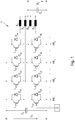
- a known multiphase, here a four-phase, synchronous converter 1 according to the prior art is shown.
- synchronous converters are bidirectional, but the left side is referred to as the input side with the input voltage U 1 at the input capacitance C 1 and the right side as the output side with the output voltage U 2 at the output capacitance C 2 .
- inductances X 1 , X 2 , X 3 , X 4 (chokes) are also provided on the individual phases, the inductances X 1 , X 2 , X 3 , X 4 on the one hand between the upper and lower circuit breakers with each a half bridge HB 1 , HB 2 , HB 3 , HB 4 are connected and on the other hand are connected to one another.
- the inductances X 1 , X 2 , X 3 , X 4 together with the output capacitance C 2 form an output filter of the synchronous converter 1.
- the half bridges HB 1 , HB 2 , HB 3 , HB 4 each consist of an upper circuit breaker L o1 , L o2 , L o3 , L o4 and a lower circuit breaker L u1 , L u2 , L u3 , L u4 and possibly associated diodes D o1 , D u1 , D o2 , D u2 , D o3 , D u3 , D o4 , D u4 .
- a PWM control 2 (in Fig.
- the upper circuit breakers L o1 , L o2 , L o3 , L o4 are switched conductive and meanwhile the respective lower circuit breakers L u1 , L u2 , L u3 , L u4 of the relevant half-bridge HB 1 , HB 2 , HB 3 , HB 4 blocked.
- the previously turned-on upper power switch L O1, L o2, L o3, L o4 be locked in each case and the previously blocked connected lower power switches L u1, L u2 , L u3 , L u4 are switched on.
- the voltage input is short-circuited, after each normal plus duration t o , t u there is a dead time ⁇ t between the switching on / off of the upper circuit breaker L o1 , L o2 , L o3 , L o4 and the switching off / on of the associated lower circuit breaker L u1 , L u2 , L u3 , L u4 of the half-bridge HB 1 , HB 2 , HB 3 , HB 4 and vice versa.
- the ratio of the pulse durations t o , the upper power switches L o1, L o2 , L o3 , L o4 and the pulse durations t u of the lower power switches L u1, L u2 , L u3 , L u4 is thus determined by the PWM controller 2 via the Duty cycle S and the normal duty cycle T 0 are determined.
- the output voltage U 2 is set using the duty cycle S.
- a duty cycle S of one hundred percent would (with a positive output current I a ) mean that the upper circuit breaker L o1 , L o2 , L o3 , L o4 is permanently switched and the lower power switch L u1, L u2 , L u3 , L u4 of all half bridges HB 1 , HB 2 , HB 3 , HB 4 is permanently blocked. This would cause the input voltage U 1 to be switched through to the output voltage U 2 .
- a duty cycle S of zero percent would mean that all lower power switches L u1, L u2 , L u3 , L u4 are permanently switched and the upper power switches L o1 , L o2 , L o3 , L o4 of all half bridges HB 1 , HB 2 , HB 3 , HB 4 are permanently blocked or permanently deactivated. This causes an output voltage U 2 of zero.
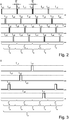
- FIG. 2 the circuit diagram of the circuit breakers L o1, L u1 , L o2 , L u2 , L o3 , L u3 , L o4 , L u4 is shown, with each of the four half bridges HB 1 , HB 2 , HB 3 , HB 4 offset with the Normal switching period T 0 are clocked by the number x of half bridges, so here with T 0/4 .
- x represents the number of half bridges HB 1 HB 2 , HB 3 , HB 4 and i a natural number from 1 to 2x.
- the sampled output current value is required by the PWM controller 2 to control the synchronous converter 1.
- a relatively low duty cycle S is shown, ie the pulse durations t o of the upper circuit breakers L o1 , L o2 , L o3 , L o4 are significantly lower than those Pulse durations t u of the lower power switches L u1, L u2 , L u3 , L u4 .
- the dead time ⁇ t can be seen between the individual pulses.
- the minimum pulse duration t o of the upper circuit breakers L o1 , L o2 , L o3 , L o4 in a normal switching period T 0 is thus due to the minimum required pulse duration t o of the upper circuit breakers L o1 , L o2 , L o3 , L o4 and twice Way limited by the length of the dead time ⁇ t.
- the minimum pulse durations t o , t u of all power switches L o1, L u1 , L o2 , L u2 , L o3 , L u3 , L o4 , L u4 are approximately in the order of magnitude of the dead time ⁇ t .
- Deactivated means that the circuit breaker does not deliver any pulses, i.e. is open, and thus the switching duration of the opposite one Circuit breaker is not reduced by any dead time.
- the dead time ⁇ t which would limit the voltage range, is saved approximately at least three times within a period corresponding to the normal switching period T 0.
- the synchronous converter 1 can be switched to a blocking mode M 1 , M 2 by removing all lower power switches L u1, L u2 , L u3 , L u4 (if I a > I 1+ ) or all upper power switches L o1, L o2 , L o3 , L o4 (if I a ⁇ I 1- ) are permanently deactivated as long as the polyphase synchronous converter 1 is in the blocking mode M 1 , M 2 .
- the output voltage U 2 required by the synchronous converter 1 must require a duty cycle greater than the first upper duty cycle threshold S o1 or lower than the first lower duty cycle threshold S u1, if the upper or lower duty cycle threshold S o1, S u1 has been exceeded or fallen below and the output current I a exceeds, for example, the first positive output current threshold I 1+ , all lower power switches L u1, L u2 , L u3 , L u4 of all half bridges HB 1 , HB 2 , HB 3 , HB 4 are permanently deactivated, which is the blocking mode M 1 leads.
- the upper circuit breakers L o1 , L o2 , L o3 , L o4 continue to switch offset by the normal switching period T 0 by the number of half bridges HB 1 , HB 2 , HB 3 , HB 4 with a pulse duration t o depending on the desired duty cycle S. Es However, there is the advantage that higher and lower pulse durations t o and thus higher and lower duty cycles S than in normal mode M 0 are now made possible. Since the lower power switches L u1, L u2 , L u3 , L u4 do not switch in the blocking mode M 1 , no dead times ⁇ t are required and the pulse durations t o are not restricted.
- this output voltage U 2 is desired. With a positive output current I a, this output voltage U 2 can be set as desired by varying the pulse durations t o of the upper circuit breakers L o1 , L o2 , L o3 , L o4.
- a duty cycle S is thus also possible in a range just below and up to one hundred percent, which would mean that the upper circuit breakers L o1 , L o2 , L o3 , L o4 almost permanently (again offset in the case of a multi-phase synchronous converter 1) or are permanently switched.
- the synchronous converter can 1 can be switched to a low current mode M 3 as the operating mode.
- the power switches L 11 , L 12 , L 21 , L 22 , L 31 , L 32 , L 41 , L 42 are switched with a switching period T 3 which corresponds to the normal switching period T 0 increased by a factor z.
- HB 1 , HB 2 , HB 3 , HB 4 can be switched per scanning period T S , which can be achieved, for example, by suitable selection of the factor z and thus the switching period T 3 .
- a normal switching period T 0 is always at least one of the circuit breakers L o1, L U1, L o2, L u2, L o3, L u 3, L o4, L is disabled u4 in the low current mode M 3, which would be active in normal mode M 0th
- this concerns the power switches L o1, L o2 , L o3
- the pulse durations t o , t u of the power switches L o1, L u1 , L o2 , L u2 , L o3 , L u3 , L o4 , L u4 can be increased by a factor m at the same time.
- the pulse durations t o , t u increased by the factor m make it possible, for example, to output smaller output voltages U 2 for very small duty cycles S, since the relation of pulse durations t o , t u to the dead time ⁇ t improves by the factor m.
- the result is a higher totaled total pulse duration over the individual pulse durations t o , t u , which occur z times less often, but are m times wider.
- the factor m can be chosen to be equal to the factor z, which results in the same duty cycle S (i.e. the same sum of all pulse durations within a normal switching period T 0 ) as in the normal mode M 0 , which ensures that the output current I a is sampled at one point in time in which one phase is in the mean current value. This also means that the sampling of the output current I a does not have to be changed in the low current mode M 3.
- a hysteresis H I + between the first positive output current threshold I 1 + and the second positive output current threshold I 2+ and a hysteresis H I can in each case between the first negative output current threshold I 1- and the second negative output current threshold I 2- can be implemented. It must be provided that the first positive output current threshold I 1+ is greater than the second positive output current threshold I 2+, or the first negative output current threshold I 1- is smaller than the second negative output current threshold I 2- .
- the blocking mode M 1 , M 2 is active (ie the first positive output current threshold I 1+ is exceeded or the first negative output current threshold I 1- was undershot) the output current I a is greater than a second positive output current threshold I 2+ or less than one If the second negative output current threshold I 2- remains, the synchronous converter 1 can therefore remain in the respective blocking mode M 1 , M 2 in accordance with the associated hysteresis H I- , H I +.
- the output current I a crosses the second positive output current threshold I 2+ or the second negative output current threshold I 2- when the blocking mode M 1 , M 2 is active, the output current I a thus approaches zero in terms of magnitude, the low current mode M 3 is activated.
- the output current I a remains smaller than the first positive output current threshold I 1+ and greater than the first negative Output current threshold I 1- , the synchronous converter can therefore remain in the low current mode M 3.
- the low current mode is deactivated and the blocking mode M1 or M3 activated depending on the current direction.
- first positive output current threshold I 1+ corresponds to the second positive output current threshold I 1+ and / or the first negative output current threshold I 1- to the second negative output current threshold I 2- , there is no hysteresis H I + or H I- .
- At least one further hysteresis H S1 , H S2 can be implemented.
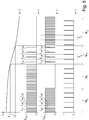
- Fig. 5 shows a profile of the output current I a through the zero crossing and thus the transition from normal mode M 0 first to blocking mode M 1 , then to low current mode M 3 and, in a further line, to blocking mode M 2 .
- normal mode M 0 all of the power switches L o1, L u1 , L o2 , L u2 , L o3 , L u3 , L o4 , L u4 are switched according to a PWM controller 2 corresponding to the prior art. Since the duty cycle S subsequently decreases and the output current I a is positive and sufficiently high, the blocking mode M 1 is activated by deactivating the lower power switches L u1, L u2 , L u3 , L u4.
- the low current mode M 3 is activated while the duty cycle S remains correspondingly low.
- all circuit breakers L o1 , L u1 , L o2 , L u2 , L o3 , L u3 , L o4 , L u4 switch again .
- the switching period T 3 has been increased to z times (here four times) the sampling period T s .
- the pulse durations t o , t u were also increased to an m-fold. It should be noted that the sampling points (bottom graph) of the synchronous converter 1 remain unchanged, ie the sampling rate T S does not change even in the low-current mode M 3 .
Landscapes
- Engineering & Computer Science (AREA)
- Power Engineering (AREA)
- Physics & Mathematics (AREA)
- Electromagnetism (AREA)
- General Physics & Mathematics (AREA)
- Radar, Positioning & Navigation (AREA)
- Automation & Control Theory (AREA)
- Dc-Dc Converters (AREA)
Description
Die gegenständliche Erfindung behandelt ein Verfahren zum Ansteuern eines multiphasigen Synchronwandlers, bestehend aus mehreren Halbbrücken wiederum bestehend aus jeweils einem oberen Leistungsschalter und jeweils einem unteren Leistungsschalter, durch eine Pulsweitenmodulation abhängig von einem vorgegebenen Tastgrad im Bereich von null bis hundert Prozent, wobei vom Synchronwandler ein Ausgangsstrom erzeugt wird und der multiphasige Synchronwandler in einem Normalmodus betrieben wird, in dem die Leistungsschalter mit einer durch eine vorgegebene Normalschaltfrequenz definierte Normalschaltperiode und einer vom aktuellen Tastgrad abhängigen Normalplusdauer schalten, wobei sobald der Tastgrad eine erste obere Tastgradschwelle überschreitet oder eine erste untere Tastgradschwelle unterschreitet, vom Normalmodus in einen Betriebsmodus geschaltet wird, in dem zumindest einer der Leistungsschalter zumindest einer Halbbrücke über einen Zeitraum, der größer als die Normalschaltperiode ist, permanent deaktiviert wird.The present invention deals with a method for controlling a multiphase synchronous converter, consisting of several half-bridges, in turn consisting of an upper power switch and a lower power switch, by means of pulse width modulation depending on a predetermined duty cycle in the range from zero to one hundred percent, with an output current from the synchronous converter is generated and the multiphase synchronous converter is operated in a normal mode in which the circuit breakers switch with a normal switching period defined by a specified normal switching frequency and a normal plus duration dependent on the current duty cycle, whereby as soon as the duty cycle exceeds a first upper duty cycle threshold or falls below a first lower duty cycle threshold, from Normal mode is switched to an operating mode in which at least one of the power switches of at least one half-bridge over a period of time that is greater than the normal switching period, is permanently deactivated.
Um Gleichspannungen in andere Gleichspannungsbereiche zu transformieren sind diverse Gleichspannungswandler, gelegentlich auch Gleichspannungstransformatoren genannt, bekannt. Für bestimmte Anwendungen, wie beispielsweise für Batterieladegeräte oder Batterietestgeräte, sind leistungsfähige Gleichspannungswandler notwendig, die auch bidirektional betrieben werden können. Eine mögliche Realisierung eines bidirektionalen Gleichspannungswandlers stellt ein Synchronwandlers dar, welche Tiefsetzsteller darstellen, d.h. welche Eingangsspannungen in Ausgangsspannungen kleiner oder maximal gleich der Eingangsspannungen wandeln, bzw. umgekehrt. Hierzu wird eine Halbbrücke verwendet, wobei die zwei Leistungsschalter der Halbbrücke von einer Steuerung mit Pulsweitenmodulation (PWM-Steuerung) derart angesteuert werden, dass sie innerhalb einer Schaltperiode, welche durch die vorgegebene Schaltfrequenz festgelegt ist, alternierend mit invertierten Schaltpulsen angesteuert, schalten. Somit ist im Grunde immer ein Leistungsschalter einer Halbbrücke leitend, der andere sperrt. Die Höhe der Ausgangsspannung des Synchronwandlers wird durch die Vorgabe des Tastgrades der PWM-Steuerung eingestellt. Der Tastgrad bezeichnet das Verhältnis der Pulsdauer der oberen Leistungsschalter einer Halbbrücke zur Schaltperiode. Diese Synchronwandler können auch als Mehrphasenwandler ausgeführt werden. In dieser Ausführungsform werden bekanntermaßen mehrere Halbbrücken mit jeweils zwei Leistungsschaltern über die Ausgangsdrosseln der Halbbrücken parallel geschaltet und von der PWM-Steuerung der Reihe nach angesteuert. So werden die Leistungsschalter in der Regel um einen Bruchteil der Schaltperiode versetzt getaktet angesteuert, in erster Linie um Ausgangsstromrippel zu reduzieren. Der Ausgangsstrom wird bei mehrphasigen Synchronwandlern mit einer festen Abtastrate bestimmt. Um zu gewährleisten, dass die Abtastpunkte jeweils auf die Strommittelwerte fallen, finden die Taktung der Leistungsschalter jeweils um die Schaltperiodendauer dividiert durch die Anzahl der Halbbrücken versetzt statt. Mit der mehrphasigen Ansteuerung lassen sich größere Ausgangsströme bei kleinerer Stromwelligkeit erzeugen, bzw. kann die Schaltfrequenz des Summenausgangsstroms eines solchen Mehrphasenwandlers reduziert werden, was eine einfachere Filterdimensionierung ermöglicht. Nicht zuletzt können in einem Mehrphasenwandler für den gleichen Leistungsbereich kleinere Kondensatoren verwendet werden.Various DC voltage converters, sometimes also called DC voltage transformers, are known for transforming DC voltages into other DC voltage ranges. For certain applications, such as for battery chargers or battery test devices, powerful DC voltage converters are required that can also be operated bidirectionally. A possible implementation of a bidirectional DC voltage converter is a synchronous converter which represents buck converters, ie which input voltages convert into output voltages less than or at most equal to the input voltages, or vice versa. A half-bridge is used for this, the two circuit breakers of the half-bridge being controlled by a controller with pulse width modulation (PWM control) in such a way that they switch alternately with inverted switching pulses within a switching period that is determined by the specified switching frequency. So basically one circuit breaker of a half bridge is always conductive, the other blocks. The level of the output voltage of the synchronous converter is set by specifying the duty cycle of the PWM control. The duty cycle describes the ratio of the pulse duration of the upper circuit breakers of a half bridge to the switching period. These synchronous converters can also be designed as multi-phase converters. In this embodiment, as is known, a plurality of half-bridges, each with two power switches, are connected in parallel via the output chokes of the half-bridges and controlled one after the other by the PWM controller. As a rule, the circuit breakers are driven clocked offset by a fraction of the switching period, primarily to reduce output current ripple. With multiphase synchronous converters, the output current is determined with a fixed sampling rate. To ensure that the sampling points fall on the mean current values, the circuit breakers are clocked in each case offset by the switching period divided by the number of half bridges. With the multi-phase control, larger output currents can be generated with a smaller current ripple, or the switching frequency of the total output current of such a multi-phase converter can be reduced, which enables a simpler filter dimensioning. Last but not least, smaller capacitors can be used in a polyphase converter for the same power range.
Bekanntermaßen dürfen der obere und der untere Leistungsschalter einer Halbbrücke jedoch nicht gleichzeitig leitend geschaltet werden, da sonst der Spannungseingang des Synchronwandlers kurzgeschlossen wird. Aus diesem Grund ist es nicht möglich die beiden Leistungsschalter einer Halbbrücke gleichzeitig bzw. unmittelbar hintereinander zu schalten, da sonst riskiert werden würde, dass beispielsweise aufgrund von Schaltverzögerungen im Nano-/Mikrosekundenbereich dennoch für eine kurze Zeit beide Schalter leitend geschaltet werden und somit der Eingang kurzgeschlossen wird. Abhilfe schafft das Einfügen von Totzeiten zwischen dem Schalten der oberen und unteren Leistungsschalter einer Halbbrücke. Damit kann sichergestellt werden, dass der eine Schalter ausgeschaltet ist, bevor der andere Schalter eingeschaltet wird. Durch das Einfügen von Totzeiten tritt jedoch immer eine Reduktion des erreichbaren Tastgrades auf, da der erreichbare minimale und maximale Tastgrad und damit die minimale und maximale Ausgangsspannung eingeschränkt werden. Damit wird also der abgedeckte Spannungsbereich des Synchronwandlers bei Ansteuerung mit invertierenden PWM-Signalen reduziert und es ist nicht möglich, besonders kleine oder besonders große Spannungen auszugeben. Das Ansteuern der Halbbrücke mit invertierenden PWM Signalen hat grundsätzlich den Sinn, dass der Strom innerhalb einer Pulsperiode kontinuierlich zwischen positiven und negativen Werten wechseln kann. Da im Normalbetrieb beide Leistungsschalter immer alternierend schalten, kann eine hohe oder niedrige Ausgangsspannung nicht genau eingestellt bzw. erreicht werden, da die Spannung durch die erforderlichen Pulse des anderen Leistungsschalter und die dadurch erzeugten Totzeiten beeinflusst wird. Somit kann auch keine theoretisch maximal oder minimal mögliche Spannung auf Ausgangsseite ausgegeben werden, ohne einen gewissen Fehler zu erhalten. Es sind zwar PWM-Steuerungen bekannt, die es zumindest ermöglichen einen Tastgrad von 100 Prozent zu erzeugen, jedoch gibt es eine Lücke bei Werten knapp unter 100 Prozent.It is known, however, that the upper and lower circuit breakers of a half bridge must not be switched to the conductive state at the same time, since otherwise the voltage input of the synchronous converter will be short-circuited. For this reason, it is not possible to switch the two circuit breakers of a half-bridge at the same time or directly one behind the other, as otherwise there would be a risk that, for example, due to switching delays in the nanosecond / microsecond range, both switches and thus the input are switched on for a short time is short-circuited. This can be remedied by inserting dead times between the switching of the upper and lower circuit breakers of a half bridge. This ensures that one switch is switched off before the other switch is switched on. By inserting dead times, however, there is always a reduction in the achievable duty cycle, since the achievable minimum and maximum duty cycle and thus the minimum and maximum output voltage are restricted. The covered voltage range of the synchronous converter is thus reduced when controlled with inverting PWM signals and it is not possible to output particularly small or particularly large voltages. Controlling the half-bridge with inverting PWM signals basically means that the current can change continuously between positive and negative values within one pulse period. Since both circuit breakers always switch alternately in normal operation, a high or low output voltage cannot be precisely set or achieved, since the voltage is influenced by the required pulses from the other circuit breaker and the dead times generated thereby. This means that no theoretically maximum or minimum possible voltage can be output on the output side without receiving a certain error. Although PWM controls are known that at least enable a duty cycle of 100 percent to be generated, there is a gap for values just under 100 percent.
Grundsätzlich gibt es einen Betriebsbereich jedes Synchronwandlers, in dem die Ein- und Ausschaltpulse des Synchronwandlers so kurz sind, dass der Synchronwandler in diesem U/I Betriebsbereich nicht zuverlässig schalten kann. Der Stand der Technik zeigt, wie dieser Betriebsbereich vermieden wird. Die
Die
Es ist somit Ziel der vorliegenden Erfindung den erzielbaren Spannungsbereich eines Gleichspannungswandlers zu erweitern.It is therefore the aim of the present invention to expand the voltage range that can be achieved by a DC voltage converter.
Dieses Ziel wird erreicht, indem eine zweite positive Ausgangsstromschwelle und eine zweite negative Ausgangsstromschwellevorhanden ist, der Ausgangsstrom mit einer Abtastperiode abgetastet wird und falls der Ausgangsstrom kleiner als die zweite positive Ausgangsstromschwelle und größer als die zweite negative Ausgangsstromschwelle ist, der Synchronwandler in einen Niedrigstrommodus als Betriebsmodus geschaltet wird, indem die Leistungsschalter mit einer Schaltperiode, die der um einen Faktor z erhöhten Abtastperiode entspricht, geschalten werden. Damit reduziert sich der Einfluss der Totzeiten um den selben Faktor z, da z mal seltener umgeschaltet wird. Die Überschreitung der oberen oder unteren ersten Tastgradschwelle wird vorausgesetzt, da sonst der Normalmodus ausreichen würde.This goal is achieved in that there is a second positive output current threshold and a second negative output current threshold, the output current is sampled with a sampling period and, if the output current is less than the second positive output current threshold and greater than the second negative output current threshold, the synchronous converter is in a low-current mode as the operating mode is switched by switching the power switches with a switching period which corresponds to the sampling period increased by a factor z. This reduces the influence of the dead times by the same factor z, since switching takes place z times less often. It is assumed that the upper or lower first duty cycle threshold is exceeded, since otherwise the normal mode would be sufficient.
Falls der Ausgangsstrom größer als eine erste positive Ausgangsstromschwelle oder kleiner als eine erste negative Ausgangsstromschwelle ist, kann der Synchronwandler zusätzlich in einen Sperrmodus geschaltet werden, indem alle unteren Leistungsschalter oder alle oberen Leistungsschalter, also die jeweiligen Leistungsschalter, die im Normalmodus noch kurze Pulse pro Periode beisteuern und damit zusätzlich eine Totzeit bewirken würde, permanent deaktiviert werden. "Deaktivieren" bedeutet, dass der jeweilige Leistungsschalter permanent offen ist und keine Ansteuerpulse an ihm anliegen. Dadurch bestimmt alleine die Pulsweite des gegensätzlichen Leistungsschalters der Halbbrücke die Ausgangsspannung und es muss keine Totzeit zwischen dem Schalten der Leistungsschalter einer Halbbrücke berücksichtigt werden. Da sich die Normalschaltperiode im Sperrmodus nicht ändert kann die Abtastperiode des Ausgangsstroms beibehalten werden.If the output current is greater than a first positive output current threshold or less than a first negative output current threshold, the synchronous converter can also be switched to a blocking mode by all lower power switches or all upper power switches, i.e. the respective power switches, which still have short pulses per period in normal mode contribute and thus also cause a dead time, are permanently deactivated. "Deactivate" means that the respective circuit breaker is permanently open and no control pulses are applied to it. As a result, the pulse width of the opposing circuit breaker of the half bridge alone determines the output voltage and there is no need to take into account any dead time between switching the circuit breakers of a half bridge. Since the normal switching period does not change in the blocking mode, the sampling period of the output current can be maintained.
Im Extremfall können somit beispielsweise bei positivem Ausgangsstrom die oberen Leistungsschalter (bei mehrphasigen Synchronwandlern versetzt angesteuert) permanent schalten, wogegen alle unteren Leistungsschalter während des Sperrmodus permanent deaktiviert sind und ein Tastgrad von hundert Prozent erreicht wird. Im extremen Gegensetz können dazu können alle oberen Leistungsschalter permanent deaktiviert werden, wogegen alle unteren Leistungsschalter permanent (bei mehrphasigen Synchronwandlern wiederum versetzt) schalten was einen Tastgrad von null Prozent ergibt. Bei negativem Ausgangsstrom sind die Rollen der oberen und unteren Leistungsschalter vertauscht.In extreme cases, for example, with a positive output current, the upper circuit breakers (with multi-phase synchronous converters actuated offset) can switch permanently, whereas all lower circuit breakers are permanently deactivated during the blocking mode and a duty cycle of one hundred percent is achieved. In the extreme opposite, all upper circuit breakers can be deactivated permanently, whereas all lower circuit breakers can be permanently deactivated (in the case of multi-phase synchronous converters, in turn, offset) switch which results in a duty cycle of zero percent. If the output current is negative, the roles of the upper and lower circuit breakers are reversed.
Würden bei niedrigen Ausgangsströmen alle oberen oder alle unteren Leistungsschalter gesperrt sein, dann ist ein Nulldurchgang des Ausgangsstromes nicht möglich. Fließt beispielsweise ein positiver Ausgangsstrom, so werden im Sperrmodus nur die oberen Leistungsschalter geschaltet. Wenn aber die unteren Leistungsschalter gesperrt sind, kann kein Stromwechsel von positiver auf die negative Richtung stattfinden, da die Energie in der Induktivität beim Ausgangsstromnulldurchgang Null ist und die Stromrichtungsumkehr auf negative Ausgangsströme erst passieren, wenn der untere Leistungsschalter durchschaltet und die Ausgangsspannung den Strom durch den unteren Leistungsschalter in die negative Richtung treiben würde. Die Eingangsspannung ist bei einem Synchronwandler größer als die Ausgangsspannung. So passieren Ausgangsstromlücken bei um Null Ampere und es können beispielsweise Oszillationen zwischen dem Sperrmodus für positiven Strom (Deaktivieren aller unteren Leistungsschalter) und dem Sperrmodus für negativen Strom (Deaktivieren aller oberen Leistungsschalter) auftreten. Bei nicht niedrigen oder nicht hohen Tastgraden muss somit der Normalmodus anstatt des Sperrmodus verwendet werden um einen Nulldurchgang des Ausgangsstroms zu erzeugen. Bei niedrigen oder hohen Tastgraden ergibt der Normalmodus abermals die oben erwähnte Totzeitproblematik und die gewünschten Tastgrade und damit Ausgangsspannungen können nicht erreicht werden.If all the upper or all lower circuit breakers were blocked at low output currents, a zero crossing of the output current is not possible. For example, if a positive output current flows, only the upper circuit breakers are switched in the blocking mode. If the lower circuit breaker is blocked, however, no current change can take place from positive to negative direction, since the energy in the inductance is zero at the output current zero crossing and the current direction reversal to negative output currents only happens when the lower circuit breaker switches through and the output voltage passes the current through the would drive the lower circuit breaker in the negative direction. With a synchronous converter, the input voltage is greater than the output voltage. Output current gaps occur at around zero amperes and oscillations can occur, for example, between the blocking mode for positive current (deactivating all lower circuit breakers) and the blocking mode for negative current (deactivating all upper circuit breakers). In the case of non-low or non-high duty cycles, the normal mode must therefore be used instead of the blocking mode in order to generate a zero crossing of the output current. In the case of low or high duty cycles, the normal mode again results in the dead time problem mentioned above and the desired duty cycles and thus output voltages cannot be achieved.
Zusätzlich können die Pulsdauern zumindest der oberen oder der unteren Leistungsschalter einer Halbbrücke von der Pulsdauer um den Faktor m erhöht werden. Die um den Faktor m angehobene Pulsdauer ermöglich es, die erforderliche Totzeit bei invertierenden Schalten der Halbbrücke zu berücksichtigen. Es wird erreicht, dass die Pulsbreiten für die sehr kleine Ausgangsspannungen größer als die Totzeit wird, und somit ausgegeben werden können. Insgesamt ergibt sich nämlich eine höhere aufsummierte Gesamtpulsdauer über die einzelnen Impulse, die z mal seltener auftreten, jedoch m mal breiter sind.In addition, the pulse duration of at least the upper or the lower power switch of a half bridge can be increased by a factor of m from the pulse duration. The pulse duration, increased by a factor of m, makes it possible to take into account the required dead time for inverting switching of the half-bridge. It is achieved that the pulse widths for the very small output voltages are larger than the dead time and can thus be output. Overall, there is namely a higher totaled total pulse duration over the individual pulses, which occur z times less, but are m times wider.
Vorteilhafterweise wird im Niedrigstrommodus beispielsweise durch Erhöhung der Schaltperiode vorgesehen, dass innerhalb einer Abtastperiode nur eine Halbbücke schaltet, der mehrphasige Synchronwandler also wie ein einphasiger Synchronwandler betrieben wird, wobei mit jeder Abtastperiode die schaltende Halbbrücke wechselt. Die Stromwelligkeit ist bei niedrigen Ausgangsströmen ohnehin gering, sodass der Verzicht auf ein verschachteltes Schalten der Halbbrücken mit vergrößerter Schaltperiode keine Nachteile für die Filterung des Ausgangsstromrippels mit sich bringt. Pro Abtastperiode kann somit jeweils abwechselnd eine Halbbrücke geschaltet werden.Advantageously, in the low current mode, for example by increasing the switching period, only one half-bridge switches within a sampling period, i.e. the polyphase synchronous converter is operated like a single-phase synchronous converter, the switching half-bridge changing with each sampling period. The current ripple is anyway low at low output currents, so that the omission of nested switching of the half bridges with an increased switching period does not have any disadvantages for the filtering of the output current ripple. A half bridge can thus be switched alternately per sampling period.
Vorteilhafterweise entspricht der Faktor z dem Faktor m, womit einerseits derselbe Tastgrad wie in Normalmodus erreichbar ist, jedoch mit z=m weniger auftretenden Totzeiten. Außerdem wird gewährleistet, dass die Abtastperiode des Ausgangsstrom immer den Mittelwert des gerade aktiven Leistungsschalter trifft und den gewünschten Tastgrad zu justieren.Advantageously, the factor z corresponds to the factor m, with which, on the one hand, the same duty cycle can be achieved as in normal mode, but with z = m fewer dead times occurring. It also ensures that the sampling period of the output current always matches the mean value of the power switch that is currently active and that the required duty cycle is adjusted.
Um Oszillationen zwischen Niedrigstrommodus und den Sperrmodus zu vermeiden ist es möglich Hysteresen zwischen erster positiver und zweiter positiver Ausgangsstromschwelle bzw. zwischen erster negativer und zweiter negativer Ausgangsstromschwelle zu erzeugen.In order to avoid oscillations between the low current mode and the blocking mode, it is possible to generate hystereses between the first positive and second positive output current threshold or between the first negative and second negative output current threshold.
Wenn sich der Synchronwandler im Sperrmodus befindet, so kann er im Sperrmodus verbleiben, falls der Ausgangsstrom größer als eine zweite positive Ausgangsstromschwelle oder kleiner als eine zweite negative Ausgangsstromschwelle bleibt, je nach Polarität des Ausgangsstromes.If the synchronous converter is in blocking mode, it can remain in blocking mode if the output current remains greater than a second positive output current threshold or less than a second negative output current threshold, depending on the polarity of the output current.
Wenn sich der Synchronwandler im Niedrigstrommodus befindet, so kann der Synchronwandler im Niedrigstrommodus verbleiben falls der Ausgangsstrom kleiner als die erste positive Ausgangsstromschwelle und größer als die erste negative Ausgangsstromschwelle bleibt verbleibt.If the synchronous converter is in the low current mode, the synchronous converter can remain in the low current mode if the output current remains smaller than the first positive output current threshold and larger than the first negative output current threshold.
Falls keine Hysterese erwünscht ist, so können erste und zweite negative Ausgangsstromschwelle, bzw. erste und zweite positive Ausgangsstromschwelle jeweils gleichgesetzt werden.If no hysteresis is desired, the first and second negative output current thresholds or first and second positive output current thresholds can each be set equal.
Sobald der Tastgrad bei aktivem Sperrmodus oder Niedrigstrommodus die obere Tastgradschwelle, bzw. die untere Tastgradschwelle kreuzt, so wird der Synchronwandler in den Normalmodus geschaltet. Der Normalmodus ist also aktiv, wenn die obere Tastgradschwelle nicht überschritten, bzw. die untere Tastgradschwelle nicht unterschritten wurde. Es kann somit auch hinsichtlich des Tastgrades zu Oszillationen zwischen Normalmodus und Sperrmodus, bzw. Niedrigstrommodus kommen, wenn der Tastgrad um die obere bzw. untere Tastgradschwelle pendelt. Um diese Oszillationen zwischen Normalmodus und Sperrmodus, bzw. dem Niedrigstrommodus zu vermeiden kann eine weitere Hysterese erzeugt werden, indem zumindest eine weitere Tastgradschwelle festgelegt wird, die näher bei einem Tastgrad von 50% ist, als die obere bzw. die untere Tastgradschwelle. Erst ein Kreuzen der weiteren Tastgradschwelle durch den Tastgrad bewirkt bei aktivem Sperrmodus oder Niedrigstrommodus, ein Schalten in den Normalmodus. Befindet sich die weitere Tastgradschwelle zwischen einem Tastgrad von 50% und der oberen Tastgradschwelle und ist ein Sperrmodus oder Niedrigstrommodus aktiv, so folgt bei Unterschreitung der oberen Tastgradschwelle noch kein Umschalten in den Normalmodus, sondern erst bei einer darauffolgenden Unterschreitung der weiteren Tastgradschwelle. Befindet sich die weitere Tastgradschwelle zwischen einem Tastgrad von 50% und der unteren Tastgradschwelle und ist ein Sperrmodus oder Niedrigstrommodus aktiv, so folgt bei Überschreitung der unteren Tastgradschwelle noch kein Umschalten in den Normalmodus, sondern erst bei einer darauffolgenden Überschreitung der weiteren Tastgradschwelle. Dies ergibt effektiv eine Hysterese zwischen der zumindest einen weiteren Tastgradschwelle und der oberen Tastgradschwelle bzw. der unteren Tastgradschwelle. Zusammengefasst bewirkt ausgehend vom Normalmodus somit weiterhin ein Überschreiten der oberen Tastgradschwelle, bzw. ein Unterschreiten der unteren Tastgradschwelle ein Schalten in einen Sperrmodus, bzw. den Niedrigstrommodus. Jedoch bewirkt nun ausgehend vom Sperrmodus bzw. Niedrigstrommodus erst ein Kreuzen der weiteren Tastgradschwelle durch den Tastgrad ein Schalten in den Normalmodus.As soon as the duty cycle with active blocking mode or low current mode crosses the upper duty cycle threshold or the lower duty cycle threshold, the synchronous converter is switched to normal mode. The normal mode is active when the upper duty cycle threshold has not been exceeded or the lower duty cycle threshold has not been undershot. Oscillations between normal mode and blocking mode or low-current mode can therefore also occur with regard to the duty cycle if the duty cycle fluctuates around the upper or lower duty cycle threshold. In order to avoid these oscillations between normal mode and blocking mode or the low current mode, a further hysteresis can be generated by setting at least one further duty cycle threshold which is closer to a duty cycle of 50% than the upper or lower duty cycle threshold. Only when the further duty cycle threshold is crossed by the duty cycle causes switching to normal mode when the blocking mode or low current mode is active. If the further duty cycle threshold is between a duty cycle of 50% and the upper duty cycle threshold and if a blocking mode or low current mode is active, then if the duty cycle threshold is undershot, there is no switchover to normal mode, but only when the further duty cycle threshold is subsequently undershot. If the further duty cycle threshold is between a duty cycle of 50% and the lower duty cycle threshold and if a blocking mode or low current mode is active, then when the lower duty cycle threshold is exceeded, there is no switch to normal mode, but only when the further duty cycle threshold is subsequently exceeded. This effectively results in a hysteresis between the at least one further duty cycle threshold and the upper duty cycle threshold or the lower duty cycle threshold. In summary, starting from the normal mode, exceeding the upper duty cycle threshold or falling below the lower duty cycle threshold continues to cause switching to a blocking mode or the low current mode. However Starting from the blocking mode or low-current mode, only a crossing of the further duty cycle threshold by the duty cycle causes a switch to the normal mode.
Ein Nichtimplementieren der weiteren Tastgradschwelle kann auch als Zusammenfallen von weiterer Tastgradschwelle und oberer, bzw. unterer Tastgradschwelle interpretiert werden - womit die weitere Tastgradschwelle jedoch nicht mehr näher bei einem Tastgrad von 50% ist, als die obere bzw. die untere Tastgradschwelle.A non-implementation of the further duty cycle threshold can also be interpreted as a coincidence of further duty cycle threshold and upper or lower duty cycle threshold - whereby the further duty cycle threshold is no longer closer to a duty cycle of 50% than the upper or lower duty cycle threshold.
Die gegenständliche Erfindung wird nachfolgend unter Bezugnahme auf die
-
Fig.1 den schaltungstechnischen Aufbau eines vierphasigen Synchronwandlers, -
Fig.2 Schaltdiagramme eines mehrphasigen Synchronwandlers im Normalmodus M0 -
Fig.3 Schaltdiagramme eines mehrphasigen Synchronwandlers im Niedrigstrommodus M3 -
Fig.4 eine Darstellung der möglichen Betriebsmodi M0, M1, M2, und M3 -
Fig.5 Schaltdiagramme des Übergangs von Normalmodus und Betriebsmodi M0, M1, M3, M2 und eine zugehörige Ausgangsstromkennlinie mit Nulldurchgang.
-
Fig. 1 the circuit design of a four-phase synchronous converter, -
Fig. 2 Circuit diagram of a polyphase synchronous converter in normal mode M 0 -
Fig. 3 Circuit diagrams of a polyphase synchronous converter in low current mode M 3 -
Fig. 4 a representation of the possible operating modes M 0 , M 1 , M 2 , and M 3 -
Fig. 5 Circuit diagrams of the transition from normal mode and operating modes M 0 , M 1 , M 3 , M 2 and an associated output current characteristic with zero crossing.
In
Die Halbbrücken HB1, HB2, HB3, HB4 bestehen aus jeweils einem oberen Leistungsschalter Lo1, Lo2, Lo3, Lo4 und jeweils einem unteren Leistungsschalter Lu1, Lu2, Lu3, Lu4 und gegebenenfalls zugehörigen Dioden Do1, Du1, Do2, Du2, Do3, Du3, Do4, Du4. Eine PWM-Steuerung 2 (in
Um zu verhindern, dass die oberen Leistungsschalter Lo1, Lo2, Lo3, Lo4 und unteren Leistungsschalter Lu1, Lu2, Lu3, Lu4 der Halbbrücken HB1, HB2, HB3, HB4 gleichzeitig leitend geschaltet und dadurch der Spannungseingang kurzgeschlossen wird, wird nach jeder Normalplusdauer to, tu eine Totzeit τt zwischen dem Ein/Abschalten des oberen Leistungsschalter Lo1, Lo2, Lo3, Lo4 und dem Ab/Einschalten des zugehörigen unteren Leistungsschalter Lu1, Lu2, Lu3, Lu4 der Halbbrücke HB1, HB2, HB3, HB4 realisiert und umgekehrt. Dabei ergibt sich der nachvollziehbare Zusammenhang: Die Summe der Pulsdauern to der oberen Leistungsschalter Lo1, Lo2, Lo3, Lo4 und der Pulsdauern tu der unteren Leistungsschalter Lu1, Lu2, Lu3, Lu4 plus zweimal die Totzeit τt ergibt die Normalschaltperiode T0. Der Tastgrad S beschreibt dabei das Verhältnis zwischen der Pulsdauer to der oberen Leistungsschalter L11, L21, L31, L41 zur Normalschaltperiode To. Das Verhältnis der Pulsdauern to, der oberen Leistungsschalter Lo1, Lo2, Lo3, Lo4 und der Pulsdauern tu der unteren Leistungsschalter Lu1, Lu2, Lu3, Lu4 wird somit von der PWM-Steuerung 2 über den Tastgrad S und die Normaltastperiode T0 bestimmt.In order to prevent the upper circuit breakers L o1 , L o2 , L o3 , L o4 and lower circuit breakers L u1 , L u2 , L u3 , L u4 of the half bridges HB 1 , HB 2 , HB 3 , HB 4 from being switched on and simultaneously as a result, the voltage input is short-circuited, after each normal plus duration t o , t u there is a dead time τ t between the switching on / off of the upper circuit breaker L o1 , L o2 , L o3 , L o4 and the switching off / on of the associated lower circuit breaker L u1 , L u2 , L u3 , L u4 of the half-bridge HB 1 , HB 2 , HB 3 , HB 4 and vice versa. This results in a comprehensible relationship: The sum of the pulse durations t o of the upper circuit breakers L o1 , L o2 , L o3 , L o4 and the pulse durations t u of the lower circuit breakers L u1 , L u2 , L u3 , L u4 plus twice the dead time τ t results in the normal switching period T 0 . The duty cycle S describes the ratio between the pulse duration t o of the upper circuit breakers L 11 , L 21 , L 31 , L 41 to the normal switching period T o . The ratio of the pulse durations t o , the upper power switches L o1, L o2 , L o3 , L o4 and the pulse durations t u of the lower power switches L u1, L u2 , L u3 , L u4 is thus determined by the
Ab beispielsweise Tastgraden von 25% ergeben sich bei n=4 vorhandenen Halbbrücken HB1, HB2, HB3, HB4 Überlappungen der Pulsdauern to, tu der oberen Leistungsschalter Lo1, Lo2, Lo3, Lo4 bzw. der unteren Leistungsschalter Lu1, Lu2, Lu3, Lu4, je nach Stromrichtung.From, for example, duty cycles of 25%, with n = 4 existing half bridges HB 1 , HB 2 , HB 3 , HB 4, the pulse durations t o , t u of the upper circuit breakers L o1 , L o2 , L o3 , L o4 or the overlap lower circuit breaker L u1 , L u2 , L u3 , L u4 , depending on the direction of the current.
Die Einstellung der Ausgangsspannung U2 erfolgt bei Synchronwandlern über den Tastgrad S. Ein Tastgrad S von hundert Prozent würde (bei positivem Ausgangsstrom Ia) somit bedeuten, dass die oberen Leistungsschalter Lo1, Lo2, Lo3, Lo4 permanent geschaltet ist und die unteren Leistungsschalter Lu1, Lu2, Lu3, Lu4 aller Halbbrücken HB1, HB2, HB3, HB4 permanent gesperrt ist. Das würde ein Durchschalten der Eingangsspannung U1 auf die Ausgangsspannung U2 bewirken. Ein Tastgrad S von null Prozent würde im Gegenzug bedeuten, dass alle unteren Leistungsschalter Lu1, Lu2, Lu3, Lu4 permanent geschaltet sind und die oberen Leistungsschalter Lo1, Lo2, Lo3, Lo4 aller Halbbrücken HB1, HB2, HB3, HB4 permanent gesperrt bzw. permanent deaktiviert sind. Dies bewirkt, eine Ausgangsspannung U2 von Null. Da innerhalb einer Normalschaltperiode T0 aufgrund der versetzten Schaltung der oberen Leistungsschalter Lo1, Lo2, Lo3, Lo4 und der notwendigen Pulse der zugehörigen unteren Leistungsschalter Lu1, Lu2, Lu3, Lu4 und der damit zweimal benötigten Totzeit τt nun der Tastgrad S nicht beliebig verkleinert oder vergrößert werden kann, sind diese extremen Tastgrade S normalerweise nicht erreichbar. Im Normalmodus M0 ist der mögliche Bereich der Ausgangsspannung U2 daher eingeschränkt.With synchronous converters, the output voltage U 2 is set using the duty cycle S. A duty cycle S of one hundred percent would (with a positive output current I a ) mean that the upper circuit breaker L o1 , L o2 , L o3 , L o4 is permanently switched and the lower power switch L u1, L u2 , L u3 , L u4 of all half bridges HB 1 , HB 2 , HB 3 , HB 4 is permanently blocked. This would cause the input voltage U 1 to be switched through to the output voltage U 2 . In contrast, a duty cycle S of zero percent would mean that all lower power switches L u1, L u2 , L u3 , L u4 are permanently switched and the upper power switches L o1 , L o2 , L o3 , L o4 of all half bridges HB 1 , HB 2 , HB 3 , HB 4 are permanently blocked or permanently deactivated. This causes an output voltage U 2 of zero. Because within a normal switching period T 0 due to the staggered switching of the upper circuit breakers L o1 , L o2 , L o3 , L o4 and the necessary pulses of the associated lower circuit breakers L u1 , L u2 , L u3 , L u4 and the dead time τ required twice t is now the duty cycle S can not be arbitrarily reduced or enlarged, these extreme duty cycles S are not normally accessible. In the normal mode M 0 , the possible range of the output voltage U 2 is therefore restricted.
In
Um den Bereich der Ausgangsspannung U2, also den Tastgrad auf die sonst nicht erreichbaren Werte knapp unter 100% bzw. knapp über 0% auszuweiten, wird erfindungsgemäß, sobald der Tastgrad S eine obere Tastgradschwelle So1 überschreitet oder eine untere Tastgradschwelle Su1 unterschreitet, vom Normalmodus M0 in einen Betriebsmodus M1, M2, M3 geschaltet, in dem zumindest einer der Leistungsschalter Lo1, Lu1, Lo2, Lu2, Lo3, Lu3, Lo4, Lu4 zumindest einer Halbbrücke HB1, HB2, HB3, HB4 über einen Zeitraum, der größer als die Normalschaltperiode T0 ist, permanent deaktiviert wird. "Deaktiviert" bedeutet, dass der Leistungsschalter keine Pulse liefert, also offen ist, und damit die Schaltdauer des gegenüberliegenden Leistungsschalters durch keine Totzeit reduziert wird. Damit wird gegenüber dem Normalmodus M0 innerhalb eines der Normalschaltperiode T0 entsprechenden Zeitraums die Totzeit τt, welche den Spannungsbereich begrenzen würde, annähernd mindestens dreimal eingespart.In order to expand the range of the output voltage U 2 , i.e. the duty cycle to the otherwise unattainable values just below 100% or just above 0%, according to the invention, as soon as the duty cycle S exceeds an upper duty cycle threshold S o1 or falls below a lower duty cycle threshold S u1, switched from normal mode M 0 to an operating mode M 1 , M 2 , M 3 , in which at least one of the power switches L o1, L u1 , L o2 , L u2 , L o3 , L u3 , L o4 , L u4 at least one half-bridge HB 1 , HB 2 , HB 3 , HB 4 is permanently deactivated over a period of time that is greater than the normal switching period T 0. "Deactivated" means that the circuit breaker does not deliver any pulses, i.e. is open, and thus the switching duration of the opposite one Circuit breaker is not reduced by any dead time. Thus, compared to the normal mode M 0, the dead time τ t , which would limit the voltage range, is saved approximately at least three times within a period corresponding to the normal switching period T 0.
Um die Funktionsweise der beispielhaften Betriebsmodi M1, M2, M3 zu beschreiben sollen in Folge als Betriebsmodi Sperrmodi M1, M2, und ein Niedrigstrommodus M3 unterschieden (
Falls der Ausgangsstrom Ia größer als eine erste positive Ausgangsstromschwelle I1+ oder kleiner als eine erste negative Ausgangsstromschwelle I1- ist (
Falls die obere Tastgradschwelle So1 überschritten wurde, ist eine hohe Ausgangsspannung U2 erwünscht. Diese Ausgangsspannung U2 kann bei positivem Ausgangsstrom Ia durch Variation der Pulsdauern to der oberen Leistungsschaltern Lo1, Lo2, Lo3, Lo4 beliebig eingestellt werden. Es ist somit auch ein Tastgrad S in einem Bereich knapp unter und bis zu hundert Prozent möglich, was bedeuten würde, dass die oberen Leistungsschaltern Lo1, Lo2, Lo3, Lo4 fast permanent (im Falle eines mehrphasigen Synchronwandlers 1 abermals versetzt) oder permanent geschaltet sind. In jedem Fall ist die Limitierung durch die zweifache Totzeit τt und der mindesten Pulsdauer tu (die in der Regel annähernd einer Totzeit τt entspricht) der unteren Leistungsschalter Lu1, Lu2, Lu3, Lu4 nicht mehr gegeben. Damit kann eine höhere Ausgangsspannung U2, erzielt werden. Für kleine Tastgrade S gilt ein analoger Sachverhalt.If the upper duty cycle threshold S o1 has been exceeded, a high output voltage U 2 is desired. With a positive output current I a, this output voltage U 2 can be set as desired by varying the pulse durations t o of the upper circuit breakers L o1 , L o2 , L o3 , L o4. A duty cycle S is thus also possible in a range just below and up to one hundred percent, which would mean that the upper circuit breakers L o1 , L o2 , L o3 , L o4 almost permanently (again offset in the case of a multi-phase synchronous converter 1) or are permanently switched. In any case, the limitation by twice the dead time τ t and the minimum pulse duration t u (which generally corresponds approximately to a dead time τ t ) of the lower power switches L u1, L u2 , L u3 , L u4 is no longer given. A higher output voltage U 2 can thus be achieved. The same applies to small duty cycles S.
Falls die untere Tastgradschwelle Su1 unterschritten wurde, werden ebenso alle unteren Leistungsschalter Lu1, Lu2, Lu3, Lu4 aller Halbbrücke HB1, HB2, HB3, HB4 permanent deaktiviert. Damit entfallen gleichermaßen Totzeiten τt und die Pulsdauern to der der oberen Leistungsschaltern Lo1, Lo2, Lo3, Lo4 können beliebig klein (bis zu einer Pulsdauer to in der Größenordnung der Totzeit τt und selbst bis zu einer Pulsdauer to von Null) gewählt werden. Damit sind kleine Tastgrade S möglich, ohne dass beide Totzeiten τt oder störende Pulse der unteren Leistungsschaltern Lu1, Lu2, Lu3, Lu4 beitragen.If the lower duty cycle threshold S u1 was undershot, all lower power switches L u1, L u2 , L u3 , L u4 of all half bridges HB 1 , HB 2 , HB 3 , HB 4 are also permanently deactivated. This also eliminates dead times τ t and the pulse durations t o of the upper circuit breakers L o1 , L o2 , L o3 , L o4 can be as small as desired (up to a pulse duration t o in the order of magnitude of the dead time τ t and even up to a pulse duration t o from zero). Small duty cycles S are thus possible without both dead times τ t or disruptive pulses from the lower circuit breakers L u1 , L u2 , L u3 , L u4 contributing.
Falls jedoch der Ausgangsstrom Ia die erste negative Ausgangsstromschwelle I1- unterschreitet, so werden alle oberen Leistungsschalter Lo1, Lo2, Lo3, Lo4 aller Halbbrücken HB1, HB2, HB3, HB4 permanent deaktiviert, was zum Sperrmodus M2 führt. In diesem Sperrmodus M2 schalten die unteren Leistungsschalter Lu1, Lu2, Lu3, Lu4 weiterhin versetzt und mit Pulsdauern tu je nach gewünschtem Tastgrad S. Somit können auch bei negativem Ausgangsstrom Ia hohe und niedrige Tastgrade S ermöglicht werden, da nun die unteren oberen Leistungsschalter Lo1, Lo2, Lo3, Lo4 nicht schalten, und keine Totzeiten τt einfließen. Im Vergleich zum zuvor genannten Sperrmodus M1, also bei positivem Ausgangsstrom Ia, werden also im Sperrmodus M2 bei negativem Ausgangsstrom Ia die Rollen der oberen Leistungsschalter Lo1, Lo2, Lo3, Lo4 und unteren Leistungsschalter Lu1, Lu2, Lu3, Lu4 vertauscht.However, if the output current I a falls below the first negative output current threshold I 1- , then all upper power switches L o1, L o2 , L o3 , L o4 of all half bridges HB 1 , HB 2 , HB 3 , HB 4 are permanently deactivated, which is the blocking mode M 2 leads. In this blocking mode M 2, the lower power switches L u1 , L u2 , L u3 , L u4 continue to switch staggered and with pulse durations t u depending on the required duty cycle S. Thus, even with a negative output current I a, high and low duty cycles S can be made possible, since now the lower upper circuit breakers L o1 , L o2 , L o3 , L o4 do not switch, and no dead times τ t flow into them. In comparison to the aforementioned blocking mode M 1 , i.e. with a positive output current I a , in blocking mode M 2 with a negative output current I a, the roles of the upper circuit breakers L o1 , L o2 , L o3 , L o4 and lower circuit breakers L u1 , L u2 , L u3 , L u4 swapped.
Für kleine Ausgangsströme Ia, d.h. falls der Ausgangsstrom Ia kleiner als die zweite positive Ausgangsstromschwelle I2+ und größer als die zweite negative Ausgangsstromschwelle I2-ist, also wenn der Ausgangsstrom Ia in einem Bereich um den Stromnulldurchgang liegt, kann der Synchronwandler 1 in einen Niedrigstrommodus M3 als Betriebsmodus geschaltet werden. Hierbei werden die Leistungsschalter L11, L12, L21, L22, L31, L32, L41, L42 mit einer Schaltperiode T3 die der um einen Faktor z erhöhten Normalschaltperiode T0 entspricht, geschalten. Dies bedeutet, dass die Halbbrücken HB1, HB2, HB3, HB4 nicht wie im Normalmodus M0 mit der Normalschaltperiode T0 getaktet werden. Anders gesagt durchlaufen innerhalb eines der Normalschaltperiode T0 entsprechenden Zeitraums nicht alle Halbbrücken HB1, HB2, HB3, HB4 eine Umschaltphase, d.h. es wechseln nicht alle oberen Leistungsschalter Lo1, Lo2, Lo3, Lo4 und unteren Leistungsschalter Lu1, Lu2, Lu3, Lu4 den Zustand, indem sie von leitend auf gesperrt und umgekehrt geschaltet werden. Daraus folgt bei einem Faktor z von zumindest Zwei, dass innerhalb eines der Normalschaltperiode T0 entsprechenden Zeitraums zumindest einer der Leistungsschalter L11, L12, L21, L22, L31, L32, L41, L42 deaktiviert ist, obwohl er im Normalmodus M0 schalten würde.For small output currents I a , i.e. if the output current I a is less than the second positive output current threshold I 2+ and greater than the second negative output current threshold I 2- , i.e. if the output current I a is in a range around the current zero crossing, the synchronous converter can 1 can be switched to a low current mode M 3 as the operating mode. Here, the power switches L 11 , L 12 , L 21 , L 22 , L 31 , L 32 , L 41 , L 42 are switched with a switching period T 3 which corresponds to the normal switching period T 0 increased by a factor z. This means that the half bridges HB 1 , HB 2 , HB 3 , HB 4 are not clocked with the normal switching period T 0 as in normal mode M 0. In other words, not all half bridges HB 1 , HB 2 , HB 3 , HB 4 go through a switching phase within a period corresponding to the normal switching period T 0 , ie not all upper circuit breakers L o1 , L o2 , L o3 , L o4 and lower circuit breakers L change u1 , L u2 , L u3 , L u4 change the state by switching them from conductive to blocked and vice versa. With a factor z of at least two, this means that at least one of the power switches L 11 , L 12 , L 21 , L 22 , L 31 , L 32 , L 41 , L 42 is deactivated within a period corresponding to the normal switching period T 0 , although he would switch in normal mode M 0.
Vorteilhafterweise kann der Faktor z derart gewählt werden, dass er der Relation z = x/i genügt, wobei i einen Wert von 1 bis x-1 darstellt, und x die Anzahl der Halbbrücken darstellt.The factor z can advantageously be selected in such a way that it satisfies the relation z = x / i, where i represents a value from 1 to x-1, and x represents the number of half bridges.
Weiters kann nur eine Halbbrücke HB1, HB2, HB3, HB4 pro Tastperiode TS geschaltet werden, was beispielsweise durch geeignete Wahl des Faktors z und damit der Schaltperiode T3 erreicht werden kann.Furthermore, only one half bridge HB 1 , HB 2 , HB 3 , HB 4 can be switched per scanning period T S , which can be achieved, for example, by suitable selection of the factor z and thus the switching period T 3 .
Um den Sachverhalt zu skizzieren, sei auf
Vorteilhafterweise können im Niedrigstrommodus M3 gleichzeitig die Pulsdauern to, tu der Leistungsschalter Lo1, Lu1, Lo2, Lu2, Lo3, Lu3, Lo4, Lu4 um einen Faktor m erhöht werden. Die um den Faktor m angehobenen Pulsdauern to, tu ermöglichen es beispielsweise bei sehr kleinen Tastgraden S auch kleinere Ausgangsspannungen U2 auszugeben, da sich die Relation von Pulsdauern to, tu zur Totzeit τt um den Faktor m verbessert. Insgesamt ergibt sich eine höhere aufsummierte Gesamtpulsdauer über die einzelnen Pulsdauern to, tu, die z mal seltener auftreten, jedoch m mal breiter sind.Advantageously, in the low current mode M 3, the pulse durations t o , t u of the power switches L o1, L u1 , L o2 , L u2 , L o3 , L u3 , L o4 , L u4 can be increased by a factor m at the same time. The pulse durations t o , t u increased by the factor m make it possible, for example, to output smaller output voltages U 2 for very small duty cycles S, since the relation of pulse durations t o , t u to the dead time τ t improves by the factor m. Overall, the result is a higher totaled total pulse duration over the individual pulse durations t o , t u , which occur z times less often, but are m times wider.
Es kann der Faktor m dem Faktor z gleich gewählt werden, womit sich derselbe Tastgrad S (also dieselbe Summe aller Pulsdauern innerhalb einer Normalschaltperiode T0) wie im Normalmodus M0 ergibt, womit gewährleistet ist, dass die Abtastungen des Ausgangsstroms Ia zu einem Zeitpunkt erfolgen, in dem sich eine Phase im Strommittelwert befindet. Gleichfalls ergibt sich dadurch auch, dass die Abtastung des Ausgangsstroms Ia im Niedrigstrommodus M3 nicht geändert werden muss.The factor m can be chosen to be equal to the factor z, which results in the same duty cycle S (i.e. the same sum of all pulse durations within a normal switching period T 0 ) as in the normal mode M 0 , which ensures that the output current I a is sampled at one point in time in which one phase is in the mean current value. This also means that the sampling of the output current I a does not have to be changed in the low current mode M 3.
Um nun Oszillationen zwischen den Sperrmodi M1, M2 und dem Niedrigstrommodus M3 zu vermeiden, kann jeweils eine Hysterese HI+ zwischen der ersten positiven Ausgangsstromschwelle I1+ und der zweiten positiven Ausgangsstromschwelle I2+ und eine Hysterese HI- zwischen der ersten negativen Ausgangsstromschwelle I1- und der zweiten negativen Ausgangsstromschwelle I2- realisiert werden. Dabei muss vorgesehen werden, dass die erste positive Ausgangsstromschwelle I1+ größer als die zweite positive Ausgangsstromschwelle I2+, bzw. die erste negative Ausgangsstromschwelle I1- kleiner als die zweite negative Ausgangsstromschwelle I2- ist.In order to prevent oscillations between the lock modes M 1, M 2 and the low current mode M 3, a hysteresis H I + between the first positive output current threshold I 1 + and the second positive output current threshold I 2+ and a hysteresis H I can in each case between the first negative output current threshold I 1- and the second negative output current threshold I 2- can be implemented. It must be provided that the first positive output current threshold I 1+ is greater than the second positive output current threshold I 2+, or the first negative output current threshold I 1- is smaller than the second negative output current threshold I 2- .
Falls bei aktivem Sperrmodus M1, M2 (d.h. die erste positive Ausgangsstromschwelle I1+ wird überschritten bzw. die die erste negative Ausgangsstromschwelle I1- wurde unterschritten) der Ausgangsstrom Ia größer als eine zweite positive Ausgangsstromschwelle I2+ oder kleiner als eine zweite negative Ausgangsstromschwelle I2- bleibt, kann der der Synchronwandler 1 also entsprechend der zugehörigen Hysterese HI-,HI+ im jeweiligen Sperrmodus M1, M2 verbleiben.If the blocking mode M 1 , M 2 is active (ie the first positive output current threshold I 1+ is exceeded or the first negative output current threshold I 1- was undershot) the output current I a is greater than a second positive output current threshold I 2+ or less than one If the second negative output current threshold I 2- remains, the
Kreuzt der Ausgangsstrom Ia bei aktivem Sperrmodus M1, M2 also die zweite positive Ausgangsstromschwelle I2+ oder die zweite negative Ausgangsstromschwelle I2-, nähert sich der Ausgangsstrom Ia also betragsmäßig gegen Null, so wird der Niedrigstrommodus M3 aktiviert.If the output current I a crosses the second positive output current threshold I 2+ or the second negative output current threshold I 2- when the blocking mode M 1 , M 2 is active, the output current I a thus approaches zero in terms of magnitude, the low current mode M 3 is activated.
Bleibt bei aktivem Niedrigstrommodus M3 (d.h. der Ausgangsstrom hat die zweite negative Ausgangsstromschwelle I2- überschritten, bzw. die zweite positive Ausgangsstromschwelle I2+ unterschritten) der Ausgangsstrom Ia kleiner als die erste positive Ausgangsstromschwelle I1+ und größer als die erste negative Ausgangsstromschwelle I1-, so kann der der Synchronwandler also im Niedrigstrommodus M3 verbleiben.If the low current mode M 3 is active (i.e. the output current has exceeded the second negative output current threshold I 2- or fallen below the second positive output current threshold I 2+), the output current I a remains smaller than the first positive output current threshold I 1+ and greater than the first negative Output current threshold I 1- , the synchronous converter can therefore remain in the low current mode M 3.
Kreuzt der Ausgangsstrom Ia also bei aktivem Niedrigstrommodus M3 die erste positive Ausgangsstromschwelle I1+ oder die erste negative Ausgangsstromschwelle I1-, so wird der Niedrigstrommodus deaktiviert und je nach Stromrichtung der Sperrmodus M1 oder M3 aktiviert.If the output current I a crosses the first positive output current threshold I 1+ or the first negative output current threshold I 1- when the low current mode M 3 is active, the low current mode is deactivated and the blocking mode M1 or M3 activated depending on the current direction.
Entspricht die erste positive Ausgangsstromschwelle I1+ der zweiten positiven Ausgangsstromschwelle I1+ und/oder die erste negative Ausgangsstromschwelle I1- der zweiten negativen Ausgangsstromschwelle I2-, so wird auf eine Hysterese HI+, bzw. HI- verzichtet.If the first positive output current threshold I 1+ corresponds to the second positive output current threshold I 1+ and / or the first negative output current threshold I 1- to the second negative output current threshold I 2- , there is no hysteresis H I + or H I- .
Sobald bei aktivem Sperrmodus M1, M2 oder Niedrigstrommodus M3 der Tastgrad S die obere Tastgradschwelle So1, bzw. die untere Tastgradschwelle Su1 kreuzt, so wird der Synchronwandler 1 in den Normalmodus M0 geschaltetAs soon as the duty cycle S crosses the upper duty cycle threshold S o1 or the lower duty cycle threshold S u1 when the blocking mode M 1 , M 2 or low current mode M 3 is active, the
Um Oszillationen auch zwischen dem Normalmodus M0 und den Betriebsmodi M1, M2, M3 zu verhindern, kann zumindest eine weitere Hysterese HS1, HS2 realisiert werden. Hierzu wird zumindest eine weitere Tastgradschwelle So2, Su2 vorgesehen, die näher bei einem Tastgrad von S = 50% liegt als die obere Tastgradschwelle So1 und die untere Tastgradschwelle Su1. Nachdem im Sperrmodus (M1, M2) oder Niedrigstrommodus (M3) der Tastgrad S die weitere Tastgradschwelle So2, Su2 kreuzt, so wird der Synchronwandler Fall in den Normalmodus M0 geschaltet wird.In order to prevent oscillations also between the normal mode M 0 and the operating modes M 1 , M 2 , M 3 , at least one further hysteresis H S1 , H S2 can be implemented. For this purpose, at least one further duty cycle threshold S o2 , S u2 is provided, which is closer to a duty cycle of S = 50% than the upper duty cycle threshold S o1 and the lower duty cycle threshold S u1. After the duty cycle S crosses the further duty cycle threshold S o2 , S u2 in the blocking mode (M 1 , M 2 ) or low current mode (M 3 ), the synchronous converter case is switched to the normal mode M 0 .
Die möglichen Betriebszustände und realisierbaren Hysteresen HI+, Hi-, HS2, HS1, sowie mögliche Ausgangsstromschwellen I1-, I2-, I1+, I2+ und Tastgradschwellen So1, So2, Su1, Su2 sind in
Claims (10)
- A method for controlling a multi-phase synchronous converter (1) consisting of a plurality of half bridges (HB1, HB2, HB3, HB4), which in turn consist of an upper power switch (Lo1, Lo2, Lo3, Lo4) and a lower power switch (Lu1, Lu2, Lu3, Lu4), respectively, by a pulse width modulation dependent on a predetermined pulse duty cycle (S) in the range of zero to one hundred percent, wherein the synchronous converter (1) generates an output current (Ia) and the multi-phase synchronous converter (1) is operated in a normal mode (M0), in which the power switches (Lo1, Lu1, Lo2, Lu2, Lo3, Lu3, Lo4, Lu4) switch with a normal switching period (T0) defined by a predetermined normal switching frequency and a normal pulse duration (t0, tu), the normal pulse duration (t0, tu) being dependent on the actual pulse duty cycle (S), wherein, the multi-phase synchronous converter (1) is switched from the normal mode (M0) into an operating mode (M1, M2, M3) when the pulse duty cycle (S) exceeds an upper duty cycle threshold (So1) or falls below a lower duty cycle threshold (Su1), wherein in the operating mode (M1, M2, M3) at least one of the power switches (Lo1, Lu1, Lo2, Lu2, Lo3, Lu3, Lo4, Lu4) of at least one half bridge (HB1, HB2, HB3, HB4) is permanently deactivated for a longer period of time than the normal switching period (T0) characterized in that a second positive output current threshold (I2+) and a second negative output current threshold (I1-) are provided, wherein the output current (Ia) is sampled with a sampling period (Ts), and that, the synchronous converter (1) is switched into an operating low current mode (M3) when the output current (Ia) is smaller than the second positive output current threshold (I2+) and larger than the second negative output current threshold (I2-), wherein in operating low current mode (M3) the power switches (Lo1, Lu1, Lo2, Lu2, Lo3, Lu3, Lo4, Lu4) are switched with a switching period (T3), which corresponds to the sampling period (Ts) increased by a factor z.
- The method of claim 1, characterized in that the multi-phase synchronous converter (1) is switched in an operating blocking mode (M1, M2) when the output current (Ia) is larger than a first positive output current threshold (I1+) or smaller than a first negative output current threshold (I1-), wherein all lower power switches (Lu1, Lu2, Lu3, Lu4) or all upper power switches (Lo1, Lo2, Lo3, Lo4) are permanently deactivated, as long as the multi-phase synchronous converter (1) is in blocking mode (M1, M2).
- The method of claim 1 or 2, characterized in that at least the upper or the lower power switches (Lo1, Lu1, Lo2, Lu2, Lo3, Lu3, Lo4, Lu4) are switched with a pulse duration (t0, tu), which corresponds to the pulse duration (t0) increased by a factor m.
- The method of any of claims 1 to 3, characterized in that within the sampling period (Ts) of output current Ia, only the power switches (Lo1, Lu1, Lo2, Lu2, Lo3, Lu3, Lo4, Lu4) of a half bridge (HB1, HB2, HB3, HB4) are switched.
- The method of any of claims 1 to 4, characterized in that the factors z and m are set equal.
- The method of claim 2, characterized in that, the synchronous converter (1) remains in the blocking mode (M1, M2) if the output current (Ia) remains larger than a second positive output current threshold (I2+) or smaller than a second negative output current threshold (I2-).
- The method of any of claims 1 to 5, characterized in that, the synchronous converter (1) remains in the low current mode (M3) if the output current (Ia) remains smaller than the one first positive output current threshold (I1+) and larger than the first negative output current threshold (I1-), then.
- The method of claim 6 or 7, characterized in that the first positive output current threshold (I1+) corresponds to the second positive output current threshold (I2+) and/or that the first negative output current threshold (I1-) corresponds to the second negative output current threshold (I2-).
- The method of any of claims 1 to 8, characterized in that, the synchronous converter (1) is switched into the normal mode (M0) when the pulse duty cycle (S) crosses the upper duty cycle threshold (So1) or the lower duty cycle threshold (Su1), while the blocking mode (M1, M2) is active.
- The method of any of claims 1 to 8, characterized in that at least one further duty cycle threshold (So2, Su2) is provided, which is closer to 50% than the upper duty cycle threshold (So1) or the lower duty cycle threshold (Su1) and that, while the blocking mode (M1, M2) or the low current mode (M3) is active, the synchronous converter (1) is switched into the normal mode (M0) when the duty cycle (S) crosses the second duty cycle threshold (So2, Su2).
Applications Claiming Priority (2)
| Application Number | Priority Date | Filing Date | Title |
|---|---|---|---|
| ATA50829/2015A AT517686B1 (en) | 2015-10-01 | 2015-10-01 | Method for driving a multiphase synchronous converter |
| PCT/EP2016/073405 WO2017055534A1 (en) | 2015-10-01 | 2016-09-30 | Method for actuating a multi-phase synchronous converter |
Publications (2)
| Publication Number | Publication Date |
|---|---|
| EP3357152A1 EP3357152A1 (en) | 2018-08-08 |
| EP3357152B1 true EP3357152B1 (en) | 2021-08-04 |
Family
ID=57042895
Family Applications (1)
| Application Number | Title | Priority Date | Filing Date |
|---|---|---|---|
| EP16774685.8A Active EP3357152B1 (en) | 2015-10-01 | 2016-09-30 | Method for actuating a multi-phase synchronous converter |
Country Status (7)
| Country | Link |
|---|---|
| US (1) | US10523123B2 (en) |
| EP (1) | EP3357152B1 (en) |
| CN (1) | CN108184334B (en) |
| AT (1) | AT517686B1 (en) |
| DK (1) | DK3357152T3 (en) |
| ES (1) | ES2895509T3 (en) |
| WO (1) | WO2017055534A1 (en) |
Families Citing this family (2)
| Publication number | Priority date | Publication date | Assignee | Title |
|---|---|---|---|---|
| CN111697910B (en) * | 2019-03-13 | 2022-05-03 | 广汽埃安新能源汽车有限公司 | Motor controller control method and device and motor controller |
| AT523974B1 (en) * | 2020-07-02 | 2022-10-15 | Avl List Gmbh | DC-DC converter and converter arrangement with a DC-DC converter |
Family Cites Families (11)
| Publication number | Priority date | Publication date | Assignee | Title |
|---|---|---|---|---|
| US6281666B1 (en) | 2000-03-14 | 2001-08-28 | Advanced Micro Devices, Inc. | Efficiency of a multiphase switching power supply during low power mode |
| US6924993B2 (en) * | 2003-09-24 | 2005-08-02 | General Motors Corporation | Method and apparatus for controlling a stand-alone 4-leg voltage source inverter |
| US7548439B2 (en) * | 2005-03-30 | 2009-06-16 | Hitachi, Ltd. | Electric power converter for reducing generated high frequency components |
| WO2010140212A1 (en) | 2009-06-02 | 2010-12-09 | トヨタ自動車株式会社 | Control device for voltage conversion device, vehicle in which the same is installed, and control method for voltage conversion device |
| US8358115B2 (en) * | 2010-04-14 | 2013-01-22 | Dell Products, Lp | Voltage regulator with optimal efficiency selection and a master-slave zero cross detection configuration |
| JP5352570B2 (en) * | 2010-12-13 | 2013-11-27 | 株式会社日立製作所 | Rotating machine control device, rotating machine system, vehicle, electric vehicle or power generation system |
| US9143043B2 (en) * | 2012-03-01 | 2015-09-22 | Infineon Technologies Ag | Multi-mode operation and control of a resonant converter |
| US9030182B2 (en) * | 2012-09-11 | 2015-05-12 | Analog Devices, Inc. | Controller for a DC to DC converter, a combination of a controller and a DC to DC converter, and a method of operating a DC to DC converter |
| CN102868313B (en) * | 2012-10-19 | 2015-01-21 | 中国矿业大学 | Space vector pulse width modulation (SVPWM) method of four-leg converter |
| DE102013107792A1 (en) | 2013-07-22 | 2015-01-22 | Sma Solar Technology Ag | CONTROL UNIT FOR A CONVERTER AND CONTROL PROCEDURE |
| US9595867B2 (en) * | 2014-10-02 | 2017-03-14 | Texas Instruments Incorporated | System and method to improve standby efficiency of LLC converter |
-
2015
- 2015-10-01 AT ATA50829/2015A patent/AT517686B1/en active
-
2016
- 2016-09-30 DK DK16774685.8T patent/DK3357152T3/en active
- 2016-09-30 ES ES16774685T patent/ES2895509T3/en active Active
- 2016-09-30 EP EP16774685.8A patent/EP3357152B1/en active Active
- 2016-09-30 WO PCT/EP2016/073405 patent/WO2017055534A1/en active Application Filing
- 2016-09-30 US US15/764,740 patent/US10523123B2/en active Active
- 2016-09-30 CN CN201680057443.1A patent/CN108184334B/en active Active
Also Published As
| Publication number | Publication date |
|---|---|
| DK3357152T3 (en) | 2021-11-01 |
| AT517686B1 (en) | 2017-04-15 |
| EP3357152A1 (en) | 2018-08-08 |
| WO2017055534A1 (en) | 2017-04-06 |
| ES2895509T3 (en) | 2022-02-21 |
| CN108184334B (en) | 2021-01-26 |
| US20180278179A1 (en) | 2018-09-27 |
| AT517686A4 (en) | 2017-04-15 |
| CN108184334A (en) | 2018-06-19 |
| US10523123B2 (en) | 2019-12-31 |
Similar Documents
| Publication | Publication Date | Title |
|---|---|---|
| EP1852959A1 (en) | Power Supply for Medium Frequency Plasma Generator | |
| DE102020214013A1 (en) | POWER CONVERTER, CONTROL PROCEDURE AND CONTROL PROGRAM | |
| EP0756782B1 (en) | Dc control circuit | |
| EP2709257A2 (en) | Power converter circuit and method for controlling the power converter circuit | |
| WO2013170287A2 (en) | Method for controlling a power source, and power source and process controller therefor | |
| EP3563475B1 (en) | Power converter circuit and method for controlling same | |
| EP3357152B1 (en) | Method for actuating a multi-phase synchronous converter | |
| EP1936789B1 (en) | Converter with a delay circuit for PWM signals | |
| EP3895312B1 (en) | Electronic switch with power regulation | |
| DE102005001322A1 (en) | Method and circuit for galvanically isolated transmission of a signal | |
| DE19961382A1 (en) | Electrical circuit, in particular for a medium-voltage converter | |
| DE10250359A1 (en) | DC circuit controller uses hysteresis voltage mode regulator with stable circuit frequency | |
| WO2018050319A1 (en) | Control of phase currents of inverters that are connected in parallel | |
| WO2020173732A1 (en) | Method for current limitation in the event of transient voltage variations at an ac output of a multi-level inverter and multi-level inverter | |
| WO2015139836A1 (en) | Electrical circuit comprising a half-bridge | |
| EP1384310A1 (en) | Control for a half-bridge | |
| EP3599711A1 (en) | Dc-dc converter and use of same | |
| EP3462590A1 (en) | Resonant direct current adjuster | |
| DE102020113208A1 (en) | Method for operating a drive device and a corresponding drive device | |
| WO2022112273A2 (en) | Circuit arrangement and method for controlling electrical operating equipment and/or mains cable portions | |
| WO2023148134A1 (en) | Low-loss dc-dc converter and associated control method | |
| EP4399791A1 (en) | Converter and method for bringing an actual transformation ratio into line with a target transformation ratio | |
| DE102012213646A1 (en) | Method for controlling rechargeable battery powered electrical appliance i.e. electric power tool, involves reducing inductive voltage increase arising at end of switching-on phase in intermediate phase by switching on and off power switch | |
| EP4358390A1 (en) | Operating switching elements of an inverter | |
| AT523973A1 (en) | DC converter with extended voltage range |
Legal Events
| Date | Code | Title | Description |
|---|---|---|---|
| STAA | Information on the status of an ep patent application or granted ep patent |
Free format text: STATUS: THE INTERNATIONAL PUBLICATION HAS BEEN MADE |
|
| PUAI | Public reference made under article 153(3) epc to a published international application that has entered the european phase |
Free format text: ORIGINAL CODE: 0009012 |
|
| STAA | Information on the status of an ep patent application or granted ep patent |
Free format text: STATUS: REQUEST FOR EXAMINATION WAS MADE |
|
| 17P | Request for examination filed |
Effective date: 20180427 |
|
| AK | Designated contracting states |
Kind code of ref document: A1 Designated state(s): AL AT BE BG CH CY CZ DE DK EE ES FI FR GB GR HR HU IE IS IT LI LT LU LV MC MK MT NL NO PL PT RO RS SE SI SK SM TR |
|
| AX | Request for extension of the european patent |
Extension state: BA ME |
|
| DAV | Request for validation of the european patent (deleted) | ||
| DAX | Request for extension of the european patent (deleted) | ||
| GRAP | Despatch of communication of intention to grant a patent |
Free format text: ORIGINAL CODE: EPIDOSNIGR1 |
|
| STAA | Information on the status of an ep patent application or granted ep patent |
Free format text: STATUS: GRANT OF PATENT IS INTENDED |
|
| INTG | Intention to grant announced |
Effective date: 20210310 |
|
| GRAS | Grant fee paid |
Free format text: ORIGINAL CODE: EPIDOSNIGR3 |
|
| GRAA | (expected) grant |
Free format text: ORIGINAL CODE: 0009210 |
|
| STAA | Information on the status of an ep patent application or granted ep patent |
Free format text: STATUS: THE PATENT HAS BEEN GRANTED |
|
| AK | Designated contracting states |
Kind code of ref document: B1 Designated state(s): AL AT BE BG CH CY CZ DE DK EE ES FI FR GB GR HR HU IE IS IT LI LT LU LV MC MK MT NL NO PL PT RO RS SE SI SK SM TR |
|
| REG | Reference to a national code |
Ref country code: GB Ref legal event code: FG4D Free format text: NOT ENGLISH |
|
| REG | Reference to a national code |
Ref country code: AT Ref legal event code: REF Ref document number: 1418021 Country of ref document: AT Kind code of ref document: T Effective date: 20210815 |
|
| REG | Reference to a national code |
Ref country code: CH Ref legal event code: EP |
|
| REG | Reference to a national code |
Ref country code: DE Ref legal event code: R096 Ref document number: 502016013557 Country of ref document: DE |
|
| REG | Reference to a national code |
Ref country code: IE Ref legal event code: FG4D Free format text: LANGUAGE OF EP DOCUMENT: GERMAN |
|
| REG | Reference to a national code |
Ref country code: DK Ref legal event code: T3 Effective date: 20211029 |
|
| REG | Reference to a national code |
Ref country code: LT Ref legal event code: MG9D |
|
| REG | Reference to a national code |
Ref country code: NL Ref legal event code: MP Effective date: 20210804 |
|
| PG25 | Lapsed in a contracting state [announced via postgrant information from national office to epo] |
Ref country code: RS Free format text: LAPSE BECAUSE OF FAILURE TO SUBMIT A TRANSLATION OF THE DESCRIPTION OR TO PAY THE FEE WITHIN THE PRESCRIBED TIME-LIMIT Effective date: 20210804 Ref country code: SE Free format text: LAPSE BECAUSE OF FAILURE TO SUBMIT A TRANSLATION OF THE DESCRIPTION OR TO PAY THE FEE WITHIN THE PRESCRIBED TIME-LIMIT Effective date: 20210804 Ref country code: FI Free format text: LAPSE BECAUSE OF FAILURE TO SUBMIT A TRANSLATION OF THE DESCRIPTION OR TO PAY THE FEE WITHIN THE PRESCRIBED TIME-LIMIT Effective date: 20210804 Ref country code: HR Free format text: LAPSE BECAUSE OF FAILURE TO SUBMIT A TRANSLATION OF THE DESCRIPTION OR TO PAY THE FEE WITHIN THE PRESCRIBED TIME-LIMIT Effective date: 20210804 Ref country code: NO Free format text: LAPSE BECAUSE OF FAILURE TO SUBMIT A TRANSLATION OF THE DESCRIPTION OR TO PAY THE FEE WITHIN THE PRESCRIBED TIME-LIMIT Effective date: 20211104 Ref country code: PT Free format text: LAPSE BECAUSE OF FAILURE TO SUBMIT A TRANSLATION OF THE DESCRIPTION OR TO PAY THE FEE WITHIN THE PRESCRIBED TIME-LIMIT Effective date: 20211206 Ref country code: LT Free format text: LAPSE BECAUSE OF FAILURE TO SUBMIT A TRANSLATION OF THE DESCRIPTION OR TO PAY THE FEE WITHIN THE PRESCRIBED TIME-LIMIT Effective date: 20210804 Ref country code: BG Free format text: LAPSE BECAUSE OF FAILURE TO SUBMIT A TRANSLATION OF THE DESCRIPTION OR TO PAY THE FEE WITHIN THE PRESCRIBED TIME-LIMIT Effective date: 20211104 |
|
| REG | Reference to a national code |
Ref country code: ES Ref legal event code: FG2A Ref document number: 2895509 Country of ref document: ES Kind code of ref document: T3 Effective date: 20220221 |
|
| PG25 | Lapsed in a contracting state [announced via postgrant information from national office to epo] |
Ref country code: PL Free format text: LAPSE BECAUSE OF FAILURE TO SUBMIT A TRANSLATION OF THE DESCRIPTION OR TO PAY THE FEE WITHIN THE PRESCRIBED TIME-LIMIT Effective date: 20210804 Ref country code: LV Free format text: LAPSE BECAUSE OF FAILURE TO SUBMIT A TRANSLATION OF THE DESCRIPTION OR TO PAY THE FEE WITHIN THE PRESCRIBED TIME-LIMIT Effective date: 20210804 Ref country code: GR Free format text: LAPSE BECAUSE OF FAILURE TO SUBMIT A TRANSLATION OF THE DESCRIPTION OR TO PAY THE FEE WITHIN THE PRESCRIBED TIME-LIMIT Effective date: 20211105 |
|
| PG25 | Lapsed in a contracting state [announced via postgrant information from national office to epo] |
Ref country code: NL Free format text: LAPSE BECAUSE OF FAILURE TO SUBMIT A TRANSLATION OF THE DESCRIPTION OR TO PAY THE FEE WITHIN THE PRESCRIBED TIME-LIMIT Effective date: 20210804 |
|
| REG | Reference to a national code |
Ref country code: DE Ref legal event code: R097 Ref document number: 502016013557 Country of ref document: DE |
|
| REG | Reference to a national code |
Ref country code: BE Ref legal event code: MM Effective date: 20210930 |
|
| PG25 | Lapsed in a contracting state [announced via postgrant information from national office to epo] |
Ref country code: SM Free format text: LAPSE BECAUSE OF FAILURE TO SUBMIT A TRANSLATION OF THE DESCRIPTION OR TO PAY THE FEE WITHIN THE PRESCRIBED TIME-LIMIT Effective date: 20210804 Ref country code: SK Free format text: LAPSE BECAUSE OF FAILURE TO SUBMIT A TRANSLATION OF THE DESCRIPTION OR TO PAY THE FEE WITHIN THE PRESCRIBED TIME-LIMIT Effective date: 20210804 Ref country code: RO Free format text: LAPSE BECAUSE OF FAILURE TO SUBMIT A TRANSLATION OF THE DESCRIPTION OR TO PAY THE FEE WITHIN THE PRESCRIBED TIME-LIMIT Effective date: 20210804 Ref country code: MC Free format text: LAPSE BECAUSE OF FAILURE TO SUBMIT A TRANSLATION OF THE DESCRIPTION OR TO PAY THE FEE WITHIN THE PRESCRIBED TIME-LIMIT Effective date: 20210804 Ref country code: EE Free format text: LAPSE BECAUSE OF FAILURE TO SUBMIT A TRANSLATION OF THE DESCRIPTION OR TO PAY THE FEE WITHIN THE PRESCRIBED TIME-LIMIT Effective date: 20210804 Ref country code: CZ Free format text: LAPSE BECAUSE OF FAILURE TO SUBMIT A TRANSLATION OF THE DESCRIPTION OR TO PAY THE FEE WITHIN THE PRESCRIBED TIME-LIMIT Effective date: 20210804 Ref country code: AL Free format text: LAPSE BECAUSE OF FAILURE TO SUBMIT A TRANSLATION OF THE DESCRIPTION OR TO PAY THE FEE WITHIN THE PRESCRIBED TIME-LIMIT Effective date: 20210804 |
|
| PLBE | No opposition filed within time limit |
Free format text: ORIGINAL CODE: 0009261 |
|
| STAA | Information on the status of an ep patent application or granted ep patent |
Free format text: STATUS: NO OPPOSITION FILED WITHIN TIME LIMIT |
|
| 26N | No opposition filed |
Effective date: 20220506 |
|
| PG25 | Lapsed in a contracting state [announced via postgrant information from national office to epo] |
Ref country code: LU Free format text: LAPSE BECAUSE OF NON-PAYMENT OF DUE FEES Effective date: 20210930 Ref country code: IE Free format text: LAPSE BECAUSE OF NON-PAYMENT OF DUE FEES Effective date: 20210930 Ref country code: BE Free format text: LAPSE BECAUSE OF NON-PAYMENT OF DUE FEES Effective date: 20210930 |
|
| PG25 | Lapsed in a contracting state [announced via postgrant information from national office to epo] |
Ref country code: SI Free format text: LAPSE BECAUSE OF FAILURE TO SUBMIT A TRANSLATION OF THE DESCRIPTION OR TO PAY THE FEE WITHIN THE PRESCRIBED TIME-LIMIT Effective date: 20210804 |
|
| REG | Reference to a national code |
Ref country code: AT Ref legal event code: MM01 Ref document number: 1418021 Country of ref document: AT Kind code of ref document: T Effective date: 20210930 |
|
| PG25 | Lapsed in a contracting state [announced via postgrant information from national office to epo] |
Ref country code: AT Free format text: LAPSE BECAUSE OF NON-PAYMENT OF DUE FEES Effective date: 20210930 |
|
| P01 | Opt-out of the competence of the unified patent court (upc) registered |
Effective date: 20230502 |
|
| PG25 | Lapsed in a contracting state [announced via postgrant information from national office to epo] |
Ref country code: CY Free format text: LAPSE BECAUSE OF FAILURE TO SUBMIT A TRANSLATION OF THE DESCRIPTION OR TO PAY THE FEE WITHIN THE PRESCRIBED TIME-LIMIT Effective date: 20210804 |
|
| PG25 | Lapsed in a contracting state [announced via postgrant information from national office to epo] |
Ref country code: HU Free format text: LAPSE BECAUSE OF FAILURE TO SUBMIT A TRANSLATION OF THE DESCRIPTION OR TO PAY THE FEE WITHIN THE PRESCRIBED TIME-LIMIT; INVALID AB INITIO Effective date: 20160930 |
|
| PGFP | Annual fee paid to national office [announced via postgrant information from national office to epo] |
Ref country code: GB Payment date: 20230921 Year of fee payment: 8 |
|
| PGFP | Annual fee paid to national office [announced via postgrant information from national office to epo] |
Ref country code: FR Payment date: 20230918 Year of fee payment: 8 Ref country code: DK Payment date: 20230921 Year of fee payment: 8 Ref country code: DE Payment date: 20230919 Year of fee payment: 8 |
|
| PGFP | Annual fee paid to national office [announced via postgrant information from national office to epo] |
Ref country code: ES Payment date: 20231019 Year of fee payment: 8 |
|
| PGFP | Annual fee paid to national office [announced via postgrant information from national office to epo] |
Ref country code: IT Payment date: 20230929 Year of fee payment: 8 Ref country code: CH Payment date: 20231001 Year of fee payment: 8 |
|
| PG25 | Lapsed in a contracting state [announced via postgrant information from national office to epo] |
Ref country code: MK Free format text: LAPSE BECAUSE OF FAILURE TO SUBMIT A TRANSLATION OF THE DESCRIPTION OR TO PAY THE FEE WITHIN THE PRESCRIBED TIME-LIMIT Effective date: 20210804 |
|
| PG25 | Lapsed in a contracting state [announced via postgrant information from national office to epo] |
Ref country code: TR Free format text: LAPSE BECAUSE OF FAILURE TO SUBMIT A TRANSLATION OF THE DESCRIPTION OR TO PAY THE FEE WITHIN THE PRESCRIBED TIME-LIMIT Effective date: 20210804 |