EP3354040B1 - Optische systeme - Google Patents
Optische systeme Download PDFInfo
- Publication number
- EP3354040B1 EP3354040B1 EP16770791.8A EP16770791A EP3354040B1 EP 3354040 B1 EP3354040 B1 EP 3354040B1 EP 16770791 A EP16770791 A EP 16770791A EP 3354040 B1 EP3354040 B1 EP 3354040B1
- Authority
- EP
- European Patent Office
- Prior art keywords
- optical
- array
- input
- wdm
- sub
- Prior art date
- Legal status (The legal status is an assumption and is not a legal conclusion. Google has not performed a legal analysis and makes no representation as to the accuracy of the status listed.)
- Active
Links
Images










Classifications
-
- H—ELECTRICITY
- H04—ELECTRIC COMMUNICATION TECHNIQUE
- H04Q—SELECTING
- H04Q11/00—Selecting arrangements for multiplex systems
- H04Q11/0001—Selecting arrangements for multiplex systems using optical switching
- H04Q11/0003—Details
-
- H—ELECTRICITY
- H04—ELECTRIC COMMUNICATION TECHNIQUE
- H04Q—SELECTING
- H04Q11/00—Selecting arrangements for multiplex systems
- H04Q11/0001—Selecting arrangements for multiplex systems using optical switching
- H04Q11/0005—Switch and router aspects
-
- H—ELECTRICITY
- H04—ELECTRIC COMMUNICATION TECHNIQUE
- H04J—MULTIPLEX COMMUNICATION
- H04J14/00—Optical multiplex systems
- H04J14/02—Wavelength-division multiplex systems
- H04J14/0201—Add-and-drop multiplexing
- H04J14/0202—Arrangements therefor
- H04J14/021—Reconfigurable arrangements, e.g. reconfigurable optical add/drop multiplexers [ROADM] or tunable optical add/drop multiplexers [TOADM]
- H04J14/02122—Colourless, directionless or contentionless [CDC] arrangements
-
- H—ELECTRICITY
- H04—ELECTRIC COMMUNICATION TECHNIQUE
- H04Q—SELECTING
- H04Q11/00—Selecting arrangements for multiplex systems
- H04Q11/0001—Selecting arrangements for multiplex systems using optical switching
- H04Q11/0005—Switch and router aspects
- H04Q2011/0007—Construction
- H04Q2011/0016—Construction using wavelength multiplexing or demultiplexing
-
- H—ELECTRICITY
- H04—ELECTRIC COMMUNICATION TECHNIQUE
- H04Q—SELECTING
- H04Q11/00—Selecting arrangements for multiplex systems
- H04Q11/0001—Selecting arrangements for multiplex systems using optical switching
- H04Q11/0005—Switch and router aspects
- H04Q2011/0007—Construction
- H04Q2011/0026—Construction using free space propagation (e.g. lenses, mirrors)
-
- H—ELECTRICITY
- H04—ELECTRIC COMMUNICATION TECHNIQUE
- H04Q—SELECTING
- H04Q11/00—Selecting arrangements for multiplex systems
- H04Q11/0001—Selecting arrangements for multiplex systems using optical switching
- H04Q11/0005—Switch and router aspects
- H04Q2011/0007—Construction
- H04Q2011/0026—Construction using free space propagation (e.g. lenses, mirrors)
- H04Q2011/0028—Construction using free space propagation (e.g. lenses, mirrors) using holograms
-
- H—ELECTRICITY
- H04—ELECTRIC COMMUNICATION TECHNIQUE
- H04Q—SELECTING
- H04Q11/00—Selecting arrangements for multiplex systems
- H04Q11/0001—Selecting arrangements for multiplex systems using optical switching
- H04Q11/0005—Switch and router aspects
- H04Q2011/0037—Operation
- H04Q2011/0039—Electrical control
Definitions
- This invention relates to systems and methods for improved processing of wavelength division multiplexed (WDM) signals, in particular for optical switches.
- WDM wavelength division multiplexed
- WSSs wavelength division multiplexed signals and wavelength selective switches
- ROADM reconfigurable optical add/drop multiplexer
- a wavelength division multiplexed (WDM) reconfigurable optical switch comprising: at least one optical input port to receive a WDM input optical signal comprising a plurality of wavelength channels; a plurality of optical output ports; a reconfigurable holographic array on an optical path between said at least one optical input port and said plurality of optical output ports; and at least one diffractive element on an optical path between at least one optical input port and said reconfigurable holographic array, to demultiplex said WDM input optical signal into a plurality of demultiplexed optical input beam channels, and to disperse said demultiplexed optical input beam channels spatially along a first axis on said reconfigurable holographic array; wherein said reconfigurable holographic array comprises an array of configurable sub-holograms, said array extending along said first axis, wherein a sub-hologram is configured to direct a demultiplexed optical input beam channel to a respective
- the WDM channels are dispersed by the diffractive element, typically a grating, along the first (wavelength) axis.
- the separation of adjacent WDM channels is determined by the diffractive power of the diffractive element, for example the line density of a static grating, and by the focal length of any relay optics between the diffractive element and the holographic array.
- the holographic array is typically displayed on a spatial light modulator, SLM, for example an LCOS - Liquid Crystal On Silicon - SLM, in a reflective device configuration).
- SLM spatial light modulator
- the apparatus may determine the size of a beam on the holographic array.
- the beam size of an unmodulated beam is arranged to be smaller than that of a sub-hologram (which, for example, displays a blazed grating) that steers or deflects that particular beam.
- a sub-hologram which, for example, displays a blazed grating
- the hologram effectively captures substantially all the power in the beam and directs this into the target output port.
- the WDM beams are modulated, and this has the effect of broadening the range of frequencies encompassed by a particular beam of the WDM channel.
- This in turn translates to a wider beam on a sub-hologram of the holographic array. That is, a dimension of the (transverse) beam profile increases in the direction of dispersion.
- WDM channels may be spaced at 50GHz intervals and a WDM channel at, say, 194000GHz (1545.32nm) may have a 200Gbit per second/s DPSK (differential phase shift keying) modulation.
- DPSK differential phase shift keying
- this problem can be mitigated by changing the transverse beam profile of a demultiplexed optical beam within a switch (or other device) so as to give the profile a flatter top and/or more steeply sloping sides (measuring the slope at, say, half-maximum), in embodiments to make the profile a better fit to a rectangular envelope.
- the transverse beam profile is the beam profile along said first (dispersion) axis.
- the rectangular envelope has a width which substantially matches a width of a sub-hologram (measured along the first, dispersion axis) steering a demultiplexed beam channel; the transverse beam width may be less than this but is preferably not substantially greater than this.
- the (spatial) width of the transverse beam profile may be defined as the width at a defined passband, for example a -10dB , -5dB, -3dB or -0.5dB passband.
- the rectangular envelope may also have a width which substantially matches (or fits within) a width of a sub-hologram measured perpendicular to the first, dispersion axis.
- Such a sub-hologram may be substantially square, or rectangular.
- the system is configured so that a sub-hologram intercepts greater than 95%, 98% or 99% of the power in a demultiplexed beam.
- the transverse beam profile is modified to flatten the beam profile.
- a flattened beam profile may comprise, for example, a super Gaussian beam profile, a flattened Gaussian beam profile, a Fermi-Dirac beam profile, a super Lorentzian beam profile, or a related flattened beam profile.
- a demultiplexed beam may be converted from a Gaussian beam profile into, say, a super Gaussian beam profile.
- embodiments of the invention are not restricted to use with beams having a Gaussian profile, or to conversion to a super Gaussian profile, and the techniques we describe allow the skilled person to choose other beam profiles, should these be desired.
- a demultiplexed beam is converted from a Gaussian beam profile into a non-Gaussian beam profile, more particularly a flattened beam profile.
- the one or more input beams in the switch need to have their profiles modified, but in practice it is desirable to convert the beam profiles of the output beams back (for example, to a Gaussian beam) prior to their output, in particular to facilitate efficient coupling into the output ports.
- one or more fibres, or fibre arrays, or multicore fibres may be coupled to the input and/or output ports, and the techniques we describe facilitate high coupling efficiency.
- the use of fibres is not essential.
- a refractive and/or diffractive optical element is employed to change the beam profiles (rather than, say, an attenuating optical element).
- Such an optical element may be either transmissive or reflective.
- Such an optical element may impose a phase profile on a beam to change the beam profile.
- the beam profile refers to the transverse amplitude (or intensity) profile of the beam in frequency space prior to dispersion, and to the profile of the beam in physical space after the diffractive element.
- phase profile may be imposed by either a refractive or a diffractive element or using a combination of the two.
- a suitable phase profile may be imposed onto the diffractive element.
- the beam profile may be modified by an additional optical element located adjacent to (in substantially the same optical plane as) the at least one diffractive element. It will be appreciated that these approaches may be combined.
- each input/output WDM path prior to diffraction for example each fibre of an input/output fibre array, may be provided with a respective beam profile modifying element. Conveniently substantially the same element may be employed for each input/output port, to flatten the beam profile incident upon the hologram and to restore the original beam profile to an output beam.
- an array of elements may be provided adjacent to the ports (or fibre array) themselves. In this case it can be advantageous to provide an array of lenses in between the I/O ports (with their respective beam profiling elements) and a focal plane defined by relay optics relaying light to and or/from the diffractive element.
- Such an array of lenses may advantageously be employed to increase the effective input/output mode field radius of each port.
- the spatial pitch of the lenses of the array substantially matches that of the input/output ports.
- an array of beam profiling elements may be combined with such a lens (lenslet) array by modifying the lens shapes.
- the reconfigurable holographic array is provided on a reflective LCOS SLM, and thus the optical path of the switch is folded so that the input and output ports are on the same side of the device.
- the techniques we describe may also be employed with an "unfolded" optical path, in which a transmissive SLM is employed.
- the sub-holograms may be either stripe holograms or square or rectangular sub-holograms, as described later.
- the array of sub-holograms on the reconfigurable holographic array may be either a 1-dimensional or 2-dimenisonal array of reconfigurable sub-holograms.
- the techniques we describe may be employed more generally when processing WDM signals.
- the invention provides a method of routing a wavelength division multiplexed (WDM) signal comprising a plurality of wavelength channels, the method comprising: dispersing said WDM signal into a plurality of demultiplexed beams each comprising a WDM channel; providing said demultiplexed beams to a set of respective beam steering elements each for steering a respective WDM channel; generating a plurality of steered beams from said beam steering elements, one for each WDM channel; and routing said steered beams into selected beam outputs; wherein the method further comprises modifying transverse beam profiles of said demultiplexed beams to modified beam profiles, wherein a said modified beam profile comprises a beam profile having one or more characteristics selected from the group consisting of: a flattened beam profile, a steeper-sided beam profile, and a beam profile which better fits a rectangular envelope.
- WDM wavelength division multiplexed
- the method matches a transverse spatial dimension (or two orthogonal transverse spatial dimensions) of a demultiplexed beam to a corresponding transverse spatial dimensions (or to two orthogonal transverse spatial dimensions) of a beam-steering sub-hologram displayed on an SLM.
- Such matching may have, but does not require, an equality of dimensions.
- the invention provides a wavelength division multiplexed (WDM) reconfigurable optical switch, the switch comprising: at least one optical input port to receive a WDM input optical signal comprising a plurality of wavelength channels; a plurality of optical output ports; a spatial light modulator (SLM) for displaying a reconfigurable holographic array, wherein the SLM is located on an optical path between said at least one optical input port and said plurality of optical output ports; and at least one diffractive element on an optical path between at least one optical input port and said reconfigurable holographic array, to demultiplex said WDM input optical signal into a plurality of demultiplexed optical input beam channels, and to disperse said demultiplexed optical input beam channels spatially along a first axis on said reconfigurable holographic array; wherein said reconfigurable holographic array comprises an array of configurable sub-holograms, said array extending along said first axis, wherein a sub-hologram is configured to direct a demulti
- WDM wavelength
- the optical data reader decodes a header of an optical data packet to extract the key phase pattern data.
- this data may be provided in each WDM channel in combination with data which defines a path for routing that WDM channel.
- the header of an optical data packet for each WDM channel may include both the key (for "unlocking" the switch), and data defining the output port of the switch to which that particular channel is to be routed.
- the key phase pattern comprises an inverse phase pattern of the lock phase pattern.
- the matched filter may be a static matched filter, for example a static wavefront modifying optical element.
- the matched spatial filter may comprise a further spatial light modulator to implement a dynamic matched spatial filter. In this latter case the particular lock phase pattern on the further SLM may be changed at intervals for increased security.
- the one or more SLMs may be transmissive or reflective and may be implemented, for example, using LCOS technology.
- the invention provides a method of securely routing a wavelength division multiplexed (WDM) signal, the method comprising: encoding a key phase pattern into data carried by a WDM signal; inputting said WDM signal providing said WDM signal to optical WDM signal routing apparatus, the apparatus including a spatial light modulator (SLM) for displaying one or more holograms for steering one or more components of said WDM signal, and a matched spatial filter imparting a lock phase pattern on said WDM signal; and routing said WDM signal through said signal routing apparatus to an output of said apparatus via said matched spatial filter; wherein said routing further comprises: decoding said key phase pattern from said WDM signal; and imposing said key phase pattern on said SLM in combination with said one or more holograms; steering said one or more components of said WDM signal by illuminating said SLM displaying said key phase pattern in combination with said one or more holograms such that said displayed key phase pattern compensates for said lock phase pattern of said spatial matched filter.
- WDM wavelength division multiplexed
- a WDM switch comprising: a set of arrays of optical beam connections, each comprising an array of optical outputs and having an optical input to receive a WDM input optical signal; a first diffractive element to demultiplex said WDM input optical signal into a plurality of demultiplexed optical input beams, and to disperse said demultiplexed optical input beams spatially along a first axis; first relay optics between said set of arrays of optical beam connections and said first diffractive element; and a reconfigurable holographic array comprising a 2D array of reconfigurable sub-holograms defining sub-hologram rows and columns; wherein said arrays of said set of arrays are at least one dimensional arrays extending spatially in a direction parallel to said first axis and arranged in a column defining a second axis orthogonal to said first axis; wherein said sub-hologram rows are aligned along said first axis, and wherein said sub-hologram columns are aligned along
- Embodiments of such an arrangement can substantially increase the data handling capacity of an optical switch.
- tiling a spatial light modulator (SLM) with a 2D array of relatively small holograms might appear to result in a loss of resolution in the output image plane, in fact the resolution can effectively be maintained if the spacing of the points in the output image plane is relatively smaller - that is, if in embodiments, the optical outputs are relatively close together.
- SLM spatial light modulator
- the arrays of optical outputs are at least one dimensional arrays extending parallel to the first axis (of wavelength dispersion), and a system of this type can, for example, be implemented on a planar or substantially planar optical circuit or substrate.
- the arrays of optical outputs are 2D arrays (that is, the outputs are arranged over a region extending over in two dimensions), and each of a sub-holograms steers one of the demultiplexed beams in two dimensions towards the selected optical output for the wavelength/array.
- the switch has a folded optical configuration - that is the optical path between the inputs and outputs of the arrays includes a reflecting element.
- a reflective SLM for the reconfigurable holographic array for example an LCOS (liquid crystal on silicon) SLM.
- the optical input of an array is co-planar with the optical outputs of the array, and forms part of, for example, a rectangular, square or hexagonal grid of the array.
- the switch may be 'unfolded' and a transmissive SLM used for the reconfigurable holographic array. In this latter case a further diffractive element may be provided on the output side of the holographic array, and further relay optics may be employed to couple the output side to the optical outputs of the switch.
- the input/output (I/O) plane of the switch may be provided by a set of clusters of input/output ports.
- these clustered ports may define a hexagonal array or grid, which is particularly convenient for interfacing to multicore optical fibre, and hence for providing compact, high-density optical signal processing.
- each array of I/O ports maps onto a row of the reconfigurable holographic array, each row performing 2D steering for one of the arrays of the set of arrays. More particularly this may be achieved by using the diffractive element to provide dispersion along a row, so that the different wavelengths of the WDM signals are each provided to a separate sub-hologram.
- a sub-hologram may then display a grating appropriate to the wavelength and to the 2D direction in which the (demultiplexed) beam is to be steered.
- the sub-holograms of the array may be determined by notionally subdividing a relatively high resolution SLM into sub-holograms by displaying an appropriate phase pattern on each region of n by m pixels.
- the size/shape of a sub-hologram may be flexible, for example depending upon the bandwidth or data rate associated with a particular wavelength channel. For example within, say, C-band, a particular channel may be allocated twice the usual data rate and twice the usual bandwidth, in which case the sub-hologram associated with that wavelength/channel may have twice the width (along the direction of a row). In this way the optical configuration we describe enables the switch to be adaptive to the particular data rates used on the channel.
- the steering in preferred embodiments in two dimensions, comprises deflecting such a demultiplexed optical input beam in a direction parallel to this axis (as well as orthogonal to this axis, depending upon the particular direction needed for the selected optical output).
- the SLM employed may be a high-resolution LCOS SLM, for example having a resolution of one to a few thousand pixels (or higher) in each direction.
- Individual sub-holograms may, however, be relatively small, for example of order 50 x 50 pixels say, in the range 20 to 200 pixels on each side (in embodiments the sub-holograms may be substantially square in terms of pixel count and/or physical dimensions).
- a sub-hologram pixel may be able to display, 64, 128 or more phase levels.
- the hologram is a phase hologram or kinoform.
- the relay optics may include non-telecentric optics such that output beams from the holographic array, as they propagate towards the output arrays, define directions which diverge away from an optical axis of the switch.
- the optical input of an array defines an input axis and a steered output beam from the relay optics, directed towards an optical output of the array, has an axis which diverges away from this input axis (in a direction of light propagation from the optical output).
- the output beams diverge away from an optical axis of the switch.
- optical outputs of an array of optical beam connections may then also have axes which (each) diverge away from the optical axis or, for example, a lens (lenslet) array may be used to couple, more particularly focus, into an array of optical beam connections.
- the lenslets may be offset to direct the output beams to afterwards lie substantially parallel to the optical axis.
- the switch may additionally incorporate telecentric magnification optics to provide the output beams with increased mutual spatial separation.
- the system may have a virtual output array plane, in particular to provide a virtual image of the set of arrays of optical beam connections.
- the telecentric magnification optics may then be provided between this virtual output array plane and the actual optical beam connections.
- a further lens or lenslet array is provided between the magnification optics and an array of optical outputs, to couple, more particularly focus, the magnified (and hence more spatially separated) beams into the output array.
- a lenslet array may also be included prior to the (input/)output ports (fibre array) in the optical path to compensate for varying beam diffraction angles (angles ⁇ ( ⁇ '(p)) later).
- the output ports comprise or consist of a fibre array
- the fibre axes are parallel to the optical axis, for example if a multicore fibre is used, a single lenslet may be provided (fabricated) on the end of each fibre.
- the input axis may be tilted with respect to an optical axis of the system, more particularly with respect to an optical axis of the reconfigurable holographic array, so that a zeroth order beam reflected from the holographic array avoids re-entering the optical input. This helps to avoid the need for input port isolation (to mitigate back-reflections).
- the optical input may be offset from the centre of the array. Then, in embodiments, the zeroth order beam may be dumped, for example into an unused optical output, which may be at the centre of the array.
- each sub-hologram defines a phase grating, configured to direct light of the wavelength band selected by the position of the sub-hologram in its row towards a selected optical output of the array of optical outputs.
- the system includes a driver coupled to the SLM to drive the SLM with an appropriate set of sub-holograms according to the selected outputs for the various different wavelength components of the inputs. Since a relatively small number of holograms/gratings is needed, optionally these may be pre-calculated and corresponding phase data stored in non-volatile memory, so that a particular hologram/grating may be selected as needed.
- the driver includes a processor to receive switch control data defining which wavelengths are to go to which outputs, and the processor then selects holograms for display accordingly.
- a processor may be implemented in software, or in hardware (for example as a gate array or ASIC), or in a combination of the two.
- the individual sub-holograms may in principle be simple gratings, optionally they may also incorporate phase information for wavefront modification/correction. For example optical distortion within the switch could be measured (either for a reference device or for each individual device) and at least partially corrected in the displayed hologram data. Crosstalk may be mitigated in a similar manner. Additionally or alternatively crosstalk may be reduced by the techniques we have previously described in WO 2012/123715 .
- the switch may deliberately incorporate a "distorting" optical element, for example an element which provides defocus (say an axicon).
- this distortion or defocus may be corrected in a displayed sub-hologram so that a particular, selected diffraction order (such as +1 or -1) is corrected, to reduce the coupling of one or more other unwanted diffraction orders into an optical output other than the selected optical output (which can otherwise be a particular problem where the outputs are regularly spaced).
- a particular, selected diffraction order such as +1 or -1
- Embodiments of the above described system can be employed to direct a selected wavelength of a WDM signal to a selected optical output of the switch.
- it may be thought of as a form of demultiplexer.
- the optical paths through the device may be reversed so that the switch can operate as a multiplexer or combiner.
- the invention provides a reconfigurable optical switch, the switch comprising: a set of arrays of optical beam connections, each having an optical output to provide a WDM output optical signal and comprising an array of optical inputs, each to receive an input beam of a different centre wavelength; a first diffractive element to disperse input beams from said set of arrays spatially along a first axis; first relay optic between said set of arrays of optical beam connections and said first diffractive element; a reconfigurable holographic array comprising an array of reconfigurable sub-holograms defining sub-hologram rows and columns; wherein said arrays of said set of arrays are at least one dimensional arrays extending spatially in a direction parallel to said first axis and arranged in a column defining a second axis orthogonal to said first axis; wherein said each sub-hologram rows are aligned along said first axis, and wherein said sub-hologram columns are aligned along said second axis; wherein
- the switch preferably has a folded configuration, for example employing a reflective SLM to display the reconfigurable holographic array.
- a reflective SLM to display the reconfigurable holographic array.
- it may equally be operated in an unfolded configuration, for example using a transmissive SLM.
- each incoming wavelength from each array of inputs has its own sub-hologram which is configured to steer that wavelength, from the particular input to the common output for the array (which may or may not be a central output, as previously described).
- a WDM reconfigurable optical switch with multiple arrays of optical outputs may be combined with a multiplexer/combiner as previously described to provide what is here referred to as an optical router. This, in embodiments, enables any wavelength at any input to be routed to any selected output.
- each optical output of each array from the switch can then be used to direct a selected wavelength to a selected output of the router by choosing the optical output of the switch to which it is directed.
- the coupling between the switch and the multiplexer combiner involves connecting each output of each array from the switch to each input of each array of the multiplexer/combiner, and this may be done in a number of different ways. For example in one approach a network of fibre optic connections is used, which may be referred to as a 'fibre shuffle network'. Alternatively the connections may be made using fibres or free-space optics. In a yet further approach the optical outputs may be arranged so that they are all substantially planar, and the connections made using a planar 'lightwave circuit'.
- the invention provides a WDM reconfigurable optical router comprising a WDM reconfigurable optical switch as described above, and additionally: a second set of arrays of optical beam connections, each having an optical output to provide a WDM output optical signal and comprising an array of optical inputs; wherein each optical input of said second set of arrays is optically coupled to an optical output of said set of arrays of said switch; a second diffractive element to disperse input beams from said second set of arrays spatially along a third axis; second relay optics between said second set of arrays of optical beam connections and said second diffractive element; a second reconfigurable holographic array comprising an array, preferably a 2D array, of reconfigurable sub-holograms defining second sub-holograms rows and columns; wherein said second sub-hologram rows are aligned along said third axis and wherein each second sub-hologram row is configured to receive said dispersed input beams from one of said second set of arrays; and wherein
- the invention also provides a method of switching a set of wavelength division multiplexed (WDM) optical signals, the method comprising: providing a set of optical port arrays each comprising an input port to receive a WDM optical input and a set of output ports; wherein said port arrays are spatially dispersed along a second axis and said output ports of said port arrays extend at least along a first axis orthogonal to said second axis; providing light from said input ports of said port arrays to a diffractive element to disperse wavelengths of said WDM optical signals along said first axis orthogonal to said second axis to demultiplex said WDM optical signals; providing said demultiplexed optical signals to a reconfigurable holographic array comprising a 2D array of reconfigurable sub-holograms defining sub-hologram rows aligned with said first axis and sub-hologram columns aligned with said second axis such that each sub-hologram row corresponds to a said port array; and steering said demultiplex
- the fibre arrays extend in two dimensions, that is along each of the first and second axes, and the sub-holograms steer the demultiplexed optical signals in two dimensions towards the selected output ports.
- a fibre array more particularly a set of output ports of a fibre array, may only extend along the first axis, that is in a direction of wavelength dispersion by the diffractive element, and the sub-holograms may then steer the demultiplexed optical signals by deflecting the demultiplexed beams parallel to this direction, more particularly deflecting the beams in a plane comprising this direction.
- Embodiments of this latter type may be useful, for example, for implementation on a substantially planar substrate.
- optical axes of the output beams may be tilted with respect to an optical axes of the input port of the fibre or other arrays (although each array may still share a lenslet). In embodiments this helps to reduce crosstalk and to increase diffraction efficiency. Additionally or alternatively in embodiments the input port may be offset from a centre of an array. Then a zeroth order reflection from the reconfigurable holographic array may be captured or dumped, for example in an unused output port of the array.
- the output ports of an array are arranged in a hexagonal close-packed configuration, which again facilitates efficient operation, as well as convenient coupling to a multicore fibre.
- the number of sub-holograms in a row may be adapted, in embodiments in real time, to the bandwidth(s) of the signals within the WDM optical signal.
- suitably sized sub-holograms may be precalculated and stored in non-volatile memory.
- steering using the reconfigurable holographic array comprises defining a set of gratings, more particularly phase gratings, on a spatial light modulator, preferably a reflective SLM such as an LCOS SLM. Typically a single grating is displayed for each sub-hologram.
- the method may be used 'in reverse' so that the input port of an array becomes an output port and so that the output ports become input ports, to provide a method of multiplexing or combining optical signals.
- This method may then be concatenated with the method switching optical signals described above, by connecting each output port to a respective input port of the next stage.
- This combination may then be employed as a method of N by N routing of N optical signals each with a plurality (C) of different wavelengths, where C may but need not necessarily equal N.
- the above described method further comprises providing a second set of optical port arrays, each comprising an output port and a set of input ports, wherein said second set of optical port arrays is spatially dispersed along a fourth axis; coupling each set of output ports of said set of port arrays to said input ports of said second set of port arrays; providing light from said input ports of said second set of port arrays to a diffractive element to provide dispersion along a third axis orthogonal to said fourth axis; providing said dispersed light from said input ports of said second set of port arrays to a second reconfigurable holographic array comprising a 2D array of reconfigurable sub-holograms defining sub-holograms rows aligned with said third axis and sub-hologram columns aligned with said fourth axis; and steering the dispersed light from each input port of a port array of the second set of port arrays, in two dimensions using said second reconfigurable holographic array, towards the output port for the port array.
- FIG. 1 shows a WDM reconfigurable optical switch 100 according to an embodiment of the invention.
- the switch comprises a set of M arrays of input/output ports S 1 .... S 3 , of which three are shown in the figure.
- each array of ports comprises a fibre array as shown in Figure 1c .
- Each array comprises an input (fibre) 102 and a set of outputs (fibres) 104, in the illustrated example on a regular square grid with spacing Y f (although in other embodiments a rectangular or hexagonal grid may be employed).
- each array S i is a 3 x 3 array with one input and eight outputs, to therefore implement a 1 x 8 or 8 x 1 wavelength selective switch (WSS) - although it will be appreciated that other numbers of input/output ports may be employed.
- WSS wavelength selective switch
- the input and output ports lie in a common plane P i .
- the holograms displayed on the spatial light modulator may incorporate focussing power.
- the ports may be staggered in the z-direction and a displayed sub-hologram may incorporate focusing power to focus an output beam on a selected output port - which may be helpful to mitigate crosstalk.
- An array of M objective lenses L A is provided on the same pitch as the input/output port arrays. These may be provided by a lenslet array. In embodiments these lenses each have substantially the same focal length F A , but again this is not essential.
- light from an input port 102 of, for example, a cluster of fibres is collimated by the corresponding objective lenslet of array L A at plane P 0 .
- an objective lenslet may expand the input mode field radius from, say, around 5 ⁇ m to around 50 ⁇ m beam waist, to cover a useful area of a sub-hologram for efficient diffraction.
- the terms z 1 and z 2 are the distance from the fibre array to the lenslet array, and the distance from the lenslet array to plane P o respectively, and plane P o is the plane at which the relay system images the SLM plane.
- the system includes relay optics L 1 , L 2 to either side of a grating 106 (at plane P g ), to image plane P 0 at the plane of a spatial light modulator (SLM) 108, P SLM ), and vice versa.
- lenses L 1 , L 2 comprise a 4f relay system which images plane P 0 onto the SLM via a static diffractive element 106.
- this comprises a static grating which demultiplexes the WDM input signals into a plurality of demultiplexed wavelengths, spectrally dispersing the input wavelengths across the SLM plane in the x-direction.
- Figure 1b where an input beam 110 is demultiplexed into a set of beams 110a-110e at different wavelengths, which illuminate separate sub-holograms on SLM 108 that independently steer each beam angularly in two dimensions.
- the SLM 108 is a reflective LCOS (liquid crystal on silicon) SLM with M rows of sub-holograms, one for each of the input/output port arrays S 1 - that is one for each of the stacked wavelength selective switches associated with a respective input/output port array.
- Figure 1a shows a set of 3 stacked WSSs in which the bottom row of the SLM displays sub-holograms for S 1 and in which the top row of the SLM displays sub-holograms for S 3 .
- Figure 1d illustrates the SLM plane, showing dispersion of light from each of the input ports in the x-direction, and switching for each I/O array implemented by separate rows in the y-direction.
- Each circular region 112 illustrates a demultiplexed beam from one of the I/O arrays, which illuminates a corresponding region on SLM 108 displaying a sub-hologram to deflect the beam to a selected output port.
- regions 112 are spatially separated from one another, to reduce beam overlap and are shown as having sharp edges merely for the purposes of the illustration (in practice the beam intensity will diminish somewhat gradually away from the centre of the beam).
- Figure 1d also illustrates, schematically, sub-holograms 114 displayed on the SLM. In embodiments these sub-holograms may tile the SLM with substantially no gaps in between.
- the sub-holograms may be substantially square in terms of numbers of pixels in the x- and y- directions and/or physical dimensions. More particularly, whether or not a sub-hologram region is square, in embodiments a beam impinging upon a sub-hologram has an intensity profile cross section with square symmetry.
- each demultiplexed optical channel has substantially the same bandwidth.
- the switch may adapt to different bandwidths of the demultiplexed optical beams.
- a suitable width in the x-direction
- two or more regions allocated to adjacent sub-holograms in a row may be combined to display a single sub-hologram where one beam has x2 (or x3 or more) of the bandwidth of another beam.
- each wavelength from each I/O array has its own respective sub-hologram displayed on SLM 108.
- SLM 108 may be driven by an SLM driver 116 which provides SLM data on line 118 for display, typically data defining phase levels of the pixels for displaying a plurality of kinoforms on the sub-hologram.
- a sub-hologram for a wavelength may comprise a phase grating, preferably a blazed grating, in a manner well known to those skilled in the art.
- Such holograms may, for example, be pre-calculated and stored in non-volatile memory 120 coupled to driver 116.
- the driver receives a control signal for the switch on line 122, to direct an input of array S i at a specific wavelength to a selected output
- the appropriate stored sub-hologram may be selected from memory 120 for display at the position along a row corresponding to the selected wavelength.
- grating data may be calculated as needed, for example using (inverse) Fourier transform hardware to calculate the grating from an inverse Fourier transform of the target diffracted spot (output beam location).
- an input beam may be multi-cast to multiple selected outputs simultaneously.
- this can be achieved simply by adding the holograms (that is adding the respective phases at each pixel location) for each selected output and displaying the combined result.
- the light diffracted from the SLM 108 is in a sense re-multiplexed (although different wavelengths are directed to different outputs) and imaged at plane P 0 by the relay optics L 2 , L 1 , and by the grating 106 at P g .
- the wavefront leaving the SLM will (in an ideal system) be replicated at P 0 .
- a demultiplexed beam may be steered in the x-direction (that is parallel to the axis of dispersion) and in the y-direction.
- the diffraction grating 106 effectively re-multiplexes the beams, and any angular displacement imposed on a beam by a sub-hologram displayed on the SLM is converted into a positional displacement at the lenslet array L A .
- the angularly steered beams (now with a positional displacement) are focussed by corresponding lenslets in L A into a selected output port 104. Beam steering may be achieved by adjusting the period of the displayed blazed grating of a sub-hologram.
- the lenslet array L A could be omitted but is included for coupling efficiency and system compactness.
- embodiments of the system has an input/output plane at a front focal plane of the relay optics (L 1 , P g , L 2 ) and an SLM at the back focal plane of the relay optics.
- the system is configured to demultiplex WDM beams and, in effect, to spatially multiplex a group of wavelength selective switches in a direction (the y-direction) perpendicular to the direction of wavelength dispersion in the system.
- each I/O port array for example each 3 x 3 fibre cluster, is located at a different lateral position in the y-direction, on passing through the relay lenses L 1 and L 2 and the demultiplexing grating 106 the input signals from the M (1 x 8) WSS input ports are dispersed in the x-direction. Moreover the input signals from the M (1 x 8) WSS input ports and will also be imaged at different lateral positions in the y-direction, and as a result independent rows of sub-holograms can be used to control the signal routing for each of the M switches. As shown in figures 1 and 2 , in embodiments the light is inverted by the 4f relay optics. (Although lenses are preferable as they provide more degrees of freedom to optimize the imaging performance of the relay system, the relay may also be implemented using mirrors).
- embodiments of the switch implement M individual wavelength selective switches (in the illustrated example, 1 x 8 switches) using a common relay system (L 1 , L 2 ), a common demultiplexing grating 106 (P g ), an SLM 108, an array of M objective lenses (L A ), and a set of M (for example 3 x 3) input/output ports or fibre arrays spaced along the y-axis of the system.
- the switch 100 as a switch which, for each WSS, routes an input port to one (or more) selected output(s).
- the optical paths shown in Figures 1 and 2 are reversible, and thus essentially the same system may be used as a stacked set of N x 1, in the illustrated embodiment 8 x 1, wavelength selective switches.
- a 1 x 8 WSS may route ⁇ 1 and ⁇ 2 from the central input port to output ports 2 and 4 respectively.
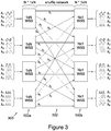
- two WDM reconfigurable optical switches may be combined back-to-back to provide an N x N wavelength selective switch.
- this may be achieved by connecting each output of each WSS array from the first switch to an input of each WSS of the second switch. That is, for example, a first WSS of the first switch has outputs which are connected to an input of each of the WSSs of the second switch (output one to WSS 1 of the second switch, output 2 to WSS 2 of the second switch and so forth); and each of the WSSs of the first switch is connected in this way.
- the optical connections may be made in any convenient manner.
- this shows an embodiment of an N x N wavelength selective switch or optical router 300 comprising first and second WDM reconfigurable optical switches 100a, 100b, each as previously described, connected back-to-back by a set of optical connections 302, to implement a non-blocking WSS router.
- the set of connections 302 may be referred to as a shuffle network ( N 2 x N 2 ), more particularly a static shuffle network, and may be implemented, for example by one or more of: a fibre shuffle network connected to the 1 x N output ports and N x 1 input ports; free space optics; or a planar lightwave circuit, which may include additional functionality, for example channel monitoring for active alignment.
- a commercially available fibre shuffle network may be employed comprising individual single mode fibres laminated to a flexible substrate for mechanical rigidity, typically with the inputs and outputs are separately connectorized.
- each port may support C wavelength channels, where in principle C may be any number greater than 2.
- C may be any number greater than 2.
- channels may be of variable width (wavelength range) so that, for example, a pair of adjacent channels might be combined. In such an arrangement C is variable.
- LCOS liquid crystal on silicon
- WSSs wavelength selective switches
- a 1 ⁇ N WSS has one input port and N output ports and an N ⁇ 1 WSS has N input ports and one output port, and is a 1 ⁇ N WSS used in reverse.
- An LCOS SLM is used by way of example - the designs can also be implemented using a transmissive SLM.
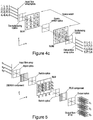
- Figure 4a illustrates the functional optical layout of a generic 1xN WSSs, dispersing WDM wavelength channels across a LCOS phase modulating device, and using gratings to steer the signal beams to specific output fibres.
- the switch comprises:
- the LCOS SLM operates in reflection due to the fact that a silicon chip is used to implement the array of individually addressable electrodes that make spatial phase modulation possible. As a result, the switch is typically folded back on itself.
- the input fibre and output fibre array are in embodiments fabricated as a single component.
- a single grating operates as both the DEMUX and MUX component, as does the input and output switch optics. This is also true for the input and output optics.
- the same optical configuration shown in Fig. 4a can also be used as an Nx1 WSS.
- Nx1 WSS we consider the reversibility of optics. For example, as a 1xN WSS we may route ⁇ 1 and ⁇ 2 from the central input port to output ports 2 and 4 respectively. If we reverse the propagation of light through system so that we have eight input ports and one centrally located output port, both ⁇ 1 from port 2 and ⁇ 2 from port 4 will be routed to the same central output port without having to change the sub-hologram phase patterns. Thus, as long as there is no signal contention (two wavelengths of the same value entering the switch via different input ports), we can implement an Nx1 WSS.
- An LCOS based 1xN WSS may be constructed using anamorphic (cylindrical) switch optics to convert the input signals to elongated beams at the LCOS plane, as illustrated in Fig. 4b .
- the output ports extend along an axis perpendicular to a direction of dispersion.
- the switch design has a sufficient passband, defined as the change in central carrier frequency from its ideal ITU value that results in an increase in insertion loss of 0.5dB, to minimally affect the data being transmitted through the switch. This sets a minimum ratio of unmodulated signal beam radius to sub-hologram width in the direction of wavelength dispersion.
- Such a sub-hologram can steer in both the x and y-directions equally well, with a maximum radial deflection in the xy-plane dependent on the minimum number of pixels per grating period, p min , we allow. As mentioned, in practice we set this value as > 8 pixels in order to maximize sub-hologram diffraction efficiency.
- a circularly symmetric Gaussian beam incident may cover at most 15 pixels at the LCOS SLM plane in both the x and y directions if we are dealing with a 2K LCOS SLM and 80x50GHz signal channels.
- p min 4
- ⁇ SLM 5
- ⁇ i 3
- anamorphic (cylindrical) switch optics that simultaneously image the input fibre beam in the x-axis, and create an elongated beam along the y-axis with a Fourier-transform condition between the SLM plane and the output plane along the same axis.
- a drawback of this approach is that we are unable to steer the beam in the x-direction.
- the switch comprises:
- the switch operates as follows:
- each sub-hologram can steer light in two-dimensions, to prevent signal contention in a WSS, light is only steered in the yz-plane between the two LCOS SLM planes.
- Such a system may be improved by considering the elongated beams at the sub-holograms, to maximize the values of N and M.
- Typical channel spacing's are 100GHz, 50GHz, 37.5HGz, or 25GHz.
- Flex-spectrum also referred to as Flex-grid, is a newer standard that allows for more flexible channel allocation, allowing a higher efficiency in the use of the available spectral bandwidth.
- this specification when we refer to square sub-holograms, we generally (but not exclusively) refer to an unmodulated signal that has a circular Gaussian beam profile at the sub-hologram plane.
- the spectral content of a channel will also increase.
- the width of a sub-hologram will expand in the x-direction to accommodate the wavelength channel.
- FIG. 5 this shows a 1 ⁇ S array of input fibres (denoted S 1 , S 2 , and S 3 in this example), each carrying a set of WDM wavelength channels launch light into the switch.
- the input from each fibre is dealt with separately, and the wavelength channels from a specific input port are spatially de-multiplexed across a unique row of sub-holograms.
- the wavelength channels are then independently routed to a corresponding two dimensional fibre array comprised of S sub-arrays.
- the switch optics are designed to produce circular unmodulated signal beams at the LCOS SLM plane rather than elongated beams using anamorphic optics.
- the output fibre array is arranged as a two-dimensional structure where one can either use an SxN array of separate fibres at the output plane, or S multi-core fibres, each containing N separate fibre cores, as described later.
- a wavefront-modifying or "filter” element may be placed at the common input plane to the objective lenslet, that is at plane P o .
- This filter acts as a "lock” that may then be matched by a suitably modified sub-hologram phase pattern.
- This has the effect of only correcting for the signal beam, and causes the other diffraction orders to couple inefficiently into the output fibres, thereby reducing crosstalk.
- a switch system as described may incorporate a (single) filter a common plane for all output beams on the 1 ⁇ N WSS switch structure.
- the relay system simply images the LCOS SLM plane at plane P o , the implementation reduces to optimizing the output optics and the LCOS SLM hologram pattern.
- Crosstalk from a blazed grating occurs due to quantization of the displayed phase pattern, which can be further exacerbated by the edge effect.
- the edge effect in a LCOS SLM device is a result of pixel fringing fields (the electric field due to the voltage applied to a pixel leaking across to neighbouring pixels) and liquid crystal material effects, and causes errors in the displayed phase profile (we have described techniques to mitigate this in WO2012/110811 ).
- WO 2012/123715 we can suppress crosstalk using an Axicon phase structure.
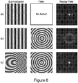
- wavefront encoding based on an Axicon phase element as follows:
- the columns show the phase pattern at the sub-hologram plane, the filter, and the corresponding replay plane.
- the rows show (a) grating and no Axicon, (b) grating and Axicon, and (c) modified grating (grating plus compensating Axicon phase profile) and Axicon.
- the higher and symmetric crosstalk orders of (a) are now spatially dispersed into effectively rings, whilst the signal beam is still focused.
- the calculations assume a sub-hologram of 50x50 pixels with an incident Gaussian beam radius one fifth of the sub-hologram size.
- the grating period is eight pixels, and the Axicon slant angle is 3°.
- a total of 128 phase levels are assumed, and the nematic liquid crystal edge effect is included in the simulation.
- the wavefront modification element may comprise a more general matched spatial filter, for example of the type used in optical correlator technology and optical data encryption.
- the phase profile of the filter may be optimized to diffract light away from the fibre cores unless an inverse phase profile is added to the grating phase profile.
- the common matched spatial filters in a stacked 1 ⁇ N WSS may be implemented using the LCOS SLM, thereby allowing for possible reconfiguration.
- An advantage of this approach is that one can optimize the matched spatial filter phase profile to minimize crosstalk in an arbitrary manner.
- a non-standard Gaussian beam in embodiments a super Gaussian beam, in a wavelength selective switch (WSS) of the type described above.
- WSS wavelength selective switch
- the passband is an important performance parameter for WSS.
- the passband can also be improved by displaying holograms with different diffraction efficiencies for different spectral regions on the SLM.
- this method increases the insertion loss of the switch.
- Figure 7a shows WSS passbands with the standard Gaussian and 3 rd to 6 th order super Gaussian beams with the same value of w SLM .
- the central frequency of these beams is 194000 GHz and ⁇ SLM is 5 for a 50 GHz channel.
- a beam passing through a WSS has a spectral distribution which is a convolution between that of the input signal and the passband (filter function) of the WSS.
- Figure 7b shows the beam profile shapes on the SLM plane which result in the passbands illustrated in Figure 7a .
- the optical signal will go through multiple WSSs.
- the cumulative passband of cascaded WSSs is important.
- the central frequency of the passbands of individual WSSs may be misaligned in a telecoms network.
- An example is illustrated in Figure 9 , where the dashed lines illustrate passbands of three individual WSSs. These passbands are misaligned; the solid line shows the accumulative passband when the three WSSs are cascaded.
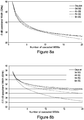
- Figures 10a and 10b show a simulation of this.
- the misalignment of the 50 GHz passband of WSSs follows a normal distribution with a standard deviation of 1 GHz.
- the worst-case cascaded passbands were identified with the respect to the number of cascaded WSSs.
- the results for the -3 dB and -0.5 dB passbands are shown in Figures 10a and 10b respectively. It can be seen that a super Gaussian beam shape on the SLM plane improves the cascaded passband width in a case where multiple WSSs are coupled in series.
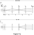
- Figure 11a shows an example of a WSS switch.
- a micro-lens array, L A is used to increase the effective mode field radius of each single mode fibre in the fibre array in order to more closely match the dimension of the optical components and the deflection capabilities of the SLM.
- the plane P o becomes the effective input/output plane of the switch.
- Lens L 1 and Lens L 2 together image the input/output plane to the SLM plane (P SLM ), optionally also with some magnification.
- the (in this example 1-D) linear diffraction grating (P g ) affects the optical propagation along the dispersion axis. More particularly it disperses the C-band wavelengths along the dispersion axis on the SLM.
- the switch may have a 2D output port arrangement, depending on the beam steering capability of the SLM.
- the beam has a Gaussian profile along the dispersion axis on the SLM plane.
- one or more beam-shaping elements can be included in this system to generate a super Gaussian beam profile along the dispersion axis on the SLM plane.
- FIG. 11b One example implementation is illustrated in Figure 11b .
- free-form optics, array L A ' is used to generate a super Gaussian beam profile at the plane P o . This is subsequently imaged to the plane P SLM by L 1 and L 2 .
- the free-form optics only converts the specific wavefront at P o back to the standard Gaussian beam, and thus only this is subsequently coupled into the fibre with high efficiency, resulting in some suppression of crosstalk.
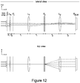
- FIG. 12 Another example implementation is illustrated in Figure 12 .
- a refractive/diffractive optical element, array L FO is inserted immediately after (adjacent to) the fibre (array). Together with the micro-lens array (array L A ), this generates a super Gaussian beam profile at the plane P o , which is subsequently imaged to the plane P SLM by L 1 and L 2 .
- refractive/diffractive optical element only converts the specific wavefront at P o back to the standard Gaussian beam, and thus only this is subsequently coupled into the fibre with high efficiency, resulting in some suppression of crosstalk.
- FIG. 13 A further example implementation is illustrated in Figure 13 .
- the refractive/diffractive optical element (P sg ) is inserted immediately before (adjacent to) the diffractive grating (P g ).
- the refractive/diffractive optical element (P sg ) generates a super Gaussian beam profile at its replay field, which coincides with the SLM plane (P SLM ).
- a computer generated hologram (CGH) algorithms for example Gerchberg-Saxton algorithm or simulated annealing procedure, may be used to design the phase profile of the/an individual refractive/diffractive optical element.
- Figure 14 shows an example phase profile with respect to the beam intensity profile at the plane of the inserted optical element.
- P gsg angle exp i P g + P sg
- P gsg the phase profile of the combined element
- P g the phase profile of the diffractive grating
- P sg the phase profile of the diffractive/refractive optical element responsible for the super Gaussian beam generation.
- any optical defects introduced by the refractive/diffractive optical element may be compensated by the sub-hologram for the beam steering.
- a computer generated hologram procedure may be employed to calculate the relevant hologram.
- a kinoform is a phase (only) hologram (rather than an amplitude hologram).
- WSSs employ kinoform holograms displayed on an SLM.
- a holographic approach where a spatially non-periodic phase pattern is displayed, allows deflection to a 3D volume rather than a 2D plane, and in embodiments we use this for wavefront encoding.
- the pattern displayed on a dynamic hologram is adjusted to ensure optimum coupling of the +1 diffraction order into the desired output port, resulting in defocus of the noise orders.
- Figures 16a and 16b illustrate the idea of wavefront encoding based on defocusing.
- the 2f optical arrangement of Figure 16a comprises an input/output fibre array 1602 comprising, in this example, a single input fibre 1602a and a plurality of output fibres 1602b.
- the array 1602 is positioned at plane F 1 , and the apparatus also comprises a reflective spatial light modulator 1606, and a Fourier transform lens 1604 (as previously described).
- the input signal launched into the system via a central fibre 1602a, is collimated, and is then incident on the SLM 1606 where a quantized phase-only blazed grating is displayed.
- the incident beam is diffracted into a number of orders, the power in each, P m , being dependent on the exact nature of the phase pattern, which are focused at plane Q 1 . Due to the symmetry of this system, planes Q 1 and F 1 coincide, and the focused beams have the same spot profile, though different peak intensities. This can lead to crosstalk, wherein if we aim to direct the +1 order to one of the output fibres, light remaining in other orders may couple into one or more of the other fibres. To address this problem we purposefully move the fibre array back a distance s from plane F 1 to plane F 2 , and compensate for the defocusing effect by adding a lens function to the grating. This can be done, for example, by displaying an off-axis lens. Combining a grating with a lens results in the diffraction orders being focused at different planes.
- FIG 16b shows a schematic illustration of defocused optical beam routing apparatus employing wavefront encoding according to an embodiment of the invention.
- the kinoform incorporates lens power and thus has curved rather than straight "fringes".
- an input beam 1610 from input fibre 1602a is diffracted by reflective LCOS SLM 1606 to provide an output beam 1612.
- Figure 16c shows a simple practical embodiment of optical beam routing apparatus employing wavefront encoding, according to the invention.
- the apparatus of Figure 16c includes a data processor 1660 having a select input 1662 to receive output selection data for selecting one (or more) outputs to which to steer the input beam (or beams).
- Data processor 1660 also provides a drive output 1664 for driving SLM 1606 with selected kinoform data, and non-volatile memory 1666 storing kinoforms for display to i) route the output beam to the selected output(s) and ii) apply a wavefront modification correction for the selected output(s).
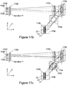
- Figure 17c shows an embodiment of the wavefront encoding technique we describe applied to a WDM switching structure.
- Figure 17b shows a WDM switch where independent, spatially separated, periodic blazed gratings are displayed on the SLM to route light from one input fibre to a number of output fibres.
- the system comprises: A linear single-mode input/output fibre ribbon array 1722; a lenslet array 1728 having the same pitch as the fibre array and lenslets of substantially identical focal lengths; a collimating lens 1730 of focal length f1; a static transmission grating (multiplexer/demultiplexer) 1732 that angularly disperses the WDM wavelengths; a cylindrical lens 1734 of focal length (f1)/2; and a reflective spatial light modulator 1736.
- each wavelength has its own sub-grating 1738 displayed on SLM 1736.
- This is essentially a Fourier-transform based interconnect, where the input/output plane is placed at the front focal plane of a lens, and the SLM placed at the back focal plane.
- Input data 1724 is routed to output 1726; different wavelength components of the input data may be routed to different selected outputs.
- the reason for this mode conversion is to ensure that the beam entering the switch has a divergence to match the SLM beam steering capabilities, the limited dispersion angle of the static de-multiplexing grating, and the requirement to cover a sufficient number of SLM pixels for efficient diffraction.
- the input beam is collimated by the collimating lens, de-multiplexed by the static diffraction grating into a linear spread of wavelengths which are focused by the cylindrical lens into an array of elliptical beams on the SLM ready to acquire an angular deflection.
- beams cover 400 pixels in the y-direction and 5 pixels in the x-direction. Deflection is in the yz plane.
- the beam then retraces its steps, is multiplexed by the diffraction grating and any angular displacement it has achieved at the SLM is converted into a positional displacement at the lenslet array.
- the light is then focused down by a lenslet in front of each fibre to maximize coupling efficiency.
- the system in order to ensure that the light launched into each fibre is normal to that fibre, and that the wavelengths focused onto the SLM plane are normal to the SLM for each wavelength, we arrange the system so that the optics are doubly telecentric.
- the cylindrical lens focuses each wavelength to a beam waist in the x direction, whilst the light remains collimated in the y-direction.
- the system of Figure 17b therefore has similar crosstalk characteristics to the system shown in Figure 17a as the diffraction orders are all focused at the same plane.
- FIG. 17c this shows an example of a WDM switch using wavefront encoding according to an embodiment of the invention, with the aberration introduced by a second cylindrical lens.
- a non-periodic kinoform in this case as an off-axis cylindrical lens of the correct focal length, the target order is no longer astigmatic, and therefore couples efficiently into the target fibre.
- the other diffraction orders of the off-axis cylindrical lens however, further aberrate, and couple inefficiently.
- a cylindrical lens to aberrate the input light and displaying a compensated kinoform, one can reduce crosstalk in the switch.
- Each wavelength has its own separate sub-kinoform (and these may be optimized for optimum performance using the techniques described in our co-pending UK patent application GB1102715.8 ).
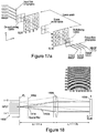
- Figure 18 illustrates similar optical beam routing apparatus to that of Figure 16b , but incorporating a spatial filter 1802. This provides a light block at the location of the zeroth order focus 1614 to attenuate the zeroth order.
- Similar spatial filtering may be incorporated into other embodiments of the invention.
- using this approach can reduce the transient crosstalk that occurs during the change of an interconnection pattern.
- a Fourier-transform can be used to design kinoforms/holograms for beam-steering switches using an iterative algorithm, such as the Gerchberg-Saxton routine when the replay field is located at the Fourier plane of a lens.
- One such algorithm is the fractional Fourier transform. (An alternative calculation approach is to consider the one or more optical outputs as point sources and to propagate waves back from these to define the desired phase and amplitude at a selected plane, until the kinoform/hologram is determined).
- a Fourier transform directly relates an input field to the spatial frequency components making up that field.
- fractional Fourier transform as relating the same input field to an intermediate plane that can be described as comprising a combination of spatial and frequency elements [see, for example, H. M. Ozaktas and D. Mendlovic, "Fractional Fourier optics", J. Opt. Soc. Am. A, 12, pp 743-748 (1995 ); and L. M. Bernardo, "ABCD matrix formalism of fractional Fourier optics", Opt. Eng. 35, pp 732-740 (1996 )].
- Any optical system comprising an input plane, an output plane, and a set of optics in between can be represented using an ABCD matrix (used in ray-tracing and Gaussian beam propagation theory).
- ABCD matrix used in ray-tracing and Gaussian beam propagation theory.
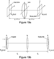
- the Lohmann type I system of Figure 19a was replaced by an equivalent three lens system as shown in Figure 19b .
- the input plane is immediately before the first lens, and the output lens is immediately after the last lens.
- the distance from the first lens to the central lens is f f
- the distance from the central lens is likewise f f .
- the first and last lenses have a focal length of f 1
- the central lens has a focal length of f f .
- FIG 20a shows the switch of Figure 16b unfolded into a transmission system to more clearly relate how the optical system parameters affect the formulation of the fractional Fourier transform.
- the input fiber is positioned at plane P IN
- the output fibers are positioned at planes P R (both equivalent to F 2 in Figure 16b ).
- Lenses L 1 and L 2 are identical, and have a focal length of f.
- z 2 f+s, with s being positive.
- the wavefront incident on ⁇ H is therefore convergent, and the beam focused a distance d o from the lens as shown.
- This scaled focal length and new value of ⁇ takes into account the nature of the non-planar beam incident on the hologram plane, and with these new parameters we can use the equivalent model representation described previously to calculate the replay field of a quantized SLM in a wavefront encoded switch.
- the focal length of the holographic lens, f H required to focus an incident wavefront with radius of curvature - ⁇ H at the replay plane must be such that the wavefront of curvature of the +1 order exiting the SLM is also - ⁇ H . This ensures that the light diffracted from the SLM is optimally focused into the output fibers.
- f H ⁇ 1 / 2 ⁇ H
- a “ping pong” algorithm comprises initialising a phase distribution for the kinoform, for example randomly or based on an initial target replay field, calculating a replay field of the kinoform, modifying an amplitude distribution of the replay field but retaining the phase distribution, converting this modified replay field to an updated kinoform and then repeating the calculating and modifying to converge on a desired target replay field).
- E I (u,v) the replay field
- the plane wavefront which we denote as E in (x,y) to take into account any amplitude profile
- the pixilated LCOS SLM is assumed to display a phase-only hologram represented by a(x,y), where 0 ⁇ (x,y) ⁇ 2 ⁇ .
- the resulting transmitted wavefront, E H (x,y) is the product of these two terms.
- the first lens of Figure 19a , f 1 imparts a quadratic phase curvature on E H (x,y).
- step 3 the central lens, f f performs a Fourier-transform on the wavefront exiting lens f 1 .
- Fractional fast Fourier transform code available from the following web sites: www2.cs.kuleuven.be/ ⁇ nalag/research/software/FRFT/ - for 1D code, and www.ee.bilkent.edy.tr/ ⁇ haidun/fracF.m - for 2D code.
- the SLM comprised a linear array of 400 pixels of pixel size 15 ⁇ m, with the SLM illuminated by a collimated Gaussian replay field of beam radius 2mm at a wavelength of 1550nm.
- the replay position is located -0.75mm from the optical axis, and the phase values were allowed to take any value between 0 and 2 ⁇ .
- FrFFT fractional Fourier transform
- a fractional Fourier transform
- FrFFT[field, 2-a] FrFFT[field, 2-a]
- phase hologram pattern More generally, however, one can calculate a suitable phase hologram pattern based on the transfer function of the optical system.
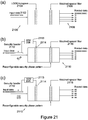
- this shows a generic configuration of an optical router/switch 2100 including a predetermined static matched spatial filter 2106.
- Optical input data 2102 is routed by a sub-hologram phase pattern on LCOS SLM 2104.
- the sub-hologram is optimized to maximize the signal routed to the required output port(s) 2108, and to minimize crosstalk to the non-interconnected output ports.
- the sub-hologram also compensates for the presence of the matched spatial filter 2106.
- Figure 21b shows a generic optical router/switch 2110 including a hardwired security feature. In operation:
- Figure 21c corresponds to Figure 21b but illustrates a case where the header sub-hologram pattern does not match the matched spatial filter pattern. In this case the data does not couple efficiently into any of the output ports.
- the matched spatial filter may be implemented using a LCOS SLM, and may therefore be externally reconfigurable (for example, set by the owner of the network). As a result, the lock phase pattern may be periodically updated, and a new key issued for network users.
- a pixel can have up to 256 distinct phase levels
- the number of optically discrete states (defined as states that produce measurably different insertion loss crosstalk values) is less there are still many different combinations available.
- Preferred embodiments of the system employ an optimization procedure that simultaneously maximizes the LCOS hologram and matched spatial filter for specific security features.
Landscapes
- Engineering & Computer Science (AREA)
- Computer Networks & Wireless Communication (AREA)
- Signal Processing (AREA)
- Optical Modulation, Optical Deflection, Nonlinear Optics, Optical Demodulation, Optical Logic Elements (AREA)
- Diffracting Gratings Or Hologram Optical Elements (AREA)
Claims (15)
- Rekonfigurierbarer optischer wellenlängegemultiplexter (WDM) Schalter (100), wobei der Schalter (100) Folgendes umfasst:mindestens einen optischen Eingangsanschluss (102) zum Empfangen eines optischen WDM-Eingangssignals, welcher eine Vielzahl von Wellenlängenkanälen umfasst;eine Vielzahl von optischen Ausgangsanschlüssen (104);eine rekonfigurierbare holographische Anordnung (108) in einem Strahlengang zwischen dem mindestens einen optischen Eingangsanschluss und der Vielzahl von optischen Ausgangsanschlüssen; undmindestens ein Beugungselement (106) in einem Strahlengang zwischen dem mindestens einen optischen Eingangsanschluss und der rekonfigurierbaren holographischen Anordnung, zum Demultiplexen des optischen WDM-Eingangssignals in eine Vielzahl von demultiplexten optischen Eingangsstrahlkanälen, und zum räumlichen Streuen der demultiplexten optischen Eingangsstrahlkanäle entlang einer ersten Achse (Nx) an der rekonfigurierbaren holographischen Anordnung;wobei die rekonfigurierbare holographische Anordnung eine Anordnung von konfigurierbaren Subhologrammen (112, 112') umfasst, wobei die Anordnung sich entlang der ersten Achse erstreckt, wobei ein Subhologramm konfiguriert ist, um einen demultiplexten optischen Eingangsstrahlkanal auf einen jeweiligen gewählten Anschluss der optischen Ausgangsanschlüsse zu richten; undwobei der Schalter (100) ferner ein oder mehrere optische Strahlprofilierungselemente zum Modifizieren von Quer-Strahlprofilen der demultiplexten optischen Eingangsstrahlkanäle zu modifizierten Strahlprofilen umfasst, wobei ein solches modifiziertes Strahlprofil ein Strahlprofil umfasst, welches ein oder mehrere Merkmale aufweist, gewählt aus einer Gruppe, bestehend aus einem abgeflachten Strahlprofil, einem Strahlprofil mit einer steileren Seite und einem Strahlprofil, welches im Wesentlichen in eine rechteckige Hülle passt, undwobei das eine oder die mehreren optischen Strahlprofilierungselemente konfiguriert sind, um die Quer-Strahlprofile der demultiplexten optischen Eingangs strahlkanäle in einer Weise zu modifizieren, das s eine räumliche Quer-Dimension eines demultiplexten optischen Eingangsstrahlkanals im Wesentlichen mit einer entsprechenden räumlichen Quer-Dimension eines solchen Subhologramms in der rekonfigurierbaren holographischen Anordnung übereinstimmt.
- Rekonfigurierbarer optischer WDM-Schalter nach Anspruch 1, wobei das eine oder die mehreren optischen Strahlprofilierungselemente ein oder mehrere optische Brechungs-/Beugungselemente beinhalten, um die Quer-Strahlprofile der demultiplexten optischen Eingangsstrahlkanäle ohne wesentlichen Strahlenergieverlust zu modifizieren.
- Rekonfigurierbarer optischer WDM-Schalter nach Anspruch 1 oder 2, wobei das eine oder die mehreren optischen Strahlprofilierungselemente konfiguriert sind, um die Quer-Strahlprofil der demultiplexten optischen Eingangsstrahlkanäle abzuflachen.
- Rekonfigurierbarer optischer WDM-Schalter nach einem der Ansprüche 1 bis 3, wobei das mindestens eine Beugungselement ein Quer-Phasenprofil aufweist, welches konfiguriert ist, um eine Strahlform in einer Weise bereitzustellen, dass das Quer-Phasenprofil des mindestens einen Beugungselements Quer-Strahlprofile der demultiplexten optischen Eingangsstrahlkanäle modifiziert, um ein genanntes Strahlprofil abzuflachen.
- Rekonfigurierbarer optischer WDM-Schalter nach einem der Ansprüche 1 bis 4, wobei das eine oder die mehreren optischen Strahlprofilierungselemente eine optische Oberfläche umfassen, welche im Wesentlichen angrenzend an eine Position des mindestens einen Beugungselements befindlich ist, um ein Phasenprofil zu dem mindestens einen Beugungselement hinzuzufügen, um das Strahlprofil abzuflachen.
- Rekonfigurierbarer optischer WDM-Schalter nach einem der Ansprüche 1 bis 5, ferner umfassend Relaisoptiken zwischen dem mindestens einen Beugungselement und einem oder beiden von dem mindestens einen optischen Eingangsanschluss und den optischen Ausgangsanschlüssen; wobei die Relaisoptik die rekonfigurierbare holographische Anordnung in einer Zwischenbildebene abbildet, wobei der Schalter ferner eine Elementarlinsenanordnung zwischen der Zwischenbildebene und einem oder beiden von dem mindestens einen optischen Eingangsanschluss und den optischen Ausgangsanschlüssen umfasst, um den effektiven Eingangs-/Ausgangs-Modenfeldradius jedes Anschlusses zu erhöhen.
- Rekonfigurierbarer optischer WDM-Schalter nach Anspruch 6, wobei das eine oder die mehreren optischen Strahlprofilierungselemente Linsen der Elementarlinsenanordnung enthalten.
- Rekonfigurierbarer optischer WDM-Schalter nach einem der Ansprüche 1 bis 7, wobei das eine oder die mehreren optischen Strahlprofilierungselemente eine Anordnung aus optischen Brechungs-/Beugungselementen umfassen, welche an jeden des mindestens einen optischen Eingangsanschlusses und der optischen Ausgangsanschlüsse angrenzt.
- Rekonfigurierbarer optischer WDM-Schalter nach einem der Ansprüche 1 bis 8, wobei die rekonfigurierbare holographische Anordnung konfiguriert ist, um eine optische Aberration des einen oder der mehreren optischen Strahlprofilierungselemente zu kompensieren.
- Rekonfigurierbarer optischer WDM-Schalter nach einem der Ansprüche 1 bis 9, ferner umfassend ein oder mehrere optische Strahlprofilierungselemente zum Wiederherstellen der abgeflachten Strahlprofile der gerichteten demultiplexten optischen Strahlkanäle zu einem im Wesentlichen originalen Strahlprofil der demultiplexten optischen Eingangsstrahlkanäle.
- Rekonfigurierbarer optischer WDM-Schalter nach Anspruch 10, welcher so konfiguriert ist, dass dasselbe eine oder dieselben mehreren optischen Strahlprofilierungselemente die Strahlprofile gleichermaßen modifizieren und wiederherstellen.
- Verfahren zum Routing eines wellenlängengemultiplexten, WDM, Signals, welches eine Vielzahl von Wellenlängenkanälen umfasst, wobei das Verfahren Folgendes umfasst:Empfangen in mindestens einem optischen Eingangsanschluss eines optischen WDM-Eingangssignals, welches eine Vielzahl von Wellenlängenkanälen umfasst;Streuen des WDM-Eingangssignals in eine Vielzahl von demultiplexten Strahlen, welche jeweils einen WDM-Kanal umfassen;Bereitstellen der demultiplexten Strahlen an eine Gruppe von jeweiligen Strahllenkungselementen, jeweils zum Lenken eines jeweiligen WDM-Kanals;Erzeugen einer Vielzahl von gelenkten Strahlen aus den Strahllenkungselementen, einen für jeden WDM-Kanal; undRouting der gelenkten Strahlen in ausgewählte Strahlenausgänge unter Verwendung einer rekonfigurierbaren holographischen Anordnung, umfassend eine Anordnung von konfigurierbaren Subhologrammen in einem Strahlengang zwischen dem mindestens einen optischen Eingangsanschluss und einer Vielzahl von optischen Ausgangsanschlüssen, wobei ein Subhologramm einen demultiplexten optischen Eingangskanal auf einen jeweiligen ausgewählten der optischen Ausgangsanschlüsse richtet;wobei das Verfahren ferner Modifizieren von Quer-Strahlprofilen der demultiplexten Strahlen zu modifizierten Strahlprofilen unter Verwendung eines oder mehrerer optischer Strahlprofilierungselemente umfasst, wobei ein solches modifiziertes Strahlprofil ein Strahlprofil umfasst, welches ein oder mehrere Merkmale aufweist, gewählt aus einer Gruppe, bestehend aus: einem abgeflachten Strahlprofil, einem Strahlprofil mit einer steileren Seite und einem Strahlprofil, welches im Wesentlichen in eine rechteckige Hülle passt, undwobei das eine oder die mehreren optischen Strahlprofilierungselemente konfiguriert sind, um die Quer-Strahlprofile der demultiplexten optischen Eingangs strahlkanäle in einer Weise zu modifizieren, dass eine räumliche Quer-Dimension eines demultiplexten optischen Eingangsstrahlkanals im Wesentlichen mit einer entsprechenden räumlichen Quer-Dimension eines solchen Subhologramms in der rekonfigurierbaren holographischen Anordnung übereinstimmt.
- Verfahren nach Anspruch 12, ferner umfassend Wiederherstellen der Strahlprofile vor dem Ausgeben der gelenkten Strahlen.
- Verfahren nach Anspruch 12 oder 13, wobei das Modifizieren Umwandeln der Strahlprofile in abgeflachte Strahlprofile umfasst.
- Verfahren nach Anspruch 12, 13 oder 14, ferner umfassend Bereitstellen der Gruppe von jeweiligen Strahllenkungselementen durch Anzeigen einer Gruppe von Subhologrammen an einem räumlichen Lichtmodulator (SLM); und Zuordnen einer oder zweier rechtwinkliger räumlicher Quer-Dimensionen eines demultiplexten Strahls zu einer oder zwei entsprechenden rechtwinkligen räumlichen Quer-Dimensionen eines solchen an dem SLM angezeigten Subhologramms, wobei optionsweise das Modifizieren der Quer-Strahlprofile ohne wesentliche Dämpfung der Strahlen erfolgt.
Applications Claiming Priority (2)
| Application Number | Priority Date | Filing Date | Title |
|---|---|---|---|
| GBGB1516870.1A GB201516870D0 (en) | 2015-09-23 | 2015-09-23 | Optical systems |
| PCT/GB2016/052913 WO2017051158A1 (en) | 2015-09-23 | 2016-09-19 | Optical systems |
Publications (2)
| Publication Number | Publication Date |
|---|---|
| EP3354040A1 EP3354040A1 (de) | 2018-08-01 |
| EP3354040B1 true EP3354040B1 (de) | 2020-11-25 |
Family
ID=54544703
Family Applications (1)
| Application Number | Title | Priority Date | Filing Date |
|---|---|---|---|
| EP16770791.8A Active EP3354040B1 (de) | 2015-09-23 | 2016-09-19 | Optische systeme |
Country Status (5)
| Country | Link |
|---|---|
| US (1) | US10587936B2 (de) |
| EP (1) | EP3354040B1 (de) |
| CN (1) | CN108353216B (de) |
| GB (1) | GB201516870D0 (de) |
| WO (1) | WO2017051158A1 (de) |
Families Citing this family (25)
| Publication number | Priority date | Publication date | Assignee | Title |
|---|---|---|---|---|
| US20170248793A1 (en) * | 2016-02-29 | 2017-08-31 | Universal Laser Systems, Inc. | Laser processing system with modified beam energy distribution |
| WO2017196995A1 (en) * | 2016-05-11 | 2017-11-16 | The Regents Of The University Of California | Method and system for pixel super-resolution of multiplexed holographic color images |
| US11838101B2 (en) * | 2018-01-26 | 2023-12-05 | Ciena Corporation | Upgradeable colorless, directionless, and contentionless optical architectures |
| CN110389451B (zh) * | 2018-04-19 | 2022-04-22 | 华为技术有限公司 | 一种光交换装置 |
| WO2020093200A1 (zh) * | 2018-11-05 | 2020-05-14 | 东莞理工学院 | 基于几何光学变换的oam信道提取与添加系统及方法 |
| US20200257066A1 (en) * | 2019-02-11 | 2020-08-13 | Hewlett Packard Enterprise Development Lp | Optical interconnect topology |
| CN111025876B (zh) * | 2019-11-08 | 2021-09-28 | 桂林电子科技大学 | 基于压电陶瓷的透射式相位显微成像测量系统 |
| US10862610B1 (en) | 2019-11-11 | 2020-12-08 | X Development Llc | Multi-channel integrated photonic wavelength demultiplexer |
| US11187854B2 (en) * | 2019-11-15 | 2021-11-30 | X Development Llc | Two-channel integrated photonic wavelength demultiplexer |
| CN113156585B (zh) * | 2020-01-23 | 2025-11-14 | 华为技术有限公司 | 一种波长选择开关wss |
| CN113296191A (zh) * | 2020-02-21 | 2021-08-24 | 华为技术有限公司 | 一种光交换装置、重定向方法以及可重构光分插复用器 |
| US11287585B2 (en) * | 2020-03-11 | 2022-03-29 | Nubis Communications, Inc. | Optical fiber-to-chip interconnection |
| US11448829B2 (en) | 2020-05-12 | 2022-09-20 | Lumentum Operations Llc | M×N wavelength selective switch with compressed port spacing |
| KR102612045B1 (ko) | 2020-11-02 | 2023-12-12 | 한국전자통신연구원 | 디지털 홀로그램 구현 장치의 동작 방법 |
| CN112882369B (zh) * | 2021-02-09 | 2021-12-21 | 北京理工大学 | 基于级联超颖表面全息术的光学秘密共享方法 |
| US12461321B2 (en) | 2021-03-11 | 2025-11-04 | Nubis Communications, Inc. | Optical fiber-to-chip interconnection |
| US11982848B2 (en) | 2021-03-11 | 2024-05-14 | Nubis Communications, Inc. | Optical fiber-to-chip interconnection |
| CN115085815A (zh) * | 2021-03-15 | 2022-09-20 | 华为技术有限公司 | 波长选择交换装置以及相关方法 |
| EP4252826B1 (de) | 2021-10-11 | 2026-02-25 | Magenta Medical Ltd. | Ventrikuläre hilfsvorrichtung |
| CN114185175B (zh) * | 2021-11-23 | 2024-05-17 | 西安中科微星光电科技有限公司 | 一种激光光束整形装置及方法 |
| CN114200328B (zh) * | 2022-01-20 | 2022-09-30 | 中国科学技术大学 | 一种非高斯Lévy噪声下的锂离子电池SOC估计方法 |
| CN117111220A (zh) * | 2022-05-05 | 2023-11-24 | 武汉光迅科技股份有限公司 | 一种抑制波长选择开关瞬态串扰的方法和装置 |
| JP2025530821A (ja) | 2022-09-14 | 2025-09-17 | マジェンタ・メディカル・リミテッド | シャフトと駆動ケーブルとの連結 |
| CN118018883A (zh) * | 2022-11-09 | 2024-05-10 | 华为技术有限公司 | 波长通道分配方法、通道分配设备及通道分配系统 |
| US20250076638A1 (en) * | 2023-09-06 | 2025-03-06 | Lumentum Operations Llc | Multi-bounce optical beam steering |
Family Cites Families (13)
| Publication number | Priority date | Publication date | Assignee | Title |
|---|---|---|---|---|
| US6654183B2 (en) * | 1999-12-15 | 2003-11-25 | International Business Machines Corporation | System for converting optical beams to collimated flat-top beams |
| US7092594B2 (en) * | 2003-03-31 | 2006-08-15 | Fujitsu Limited | Wavelength selector switch |
| US7397980B2 (en) | 2004-06-14 | 2008-07-08 | Optium Australia Pty Limited | Dual-source optical wavelength processor |
| US7756368B2 (en) * | 2005-04-11 | 2010-07-13 | Capella Photonics, Inc. | Flex spectrum WSS |
| US7200299B1 (en) * | 2006-03-23 | 2007-04-03 | Lucent Technologies Inc. | Adding and dropping wavelength-channels |
| CN100478720C (zh) * | 2006-06-23 | 2009-04-15 | 北京大学 | 用平行光纤解决obs中竞争的链路结构及波长分配方法 |
| WO2010084317A1 (en) * | 2009-01-21 | 2010-07-29 | The University Of Dundee | Novel photonic devices based on conical refraction |
| CN102804009A (zh) * | 2009-10-22 | 2012-11-28 | 耶路撒冷希伯来大学伊森姆研究发展公司 | 用于切换光通道的方法和系统 |
| GB201104174D0 (en) | 2011-03-11 | 2011-04-27 | Bhp Generation Ltd | An improved steam engine |
| GB201104235D0 (en) * | 2011-03-14 | 2011-04-27 | Cambridge Entpr Ltd | Optical beam routing apparatus and methods |
| US8867917B2 (en) | 2011-06-27 | 2014-10-21 | Finisar Corporation | Optical wavelength selective switch calibration system |
| WO2013038713A1 (ja) * | 2011-09-16 | 2013-03-21 | 日本電信電話株式会社 | 光スイッチ |
| US10211587B2 (en) * | 2015-03-31 | 2019-02-19 | Versitech Limited | Spatial chirped cavity for temporally stretching/compressing optical pulses |
-
2015
- 2015-09-23 GB GBGB1516870.1A patent/GB201516870D0/en not_active Ceased
-
2016
- 2016-09-19 US US15/762,179 patent/US10587936B2/en active Active
- 2016-09-19 EP EP16770791.8A patent/EP3354040B1/de active Active
- 2016-09-19 WO PCT/GB2016/052913 patent/WO2017051158A1/en not_active Ceased
- 2016-09-19 CN CN201680055877.8A patent/CN108353216B/zh active Active
Non-Patent Citations (1)
| Title |
|---|
| None * |
Also Published As
| Publication number | Publication date |
|---|---|
| WO2017051158A1 (en) | 2017-03-30 |
| US20180288504A1 (en) | 2018-10-04 |
| CN108353216B (zh) | 2021-12-10 |
| GB201516870D0 (en) | 2015-11-04 |
| US10587936B2 (en) | 2020-03-10 |
| EP3354040A1 (de) | 2018-08-01 |
| CN108353216A (zh) | 2018-07-31 |
Similar Documents
| Publication | Publication Date | Title |
|---|---|---|
| US10587936B2 (en) | Optical systems | |
| US10700804B2 (en) | Optical switching systems | |
| US10996399B2 (en) | Space-division multiplexed reconfigurable, wavelength selective switch | |
| US9930431B2 (en) | Optical beam routing apparatus and methods | |
| US20130272650A1 (en) | Wavelength cross connect device | |
| CN104730644B (zh) | 一种基于复合硅基液晶的m×n端口roadm及其控制方法 | |
| US11418861B2 (en) | Optical switching unit | |
| CN111221081B (zh) | 一种基于LCoS的波长选择开关 | |
| CN107976748B (zh) | 基于偏振分束双衍射光栅的多端口波长选择开关及其方法 | |
| Miles et al. | 7× 7 DMD-based diffractive fiber switch at 1550 nm | |
| US20250284065A1 (en) | Optical switch utilizing optical beam steering | |
| US20250291120A1 (en) | Optical Switch Utilising Gap Optics | |
| Yang et al. | Stacked wavelength selective switch design for low-cost CDC ROADMs | |
| GB2612718A (en) | Optical switch utilising gap optics | |
| GB2612717A (en) | Optical switch utilising optical beam steering | |
| Rodrigo Martín Romo | First-order optical systems in information processing and optronic devices | |
| CN119511461A (zh) | 一种波长选择开关及节点装置 |
Legal Events
| Date | Code | Title | Description |
|---|---|---|---|
| STAA | Information on the status of an ep patent application or granted ep patent |
Free format text: STATUS: THE INTERNATIONAL PUBLICATION HAS BEEN MADE |
|
| PUAI | Public reference made under article 153(3) epc to a published international application that has entered the european phase |
Free format text: ORIGINAL CODE: 0009012 |
|
| STAA | Information on the status of an ep patent application or granted ep patent |
Free format text: STATUS: REQUEST FOR EXAMINATION WAS MADE |
|
| 17P | Request for examination filed |
Effective date: 20180222 |
|
| AK | Designated contracting states |
Kind code of ref document: A1 Designated state(s): AL AT BE BG CH CY CZ DE DK EE ES FI FR GB GR HR HU IE IS IT LI LT LU LV MC MK MT NL NO PL PT RO RS SE SI SK SM TR |
|
| AX | Request for extension of the european patent |
Extension state: BA ME |
|
| DAV | Request for validation of the european patent (deleted) | ||
| DAX | Request for extension of the european patent (deleted) | ||
| STAA | Information on the status of an ep patent application or granted ep patent |
Free format text: STATUS: EXAMINATION IS IN PROGRESS |
|
| 17Q | First examination report despatched |
Effective date: 20191210 |
|
| GRAP | Despatch of communication of intention to grant a patent |
Free format text: ORIGINAL CODE: EPIDOSNIGR1 |
|
| STAA | Information on the status of an ep patent application or granted ep patent |
Free format text: STATUS: GRANT OF PATENT IS INTENDED |
|
| INTG | Intention to grant announced |
Effective date: 20200612 |
|
| GRAS | Grant fee paid |
Free format text: ORIGINAL CODE: EPIDOSNIGR3 |
|
| GRAA | (expected) grant |
Free format text: ORIGINAL CODE: 0009210 |
|
| STAA | Information on the status of an ep patent application or granted ep patent |
Free format text: STATUS: THE PATENT HAS BEEN GRANTED |
|
| AK | Designated contracting states |
Kind code of ref document: B1 Designated state(s): AL AT BE BG CH CY CZ DE DK EE ES FI FR GB GR HR HU IE IS IT LI LT LU LV MC MK MT NL NO PL PT RO RS SE SI SK SM TR |
|
| REG | Reference to a national code |
Ref country code: GB Ref legal event code: FG4D |
|
| REG | Reference to a national code |
Ref country code: CH Ref legal event code: EP |
|
| REG | Reference to a national code |
Ref country code: AT Ref legal event code: REF Ref document number: 1339675 Country of ref document: AT Kind code of ref document: T Effective date: 20201215 |
|
| REG | Reference to a national code |
Ref country code: DE Ref legal event code: R096 Ref document number: 602016048620 Country of ref document: DE |
|
| REG | Reference to a national code |
Ref country code: IE Ref legal event code: FG4D |
|
| REG | Reference to a national code |
Ref country code: AT Ref legal event code: MK05 Ref document number: 1339675 Country of ref document: AT Kind code of ref document: T Effective date: 20201125 |
|
| REG | Reference to a national code |
Ref country code: NL Ref legal event code: MP Effective date: 20201125 |
|
| PG25 | Lapsed in a contracting state [announced via postgrant information from national office to epo] |
Ref country code: NO Free format text: LAPSE BECAUSE OF FAILURE TO SUBMIT A TRANSLATION OF THE DESCRIPTION OR TO PAY THE FEE WITHIN THE PRESCRIBED TIME-LIMIT Effective date: 20210225 Ref country code: RS Free format text: LAPSE BECAUSE OF FAILURE TO SUBMIT A TRANSLATION OF THE DESCRIPTION OR TO PAY THE FEE WITHIN THE PRESCRIBED TIME-LIMIT Effective date: 20201125 Ref country code: PT Free format text: LAPSE BECAUSE OF FAILURE TO SUBMIT A TRANSLATION OF THE DESCRIPTION OR TO PAY THE FEE WITHIN THE PRESCRIBED TIME-LIMIT Effective date: 20210325 Ref country code: GR Free format text: LAPSE BECAUSE OF FAILURE TO SUBMIT A TRANSLATION OF THE DESCRIPTION OR TO PAY THE FEE WITHIN THE PRESCRIBED TIME-LIMIT Effective date: 20210226 Ref country code: FI Free format text: LAPSE BECAUSE OF FAILURE TO SUBMIT A TRANSLATION OF THE DESCRIPTION OR TO PAY THE FEE WITHIN THE PRESCRIBED TIME-LIMIT Effective date: 20201125 |
|
| PG25 | Lapsed in a contracting state [announced via postgrant information from national office to epo] |
Ref country code: BG Free format text: LAPSE BECAUSE OF FAILURE TO SUBMIT A TRANSLATION OF THE DESCRIPTION OR TO PAY THE FEE WITHIN THE PRESCRIBED TIME-LIMIT Effective date: 20210225 Ref country code: IS Free format text: LAPSE BECAUSE OF FAILURE TO SUBMIT A TRANSLATION OF THE DESCRIPTION OR TO PAY THE FEE WITHIN THE PRESCRIBED TIME-LIMIT Effective date: 20210325 Ref country code: LV Free format text: LAPSE BECAUSE OF FAILURE TO SUBMIT A TRANSLATION OF THE DESCRIPTION OR TO PAY THE FEE WITHIN THE PRESCRIBED TIME-LIMIT Effective date: 20201125 Ref country code: PL Free format text: LAPSE BECAUSE OF FAILURE TO SUBMIT A TRANSLATION OF THE DESCRIPTION OR TO PAY THE FEE WITHIN THE PRESCRIBED TIME-LIMIT Effective date: 20201125 Ref country code: AT Free format text: LAPSE BECAUSE OF FAILURE TO SUBMIT A TRANSLATION OF THE DESCRIPTION OR TO PAY THE FEE WITHIN THE PRESCRIBED TIME-LIMIT Effective date: 20201125 Ref country code: SE Free format text: LAPSE BECAUSE OF FAILURE TO SUBMIT A TRANSLATION OF THE DESCRIPTION OR TO PAY THE FEE WITHIN THE PRESCRIBED TIME-LIMIT Effective date: 20201125 |
|
| REG | Reference to a national code |
Ref country code: LT Ref legal event code: MG9D |
|
| PG25 | Lapsed in a contracting state [announced via postgrant information from national office to epo] |
Ref country code: HR Free format text: LAPSE BECAUSE OF FAILURE TO SUBMIT A TRANSLATION OF THE DESCRIPTION OR TO PAY THE FEE WITHIN THE PRESCRIBED TIME-LIMIT Effective date: 20201125 |
|
| PG25 | Lapsed in a contracting state [announced via postgrant information from national office to epo] |
Ref country code: SK Free format text: LAPSE BECAUSE OF FAILURE TO SUBMIT A TRANSLATION OF THE DESCRIPTION OR TO PAY THE FEE WITHIN THE PRESCRIBED TIME-LIMIT Effective date: 20201125 Ref country code: RO Free format text: LAPSE BECAUSE OF FAILURE TO SUBMIT A TRANSLATION OF THE DESCRIPTION OR TO PAY THE FEE WITHIN THE PRESCRIBED TIME-LIMIT Effective date: 20201125 Ref country code: SM Free format text: LAPSE BECAUSE OF FAILURE TO SUBMIT A TRANSLATION OF THE DESCRIPTION OR TO PAY THE FEE WITHIN THE PRESCRIBED TIME-LIMIT Effective date: 20201125 Ref country code: LT Free format text: LAPSE BECAUSE OF FAILURE TO SUBMIT A TRANSLATION OF THE DESCRIPTION OR TO PAY THE FEE WITHIN THE PRESCRIBED TIME-LIMIT Effective date: 20201125 Ref country code: CZ Free format text: LAPSE BECAUSE OF FAILURE TO SUBMIT A TRANSLATION OF THE DESCRIPTION OR TO PAY THE FEE WITHIN THE PRESCRIBED TIME-LIMIT Effective date: 20201125 Ref country code: EE Free format text: LAPSE BECAUSE OF FAILURE TO SUBMIT A TRANSLATION OF THE DESCRIPTION OR TO PAY THE FEE WITHIN THE PRESCRIBED TIME-LIMIT Effective date: 20201125 |
|
| REG | Reference to a national code |
Ref country code: DE Ref legal event code: R097 Ref document number: 602016048620 Country of ref document: DE |
|
| PG25 | Lapsed in a contracting state [announced via postgrant information from national office to epo] |
Ref country code: DK Free format text: LAPSE BECAUSE OF FAILURE TO SUBMIT A TRANSLATION OF THE DESCRIPTION OR TO PAY THE FEE WITHIN THE PRESCRIBED TIME-LIMIT Effective date: 20201125 |
|
| PLBE | No opposition filed within time limit |
Free format text: ORIGINAL CODE: 0009261 |
|
| STAA | Information on the status of an ep patent application or granted ep patent |
Free format text: STATUS: NO OPPOSITION FILED WITHIN TIME LIMIT |
|
| REG | Reference to a national code |
Ref country code: DE Ref legal event code: R081 Ref document number: 602016048620 Country of ref document: DE Owner name: HUBER+SUHNER POLATIS LIMITED, CAMBRIDGE, GB Free format text: FORMER OWNER: ROADMAP SYSTEMS LTD, CAMBRIDGE, CAMBRIDGESHIRE, GB |
|
| PG25 | Lapsed in a contracting state [announced via postgrant information from national office to epo] |
Ref country code: NL Free format text: LAPSE BECAUSE OF FAILURE TO SUBMIT A TRANSLATION OF THE DESCRIPTION OR TO PAY THE FEE WITHIN THE PRESCRIBED TIME-LIMIT Effective date: 20201125 Ref country code: IT Free format text: LAPSE BECAUSE OF FAILURE TO SUBMIT A TRANSLATION OF THE DESCRIPTION OR TO PAY THE FEE WITHIN THE PRESCRIBED TIME-LIMIT Effective date: 20201125 Ref country code: AL Free format text: LAPSE BECAUSE OF FAILURE TO SUBMIT A TRANSLATION OF THE DESCRIPTION OR TO PAY THE FEE WITHIN THE PRESCRIBED TIME-LIMIT Effective date: 20201125 |
|
| 26N | No opposition filed |
Effective date: 20210826 |
|
| PG25 | Lapsed in a contracting state [announced via postgrant information from national office to epo] |
Ref country code: SI Free format text: LAPSE BECAUSE OF FAILURE TO SUBMIT A TRANSLATION OF THE DESCRIPTION OR TO PAY THE FEE WITHIN THE PRESCRIBED TIME-LIMIT Effective date: 20201125 |
|
| PG25 | Lapsed in a contracting state [announced via postgrant information from national office to epo] |
Ref country code: ES Free format text: LAPSE BECAUSE OF FAILURE TO SUBMIT A TRANSLATION OF THE DESCRIPTION OR TO PAY THE FEE WITHIN THE PRESCRIBED TIME-LIMIT Effective date: 20201125 |
|
| REG | Reference to a national code |
Ref country code: GB Ref legal event code: 732E Free format text: REGISTERED BETWEEN 20220317 AND 20220323 |
|
| REG | Reference to a national code |
Ref country code: CH Ref legal event code: PL |
|
| REG | Reference to a national code |
Ref country code: BE Ref legal event code: MM Effective date: 20210930 |
|
| PG25 | Lapsed in a contracting state [announced via postgrant information from national office to epo] |
Ref country code: IS Free format text: LAPSE BECAUSE OF FAILURE TO SUBMIT A TRANSLATION OF THE DESCRIPTION OR TO PAY THE FEE WITHIN THE PRESCRIBED TIME-LIMIT Effective date: 20210325 Ref country code: MC Free format text: LAPSE BECAUSE OF FAILURE TO SUBMIT A TRANSLATION OF THE DESCRIPTION OR TO PAY THE FEE WITHIN THE PRESCRIBED TIME-LIMIT Effective date: 20201125 |
|
| PG25 | Lapsed in a contracting state [announced via postgrant information from national office to epo] |
Ref country code: LU Free format text: LAPSE BECAUSE OF NON-PAYMENT OF DUE FEES Effective date: 20210919 Ref country code: IE Free format text: LAPSE BECAUSE OF NON-PAYMENT OF DUE FEES Effective date: 20210919 Ref country code: BE Free format text: LAPSE BECAUSE OF NON-PAYMENT OF DUE FEES Effective date: 20210930 |
|
| PG25 | Lapsed in a contracting state [announced via postgrant information from national office to epo] |
Ref country code: LI Free format text: LAPSE BECAUSE OF NON-PAYMENT OF DUE FEES Effective date: 20210930 Ref country code: CH Free format text: LAPSE BECAUSE OF NON-PAYMENT OF DUE FEES Effective date: 20210930 |
|
| PG25 | Lapsed in a contracting state [announced via postgrant information from national office to epo] |
Ref country code: HU Free format text: LAPSE BECAUSE OF FAILURE TO SUBMIT A TRANSLATION OF THE DESCRIPTION OR TO PAY THE FEE WITHIN THE PRESCRIBED TIME-LIMIT; INVALID AB INITIO Effective date: 20160919 |
|
| PG25 | Lapsed in a contracting state [announced via postgrant information from national office to epo] |
Ref country code: CY Free format text: LAPSE BECAUSE OF FAILURE TO SUBMIT A TRANSLATION OF THE DESCRIPTION OR TO PAY THE FEE WITHIN THE PRESCRIBED TIME-LIMIT Effective date: 20201125 |
|
| P01 | Opt-out of the competence of the unified patent court (upc) registered |
Effective date: 20230530 |
|
| PG25 | Lapsed in a contracting state [announced via postgrant information from national office to epo] |
Ref country code: MK Free format text: LAPSE BECAUSE OF FAILURE TO SUBMIT A TRANSLATION OF THE DESCRIPTION OR TO PAY THE FEE WITHIN THE PRESCRIBED TIME-LIMIT Effective date: 20201125 |
|
| PG25 | Lapsed in a contracting state [announced via postgrant information from national office to epo] |
Ref country code: TR Free format text: LAPSE BECAUSE OF FAILURE TO SUBMIT A TRANSLATION OF THE DESCRIPTION OR TO PAY THE FEE WITHIN THE PRESCRIBED TIME-LIMIT Effective date: 20201125 |
|
| PG25 | Lapsed in a contracting state [announced via postgrant information from national office to epo] |
Ref country code: MT Free format text: LAPSE BECAUSE OF FAILURE TO SUBMIT A TRANSLATION OF THE DESCRIPTION OR TO PAY THE FEE WITHIN THE PRESCRIBED TIME-LIMIT Effective date: 20201125 |
|
| PGFP | Annual fee paid to national office [announced via postgrant information from national office to epo] |
Ref country code: DE Payment date: 20250929 Year of fee payment: 10 |
|
| PGFP | Annual fee paid to national office [announced via postgrant information from national office to epo] |
Ref country code: GB Payment date: 20250929 Year of fee payment: 10 |
|
| PGFP | Annual fee paid to national office [announced via postgrant information from national office to epo] |
Ref country code: FR Payment date: 20250925 Year of fee payment: 10 |