EP3353885B1 - Procédé de fonctionnement d'un convertisseur de courant modulaire à multiples niveaux, convertisseur de courant modulaire à multiples niveaux ainsi que programme d'ordinateur - Google Patents
Procédé de fonctionnement d'un convertisseur de courant modulaire à multiples niveaux, convertisseur de courant modulaire à multiples niveaux ainsi que programme d'ordinateur Download PDFInfo
- Publication number
- EP3353885B1 EP3353885B1 EP16770497.2A EP16770497A EP3353885B1 EP 3353885 B1 EP3353885 B1 EP 3353885B1 EP 16770497 A EP16770497 A EP 16770497A EP 3353885 B1 EP3353885 B1 EP 3353885B1
- Authority
- EP
- European Patent Office
- Prior art keywords
- converter
- voltage
- output
- bridge
- modulation
- Prior art date
- Legal status (The legal status is an assumption and is not a legal conclusion. Google has not performed a legal analysis and makes no representation as to the accuracy of the status listed.)
- Active
Links
- 238000000034 method Methods 0.000 title claims description 25
- 238000004590 computer program Methods 0.000 title claims description 6
- 239000004065 semiconductor Substances 0.000 claims description 27
- 239000003990 capacitor Substances 0.000 claims description 19
- 230000001105 regulatory effect Effects 0.000 claims description 11
- 230000002123 temporal effect Effects 0.000 claims description 6
- 230000001276 controlling effect Effects 0.000 claims description 4
- 238000005070 sampling Methods 0.000 claims description 3
- 238000011161 development Methods 0.000 description 5
- 238000010586 diagram Methods 0.000 description 5
- 230000000630 rising effect Effects 0.000 description 4
- 230000000694 effects Effects 0.000 description 2
- 210000000245 forearm Anatomy 0.000 description 2
- 238000009413 insulation Methods 0.000 description 2
- 239000011159 matrix material Substances 0.000 description 2
- 230000006978 adaptation Effects 0.000 description 1
- 238000013459 approach Methods 0.000 description 1
- 238000010276 construction Methods 0.000 description 1
- 238000005516 engineering process Methods 0.000 description 1
- 238000011835 investigation Methods 0.000 description 1
- 238000002955 isolation Methods 0.000 description 1
- 238000011017 operating method Methods 0.000 description 1
- 230000010363 phase shift Effects 0.000 description 1
- 230000000087 stabilizing effect Effects 0.000 description 1
Images


Classifications
-
- H—ELECTRICITY
- H02—GENERATION; CONVERSION OR DISTRIBUTION OF ELECTRIC POWER
- H02M—APPARATUS FOR CONVERSION BETWEEN AC AND AC, BETWEEN AC AND DC, OR BETWEEN DC AND DC, AND FOR USE WITH MAINS OR SIMILAR POWER SUPPLY SYSTEMS; CONVERSION OF DC OR AC INPUT POWER INTO SURGE OUTPUT POWER; CONTROL OR REGULATION THEREOF
- H02M7/00—Conversion of ac power input into dc power output; Conversion of dc power input into ac power output
- H02M7/42—Conversion of dc power input into ac power output without possibility of reversal
- H02M7/44—Conversion of dc power input into ac power output without possibility of reversal by static converters
- H02M7/48—Conversion of dc power input into ac power output without possibility of reversal by static converters using discharge tubes with control electrode or semiconductor devices with control electrode
- H02M7/483—Converters with outputs that each can have more than two voltages levels
- H02M7/4835—Converters with outputs that each can have more than two voltages levels comprising two or more cells, each including a switchable capacitor, the capacitors having a nominal charge voltage which corresponds to a given fraction of the input voltage, and the capacitors being selectively connected in series to determine the instantaneous output voltage
-
- H—ELECTRICITY
- H02—GENERATION; CONVERSION OR DISTRIBUTION OF ELECTRIC POWER
- H02M—APPARATUS FOR CONVERSION BETWEEN AC AND AC, BETWEEN AC AND DC, OR BETWEEN DC AND DC, AND FOR USE WITH MAINS OR SIMILAR POWER SUPPLY SYSTEMS; CONVERSION OF DC OR AC INPUT POWER INTO SURGE OUTPUT POWER; CONTROL OR REGULATION THEREOF
- H02M7/00—Conversion of ac power input into dc power output; Conversion of dc power input into ac power output
- H02M7/42—Conversion of dc power input into ac power output without possibility of reversal
- H02M7/44—Conversion of dc power input into ac power output without possibility of reversal by static converters
- H02M7/48—Conversion of dc power input into ac power output without possibility of reversal by static converters using discharge tubes with control electrode or semiconductor devices with control electrode
- H02M7/483—Converters with outputs that each can have more than two voltages levels
- H02M7/49—Combination of the output voltage waveforms of a plurality of converters
-
- H—ELECTRICITY
- H02—GENERATION; CONVERSION OR DISTRIBUTION OF ELECTRIC POWER
- H02M—APPARATUS FOR CONVERSION BETWEEN AC AND AC, BETWEEN AC AND DC, OR BETWEEN DC AND DC, AND FOR USE WITH MAINS OR SIMILAR POWER SUPPLY SYSTEMS; CONVERSION OF DC OR AC INPUT POWER INTO SURGE OUTPUT POWER; CONTROL OR REGULATION THEREOF
- H02M1/00—Details of apparatus for conversion
- H02M1/0003—Details of control, feedback or regulation circuits
- H02M1/0029—Circuits or arrangements for limiting the slope of switching signals, e.g. slew rate
Definitions
- the invention relates to a method for operating a modular multilevel converter which has several converter branches, in each of which series connections of bridge modules are arranged, the bridge modules each having a bridge circuit in the form of a half bridge or a full bridge made of power semiconductors and at least one capacitor that can be switched via the bridge circuit have, wherein the method provides an output AC voltage on an output side of the converter.
- the invention also relates to a modular multilevel converter designed in this way and to a computer program with program code means, set up to carry out a method of the aforementioned type.
- the invention lies in the field of power electronics and, in particular, power converter technology.
- a class of power converters with a suitability for particularly high voltages using commercially available power semiconductors is the class of modular multilevel power converters.
- the principle consists in adding modules consisting of a half bridge or a full bridge of switchable power semiconductors and a usually relatively large capacitor use.
- the required reverse voltage of the power semiconductors is defined by the maximum operating voltage of the capacitor.
- the modules, also called bridge modules are connected in series on the output side.
- the respective Capacitor voltage of the bridge module or a short circuit can be switched, with full bridge modules also the negative capacitor voltage.
- Modular multilevel converters and their operation are, for example, in the publications " Low output frequency operation of the modular multi-level converter "in 2010 IEEE Energy Conversion Congress and Exposition (ECCE), Sept 2010, pp. 3993-3997 , " Direct modular multi-level converter for gearless low-speed drives “in Proceedings of the 2011-14th European Conference on Power Electronics and Applications (EPE 2011), Aug 2011, pp. 1-7 , " Control of the modular multilevel cascade converter based on triple-star bridge-cells (mmcc-tsbc) for motor drives “in 2012 IEEE Energy Conversion Congress and Exposition (ECCE), Sept. 2012, pp. 3506-3513 , “ The Multilevel Modular DC Converter "in IEEE TRANSACTIONS ON POWER ELECTRONICS, VOL. 28, NO.
- the document DE 10 2008 014898 A1 shows a converter with converter branches and bridge modules.
- the invention is based on the object of specifying possibilities for reducing the capacitances in the bridge modules of such converters.
- a method for operating a modular multilevel converter which has several converter branches, in each of which series connections of bridge modules are arranged, the bridge modules each having a bridge circuit in the form of a half bridge or a full bridge made of power semiconductors and at least one via the bridge circuit have switchable capacitor, the method providing an output AC voltage with an output frequency on an output side of the converter, characterized in that the desired amplitude curve of the output AC voltage of the converter is achieved by means of two-point control, with all the series-connected bridge modules of a respective Converter branch are switched on and switched off again, synthesized by a modulation alternating voltage with a modulation frequency generated by the bridge modules of one or more converter branches which is higher than the output frequency, with the modulation AC voltage alternating above and below the output AC voltage at the rate of the modulation frequency, and the switching times of the power semiconductors of the bridge modules of this converter branch with the control aim of minimization by means of an energy regulator assigned to each converter branch the energy variation of the converter branch can be regulated by generating and
- the invention has the advantage that the energy fluctuation can be drastically minimized by introducing a different operating mode of the bridge modules or a different type of switching of their power semiconductors in combination with an energy control to minimize the energy variation of the converter. Investigations have shown that the energy fluctuation is reduced in such a way that the necessary capacities in the bridge modules can be reduced by a factor of 20 to 200. This makes it possible to achieve considerable savings in terms of structural volume, weight and costs of a converter.
- Another advantage is that the method according to the invention is modular Multilevel converters are made possible, which are compact and inexpensive and do not place any special requirements on the type and manner of construction or the equipment.
- the proposed measures can achieve an additional advantage, namely a lower load on the power semiconductors.
- all power semiconductors in the bridge modules are loaded with the full branch current of a converter branch for significant periods of time. Therefore, all power semiconductors must be dimensioned accordingly large.
- the method according to the invention it is possible to dimension the power semiconductors in a bridge module asymmetrically, i.e. to dimension individual power semiconductors smaller than before. In this way, too, semiconductor area and associated costs can be saved.
- the modulation alternating voltage can be selected with regard to its curve shape so that no negative effects with regard to electromagnetic compatibility or problems of insulation occur on connected equipment, as would be the case with power semiconductors connected directly in series.
- the method according to the invention allows the modulation AC voltage not to be generated in an exactly square-wave shape, but rather a temporally offset switching on of the bridge modules during an increase in the amplitude of the modulation AC voltage or temporally offset switching off of the bridge modules in the event of a decrease in the amplitude of the modulation To carry out alternating voltage. In this way, for example, a steep-sided, trapezoidal or step-shaped course of the modulation AC voltage can be generated.
- the edge steepness of the modulation AC voltage can be achieved by a corresponding time offset in the switching of the bridge modules Converter branch can be selected as required and, if necessary, also kept variable, so that, depending on the operating situation, the converter can also be operated with different edge steepnesses.
- an output alternating voltage is generated which also has components which deviate from the exact desired amplitude curve over time and thus do not correspond to the setpoint value and are not common mode variables.
- the branch voltages generated in the converter branches then contain additional frequency components. With circulating currents of the same frequency components, it can then be achieved that the energy fluctuation in the converter branches and thus in the bridge modules is minimized and, as a result, only small capacities are required.
- differential voltage components that deviate from the actual setpoint values are thus also permitted in the output or load voltages.
- additional modulation frequency components of the load voltage can be sufficiently suppressed by properties of the loads connected to the output AC voltage or by additional filters, so that the load currents contain only small components of the modulation AC voltage or its modulation frequency.
- the converter branches can be modulated by appropriate actuation of the power semiconductors in such a way that their power always essentially results in the value zero, except during the rise and / or fall times (edges) of the modulation AC voltage.
- the power semiconductors can also be made smaller.
- the power converter can be designed, for example, as a single-phase or multi-phase inverter (DC / AC converter). In this way, in particular, three-phase alternating current in the sense of three-phase current can be generated.
- the energy content in a converter branch is compensated for within a period of the modulation AC voltage by generating a circulating current in the converter.
- the circulating current is generated with the modulation frequency.
- the circulating current can be actively generated by a circulating current regulator, so it is not just passively adjusted.
- the modulation frequency of the modulation AC voltage can be independent of the output frequency, i.e. the frequencies can be determined independently of one another. This allows great freedom in the choice of the modulation frequency, since the output frequency is usually determined by the connected power supply network, e.g. at 50 Hz.
- the invention also has great potential in the electrical supply of drives, i.e. electrical machines.
- the desired output frequency can be variable, for example in the range from 0 to 100 Hz.
- the invention makes it possible to use a fixed modulation frequency of the modulation AC voltage in such applications.
- the desired amplitude curve over time of the output AC voltage of the converter is generated by pulse duration modulation of the modulation AC voltage (also called PWM modulation).
- PWM modulation also called PWM modulation
- the output current of the converter is controlled and / or regulated independently of the input or branch current or circulating current.
- a superimposed current control can be present in a control device of the converter, which superimposes the current control or regulation to generate the modulation alternating voltage.
- a modular multilevel converter which has several converter branches, in each of which series connections of bridge modules are arranged, the bridge modules each having a bridge circuit in the form of a half bridge or a full bridge made of power semiconductors and at least one switchable via the bridge circuit Have capacitor, and with at least one control device which is set up to carry out a method of the aforementioned type.
- the control device has an output current regulator which is set up to regulate the output current of the converter. Furthermore, the control device can have a branch current or circulating current regulator, which is set up to regulate the branch current or to regulate a circulating current in the converter.
- the branch or circuit current regulator can advantageously be arranged downstream of the energy regulator, so that the regulation of the input current has priority over the energy regulation.
- Each branch current can be formed as the sum or difference of the output current and the circulating current. Therefore any two of the four currents (2 branch currents, circular and output current) can be regulated, the others are determined from the context.
- the object mentioned at the beginning is also achieved by a computer program with program code means, set up to carry out a method of the type explained above, when the computer program is executed on a computer.
- the computer can, for example, be a microprocessor or microcontroller of the control device of the converter.
- the invention considerably expands the possible choice of modulation functions for generating the modulation AC voltage.
- new degrees of freedom arise, in particular through the choice of the type and form of the modulation function of the modulation AC voltage and the circulating currents.
- the adaptation can advantageously take place by adapting the control device or its operating software.
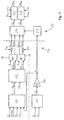
- FIG. 1 shows a single-phase converter.
- a three-phase DC / AC converter can be provided.
- the Figure 1 at the same time one leg of a three-phase modular multilevel converter.
- the in Figure 1 The converter shown has two converter branches 1, 2, which are each formed by a series connection of bridge modules 3 (here five bridge modules each). For each converter branch 1, 2, an inductance 6 is arranged in series with the series connection of the bridge modules 3.
- a bridge module 3 is shown in an enlarged view by way of example at the top right. Representing the other bridge modules 3, the internal structure with a half-bridge made of two power semiconductors 4 in the form of semiconductor switches, for example IGBTs, and a capacitor 5 is shown.
- the input voltage v dc is fed to the converter on the input side in the form of two half input voltages 7, 8, that is to say 1 ⁇ 2 v dc in each case.
- an output alternating voltage v ac is provided at the output 9 of the converter and an output current i ac is provided at the output 9 when the load is connected.
- Branch currents i b, 1 and i b, 2 flow in the converter branches 1, 2.
- the Figure 2 shows the converter according to Figure 1 in the form of an electrical equivalent circuit diagram, the input voltages 7, 8 being shown in the form of voltage sources with internal impedances, as well as the voltages v b, 1 and v b, 2 generated in the converter branches 1, 2.
- the circulating current i cir is the mean value of the two branch currents. This is made up of a constant direct current component i cir and an alternating current component ⁇ cir which is used to balance the energy in the converter branches 1, 2.
- the alternating output current i ac of the converter should be provided with a desired amplitude curve over time, a sinusoidal amplitude curve of an alternating current usually being desired.
- the invention is not limited to sinusoidal curves of the output alternating current; rather, other curves can also be implemented. In the following, however, the sinusoidal curve is assumed as an example.
- FIG Figure 3 Such a sinusoidal or at least approximately sinusoidal profile of the output alternating current i ac is shown in FIG Figure 3 recognizable. Incidentally, they show Figures 3 to 5 the same voltages and currents of the converter, only with different time resolutions.
- the Figure 4 is a first enlarged time scale compared to FIG Figure 3 is used, i.e. the signals are more finely resolved in terms of time.
- the output voltage v ac is shown with an even greater temporal resolution. Accordingly, the Figure 4 only a small time segment and, accordingly, only a few periods of the almost square-wave amplitude curves of the output voltage v ac .
- the time course with a rising edge of the output voltage v ac can be seen more clearly.
- the Figure 3 shows a complete period of the output alternating voltage v ac and the output alternating current i ac , which, as can be seen, is essentially sinusoidal, but with a certain ripple.
- the bridge modules 3 of the converter branches 1, 2 or their power semiconductors 4 are modulated at a higher frequency than the output frequency of the output AC voltage, which is shown in FIG Figure 3 can be recognized by the higher-frequency, essentially square-wave signal of the voltage v ac , which virtually envelops the sinusoidal curve of the output alternating current.
- This higher-frequency control takes place with a modulation frequency that is significantly higher than the output frequency, so that the voltage pulses generated in this way influence the output alternating current in the cycle of the modulation frequency alternately to larger and smaller values, so that on average the desired shows the amplitude curve of the output alternating current over time.
- This can take place by influencing a modulation parameter of the alternating modulation voltage v ac in some way, for example by the mark-to-space ratio, that is to say in the sense of a pulse duration modulation (PWM modulation). If the output alternating current is to be changed to larger values, the pulse duration of the modulation alternating voltage is increased, in the opposite case it is reduced.
- an alternating modulation voltage is generated with an amplitude of the essentially square-wave signal which corresponds to the maximum value that can be achieved with the input voltage v dc.
- All bridge modules connected in series are therefore always switched on and switched off again. This results in a maximum amplitude swing in the modulation AC voltage.
- a maximum reduction in the required capacitances, that is to say the capacitors 5, in the bridge modules 3 can be achieved.
- the circulating current can be guided and regulated in a certain way. In the context of the invention, however, it is not necessary to utilize the maximum modulation swing in the case of the modulation alternating voltage.
- a smaller modulation swing can also be generated, with which the temporal amplitude profile of the output alternating current can nevertheless be influenced in the desired manner, so that the desired temporal amplitude profile of the output alternating current is produced.
- the Figure 6 shows for the in the Figure 3 the time range shown the course of the circulating current i cir.
- the circulating current i cir takes on relatively large values at times, which makes it possible to keep the branch currents i b, 1 and i b, 2 low and thus to minimize the energy variation.
- branch currents it is advantageous to regulate the branch currents in such a way that they return the amounts of energy absorbed during the voltage edges while the branch voltages are high. A small, negative branch current is required for this.
- branch currents are thus routed in such a way that their magnitude essentially corresponds to that of the output current i ac when the branch voltages are low, and only a small branch current is available for regulating the branch energies when the branch voltages are high.
- the Figure 7 shows the structure of a control device for controlling the converter according to FIG Figure 1 .
- Switching signals are generated as output signals with which the gate connections of the power semiconductors 4 are controlled.
- the control device has a regulator part 24 and a modulator part 25.
- the regulator part 24 has an energy regulator 10 for each converter branch 1, 2, furthermore an output current regulator 11, a regulator for the circulating current 12, an amplifier 14, summing elements 18, 19 and blocks 16, 17, which are described in more detail below.
- the modulator part 25 has a switching unit 20, a PWM generator 21 and branch modulators 22, 23.
- the input and output currents are regulated independently of one another via the input current regulator 12 and the output current regulator 11.
- the length of a control cycle of the output current depends on the modulation frequency or the corresponding period of the PWM signal generated from it. In this sense, the PWM generator 21 is used to control and synchronize the branch modulators 22, 23.
- the measured output current i ac is regulated with reference to a reference value i * ac by means of the output current regulator 11, which can be designed as a PI regulator.
- the output value of the output current regulator 11 supplies an output voltage reference value v * ac. This is divided by the measured input voltage V dc (block 14), which leads to a modulation reference value m.
- the total branch energy of the converter branches 1, 2, characterized by the variables e b1 and e b2 is determined from the vector of the measured voltages of the capacitors 5 of the bridge modules 3. This is the sum of the energies that are stored in the capacitors of each converter branch. These branch energies are regulated by means of the energy regulator 10, which can also be designed as a PI regulator.
- the energy regulator 10 regulates the respective branch energy in relation to a branch energy reference value e * b , which can be set as a constant value and can be selected for a respective converter.
- the energy regulator 10 defines a reference power value for the respective converter branch as p * b, 1 or p * b, 2 .
- the branch power is set by the input current value. If a PWM pulse of the modulation AC voltage is present in the converter branch 1 (state T1), a circulating current reference value i * cir, T1 is obtained from the current reference value i * b1 of the converter branch 1 and the measured output current i ac .
- the circulating current reference value i * cir, T2 is obtained from the current reference value i * b2 of the converter branch 2 and the measured output current i ac when a PWM pulse of the modulation AC voltage is present in the converter branch 2 (state T2).
- Each input current reference value is fed to an independent part of the input current regulator 12, which can be implemented as a P regulator, for example.
- the output variables of the input current regulator 12 are multiplied separately in the blocks 16, 17 with the inverted state space matrix B, taking into account a further input variable.
- a switch is made between two groups of branch voltage reference values.
- the voltages v * b1, T1 and v * b2, T1 are used during a positive voltage pulse in the converter branch 1 (state T1), so in this case the measured input voltage value V dc is added to the value v * b1, T1 .
- the voltages v * b1, T2 and v * b2, T2 are used during the positive voltage pulse in the converter branch 2 (state T2), so the measured input voltage value is added to v * b2, T2 in this case.
- the modulator part 25 selects the respective combination of the branch voltage reference values v * b1 and v * b2 via the switch 20 in accordance with the currently valid state T1 or T2.
- the selection of the state T1 or T2 takes place in the modulator part 21 according to the modulation reference value m by means of a triangular carrier pulse duration modulation.
- the selected values are then modulated in the separate branch modulators 22, 23 to form the control signals s b1 and s b2.
- the sampling frequency of the output current regulator 11, the amplifier 14 and / or the PWM generator 21 can be selected to be significantly lower than that of the other previously explained blocks of the control device, in particular the regulating and / or modulator blocks, namely, for example, corresponding to the single or double modulation frequency , in the Fig. 3 can be recognized by the modulation alternating voltage.
- the sampling frequency of some or all of the other previously explained blocks of the control device, in particular the regulation and / or modulator blocks can be significantly higher than the modulation frequency in order to achieve a high quality of regulation of the circulating current.
- the number of switching operations can be distributed over the bridge modules 3 connected in series in a converter branch, so that the effects on the switching losses remain small.
Landscapes
- Engineering & Computer Science (AREA)
- Power Engineering (AREA)
- Inverter Devices (AREA)
Claims (11)
- Procédé pour faire fonctionner un convertisseur modulaire multi-niveaux qui comporte plusieurs branches de convertisseur (1, 2) dans chacune desquelles sont disposés des circuits série de modules en pont (3), les modules en pont (3) comportant chacun un circuit en pont sous la forme d'un demi-pont ou d'un pont complet de semi-conducteurs de puissance (4) et au moins un condensateur (5) qui peut être commuté par l'intermédiaire du circuit en pont, le procédé permettant de fournir une tension alternative de sortie (vac) avec une fréquence de sortie sur un côté sortie (9) du convertisseur,
caractérisé en ce que
l'évolution temporelle souhaitée de l'amplitude de la tension alternative de sortie (vac) du convertisseur est synthétisée par une tension alternative de modulation qui est générée par les modules en pont (3) d'une ou de plusieurs branches de convertisseur (1, 2), à une fréquence de modulation supérieure à la fréquence de sortie, au moyen d'une régulation à deux points dans laquelle toujours tous les modules en pont (3) d'une branche de convertisseur respective (1, 2) montés en série sont mis en circuit et recoupés,
la tension alternative de modulation passant alternativement en dessus et en dessous de la tension alternative de sortie (vac) selon le rythme de la fréquence de modulation, et
les instants de commutation des semi-conducteurs de puissance (4) des modules en pont (3) de cette branche de convertisseur (1, 2) sont régulés par un régulateur d'énergie respectif (10) associé à une branche de convertisseur (1, 2), avec pour objectif de minimiser la variation d'énergie de la branche de convertisseur (1, 2) en générant et en régulant un courant électrique circulaire (icir) dans le convertisseur. - Procédé selon la revendication précédente,
caractérisé en ce qu'un équilibrage du contenu énergétique dans une branche de convertisseur (1, 2) est effectué au sein d'une période de la tension alternative de modulation en générant le courant électrique circulaire (icir). - Procédé selon l'une des revendications précédentes,
caractérisé en ce que l'évolution temporelle souhaitée de l'amplitude de la tension alternative de sortie (vac) du convertisseur est générée par modulation de la durée d'impulsion de la tension alternative de modulation. - Procédé selon l'une des revendications précédentes,
caractérisé en ce que la tension alternative de modulation est générée en forme rectangulaire ou en forme de trapèze ou d'escalier à flancs raides. - Procédé selon l'une des revendications précédentes,
caractérisé en ce que le courant de sortie (iac) du convertisseur est commandé et/ou régulé indépendamment du courant électrique circulaire (icir). - Convertisseur modulaire multi-niveaux comportant plusieurs branches de convertisseur (1, 2) dans chacune desquelles sont disposés des circuits série de modules en pont (3), les modules en pont (3) comportant chacun un circuit en pont sous la forme d'un demi-pont ou d'un pont complet de semi-conducteurs de puissance (4) et au moins un condensateur (5) qui peut être commuté par l'intermédiaire du circuit en pont, et comportant au moins un dispositif de commande (24, 25) qui est conçu pour mettre en œuvre un procédé selon l'une des revendications précédentes.
- Convertisseur selon la revendication précédente,
caractérisé en ce que le dispositif de commande (24, 25) comprend un régulateur de courant de sortie (11) qui est conçu pour réguler le courant de sortie (iac) du convertisseur. - Convertisseur selon l'une des revendications 6 à 7,
caractérisé en ce que le dispositif de commande (24, 25) comprend un régulateur de courant circulaire (12) qui est conçu pour générer et réguler le courant électrique circulaire (icir) dans le convertisseur. - Convertisseur selon la revendication précédente,
caractérisé en ce que le régulateur de courant circulaire (12) est disposé en aval du régulateur de contenu énergétique (10). - Convertisseur selon l'une des revendications 6 à 9,
caractérisé en ce que le dispositif de commande (24, 25) présente au moins deux fréquences d'échantillonnage différentes auxquelles sont exploitées différentes parties du dispositif de commande (24, 25). - Programme d'ordinateur comprenant des moyens de code de programme, qui, lorsque le programme d'ordinateur est exécuté sur un ordinateur, est conçu pour faire fonctionner un convertisseur modulaire multi-niveaux qui comporte plusieurs branches de convertisseur (1, 2) dans chacune desquelles sont disposés des circuits série de modules en pont (3), les modules en pont (3) comportant chacun un circuit en pont sous la forme d'un demi-pont ou d'un pont complet de semi-conducteurs de puissance (4) et au moins un condensateur (5) qui peut être commuté par l'intermédiaire du circuit en pont, le procédé permettant de fournir une tension alternative de sortie (vac) avec une fréquence de sortie sur un côté sortie (9) du convertisseur,
dans lequel l'évolution temporelle souhaitée de l'amplitude de la tension alternative de sortie (vac) du convertisseur est synthétisée par une tension alternative de modulation qui est générée par les modules en pont (3) d'une ou de plusieurs branches de convertisseur (1, 2), à une fréquence de modulation supérieure à la fréquence de sortie, au moyen d'une régulation à deux points dans laquelle toujours tous les modules en pont (3) d'une branche de convertisseur respective (1, 2) montés en série sont mis en circuit et recoupés,
la tension alternative de modulation passant alternativement en dessus et en dessous de la tension alternative de sortie (vac) selon le rythme de la fréquence de modulation, et
les instants de commutation des semi-conducteurs de puissance (4) des modules en pont (3) de cette branche de convertisseur (1, 2) sont régulés au moyen d'un régulateur d'énergie respectif (10) associé à une branche de convertisseur (1, 2), avec pour objectif de minimiser la variation d'énergie de la branche de convertisseur (1, 2) en générant et en régulant un courant électrique circulaire (icir) dans le convertisseur.
Applications Claiming Priority (2)
| Application Number | Priority Date | Filing Date | Title |
|---|---|---|---|
| DE102015116271.7A DE102015116271A1 (de) | 2015-09-25 | 2015-09-25 | Verfahren zum Betrieb eines modularen Multilevel-Stromrichters, modularer Multilevel-Stromrichter sowie Computerprogramm |
| PCT/EP2016/072673 WO2017050960A1 (fr) | 2015-09-25 | 2016-09-23 | Procédé de fonctionnement d'un convertisseur de courant modulaire à multiples niveaux, convertisseur de courant modulaire à multiples niveaux ainsi que programme d'ordinateur |
Publications (2)
| Publication Number | Publication Date |
|---|---|
| EP3353885A1 EP3353885A1 (fr) | 2018-08-01 |
| EP3353885B1 true EP3353885B1 (fr) | 2021-04-28 |
Family
ID=56990443
Family Applications (1)
| Application Number | Title | Priority Date | Filing Date |
|---|---|---|---|
| EP16770497.2A Active EP3353885B1 (fr) | 2015-09-25 | 2016-09-23 | Procédé de fonctionnement d'un convertisseur de courant modulaire à multiples niveaux, convertisseur de courant modulaire à multiples niveaux ainsi que programme d'ordinateur |
Country Status (3)
| Country | Link |
|---|---|
| EP (1) | EP3353885B1 (fr) |
| DE (1) | DE102015116271A1 (fr) |
| WO (1) | WO2017050960A1 (fr) |
Families Citing this family (2)
| Publication number | Priority date | Publication date | Assignee | Title |
|---|---|---|---|---|
| DE102020108034B3 (de) * | 2019-12-05 | 2021-04-08 | Gottfried Wilhelm Leibniz Universität Hannover | Modularer Multilevel-Umrichter, Verfahren zum Betrieb von modularen Multilevel-Umrichtern und Computerprogramm |
| CN114793052A (zh) * | 2022-06-22 | 2022-07-26 | 国网山东省电力公司东营供电公司 | 模块化多电平变换器工作在准两电平模式下的换流方法 |
Family Cites Families (2)
| Publication number | Priority date | Publication date | Assignee | Title |
|---|---|---|---|---|
| DE102008014898B4 (de) * | 2008-03-19 | 2018-09-27 | Siemens Aktiengesellschaft | Verfahren zur Steuerung eines mehrphasigen Stromrichters mit verteilten Energiespeichern bei niedrigen Ausgangsfrequenzen |
| KR20150035501A (ko) | 2012-03-09 | 2015-04-06 | 커티스-라이트 일렉트로-메카니칼 코포레이션 | M2lc 시스템 및 이의 제어 방법 |
-
2015
- 2015-09-25 DE DE102015116271.7A patent/DE102015116271A1/de not_active Ceased
-
2016
- 2016-09-23 EP EP16770497.2A patent/EP3353885B1/fr active Active
- 2016-09-23 WO PCT/EP2016/072673 patent/WO2017050960A1/fr unknown
Non-Patent Citations (1)
| Title |
|---|
| None * |
Also Published As
| Publication number | Publication date |
|---|---|
| WO2017050960A1 (fr) | 2017-03-30 |
| DE102015116271A1 (de) | 2017-03-30 |
| EP3353885A1 (fr) | 2018-08-01 |
Similar Documents
| Publication | Publication Date | Title |
|---|---|---|
| EP1253706B1 (fr) | Circuit d'électronique de puissane et procédé pour transférer la puissance active | |
| DE102008014898A1 (de) | Verfahren zur Steuerung eines mehrphasigen Stromrichters mit verteilten Energiespeichern bei niedrigen Ausgangsfrequenzen | |
| DE102011083753A1 (de) | Vorrichtungen und Verfahren zur adaptiven Harmonischenreduzierung | |
| EP3136581B1 (fr) | Convertisseur de frequence multipoints modulaire et son procede de fonctionnement | |
| DE102020108035B3 (de) | Modularer Multilevel-Umrichter, Verfahren zum Betrieb von modularen Multilevel-Umrichtern und Computerprogramm | |
| EP2596980A2 (fr) | Convertisseur de courant à plusieurs points avec hacheur de freinage | |
| WO2013143793A2 (fr) | Circuit redresseur à injection de courant | |
| DE102005041825A1 (de) | Regelvorrichtung für eine dreiphasige Drehstrommaschine | |
| DE2446635A1 (de) | Wechselrichteranordnung mit zwei dreiphasigen steuerbaren wechselrichtern | |
| EP2863528A1 (fr) | Utilisation d'un onduleur comme un convertisseur CC/CC | |
| DE102007021368A1 (de) | Steuerverfahren | |
| EP4106176A1 (fr) | Procédé d'opération d'un onduleur multi-niveaux avec condensateurs volants | |
| EP3353885B1 (fr) | Procédé de fonctionnement d'un convertisseur de courant modulaire à multiples niveaux, convertisseur de courant modulaire à multiples niveaux ainsi que programme d'ordinateur | |
| EP3602762B1 (fr) | Onduleur | |
| EP4046268B1 (fr) | Détermination des paramètres de filtrage dans un onduleur | |
| EP2928060A1 (fr) | Circuit de convertisseur modulaire doté de sous-modules présentant différentes capacités de commutation | |
| EP3095178B1 (fr) | Circuit de convertisseur modulaire doté de sous-modules fonctionnant en mode linéaire | |
| DE19650994C1 (de) | Verfahren zur Pulsweitenmodulation einer Sollspannung für 3-Level-Vierquadrantensteller mit Berücksichtigung der Mindestschaltzeiten der Leistungshalbleiterschalter | |
| WO2013071947A1 (fr) | Convertisseur modulaire | |
| DE112015000929T5 (de) | Einrichtung und Verfahren zum Reduzieren von Oberschwingungen | |
| EP2928056B1 (fr) | Procédé et dispositif de fonctionnement d'un convertisseur de courant modulaire avec une grande vitesse de commutation ajustable | |
| EP3639352B1 (fr) | Ensemble convertisseur de puissance présentant une capacité de coupure d'un courant de fuite et procédé pour la coupure d'un courant de fuite pour ledit ensemble convertisseur de puissance | |
| EP2409394B1 (fr) | Procédé de fonctionnement d'un circuit convertisseur et dispositif pour la mise en uvre du procédé | |
| EP3556003B1 (fr) | Convertisseur multi-niveaux et procédé de fonctionnement | |
| EP2928055B1 (fr) | Convertisseur de courant modulaire et procédé de production d'une tension de sortie sinusoïdale à harmoniques réduites |
Legal Events
| Date | Code | Title | Description |
|---|---|---|---|
| STAA | Information on the status of an ep patent application or granted ep patent |
Free format text: STATUS: THE INTERNATIONAL PUBLICATION HAS BEEN MADE |
|
| PUAI | Public reference made under article 153(3) epc to a published international application that has entered the european phase |
Free format text: ORIGINAL CODE: 0009012 |
|
| STAA | Information on the status of an ep patent application or granted ep patent |
Free format text: STATUS: REQUEST FOR EXAMINATION WAS MADE |
|
| 17P | Request for examination filed |
Effective date: 20180306 |
|
| AK | Designated contracting states |
Kind code of ref document: A1 Designated state(s): AL AT BE BG CH CY CZ DE DK EE ES FI FR GB GR HR HU IE IS IT LI LT LU LV MC MK MT NL NO PL PT RO RS SE SI SK SM TR |
|
| AX | Request for extension of the european patent |
Extension state: BA ME |
|
| DAV | Request for validation of the european patent (deleted) | ||
| DAX | Request for extension of the european patent (deleted) | ||
| STAA | Information on the status of an ep patent application or granted ep patent |
Free format text: STATUS: EXAMINATION IS IN PROGRESS |
|
| 17Q | First examination report despatched |
Effective date: 20190821 |
|
| GRAP | Despatch of communication of intention to grant a patent |
Free format text: ORIGINAL CODE: EPIDOSNIGR1 |
|
| STAA | Information on the status of an ep patent application or granted ep patent |
Free format text: STATUS: GRANT OF PATENT IS INTENDED |
|
| INTG | Intention to grant announced |
Effective date: 20201202 |
|
| GRAS | Grant fee paid |
Free format text: ORIGINAL CODE: EPIDOSNIGR3 |
|
| GRAA | (expected) grant |
Free format text: ORIGINAL CODE: 0009210 |
|
| STAA | Information on the status of an ep patent application or granted ep patent |
Free format text: STATUS: THE PATENT HAS BEEN GRANTED |
|
| AK | Designated contracting states |
Kind code of ref document: B1 Designated state(s): AL AT BE BG CH CY CZ DE DK EE ES FI FR GB GR HR HU IE IS IT LI LT LU LV MC MK MT NL NO PL PT RO RS SE SI SK SM TR |
|
| REG | Reference to a national code |
Ref country code: GB Ref legal event code: FG4D Free format text: NOT ENGLISH |
|
| REG | Reference to a national code |
Ref country code: CH Ref legal event code: EP |
|
| REG | Reference to a national code |
Ref country code: AT Ref legal event code: REF Ref document number: 1388272 Country of ref document: AT Kind code of ref document: T Effective date: 20210515 |
|
| REG | Reference to a national code |
Ref country code: DE Ref legal event code: R096 Ref document number: 502016012927 Country of ref document: DE |
|
| REG | Reference to a national code |
Ref country code: IE Ref legal event code: FG4D Free format text: LANGUAGE OF EP DOCUMENT: GERMAN |
|
| REG | Reference to a national code |
Ref country code: LT Ref legal event code: MG9D |
|
| PG25 | Lapsed in a contracting state [announced via postgrant information from national office to epo] |
Ref country code: HR Free format text: LAPSE BECAUSE OF FAILURE TO SUBMIT A TRANSLATION OF THE DESCRIPTION OR TO PAY THE FEE WITHIN THE PRESCRIBED TIME-LIMIT Effective date: 20210428 Ref country code: BG Free format text: LAPSE BECAUSE OF FAILURE TO SUBMIT A TRANSLATION OF THE DESCRIPTION OR TO PAY THE FEE WITHIN THE PRESCRIBED TIME-LIMIT Effective date: 20210728 Ref country code: FI Free format text: LAPSE BECAUSE OF FAILURE TO SUBMIT A TRANSLATION OF THE DESCRIPTION OR TO PAY THE FEE WITHIN THE PRESCRIBED TIME-LIMIT Effective date: 20210428 Ref country code: LT Free format text: LAPSE BECAUSE OF FAILURE TO SUBMIT A TRANSLATION OF THE DESCRIPTION OR TO PAY THE FEE WITHIN THE PRESCRIBED TIME-LIMIT Effective date: 20210428 Ref country code: NL Free format text: LAPSE BECAUSE OF FAILURE TO SUBMIT A TRANSLATION OF THE DESCRIPTION OR TO PAY THE FEE WITHIN THE PRESCRIBED TIME-LIMIT Effective date: 20210428 |
|
| PG25 | Lapsed in a contracting state [announced via postgrant information from national office to epo] |
Ref country code: NO Free format text: LAPSE BECAUSE OF FAILURE TO SUBMIT A TRANSLATION OF THE DESCRIPTION OR TO PAY THE FEE WITHIN THE PRESCRIBED TIME-LIMIT Effective date: 20210728 Ref country code: PL Free format text: LAPSE BECAUSE OF FAILURE TO SUBMIT A TRANSLATION OF THE DESCRIPTION OR TO PAY THE FEE WITHIN THE PRESCRIBED TIME-LIMIT Effective date: 20210428 Ref country code: PT Free format text: LAPSE BECAUSE OF FAILURE TO SUBMIT A TRANSLATION OF THE DESCRIPTION OR TO PAY THE FEE WITHIN THE PRESCRIBED TIME-LIMIT Effective date: 20210830 Ref country code: RS Free format text: LAPSE BECAUSE OF FAILURE TO SUBMIT A TRANSLATION OF THE DESCRIPTION OR TO PAY THE FEE WITHIN THE PRESCRIBED TIME-LIMIT Effective date: 20210428 Ref country code: SE Free format text: LAPSE BECAUSE OF FAILURE TO SUBMIT A TRANSLATION OF THE DESCRIPTION OR TO PAY THE FEE WITHIN THE PRESCRIBED TIME-LIMIT Effective date: 20210428 Ref country code: LV Free format text: LAPSE BECAUSE OF FAILURE TO SUBMIT A TRANSLATION OF THE DESCRIPTION OR TO PAY THE FEE WITHIN THE PRESCRIBED TIME-LIMIT Effective date: 20210428 Ref country code: IS Free format text: LAPSE BECAUSE OF FAILURE TO SUBMIT A TRANSLATION OF THE DESCRIPTION OR TO PAY THE FEE WITHIN THE PRESCRIBED TIME-LIMIT Effective date: 20210828 Ref country code: GR Free format text: LAPSE BECAUSE OF FAILURE TO SUBMIT A TRANSLATION OF THE DESCRIPTION OR TO PAY THE FEE WITHIN THE PRESCRIBED TIME-LIMIT Effective date: 20210729 |
|
| REG | Reference to a national code |
Ref country code: NL Ref legal event code: MP Effective date: 20210428 |
|
| PG25 | Lapsed in a contracting state [announced via postgrant information from national office to epo] |
Ref country code: SK Free format text: LAPSE BECAUSE OF FAILURE TO SUBMIT A TRANSLATION OF THE DESCRIPTION OR TO PAY THE FEE WITHIN THE PRESCRIBED TIME-LIMIT Effective date: 20210428 Ref country code: SM Free format text: LAPSE BECAUSE OF FAILURE TO SUBMIT A TRANSLATION OF THE DESCRIPTION OR TO PAY THE FEE WITHIN THE PRESCRIBED TIME-LIMIT Effective date: 20210428 Ref country code: CZ Free format text: LAPSE BECAUSE OF FAILURE TO SUBMIT A TRANSLATION OF THE DESCRIPTION OR TO PAY THE FEE WITHIN THE PRESCRIBED TIME-LIMIT Effective date: 20210428 Ref country code: EE Free format text: LAPSE BECAUSE OF FAILURE TO SUBMIT A TRANSLATION OF THE DESCRIPTION OR TO PAY THE FEE WITHIN THE PRESCRIBED TIME-LIMIT Effective date: 20210428 Ref country code: DK Free format text: LAPSE BECAUSE OF FAILURE TO SUBMIT A TRANSLATION OF THE DESCRIPTION OR TO PAY THE FEE WITHIN THE PRESCRIBED TIME-LIMIT Effective date: 20210428 Ref country code: ES Free format text: LAPSE BECAUSE OF FAILURE TO SUBMIT A TRANSLATION OF THE DESCRIPTION OR TO PAY THE FEE WITHIN THE PRESCRIBED TIME-LIMIT Effective date: 20210428 Ref country code: RO Free format text: LAPSE BECAUSE OF FAILURE TO SUBMIT A TRANSLATION OF THE DESCRIPTION OR TO PAY THE FEE WITHIN THE PRESCRIBED TIME-LIMIT Effective date: 20210428 |
|
| REG | Reference to a national code |
Ref country code: DE Ref legal event code: R097 Ref document number: 502016012927 Country of ref document: DE |
|
| PLBE | No opposition filed within time limit |
Free format text: ORIGINAL CODE: 0009261 |
|
| STAA | Information on the status of an ep patent application or granted ep patent |
Free format text: STATUS: NO OPPOSITION FILED WITHIN TIME LIMIT |
|
| 26N | No opposition filed |
Effective date: 20220131 |
|
| REG | Reference to a national code |
Ref country code: BE Ref legal event code: MM Effective date: 20210930 |
|
| PG25 | Lapsed in a contracting state [announced via postgrant information from national office to epo] |
Ref country code: IS Free format text: LAPSE BECAUSE OF FAILURE TO SUBMIT A TRANSLATION OF THE DESCRIPTION OR TO PAY THE FEE WITHIN THE PRESCRIBED TIME-LIMIT Effective date: 20210828 Ref country code: MC Free format text: LAPSE BECAUSE OF FAILURE TO SUBMIT A TRANSLATION OF THE DESCRIPTION OR TO PAY THE FEE WITHIN THE PRESCRIBED TIME-LIMIT Effective date: 20210428 Ref country code: AL Free format text: LAPSE BECAUSE OF FAILURE TO SUBMIT A TRANSLATION OF THE DESCRIPTION OR TO PAY THE FEE WITHIN THE PRESCRIBED TIME-LIMIT Effective date: 20210428 |
|
| PG25 | Lapsed in a contracting state [announced via postgrant information from national office to epo] |
Ref country code: IT Free format text: LAPSE BECAUSE OF FAILURE TO SUBMIT A TRANSLATION OF THE DESCRIPTION OR TO PAY THE FEE WITHIN THE PRESCRIBED TIME-LIMIT Effective date: 20210428 Ref country code: IE Free format text: LAPSE BECAUSE OF NON-PAYMENT OF DUE FEES Effective date: 20210923 Ref country code: BE Free format text: LAPSE BECAUSE OF NON-PAYMENT OF DUE FEES Effective date: 20210930 Ref country code: LU Free format text: LAPSE BECAUSE OF NON-PAYMENT OF DUE FEES Effective date: 20210923 |
|
| REG | Reference to a national code |
Ref country code: AT Ref legal event code: MM01 Ref document number: 1388272 Country of ref document: AT Kind code of ref document: T Effective date: 20210923 |
|
| PG25 | Lapsed in a contracting state [announced via postgrant information from national office to epo] |
Ref country code: AT Free format text: LAPSE BECAUSE OF NON-PAYMENT OF DUE FEES Effective date: 20210923 |
|
| REG | Reference to a national code |
Ref country code: DE Ref legal event code: R082 Ref document number: 502016012927 Country of ref document: DE Representative=s name: MEISSNER BOLTE PATENTANWAELTE RECHTSANWAELTE P, DE |
|
| PG25 | Lapsed in a contracting state [announced via postgrant information from national office to epo] |
Ref country code: HU Free format text: LAPSE BECAUSE OF FAILURE TO SUBMIT A TRANSLATION OF THE DESCRIPTION OR TO PAY THE FEE WITHIN THE PRESCRIBED TIME-LIMIT; INVALID AB INITIO Effective date: 20160923 |
|
| PG25 | Lapsed in a contracting state [announced via postgrant information from national office to epo] |
Ref country code: CY Free format text: LAPSE BECAUSE OF FAILURE TO SUBMIT A TRANSLATION OF THE DESCRIPTION OR TO PAY THE FEE WITHIN THE PRESCRIBED TIME-LIMIT Effective date: 20210428 |
|
| PGFP | Annual fee paid to national office [announced via postgrant information from national office to epo] |
Ref country code: DE Payment date: 20230919 Year of fee payment: 8 |
|
| PGFP | Annual fee paid to national office [announced via postgrant information from national office to epo] |
Ref country code: GB Payment date: 20231025 Year of fee payment: 8 |
|
| PGFP | Annual fee paid to national office [announced via postgrant information from national office to epo] |
Ref country code: FR Payment date: 20231018 Year of fee payment: 8 Ref country code: CH Payment date: 20231101 Year of fee payment: 8 |
|
| PG25 | Lapsed in a contracting state [announced via postgrant information from national office to epo] |
Ref country code: MK Free format text: LAPSE BECAUSE OF FAILURE TO SUBMIT A TRANSLATION OF THE DESCRIPTION OR TO PAY THE FEE WITHIN THE PRESCRIBED TIME-LIMIT Effective date: 20210428 |