EP3352003B1 - Afficheur - Google Patents
Afficheur Download PDFInfo
- Publication number
- EP3352003B1 EP3352003B1 EP18151482.9A EP18151482A EP3352003B1 EP 3352003 B1 EP3352003 B1 EP 3352003B1 EP 18151482 A EP18151482 A EP 18151482A EP 3352003 B1 EP3352003 B1 EP 3352003B1
- Authority
- EP
- European Patent Office
- Prior art keywords
- light
- layer
- display device
- parts
- disposed
- Prior art date
- Legal status (The legal status is an assumption and is not a legal conclusion. Google has not performed a legal analysis and makes no representation as to the accuracy of the status listed.)
- Active
Links
Images





Classifications
-
- G—PHYSICS
- G02—OPTICS
- G02F—OPTICAL DEVICES OR ARRANGEMENTS FOR THE CONTROL OF LIGHT BY MODIFICATION OF THE OPTICAL PROPERTIES OF THE MEDIA OF THE ELEMENTS INVOLVED THEREIN; NON-LINEAR OPTICS; FREQUENCY-CHANGING OF LIGHT; OPTICAL LOGIC ELEMENTS; OPTICAL ANALOGUE/DIGITAL CONVERTERS
- G02F1/00—Devices or arrangements for the control of the intensity, colour, phase, polarisation or direction of light arriving from an independent light source, e.g. switching, gating or modulating; Non-linear optics
- G02F1/01—Devices or arrangements for the control of the intensity, colour, phase, polarisation or direction of light arriving from an independent light source, e.g. switching, gating or modulating; Non-linear optics for the control of the intensity, phase, polarisation or colour
- G02F1/13—Devices or arrangements for the control of the intensity, colour, phase, polarisation or direction of light arriving from an independent light source, e.g. switching, gating or modulating; Non-linear optics for the control of the intensity, phase, polarisation or colour based on liquid crystals, e.g. single liquid crystal display cells
- G02F1/133—Constructional arrangements; Operation of liquid crystal cells; Circuit arrangements
- G02F1/1333—Constructional arrangements; Manufacturing methods
- G02F1/1335—Structural association of cells with optical devices, e.g. polarisers or reflectors
- G02F1/133509—Filters, e.g. light shielding masks
- G02F1/133514—Colour filters
-
- C—CHEMISTRY; METALLURGY
- C08—ORGANIC MACROMOLECULAR COMPOUNDS; THEIR PREPARATION OR CHEMICAL WORKING-UP; COMPOSITIONS BASED THEREON
- C08G—MACROMOLECULAR COMPOUNDS OBTAINED OTHERWISE THAN BY REACTIONS ONLY INVOLVING UNSATURATED CARBON-TO-CARBON BONDS
- C08G59/00—Polycondensates containing more than one epoxy group per molecule; Macromolecules obtained by polymerising compounds containing more than one epoxy group per molecule using curing agents or catalysts which react with the epoxy groups
- C08G59/18—Macromolecules obtained by polymerising compounds containing more than one epoxy group per molecule using curing agents or catalysts which react with the epoxy groups ; e.g. general methods of curing
- C08G59/20—Macromolecules obtained by polymerising compounds containing more than one epoxy group per molecule using curing agents or catalysts which react with the epoxy groups ; e.g. general methods of curing characterised by the epoxy compounds used
- C08G59/22—Di-epoxy compounds
- C08G59/24—Di-epoxy compounds carbocyclic
- C08G59/245—Di-epoxy compounds carbocyclic aromatic
-
- G—PHYSICS
- G02—OPTICS
- G02F—OPTICAL DEVICES OR ARRANGEMENTS FOR THE CONTROL OF LIGHT BY MODIFICATION OF THE OPTICAL PROPERTIES OF THE MEDIA OF THE ELEMENTS INVOLVED THEREIN; NON-LINEAR OPTICS; FREQUENCY-CHANGING OF LIGHT; OPTICAL LOGIC ELEMENTS; OPTICAL ANALOGUE/DIGITAL CONVERTERS
- G02F1/00—Devices or arrangements for the control of the intensity, colour, phase, polarisation or direction of light arriving from an independent light source, e.g. switching, gating or modulating; Non-linear optics
- G02F1/01—Devices or arrangements for the control of the intensity, colour, phase, polarisation or direction of light arriving from an independent light source, e.g. switching, gating or modulating; Non-linear optics for the control of the intensity, phase, polarisation or colour
- G02F1/13—Devices or arrangements for the control of the intensity, colour, phase, polarisation or direction of light arriving from an independent light source, e.g. switching, gating or modulating; Non-linear optics for the control of the intensity, phase, polarisation or colour based on liquid crystals, e.g. single liquid crystal display cells
- G02F1/133—Constructional arrangements; Operation of liquid crystal cells; Circuit arrangements
- G02F1/1333—Constructional arrangements; Manufacturing methods
-
- C—CHEMISTRY; METALLURGY
- C08—ORGANIC MACROMOLECULAR COMPOUNDS; THEIR PREPARATION OR CHEMICAL WORKING-UP; COMPOSITIONS BASED THEREON
- C08G—MACROMOLECULAR COMPOUNDS OBTAINED OTHERWISE THAN BY REACTIONS ONLY INVOLVING UNSATURATED CARBON-TO-CARBON BONDS
- C08G59/00—Polycondensates containing more than one epoxy group per molecule; Macromolecules obtained by polymerising compounds containing more than one epoxy group per molecule using curing agents or catalysts which react with the epoxy groups
- C08G59/18—Macromolecules obtained by polymerising compounds containing more than one epoxy group per molecule using curing agents or catalysts which react with the epoxy groups ; e.g. general methods of curing
- C08G59/20—Macromolecules obtained by polymerising compounds containing more than one epoxy group per molecule using curing agents or catalysts which react with the epoxy groups ; e.g. general methods of curing characterised by the epoxy compounds used
- C08G59/32—Epoxy compounds containing three or more epoxy groups
- C08G59/38—Epoxy compounds containing three or more epoxy groups together with di-epoxy compounds
-
- C—CHEMISTRY; METALLURGY
- C09—DYES; PAINTS; POLISHES; NATURAL RESINS; ADHESIVES; COMPOSITIONS NOT OTHERWISE PROVIDED FOR; APPLICATIONS OF MATERIALS NOT OTHERWISE PROVIDED FOR
- C09D—COATING COMPOSITIONS, e.g. PAINTS, VARNISHES OR LACQUERS; FILLING PASTES; CHEMICAL PAINT OR INK REMOVERS; INKS; CORRECTING FLUIDS; WOODSTAINS; PASTES OR SOLIDS FOR COLOURING OR PRINTING; USE OF MATERIALS THEREFOR
- C09D163/00—Coating compositions based on epoxy resins; Coating compositions based on derivatives of epoxy resins
-
- G—PHYSICS
- G02—OPTICS
- G02F—OPTICAL DEVICES OR ARRANGEMENTS FOR THE CONTROL OF LIGHT BY MODIFICATION OF THE OPTICAL PROPERTIES OF THE MEDIA OF THE ELEMENTS INVOLVED THEREIN; NON-LINEAR OPTICS; FREQUENCY-CHANGING OF LIGHT; OPTICAL LOGIC ELEMENTS; OPTICAL ANALOGUE/DIGITAL CONVERTERS
- G02F1/00—Devices or arrangements for the control of the intensity, colour, phase, polarisation or direction of light arriving from an independent light source, e.g. switching, gating or modulating; Non-linear optics
- G02F1/01—Devices or arrangements for the control of the intensity, colour, phase, polarisation or direction of light arriving from an independent light source, e.g. switching, gating or modulating; Non-linear optics for the control of the intensity, phase, polarisation or colour
- G02F1/13—Devices or arrangements for the control of the intensity, colour, phase, polarisation or direction of light arriving from an independent light source, e.g. switching, gating or modulating; Non-linear optics for the control of the intensity, phase, polarisation or colour based on liquid crystals, e.g. single liquid crystal display cells
- G02F1/133—Constructional arrangements; Operation of liquid crystal cells; Circuit arrangements
- G02F1/1333—Constructional arrangements; Manufacturing methods
- G02F1/1335—Structural association of cells with optical devices, e.g. polarisers or reflectors
- G02F1/133509—Filters, e.g. light shielding masks
- G02F1/133514—Colour filters
- G02F1/133516—Methods for their manufacture, e.g. printing, electro-deposition or photolithography
-
- G—PHYSICS
- G02—OPTICS
- G02F—OPTICAL DEVICES OR ARRANGEMENTS FOR THE CONTROL OF LIGHT BY MODIFICATION OF THE OPTICAL PROPERTIES OF THE MEDIA OF THE ELEMENTS INVOLVED THEREIN; NON-LINEAR OPTICS; FREQUENCY-CHANGING OF LIGHT; OPTICAL LOGIC ELEMENTS; OPTICAL ANALOGUE/DIGITAL CONVERTERS
- G02F1/00—Devices or arrangements for the control of the intensity, colour, phase, polarisation or direction of light arriving from an independent light source, e.g. switching, gating or modulating; Non-linear optics
- G02F1/01—Devices or arrangements for the control of the intensity, colour, phase, polarisation or direction of light arriving from an independent light source, e.g. switching, gating or modulating; Non-linear optics for the control of the intensity, phase, polarisation or colour
- G02F1/13—Devices or arrangements for the control of the intensity, colour, phase, polarisation or direction of light arriving from an independent light source, e.g. switching, gating or modulating; Non-linear optics for the control of the intensity, phase, polarisation or colour based on liquid crystals, e.g. single liquid crystal display cells
- G02F1/133—Constructional arrangements; Operation of liquid crystal cells; Circuit arrangements
- G02F1/1333—Constructional arrangements; Manufacturing methods
- G02F1/1335—Structural association of cells with optical devices, e.g. polarisers or reflectors
- G02F1/133528—Polarisers
-
- G—PHYSICS
- G02—OPTICS
- G02F—OPTICAL DEVICES OR ARRANGEMENTS FOR THE CONTROL OF LIGHT BY MODIFICATION OF THE OPTICAL PROPERTIES OF THE MEDIA OF THE ELEMENTS INVOLVED THEREIN; NON-LINEAR OPTICS; FREQUENCY-CHANGING OF LIGHT; OPTICAL LOGIC ELEMENTS; OPTICAL ANALOGUE/DIGITAL CONVERTERS
- G02F1/00—Devices or arrangements for the control of the intensity, colour, phase, polarisation or direction of light arriving from an independent light source, e.g. switching, gating or modulating; Non-linear optics
- G02F1/01—Devices or arrangements for the control of the intensity, colour, phase, polarisation or direction of light arriving from an independent light source, e.g. switching, gating or modulating; Non-linear optics for the control of the intensity, phase, polarisation or colour
- G02F1/13—Devices or arrangements for the control of the intensity, colour, phase, polarisation or direction of light arriving from an independent light source, e.g. switching, gating or modulating; Non-linear optics for the control of the intensity, phase, polarisation or colour based on liquid crystals, e.g. single liquid crystal display cells
- G02F1/133—Constructional arrangements; Operation of liquid crystal cells; Circuit arrangements
- G02F1/1333—Constructional arrangements; Manufacturing methods
- G02F1/1335—Structural association of cells with optical devices, e.g. polarisers or reflectors
- G02F1/1336—Illuminating devices
- G02F1/133617—Illumination with ultraviolet light; Luminescent elements or materials associated to the cell
-
- C—CHEMISTRY; METALLURGY
- C09—DYES; PAINTS; POLISHES; NATURAL RESINS; ADHESIVES; COMPOSITIONS NOT OTHERWISE PROVIDED FOR; APPLICATIONS OF MATERIALS NOT OTHERWISE PROVIDED FOR
- C09K—MATERIALS FOR MISCELLANEOUS APPLICATIONS, NOT PROVIDED FOR ELSEWHERE
- C09K2323/00—Functional layers of liquid crystal optical display excluding electroactive liquid crystal layer characterised by chemical composition
- C09K2323/03—Viewing layer characterised by chemical composition
- C09K2323/031—Polarizer or dye
-
- C—CHEMISTRY; METALLURGY
- C09—DYES; PAINTS; POLISHES; NATURAL RESINS; ADHESIVES; COMPOSITIONS NOT OTHERWISE PROVIDED FOR; APPLICATIONS OF MATERIALS NOT OTHERWISE PROVIDED FOR
- C09K—MATERIALS FOR MISCELLANEOUS APPLICATIONS, NOT PROVIDED FOR ELSEWHERE
- C09K2323/00—Functional layers of liquid crystal optical display excluding electroactive liquid crystal layer characterised by chemical composition
- C09K2323/05—Bonding or intermediate layer characterised by chemical composition, e.g. sealant or spacer
- C09K2323/055—Epoxy
-
- G—PHYSICS
- G02—OPTICS
- G02F—OPTICAL DEVICES OR ARRANGEMENTS FOR THE CONTROL OF LIGHT BY MODIFICATION OF THE OPTICAL PROPERTIES OF THE MEDIA OF THE ELEMENTS INVOLVED THEREIN; NON-LINEAR OPTICS; FREQUENCY-CHANGING OF LIGHT; OPTICAL LOGIC ELEMENTS; OPTICAL ANALOGUE/DIGITAL CONVERTERS
- G02F1/00—Devices or arrangements for the control of the intensity, colour, phase, polarisation or direction of light arriving from an independent light source, e.g. switching, gating or modulating; Non-linear optics
- G02F1/01—Devices or arrangements for the control of the intensity, colour, phase, polarisation or direction of light arriving from an independent light source, e.g. switching, gating or modulating; Non-linear optics for the control of the intensity, phase, polarisation or colour
- G02F1/13—Devices or arrangements for the control of the intensity, colour, phase, polarisation or direction of light arriving from an independent light source, e.g. switching, gating or modulating; Non-linear optics for the control of the intensity, phase, polarisation or colour based on liquid crystals, e.g. single liquid crystal display cells
- G02F1/133—Constructional arrangements; Operation of liquid crystal cells; Circuit arrangements
- G02F1/1333—Constructional arrangements; Manufacturing methods
- G02F1/1335—Structural association of cells with optical devices, e.g. polarisers or reflectors
- G02F1/133509—Filters, e.g. light shielding masks
- G02F1/133514—Colour filters
- G02F1/133519—Overcoatings
-
- G—PHYSICS
- G02—OPTICS
- G02F—OPTICAL DEVICES OR ARRANGEMENTS FOR THE CONTROL OF LIGHT BY MODIFICATION OF THE OPTICAL PROPERTIES OF THE MEDIA OF THE ELEMENTS INVOLVED THEREIN; NON-LINEAR OPTICS; FREQUENCY-CHANGING OF LIGHT; OPTICAL LOGIC ELEMENTS; OPTICAL ANALOGUE/DIGITAL CONVERTERS
- G02F1/00—Devices or arrangements for the control of the intensity, colour, phase, polarisation or direction of light arriving from an independent light source, e.g. switching, gating or modulating; Non-linear optics
- G02F1/01—Devices or arrangements for the control of the intensity, colour, phase, polarisation or direction of light arriving from an independent light source, e.g. switching, gating or modulating; Non-linear optics for the control of the intensity, phase, polarisation or colour
- G02F1/13—Devices or arrangements for the control of the intensity, colour, phase, polarisation or direction of light arriving from an independent light source, e.g. switching, gating or modulating; Non-linear optics for the control of the intensity, phase, polarisation or colour based on liquid crystals, e.g. single liquid crystal display cells
- G02F1/133—Constructional arrangements; Operation of liquid crystal cells; Circuit arrangements
- G02F1/1333—Constructional arrangements; Manufacturing methods
- G02F1/1335—Structural association of cells with optical devices, e.g. polarisers or reflectors
- G02F1/133528—Polarisers
- G02F1/133548—Wire-grid polarisers
-
- G—PHYSICS
- G02—OPTICS
- G02F—OPTICAL DEVICES OR ARRANGEMENTS FOR THE CONTROL OF LIGHT BY MODIFICATION OF THE OPTICAL PROPERTIES OF THE MEDIA OF THE ELEMENTS INVOLVED THEREIN; NON-LINEAR OPTICS; FREQUENCY-CHANGING OF LIGHT; OPTICAL LOGIC ELEMENTS; OPTICAL ANALOGUE/DIGITAL CONVERTERS
- G02F2203/00—Function characteristic
- G02F2203/05—Function characteristic wavelength dependent
- G02F2203/055—Function characteristic wavelength dependent wavelength filtering
Definitions
- the present invention provides a display device with improved display quality and a method for manufacturing the same.
- the present inventive concept relates to a display device and a method for manufacturing the same, more particularly a liquid crystal display and a method for manufacturing the same.
- a display device includes a liquid crystal display (LCD), a plasma display panel (PDP), an electrophoretic display, and an organic light emitting diode (OLED) display, and the like.
- LCD liquid crystal display
- PDP plasma display panel
- OLED organic light emitting diode
- the liquid crystal display displays an image by using optical anisotropy and birefringence characteristics of liquid crystal molecules.
- an electric field is applied to the liquid crystal molecules, an arrangement of the liquid crystal molecules is changed, and a transmittance of light according to the changed arrangement direction of liquid crystal molecules may be changed.
- a liquid crystal display includes a color filter layer for representing a color, and the color filter layer may include a quantum dot to improve a light efficiency. Since the quantum dot has high color purity and color reproducibility, the liquid crystal display may provide a high quality color.
- CN 105182594A describes a liquid crystal display device comprising a planarization layer on a quantum dot layer.
- the planarization layer may be made from an epoxy resin.
- WO 96/34303 describes a material for forming a color-filter protecting film obtained from, inter alia, a cardo-based resin, an epoxy monomer, and a bisphenol A-type epoxy resin.
- the present invention provides a display device according to appended claim 1. Preferred embodiments are defined in the appended dependent claims.
- the word "comprise” or “has” is used to specify existence of a feature, a numbers, a process, an operation, a constituent element, a part, or a combination thereof, and it will be understood that existence or additional possibility of one or more other features or numbers, processes, operations, constituent elements, parts, or combinations thereof are not excluded in advance.
- an element such as a layer, film, region, or substrate is referred to as being “on” another element, it can be directly on the other element or intervening elements may also be present.
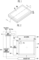
- FIG. 1 is a schematic perspective view of a display device according to an exemplary embodiment of the present inventive concept
- FIG. 2 is a schematic block diagram of a display device according to an exemplary embodiment of the present inventive concept.
- a display device may be provided various shapes, for example a rectangular-plate shape having two pairs of sides parallel with each other, but the display device is not limited thereto.
- the display device is provided as the rectangular-plate shape, one pair of sides selected from two pairs of sides may be longer than the other pair of sides.
- the display device may comprise a display panel DP comprising a plurality of pixel PXL and a backlight unit BLU providing light to the display panel DP.
- the display device may be a liquid crystal display in which the pixel PXL is implemented as a liquid crystal display element.
- the display panel DP comprises a display area DA and a non-display area NDA disposed at least one side of the display area DA.
- the display area DA may be an area displaying an image by disposing a pixel unit PP.
- the display area DA may have various shapes.
- the display area DA may have a polygon shape having sides made of straight lines.
- the display area DA may have a circular shape or an elliptical shape having a side made of a curved line.
- the display area DA may have a semicircular shape or a semi-elliptical shape having sides made of a straight line and a curved line.
- the pixel unit PP comprises the pixels PXL connected to gate lines GL1-GLn and data lines DL1-DLm.
- Each pixel PXL may be connected to a corresponding gate line GL1 of the gate lines GL1-GLn and a corresponding data line DL1 of the data lines DL1-DLm.
- Each pixel PXL may comprise a thin film transistor, a liquid crystal capacitor, a storage capacitor, and pixel electrode. Each pixel PXL will be described later.
- the non-display area NDA is an area in which no image is displayed.
- a driver may be disposed in the non-display area NDA.
- the driver may comprise a gate driver GDV, a data driver DDV, a timing controller TC, a backlight dimming controller BDC, and the like, and may be disposed on the same substrate as the display area DA or may be disposed on separate element (e.g., a printed circuit board).
- the timing controller TC receives a digital video data from an external system (not shown) through interfaces such as a Low Voltage Differential Signaling (LVDS) interface, a Transition Minimized Differential Signaling (TMDS) interface, and the like.
- the timing controller TC receives a vertical synchronization signal Vsync, a horizontal synchronization signal Hsync, a data enable signal DE, and a clock signal Clk from the external system.
- the timing controller TC may generate a gate control signal GCS and a data control signal DCS which respectively control the gate driver GDV and the data driver DDV by using the signals.
- the gate driver GDV may apply a scan signal to the gate lines GL1-GLn in response to the gate control signal GCS generated from the timing controller TC. For example, the gate driver GDV may sequentially supply the scan signal to the gate lines GL1-GLn. When the scan signal is sequentially supplied to the gate lines GL1-GLn, the pixels PXL may be selected in units of horizontal lines.
- the data driver DDV may supply a data signal of one line for each horizontal period to the data lines DL1-DLm in response to the data control signal DCS generated from the timing controller TC.
- the data signals applied to the data lines DL1-DLm may be supplied to the pixels PXL selected by the scan signals.
- the data driver DDV may supply the data signal to the data lines DL1-DLm so as to be synchronized with the scan signal.
- the backlight dimming controller BDC may determine a dimming duty of a light source (not shown) disposed in the backlight unit BLU.
- the backlight unit BLU is disposed under the display panel DP, and driven by the backlight dimming controller BDC to illuminate the display panel DP.
- the backlight unit BLU may comprise a light source providing light to the display panel DP, and optic members converting light supplied from the light source into surface light.
- the backlight unit BLU is shown as a plate shape in the drawing, this is for convenience of description and is not limited thereto.
- the backlight unit BLU may be formed as a direct type or an edge type.
- FIG. 3 is an equivalent circuit diagram illustrating an exemplary embodiment of a pixel shown in FIG. 2
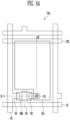
- FIG. 4A is a detailed plan view of a pixel shown in FIG. 3
- FIG. 4B is a cross-sectional view taken along line II-II' of FIG. 4A .
- a display device includes a plurality of signal lines and a plurality of pixels connected to the corresponding signal lines and arranged in a matrix form.
- FIGS. 4A and 4B disclose only one pixel of the pixels.
- the pixel is illustrated as a rectangular shape, but is not limited thereto, and may have various shapes.
- the signal lines include a gate line GL for transmitting a gate signal and a data line DL for transmitting a data signal.
- the gate line GL extends in a first direction (e.g., a row direction), and the data line DL extends in a second direction (e.g., a column direction) crossing the first direction.
- the pixel PXL includes a thin film transistor TFT connected to the gate line GL and the data line DL, a liquid crystal capacitor Clc, and a storage capacitor Cst.
- a gate electrode GE of the thin film transistor TFT is connected to the gate line GL, a source electrode SE of the thin film transistor TFT is connected to the data line DL, and a drain electrode DE of the thin film transistor TFT is connected to the liquid crystal capacitor Clc and the storage capacitor Cst connected to a storage line STL.
- the thin film transistor TFT When the gate signal is applied to the gate electrode GE, the thin film transistor TFT is turned on, and the data signal is stored in the liquid crystal capacitor Clc and the storage capacitor Cst connected together to the drain electrode DE.
- the storage capacitor Cst charges the data signal and maintains the data signal even after the thin film transistor TFT is turned off.
- a display device includes a first substrate SUB1, a second substrate SUB2 facing the first substrate SUB1, and a liquid crystal layer LC disposed between the first substrate SUB1 and the second substrate SUB2.
- the first substrate SUB1 including a plurality of pixels may include a first base substrate BS1, a thin film transistor TFT disposed on the first base substrate BS1, a first electrode EL1 connected to the thin film transistor TFT, and a first polarization layer POL1 disposed under the first base substrate BS1.
- each pixel PXL may include the thin film transistor TFT and the first electrode EL1 connected to the thin film transistor TFT.
- the first base substrate BS1 may be a rigid substrate or a flexible substrate.
- the rigid substrate may be one of a glass substrate, a quartz substrate, a glass ceramic substrate, and a crystalline substrate.
- the flexible substrate may be one of a film substrate comprising a polymer organic material and a plastic substrate. It is preferable that a material applied to the first base substrate BS1 has resistance (or heat resistance) to a high processing temperature in a manufacturing process.
- a gate line unit may be disposed on the first base substrate BS1.
- the gate line unit comprises a gate line GL, a gate electrode GE connected to the gate line GL, and the storage line STL.
- the gate line unit may be made of a metal.
- the gate line unit may be made of at least one of metals such as gold (Au), silver (Ag), aluminum (Al), molybdenum (Mo), chromium (Cr), titanium (Ti), nickel (Ni), neodymium (Nd), copper (Cu), or alloys of the metals.
- the gate line unit may be formed of a single layer, but embodiment is not limited thereto.
- the gate line unit may be formed of a multiple layer in which two or more of the metals and the alloys are stacked.
- a buffer layer (not shown) is disposed between the first base substrate BS1 and the gate line unit.
- the buffer layer prevents impurities from diffusing into the thin film transistor TFT.
- the buffer layer may have a single layer or at least two or more multiple layer.
- the buffer layer may be an inorganic insulating layer made of an inorganic material.
- the buffer layer may be formed of silicon nitride, silicon oxide, silicon oxynitride, or the like.
- each layer may be formed of the same material or may be formed of different material.
- the buffer layer may be omitted according to a material of the first base substrate BS1 and a process condition.
- a gate insulating layer GI is disposed on the gate line unit.
- the gate insulating layer GI may be an inorganic insulating layer made of an inorganic material.
- the inorganic material may comprise polysiloxane, silicon nitride, silicon oxide, silicon oxynitride, or the like.
- a semiconductor layer SML is disposed on the gate insulating layer GI.
- the semiconductor layer SML may be provided in a thin film shape on the gate insulating layer GI.
- the semiconductor layer SML is disposed on the gate electrode GE and may overlap at least a portion of the gate electrode GE.
- the semiconductor layer SML may be a semiconductor pattern made of polysilicon, amorphous silicon, oxide semiconductor, or the like.
- a data line unit is disposed on the semiconductor layer SML.
- the data line unit comprises a data line DL, a source electrode SE, and a drain electrode DE spaced apart from the source electrode SE.
- the source electrode SE may cover one side of the semiconductor layer SML, and the drain electrode DE may also cover the opposite side facing the one side of the semiconductor layer SML.
- the data line unit may be made of a conductive material, for example a metal.
- the data line unit may be formed of a single metal, or may be formed of two or more kinds of metals or alloys of two or more kinds of metals.
- the source electrode SE and the drain electrode DE may be made of nickel, chromium, molybdenum, aluminum, titanium, copper, tungsten, and an alloy thereof.
- each of the source electrode SE and the drain electrode DE may be formed of a single layer or a multiple layer.
- each of the source electrode SE and the drain electrode DE may be formed of a double layer made of titanium and copper.
- a passivation layer PSV is disposed on the data line unit.
- the passivation layer PSV may be formed of an inorganic insulating layer made of an inorganic material or an organic insulating layer made of an organic material.
- the inorganic material may comprise polysiloxane, silicon nitride, silicon oxide, silicon oxynitride, or the like.
- the organic material may comprise an organic insulating material such as a polyacryl-based compound, a polyimide-based compound, a fluorocarbon compound such as Teflon, a benzocyclobutene compound, and the like.
- the passivation layer PSV may comprise a contact hole exposing a portion of the drain electrode DE.
- the first electrode EL1 is disposed on the passivation layer PSV.
- the first electrode EL1 is connected to the drain electrode DE through the contact hole CH.
- the first electrode EL1 may be formed of a transparent conductive material.
- the first electrode E1 may be formed of a transparent conductive oxide.
- the transparent conductive oxide may comprise an indium tin oxide (ITO), an indium zinc oxide (IZO), an indium tin zinc oxide (ITZO), or the like.
- the first polarizer POL1 is disposed on a back surface of the first base substrate BS1 (for example, a surface on which the thin film transistor TFT is not disposed).
- the first polarizer POL1 polarizes light in a specific direction and provides the light to the liquid crystal layer LC while minimizing a loss of light provided from a backlight unit (not shown).
- the first electrode EL1 partially overlaps the storage line STL, and the first electrode EL1 and the storage line STL constitutes the storage capacitor Cst with the passivation layer PSV disposed therebetween.
- the second substrate SUB2 comprises a second base substrate BS2, a color conversion layer CFL disposed on the second base substrate BS2, an overcoat layer OC disposed on the color conversion layer CFL, a second polarization layer POL2 disposed on the overcoat layer OC, and a second electrode EL2 disposed on the second polarization layer POL2.
- the second base substrate BS2 may be formed of a transparent insulating material, for example, glass, silicon, quartz, plastic, or the like, and may have flexibility.
- the second base substrate BS2 may be made of the same material as the first base substrate BS1.
- the color conversion layer CFL transmits or converts light so that light provided from the backlight unit displays a specific color for each pixel PXL.
- the color conversion layer CFL may comprise a plurality of color filters CF displaying different colors depending on each pixel, and a black matrix BM disposed between color filters CF.
- the black matrix BM is formed between the color filters CF in the display area, and blocks light passing through the liquid crystal layer LC between adjacent pixels.
- An overcoat layer OC is disposed on the color conversion layer CFL.
- the overcoat layer OC may be made of an insulating material comprising epoxy polymer.
- the overcoat layer is disposed on the color conversion layer CFL to planarize an upper surface of the color conversion layer CFL.
- the overcoat layer is formed of an epoxy material which can planarize before curing regardless of topography of the upper surface of the color conversion layer CFL and a good reflow characteristic when curing.
- the epoxy polymer is obtainable by polymerising a cardo-based binder resin, an epoxy-based monomer comprising at least one of the compounds represented by the following chemical formulae: and a bisphenol A-based resin, wherein the cardo-based binder resin comprises compounds represented by Chemical Formula 1.
- Chemical Formula 1 wherein, n is a natural number in which the cardo-based binder resin has a molecular weight (e.g. a weight average molecular weight or a number average molecular weight) of 5,000 to 20,000.
- the epoxy polymer is provided in a total amount of 100 parts by weight of the epoxy polymer, and the amount of the cardo-based binder resin, the epoxy-based monomer, and the bisphenol A-based resin may be changed in a range of 20 to 40 parts by weight, 10 to 30 parts by weight, and 1 to 50 parts by weight, respectively.
- the cardo-based binder resin is a compound represented by Chemical Formula 1. wherein, n is a natural number in which the cardo-based binder resin has a molecular weight (e.g. a weight average molecular weight or a number average molecular weight) of 5,000 to 20,000.
- the epoxy polymer may contain 20 to 40 parts by weight of the cardo-based binder resin.
- the epoxy-based monomer may have a molecular weight of about 100 to about 400, and may have a glass transition temperature (Tg) of about 120 °C to about 200 °C. If the molecular weight of the epoxy-based monomer is small or excessively large, reflow characteristic deteriorates when the overcoat layer is formed. When a Tg of the epoxy-based monomer is lower than 120 °C, the epoxy-based monomer may have low heat resistance, and when the Tg is higher than 200 °C, a modification of the epoxy-based monomer may occur.
- the epoxy-based monomer comprises at least one of compounds represented by the following chemical formulae:
- the epoxy polymer contains 10 to 30 parts by weight of the epoxy-based monomer.
- the bisphenol-based resin is a bisphenol A-based resin.
- the bisphenol A-based resin is contained in the epoxy polymer in an amount of 15 to 25 parts by weight.
- the epoxy polymer may further comprise at least one of a bisphenol F-based resin, a novolac resin, and an aliphatic epoxy resin in addition to the cardo-based binder resin, the epoxy-based monomer, and the bisphenol A-based resin.
- at least one of the bisphenol F-based resin, the novolac resin, and the aliphatic epoxy resin may be contained in an amount of 20 to 30 parts by weight.
- the overcoat layer comprises a curing agent for curing a cardo-based epoxy binder, an epoxy-based monomer, a bisphenol-based resin, or the like.
- the curing agent may be contained in an amount of 60 to 120 parts by weight based on 100 parts by weight of the epoxy polymer.
- the curing agent may be a compound represented by Chemical Formula 3.
- the second polarization layer POL2 is disposed on the overcoat layer OC.
- the second polarization layer POL2 may polarize light passing through the first polarization layer POL1 and the liquid crystal layer LC in a specific direction to provide the light to the color conversion layer CFL.
- the second polarization layer POL2 may be a wire grid polarizer in which line lattice patterns (not shown) are spaced apart from each other by a predetermined distance.
- the second polarization layer POL2 may be an attaching type polarization layer or a coating type polarization layer, but is not limited thereto.
- the second electrode EL2 is disposed on the first polarization layer POL2.
- the second electrode EL2 is a common electrode forming an electric field together with the first electrode EL1.
- the second electrode EL2 is formed of a transparent conductive material.
- the second electrode EL2 may be formed of conductive metal oxide such as an indium tin oxide (ITO), an indium zinc oxide (IZO), an indium tin zinc oxide (ITZO), or the like.
- the second electrode EL2 generates an electric field together with the first electrode EL1 to drive the liquid crystal layer LC.
- the liquid crystal layer LC is disposed between the first substrate SUB1 and the second substrate SUB2, more particularly between the first electrode EL1 and the second electrode EL2.
- an alignment layer may be disposed between the first substrate SUB1 and the liquid crystal layer LC and/or between the second substrate SUB2 and the liquid crystal layer LC.
- the alignment layer may align liquid crystal molecules in the liquid crystal layer LC in a specific direction.
- a first alignment layer is disposed between the first substrate SUB1 and the liquid crystal layer LC
- a second alignment layer is disposed between the second substrate SUB2 and the liquid crystal layer LC.
- the liquid crystal layer LC comprises liquid crystal molecules having a negative dielectric anisotropy, and displays an image by changing a transmittance of light based on an electric field formed between the pixel electrode and the common electrode.
- the thin film transistor when the gate signal is applied to the gate line, the thin film transistor is turned on. Therefore, the data signal applied to the data line is applied to the first electrode through the thin film transistor.
- the thin film transistor When the thin film transistor is turned on and the data signal is applied to the first electrode, an electric field is formed between the first electrode and the second electrode.
- the liquid crystal molecules are driven by the electric field generated due to a difference between a voltage applied to the second electrode and a voltage applied to the first electrode. Accordingly, an amount of light passing through the liquid crystal layer is changed to display an image.
- FIG. 5 is a schematic cross-sectional view of three adjacent pixels in a display device according to an exemplary embodiment of the present inventive concept.
- a display device may comprise a plurality of pixels displaying different colors.
- a display device may comprise first to third pixels PXL1, PXL2, and PXL3 providing different color images.
- the first to third pixels PXL1, PXL2, and PXL3 may comprise first to third color filters CF1, CF2, and CF3 which respectively represents first to third colors which are different colors each other in the color conversion layer CFL.
- Colors represented by the first to third color filters CF1, CF2, and CF3 may be respectively blue, green, and red.
- the colors represented by the color filters are not limited thereto, and various colors such as white, yellow, cyan, magenta, and the like may be displayed.
- the color conversion layer CFL may comprise a light conversion material which absorbs light emitted from a backlight unit and then converts the light into light of other color.
- the light conversion material when the light emitted from the backlight unit is referred to as first light, the light conversion material can convert the first light into second light or third light having a wavelength different from that of the first light.
- the kind of the light conversion material is not particularly limited as long as it can absorb light of a wavelength band emitted from the backlight unit and emit light of a different wavelength band.
- the light conversion material may be phosphor or a quantum dot.
- the quantum dot can emit green light and red light having a narrow full width of half maximum (FWHM) as compared with phosphor generally used as a light conversion material, thereby increasing a color reproduction ratio. Therefore, the light conversion material may be the quantum dot.
- the quantum dot may be selected from a group II-VI compound, a group III-V compound, a group IV-VI compound, a group IV element, a group IV compound, and a combination thereof.
- the group II-VI compound may be selected from: a group of two-element compounds selected from CdSe, CdTe, ZnS, ZnSe, ZnTe, ZnO, HgS, HgSe, HgTe, MgSe, MgS, and a mixture thereof; a group of three-element compounds selected from CdSeS, CdSeTe, CdSTe, ZnSeS, ZnSeTe, ZnSTe, HgSeS, HgSeTe, HgSTe, CdZnS, CdZnSe, CdZnTe, CdHgS, CdHgSe, CdHgTe, HgZnS, HgZnSe, HgZnTe, MgZnSe, MgZnS, and a mixture thereof; and a group of four-element compounds selected from HgZnTeS, CdZnSeS, CdZ
- the group III-V compound may be selected from: a group of two-element compounds selected from GaN, GaP, GaAs, GaSb, AlN, AlP, AlAs, AlSb, InN, InP, InAs, InSb, and a mixture thereof; a group of three-element compounds selected from GaNP, GaNAs, GaNSb, GaPAs, GaPSb, AlNP, AlNAs, AlNSb, AlPAs, AlPSb, InNP, InNAs, InNSb, InPAs, InPSb, GaAlNP, and a mixture thereof; and a group of four-element compounds selected from GaAlNAs, GaAlNSb, GaAlPAs, GaAlPSb, GaInNP, GaInNAs, GaInNSb, GaInPAs, GaInPSb, InAlNP, InAlNAs, InAlNSb, InAlPAs, InAlPSb, and a mixture thereof.
- the group IV-VI compound may be selected from: a group of two-element compounds selected from SnS, SnSe, SnTe, PbS, PbSe, PbTe, and a mixture thereof; a group of three-element compounds selected from SnSeS, SnSeTe, SnSTe, PbSeS, PbSeTe, PbSTe, SnPbS, SnPbSe, SnPbTe, and a mixture thereof; and a group of four-element compounds selected from SnPbSSe, SnPbSeTe, SnPbSTe, and a mixture thereof.
- the group IV element may be selected from a group of Si, Ge, and a mixture thereof.
- the group IV compound may be a two-element compound selected from a group of SiC, SiGe, and a mixture thereof.
- the two-element compounds, the three-element compounds or the four-element compounds may be present in a particle at the same concentration, or may be present in the same particle at a partially different concentration.
- the quantum dot may have a core/shell structure in which one quantum dot surrounds other quantum dot.
- An interface between a core and a shell may have a concentration gradient in which a concentration of an element existing in the shell becomes lower toward the center.
- the quantum dot may have a full width of half maximum (FWHM) of a emission wavelength spectrum of about 45nm or less, preferably about 40nm or less, more preferably about 30nm or less, and color purity or color reproducibility may be improved in this range.
- FWHM full width of half maximum
- light emitted through the quantum dot is emitted in all directions, so that a viewing angle may be improved.
- a shape of the quantum dot is not limited to a shape commonly used in the art, and may be in a shape of spherical, pyramidal, multi-arm, or cubic nanoparticle, nanotube, nanowire, nanofiber, nanoplate particle, and the like.
- the first color filter CF1 when the first light emitted from the backlight unit is blue light, the first color filter CF1 may represent a blue color by transmitting the first light. In this case, since a wavelength band of the first light does not need to be converted in the first color filter CF1, a separate light conversion material may not be required in the first color filter CF1. However, the first color filter CF1 may further comprise a material for increasing color purity if necessary. According to an exemplary embodiment of the present inventive concept, the first color filter CF1 may further comprise a blue dye or blue pigment representing a blue color.
- the first color filter CF1 may further comprise an additional material for improving uniformity of the light emitted from the first color filter CF1, light emitted from a second color filter CF2 and third color filter CF3 which will be described later.
- the first color filter CF1 may further comprise scatterers for controlling light distribution of light transmitting the first color filter CF1.
- the scatterers may be made of various materials, for example titanium oxide (TiO2).
- TiO2 titanium oxide
- the second color filter CF2 may comprise a light conversion material which absorbs the first light to represent the second light, i.e., green light.
- the light conversion material may be a first quantum dot QD1 which absorbs blue light and then, emits green light.
- the third color filter CF3 may comprise a light conversion material which absorbs the first light to represent the third light, i.e., red light.
- the light conversion material may be a second quantum dot QD2 which absorbs blue light and then, emits red light.
- each of the first quantum dot QD1 and the second quantum dot QD2 may be selected from one or more of the quantum dots described above.
- a display device may display color images.
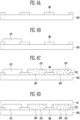
- FIGS. 6A to 6F are cross-sectional views sequentially illustrating a method for manufacturing a display device according to an exemplary embodiment of the present inventive concept.
- a second substrate SUB2 is prepared and a black matrix BM is formed on the second substrate SUB2.
- the black matrix BM may be formed of carbon, titanium oxide, iron oxide, or a mixture thereof.
- the type of the black matrix BM is not limited to materials for blocking light.
- the black matrix BM may be formed by forming the materials on the second base substrate BS2 and patterning the materials by a photolithography process, but embodiments are not limited thereto.
- a first color filter CF1 is formed on the second substrate SUB2.
- the first color filter CF1 is formed at a position corresponding to a first pixel.
- the first color filter CF1 may partially overlap the black matrix BM disposed on both sides thereof.
- the first color filter CF1 may be made of a material which transmits light.
- the first color filter CF1 may be formed by using an inkjet, a slit coating, photolithography, and the like, but is not limited thereto.
- a second color filter CF2 and a third color filter CF3 are formed on the second substrate SUB2.
- the second color filter CF2 and the third color filter CF3 may be formed separately or simultaneously, and each of the second color filter CF2 and the third color filter CF3 may comprise a different light conversion material (e.g., a quantum dot).
- the second color filter CF2 and the third color filter CF3 may be formed by using an inkjet, a slit coating, a photolithography, and the like, but is not limited thereto.
- the first color filter CF1, the second color filter CF2 and the third color filter CF3 may be formed simultaneously, for example, using an inkjet.
- an overcoat layer OC is formed on a color conversion layer CFL which made of the black matrix BM and the first to third color filters CF1, CF2, and CF3.
- the overcoat layer OC may be manufactured by forming a composition for forming an epoxy polymer on the second substrate SUB2 and curing the composition through a baking process.
- the baking process may proceed in a single process or in a multiple process.
- the curing process may be performed in a manner which applies heat to the composition.
- the composition may comprise a solvent and a solid comprising an epoxy-based material dispersed in the solvent.
- the solvent may be contained in an amount of about 73 wt% to 80 wt%
- the solid may be contained in an amount of about 20 wt% to 27 wt%, based on 100 wt% of a solution.
- the type of the solvent is not particularly limited, and various solvents in the art may be used.
- the solvent may comprise ketones such as acetone, methyl ethyl ketone and cyclohexanone, acetic acid esters such as ethyl acetate, butyl acetate, cellosolve acetate, propylene glycol monomethyl ether acetate and carbitol acetate, carbitols such as cellosolve and butyl carbitol, aromatic hydrocarbons such as solvent naphtha, toluene and xylene, amide solvents such as dimethylformamide, dimethylacetamide and N-methylpyrrolidone, and a combination of two or more thereof.
- ketones such as acetone, methyl ethyl ketone and cyclohexanone
- acetic acid esters such as ethyl acetate, butyl acetate, cellosolve acetate, propylene glycol mono
- the solid comprises a cardo-based binder resin, an epoxy-based monomer comprising at least one of the compounds represented by the following chemical formulae: a bisphenol A-based resin, wherein the cardo-based binder resin comprises compounds represented by Chemical Formula 1: wherein, n is a natural number in which the cardo-based binder resin has a molecular weight of 5,000 to 20,000, and a curing agent.
- the curing agent may be provided in an amount of 60 to 120 parts by weight based on 100 parts by weight of the epoxy polymer.
- the cardo-based binder resin, the epoxy-based monomer, and the bisphenol A-based resin may be respectively provided in an amount of 20 to 40 parts by weight, 10 to 30 parts by weight, and 15 to 25 parts by weight, based on 100 parts by weight of the epoxy polymer.
- the composition is provided with a fluid having a predetermined viscosity
- the composition may be coated on the color filters and fill gaps between adjacent color filters to have a flattened surface.
- the composition is then reflowed during a thermal curing process to further planarize the surface of the composition.
- the composition comprises the epoxy polymer, a shrinkage rate of the composition is low. Therefore, the overcoat layer OC is formed to have a planarized surface.
- the solvent is removed during the curing process.
- a second polarization layer POL2 and a second electrode EL2 is sequentially formed on the second substrate SUB2 in which the overcoat layer OC is formed.
- the second polarization layer POL2 may be manufactured by using an imprint process, a photolithography, or the like. In an exemplary embodiment of the present inventive concept, the second polarization layer POL2 may be particularly manufactured by the imprint process. In the case where the second polarization layer POL2 is manufactured by the imprint process, if a step in an underlying layer is large, a pattern formed by the imprint process may be easily peeled off.
- the overcoat layer OC is made of the material comprising the epoxy polymer which has a low shrinkage rate when curing, thereby improving a flatness of an upper surface of the overcoat layer OC, and in the case where the second polarization layer POL2 is manufactured by the imprint process, a peeling of the second polarization layer POL2 may be remarkably decreased.
- the second electrode EL2 may be manufactured by a photolithography or the like.
- a manufacturing method of the second polarization layer POL2 and/or the second electrode EL2 is not limited thereto, and the second polarization layer POL2 and/or the second electrode EL2 may be manufactured by using various methods in the art.
- the second substrate SUB2 having the second electrode EL2 is combined to the first substrate SUB1 with the liquid crystal layer disposed therebetween.
- the first electrode EL1 and the second electrode EL2 are combined so as to face each other with the liquid crystal layer disposed therebetween.
- the first substrate SUB1 may be separately manufactured from the second substrate SUB2, and may be manufactured by using a plurality of photolithography processes or the like.
- the first polarization layer POL1 may be formed on a back surface of the first base substrate BS1.
- the first polarization layer POL1 may be directly formed on the back surface of the first base substrate BS1, or may be separately manufactured and disposed on the back surface of the first base substrate BS1.
- FIG. 7 is a cross-sectional view of a display device according to other exemplary embodiment of the present inventive concept.
- FIG. 7 is a cross-sectional view of a display device according to other exemplary embodiment of the present inventive concept.
- a display device may comprise additional elements for maximizing a light efficiency of light emitted from a light source of a backlight unit.
- the second substrate SUB2 may have a light filter layer which blocks or reflects specific light.
- a light filter layer for blocking specific light may be disposed between the second base substrate BS2 and the color filters.
- a second light filter layer LF2 may be disposed between the overcoat layer OC and the color conversion layer CFL.
- the second light filter layer LF2 may transmit light of a predetermined wavelength (e.g., light of a wavelength corresponding to the first light), and may reflect or absorb light of other wavelength except for the predetermined wavelength (e.g., light of a wavelength corresponding to the second light and the third light).
- the second light filter layer LF2 transmits blue light, which is the first light, and absorbs or reflects light other than the blue light, for example green light or red light.
- the second light filter layer LF2 reflects light traveling in a lower direction of light emitted from quantum dots of the second color filter CF2 and the third color filter CF3 to be described later, so that the light emitted from the quantum dots is emitted to the outside.
- the second light filter layer LF2 may be made of a single-layered or multi-layered insulating layer.
- the second light filter layer LF2 may be made of a multi-layered insulating layer, in which two insulating layers having different refractive indexes may be alternatively disposed.
- An insulating material having a high refractive index and an insulating material having a low refractive index may be used as the two insulating layers composing the second light filter layer LF2.
- the insulating material having a high refractive index may comprise titanium oxide (TiOx), tantalum oxide (TaOx), hafnium oxide (HfOx), zirconium oxide (ZrOx), silicon nitride (SiNx), and the like, and the insulating material having a low refractive index may comprise silicon oxide (SiOx), silicon carbon oxide (SiCOx), and the like.
- the insulating material composing the second light filter layer LF2 is not limited thereto, and various insulating materials can be used.
- the second light filter layer LF2 may be a multilayer in which an insulation layer made of silicon oxide (SiOx) and an insulation layer made of silicon nitride (SiNx) are alternatively disposed.
- the silicon oxide and the silicon nitride may be formed in various methods, for example a chemical vapor deposition.
- the first light filter layer LF1 for reflecting or blocking the second light and the third light may be further provided in the second substrate SUB2.
- the first light filter layer LF1 may transmit light of a predetermined wavelength (e.g., light of a wavelength corresponding to the second light and the third light), and may reflect or absorb light of other wavelength except for the predetermined wavelength (e.g., light of a wavelength corresponding to the first light).
- the first light filter layer LF1 may absorb or reflect blue light not absorbed by quantum dots and may transmit green light and red light converted by the second color filter CF2 and the third color filter CF3, respectively.
- the first light filter layer LF1 may prevent the blue light not absorbed by the quantum dot from traveling in an upper direction, and particularly may reflect the first light traveling in the upper direction so that the quantum dot can absorb the blue light again.
- the first light filter layer LF1 may be a yellow color filter for blocking blue light.
- the first light filter layer LF1 may be disposed only in a region corresponding to the second color filter CF2 and the third color filter CF3, more particularly may be disposed between the second color filter CF2 and the second substrate SUB2, and between the third color filter CF3 and the second substrate SUB2.
- the first light filter layer LF1 may be manufactured in a manner similar to a manufacturing method of the second light filter layer LF2. That is, the first light filter layer LF1 may be made of a single-layered or multi-layered insulating layer. When the first light filter layer LF1 is made of a multi-layered insulating layer, two insulating layers having different refractive indexes may be alternatively disposed. An insulating material having a high refractive index and an insulating material having a low refractive index may be used as the two insulating layers composing the first light filter layer LF1.
- the insulating material having different refractive indexes various insulating materials may be used as described in the material of the second light filter layer LF2, and by adjusting a type and a thickness of the material, the first light filter layer LF1 may be manufactured to absorb or reflect light of a wavelength different from that of the second light filter layer LF2.
- the first light filter layer LF1 and the second light filter layer LF2 described above are provided on the second substrate SUB2 so that light emitted from the backlight unit and reaching thereto is visible to user's eyes with high efficiency through the color conversion layer CFL, thereby displaying an image of a high quality.
- FIGS. 8A to 8G are cross-sectional views sequentially illustrating a method for manufacturing a second substrate SUB2 of a display device shown in FIG. 7 .
- a black matrix BM is formed on a second substrate SUB2.
- a first light filter layer LF1 is formed on the second substrate SUB2 in which the black matrix BM is formed.
- the first light filter layer LF1 is formed in a region corresponding to a second pixel and a third pixel.
- the first light filter layer LF1 may be made of a yellow resin.
- the first light filter layer LF1 may be formed by a printing process, a coating process, a photolithography process, or the like, and may be formed by the photolithography process, particularly when the first light filter layer LF1 has photosensitivity.
- a first color filter CF1 is formed on the second substrate SUB2.
- the first color filter CF1 is formed at a position corresponding to the first pixel.
- a second color filter CF2 and a third color filter CF3 are formed on the second substrate SUB2.
- the first color filter CF1, the second color filter CF2 and the third color filter CF3 may be formed simultaneously, for example, using an inkjet.
- a second light filter layer LF2 is formed on the first to third color filters CF1, CF2, and CF3.
- the second light filter layer LF2 may be formed by using a deposition process.
- an overcoat layer OC is formed on a second light filter layer LF2.
- a second polarization layer POL2 and a second electrode EL2 are sequentially formed on the second substrate SUB2 on which the overcoat layer OC is formed.
- the second substrate SUB2 having the second electrode EL2 is combined to the first substrate SUB1 with the liquid crystal layer disposed therebetween, and then the first polarization layer POL1 may be formed on a back surface of the first base substrate BS1.
- the display device comprises the overcoat layer made of the epoxy polymer, thereby reducing defects due to unevenness of the overcoat layer. This is because volumetric shrinkage during the curing process is remarkably reduced unlike overcoat layer made of an acryl-based polymer in the art.
- An acryl-based polymer was used as a material of the overcoat layer in the art.
- the epoxy-based polymer has very low volumetric shrinkage of 2% to 3% during the curing process, so that a maximum step of the overcoat layer can be 30 nm or less.
- an amount of gas (i.e., outgas) discharged during the curing process was very small, and was reduced by about 85% compared with an acryl-based polymer.
- Chemical Formula 4 is a general formula representing a polymerization reaction of a conventional acryl-based polymer
- Chemical Formula 5 is a general formula representing a ring opening reaction of an epoxy compound.
- R or n is used for convenience of description, wherein R is a general functional group, and n is a number of repetitions in the case where a reaction on the left side occurs plural times.
- FIG. 9 is a graph showing a total amount of outgas (for example, methanol, propenal, acetic anhydride, or the like) as a comparative value in Comparative Example in which an overcoat layer is formed of an acryl-based polymer and in Example in which the overcoat layer is formed of an epoxy-based polymer.
- outgas for example, methanol, propenal, acetic anhydride, or the like
- outgas had a value of about 1038, but in Example, outgas had a value of about 154, which showed that outgas is reduced by about 85%.
- an amount of outgas is remarkably reduced in the embodiments using a cardo-based epoxy as compared with Comparative Example using the acryl-based polymer. This means that the shrinkage of the overcoat layer in the embodiments using the cardo-based epoxy is remarkably reduced.
- Table 1 shows a step size, shrinkage rate, and outgassing degree based on a composition ratio of the overcoat layer according to an exemplary embodiment of the present inventive concept.
- a step means a difference between a maximum height and a minimum height of the overcoat layer.
- the shrinkage means a volume difference before and after curing (Table 1) Numb er epoxy material (parts by weight) Curing agent Step (nm) Shrinkage (96) outgas Cardo-based binder resin epoxy-based monomer bisphenol-based resin Etc.
- a display device and other exemplary embodiments having the structure described above may be used in various applications.
- the display device and other exemplary embodiments may be used in a mobile device, a smart phone, an electronic book, a laptop computer, a notebook computer, a tablet computer, a personal computer, a billboard, and the like, but is not limited thereto.
Landscapes
- Physics & Mathematics (AREA)
- Chemical & Material Sciences (AREA)
- Nonlinear Science (AREA)
- Mathematical Physics (AREA)
- Crystallography & Structural Chemistry (AREA)
- General Physics & Mathematics (AREA)
- Optics & Photonics (AREA)
- Organic Chemistry (AREA)
- Health & Medical Sciences (AREA)
- Chemical Kinetics & Catalysis (AREA)
- Medicinal Chemistry (AREA)
- Polymers & Plastics (AREA)
- Engineering & Computer Science (AREA)
- Life Sciences & Earth Sciences (AREA)
- Materials Engineering (AREA)
- Wood Science & Technology (AREA)
- Manufacturing & Machinery (AREA)
- Devices For Indicating Variable Information By Combining Individual Elements (AREA)
- Liquid Crystal (AREA)
Claims (10)
- Dispositif d'affichage comprenant :un premier substrat de base (BS1) ;une couche de cristaux liquides (LC) disposée sur le premier substrat de base (BS1) ;une couche de revêtement (OC) disposée sur la couche de cristaux liquides (LC) et comprenant un polymère époxy ;une couche de conversion de couleur (CFL) disposée sur la couche de revêtement (OC) ; etun deuxième substrat de base (BS2) disposé sur la couche de conversion de couleur (CFL),caractérisé en ce quele polymère époxy est un polymère obtenu par la polymérisationde 20 parties à 40 parties en poids d'une résine liante à base de cardo ;de 10 parties à 30 parties en poids d'un monomère à base d'époxy comprenant au moins l'un des composés représentés par les formules chimiques suivantes :

 de 15 parties à 25 parties en poids d'une résine à base de bisphénol A, par rapport à 100 parties en poids du polymère époxy ;dans lequel la résine liante à base de cardo comprend des composés représentés par la Formule Chimique 1 :
 dans lequel, n est un nombre entier naturel selon lequel la résine liante à base de cardo possède un poids moléculaire de 5 000 à 20 000.
 - Dispositif d'affichage selon la revendication 1, dans lequel
le polymère époxy comprend en outre de 20 parties à 30 parties en poids d'au moins l'une parmi une résine à base de bisphénol F, une résine novolaque, et une résine époxy aliphatique par rapport à 100 parties en poids du polymère époxy. - Dispositif d'affichage selon l'une quelconque des revendications précédentes, dans lequel
la couche de revêtement (OC) comprend en outre de 60 parties à 120 parties en poids d'un agent de durcissement, par rapport à 100 parties en poids du polymère époxy. - Dispositif d'affichage selon l'une quelconque des revendications précédentes, comprenant en outre
une couche de polarisation (POL2) disposée entre la couche de cristaux liquides (LC) et la couche de revêtement (OC) . - Dispositif d'affichage selon la revendication 4, dans lequel
la couche de polarisation (POL2) est un polariseur à grille métallique. - Dispositif d'affichage selon l'une quelconque des revendications précédentes, comprenant en outre
une source de lumière espacée du premier substrat de base (BS1) et fournissant une première lumière à la couche de cristaux liquides (LC). - Dispositif d'affichage selon l'une quelconque des revendications précédentes, dans lequel
la couche de conversion de couleur (CFL) comprend des premier à troisième filtres colorés (CF1, CF2, CF3) représentant des couleurs différentes les unes des autres. - Dispositif d'affichage selon la revendication 7, dans lequel
le deuxième filtre coloré (CF2) comprend un premier matériau de conversion de lumière convertissant la première lumière en une deuxième lumière qui représente une couleur différente de la première lumière, et le troisième filtre coloré (CF3) comprend un deuxième matériau de conversion de lumière convertissant la première lumière en une troisième lumière qui représente une couleur différente de la première lumière et de la deuxième lumière. - Dispositif d'affichage selon la revendication 8, dans lequelchacun du premier matériau de conversion de lumière et du deuxième matériau de conversion de lumière est un point quantique, et/ou dans lequelles première à troisième lumières sont respectivement une lumière bleue, une lumière verte et une lumière rouge.
- Dispositif d'affichage selon la revendication 7, comprenant en outreune première couche de filtre de lumière (LF1) disposée entre le deuxième substrat de base (BS2) et le deuxième filtre coloré (CF2) et entre le deuxième substrat de base (BS2) et le troisième filtre coloré (CF3) de façon à bloquer la première lumière, et de préférence comprenant en outreune deuxième couche de filtre de lumière (LF2) disposée entre la couche de conversion de couleur (CFL) et la couche de revêtement (OC) de façon à transmettre la première lumière et réfléchir la deuxième lumière et la troisième lumière.
Applications Claiming Priority (1)
| Application Number | Priority Date | Filing Date | Title |
|---|---|---|---|
| KR1020170009231A KR102707517B1 (ko) | 2017-01-19 | 2017-01-19 | 표시 장치 및 이의 제조 방법 |
Publications (2)
| Publication Number | Publication Date |
|---|---|
| EP3352003A1 EP3352003A1 (fr) | 2018-07-25 |
| EP3352003B1 true EP3352003B1 (fr) | 2023-10-18 |
Family
ID=60972090
Family Applications (1)
| Application Number | Title | Priority Date | Filing Date |
|---|---|---|---|
| EP18151482.9A Active EP3352003B1 (fr) | 2017-01-19 | 2018-01-12 | Afficheur |
Country Status (4)
| Country | Link |
|---|---|
| US (1) | US10962821B2 (fr) |
| EP (1) | EP3352003B1 (fr) |
| KR (1) | KR102707517B1 (fr) |
| CN (1) | CN108333814B (fr) |
Families Citing this family (5)
| Publication number | Priority date | Publication date | Assignee | Title |
|---|---|---|---|---|
| US10451919B2 (en) * | 2017-07-24 | 2019-10-22 | Shenzhen China Star Optoelectronics Technology Co., Ltd | Display panel and display device |
| CN109471291A (zh) * | 2018-11-08 | 2019-03-15 | 惠科股份有限公司 | 一种显示装置及其制造方法 |
| KR102772252B1 (ko) * | 2018-12-31 | 2025-02-24 | 삼성디스플레이 주식회사 | 표시 장치 |
| WO2021211181A1 (fr) * | 2020-04-14 | 2021-10-21 | General Electric Company | Compositions d'encre et films renfermant des matériaux luminophores à émission à bande étroite |
| KR20220056930A (ko) * | 2020-10-28 | 2022-05-09 | 삼성디스플레이 주식회사 | 표시 장치 |
Family Cites Families (12)
| Publication number | Priority date | Publication date | Assignee | Title |
|---|---|---|---|---|
| KR100417605B1 (ko) | 1995-04-27 | 2004-04-28 | 신닛테츠가가쿠 가부시키가이샤 | 칼라필터보호막형성용재료및칼라필터보호막 |
| KR100550938B1 (ko) | 1999-12-28 | 2006-02-13 | 제일모직주식회사 | 광중합성 감광 수지 조성물 |
| WO2004086145A1 (fr) * | 2003-03-24 | 2004-10-07 | Dai Nippon Printing Co. Ltd. | Composition de resine durcissable, composition de resine durcissable a configuration photosensible, filtre couleur, substrat pour panneau a cristaux liquides et panneau a cristaux liquides |
| KR20080020312A (ko) | 2006-08-31 | 2008-03-05 | 삼성전자주식회사 | 자발광 액정 표시 장치 |
| KR102118309B1 (ko) * | 2012-09-19 | 2020-06-03 | 돌비 레버러토리즈 라이쎈싱 코오포레이션 | 양자점/리모트 인광 디스플레이 시스템 개선 |
| JP6183583B2 (ja) | 2013-02-14 | 2017-08-23 | 味の素株式会社 | 硬化性樹脂組成物 |
| CN103278961B (zh) * | 2013-04-28 | 2015-09-30 | 京东方科技集团股份有限公司 | 一种液晶显示装置 |
| CN103278876A (zh) * | 2013-05-28 | 2013-09-04 | 京东方科技集团股份有限公司 | 量子点彩色滤光片及其制作方法、显示装置 |
| KR102113644B1 (ko) | 2013-12-30 | 2020-05-22 | 엘지디스플레이 주식회사 | 액정표시장치 |
| FR3028088B1 (fr) * | 2014-11-03 | 2016-12-23 | Hutchinson | Electrodes conductrices et leur procede de fabrication |
| KR20160127279A (ko) * | 2015-04-24 | 2016-11-03 | 삼성디스플레이 주식회사 | 액정 표시 장치 |
| CN105182594B (zh) * | 2015-08-25 | 2018-07-31 | 京东方科技集团股份有限公司 | 显示基板 |
-
2017
- 2017-01-19 KR KR1020170009231A patent/KR102707517B1/ko active Active
- 2017-11-06 US US15/804,633 patent/US10962821B2/en active Active
-
2018
- 2018-01-12 EP EP18151482.9A patent/EP3352003B1/fr active Active
- 2018-01-18 CN CN201810047594.XA patent/CN108333814B/zh active Active
Also Published As
| Publication number | Publication date |
|---|---|
| CN108333814A (zh) | 2018-07-27 |
| KR102707517B1 (ko) | 2024-09-23 |
| CN108333814B (zh) | 2022-07-19 |
| US20180203291A1 (en) | 2018-07-19 |
| EP3352003A1 (fr) | 2018-07-25 |
| KR20180085854A (ko) | 2018-07-30 |
| US10962821B2 (en) | 2021-03-30 |
Similar Documents
| Publication | Publication Date | Title |
|---|---|---|
| US11650441B2 (en) | Display device and method of manufacturing the same | |
| US10976592B2 (en) | Display device and method of manufacturing the same | |
| US11726354B2 (en) | Display device and method for manufacturing the same | |
| KR102518416B1 (ko) | 저굴절층 및 이를 포함하는 전자 장치 | |
| US10551676B2 (en) | Display apparatus | |
| US10962821B2 (en) | Display device and method for manufacturing the same | |
| US10747061B2 (en) | Display device | |
| CN107942569B (zh) | 具有光学传感器的显示装置 | |
| US10466541B2 (en) | Display device and method of manufacturing the same | |
| US11966119B2 (en) | Optical film, display panel and display device including the same | |
| US12464924B2 (en) | Display panel and color filter substrate | |
| US10942410B2 (en) | Display device and manufacturing method thereof | |
| US12446434B2 (en) | Display apparatus and method of fabricating the same | |
| US11054690B2 (en) | Method of fabricating a display panel and a display device with the display panel | |
| US20200183227A1 (en) | Liquid crystal display device | |
| KR20250027355A (ko) | 표시 장치 | |
| CN120091738A (zh) | 用于制造有机层组合物的方法以及用于制造显示装置的方法 |
Legal Events
| Date | Code | Title | Description |
|---|---|---|---|
| PUAI | Public reference made under article 153(3) epc to a published international application that has entered the european phase |
Free format text: ORIGINAL CODE: 0009012 |
|
| STAA | Information on the status of an ep patent application or granted ep patent |
Free format text: STATUS: THE APPLICATION HAS BEEN PUBLISHED |
|
| AK | Designated contracting states |
Kind code of ref document: A1 Designated state(s): AL AT BE BG CH CY CZ DE DK EE ES FI FR GB GR HR HU IE IS IT LI LT LU LV MC MK MT NL NO PL PT RO RS SE SI SK SM TR |
|
| AX | Request for extension of the european patent |
Extension state: BA ME |
|
| STAA | Information on the status of an ep patent application or granted ep patent |
Free format text: STATUS: REQUEST FOR EXAMINATION WAS MADE |
|
| 17P | Request for examination filed |
Effective date: 20190124 |
|
| RBV | Designated contracting states (corrected) |
Designated state(s): AL AT BE BG CH CY CZ DE DK EE ES FI FR GB GR HR HU IE IS IT LI LT LU LV MC MK MT NL NO PL PT RO RS SE SI SK SM TR |
|
| STAA | Information on the status of an ep patent application or granted ep patent |
Free format text: STATUS: EXAMINATION IS IN PROGRESS |
|
| 17Q | First examination report despatched |
Effective date: 20201019 |
|
| GRAP | Despatch of communication of intention to grant a patent |
Free format text: ORIGINAL CODE: EPIDOSNIGR1 |
|
| STAA | Information on the status of an ep patent application or granted ep patent |
Free format text: STATUS: GRANT OF PATENT IS INTENDED |
|
| INTG | Intention to grant announced |
Effective date: 20230515 |
|
| P01 | Opt-out of the competence of the unified patent court (upc) registered |
Effective date: 20230516 |
|
| GRAS | Grant fee paid |
Free format text: ORIGINAL CODE: EPIDOSNIGR3 |
|
| GRAA | (expected) grant |
Free format text: ORIGINAL CODE: 0009210 |
|
| STAA | Information on the status of an ep patent application or granted ep patent |
Free format text: STATUS: THE PATENT HAS BEEN GRANTED |
|
| AK | Designated contracting states |
Kind code of ref document: B1 Designated state(s): AL AT BE BG CH CY CZ DE DK EE ES FI FR GB GR HR HU IE IS IT LI LT LU LV MC MK MT NL NO PL PT RO RS SE SI SK SM TR |
|
| REG | Reference to a national code |
Ref country code: GB Ref legal event code: FG4D |
|
| REG | Reference to a national code |
Ref country code: CH Ref legal event code: EP |
|
| REG | Reference to a national code |
Ref country code: IE Ref legal event code: FG4D |
|
| REG | Reference to a national code |
Ref country code: DE Ref legal event code: R096 Ref document number: 602018059452 Country of ref document: DE |
|
| REG | Reference to a national code |
Ref country code: LT Ref legal event code: MG9D |
|
| REG | Reference to a national code |
Ref country code: NL Ref legal event code: MP Effective date: 20231018 |
|
| REG | Reference to a national code |
Ref country code: AT Ref legal event code: MK05 Ref document number: 1622956 Country of ref document: AT Kind code of ref document: T Effective date: 20231018 |
|
| PG25 | Lapsed in a contracting state [announced via postgrant information from national office to epo] |
Ref country code: NL Free format text: LAPSE BECAUSE OF FAILURE TO SUBMIT A TRANSLATION OF THE DESCRIPTION OR TO PAY THE FEE WITHIN THE PRESCRIBED TIME-LIMIT Effective date: 20231018 |
|
| PG25 | Lapsed in a contracting state [announced via postgrant information from national office to epo] |
Ref country code: GR Free format text: LAPSE BECAUSE OF FAILURE TO SUBMIT A TRANSLATION OF THE DESCRIPTION OR TO PAY THE FEE WITHIN THE PRESCRIBED TIME-LIMIT Effective date: 20240119 |
|
| PG25 | Lapsed in a contracting state [announced via postgrant information from national office to epo] |
Ref country code: IS Free format text: LAPSE BECAUSE OF FAILURE TO SUBMIT A TRANSLATION OF THE DESCRIPTION OR TO PAY THE FEE WITHIN THE PRESCRIBED TIME-LIMIT Effective date: 20240218 |
|
| PG25 | Lapsed in a contracting state [announced via postgrant information from national office to epo] |
Ref country code: LT Free format text: LAPSE BECAUSE OF FAILURE TO SUBMIT A TRANSLATION OF THE DESCRIPTION OR TO PAY THE FEE WITHIN THE PRESCRIBED TIME-LIMIT Effective date: 20231018 |
|
| PG25 | Lapsed in a contracting state [announced via postgrant information from national office to epo] |
Ref country code: AT Free format text: LAPSE BECAUSE OF FAILURE TO SUBMIT A TRANSLATION OF THE DESCRIPTION OR TO PAY THE FEE WITHIN THE PRESCRIBED TIME-LIMIT Effective date: 20231018 |
|
| PG25 | Lapsed in a contracting state [announced via postgrant information from national office to epo] |
Ref country code: ES Free format text: LAPSE BECAUSE OF FAILURE TO SUBMIT A TRANSLATION OF THE DESCRIPTION OR TO PAY THE FEE WITHIN THE PRESCRIBED TIME-LIMIT Effective date: 20231018 |
|
| PG25 | Lapsed in a contracting state [announced via postgrant information from national office to epo] |
Ref country code: LT Free format text: LAPSE BECAUSE OF FAILURE TO SUBMIT A TRANSLATION OF THE DESCRIPTION OR TO PAY THE FEE WITHIN THE PRESCRIBED TIME-LIMIT Effective date: 20231018 Ref country code: IS Free format text: LAPSE BECAUSE OF FAILURE TO SUBMIT A TRANSLATION OF THE DESCRIPTION OR TO PAY THE FEE WITHIN THE PRESCRIBED TIME-LIMIT Effective date: 20240218 Ref country code: GR Free format text: LAPSE BECAUSE OF FAILURE TO SUBMIT A TRANSLATION OF THE DESCRIPTION OR TO PAY THE FEE WITHIN THE PRESCRIBED TIME-LIMIT Effective date: 20240119 Ref country code: ES Free format text: LAPSE BECAUSE OF FAILURE TO SUBMIT A TRANSLATION OF THE DESCRIPTION OR TO PAY THE FEE WITHIN THE PRESCRIBED TIME-LIMIT Effective date: 20231018 Ref country code: BG Free format text: LAPSE BECAUSE OF FAILURE TO SUBMIT A TRANSLATION OF THE DESCRIPTION OR TO PAY THE FEE WITHIN THE PRESCRIBED TIME-LIMIT Effective date: 20240118 Ref country code: AT Free format text: LAPSE BECAUSE OF FAILURE TO SUBMIT A TRANSLATION OF THE DESCRIPTION OR TO PAY THE FEE WITHIN THE PRESCRIBED TIME-LIMIT Effective date: 20231018 Ref country code: PT Free format text: LAPSE BECAUSE OF FAILURE TO SUBMIT A TRANSLATION OF THE DESCRIPTION OR TO PAY THE FEE WITHIN THE PRESCRIBED TIME-LIMIT Effective date: 20240219 |
|
| PG25 | Lapsed in a contracting state [announced via postgrant information from national office to epo] |
Ref country code: SE Free format text: LAPSE BECAUSE OF FAILURE TO SUBMIT A TRANSLATION OF THE DESCRIPTION OR TO PAY THE FEE WITHIN THE PRESCRIBED TIME-LIMIT Effective date: 20231018 Ref country code: RS Free format text: LAPSE BECAUSE OF FAILURE TO SUBMIT A TRANSLATION OF THE DESCRIPTION OR TO PAY THE FEE WITHIN THE PRESCRIBED TIME-LIMIT Effective date: 20231018 Ref country code: PL Free format text: LAPSE BECAUSE OF FAILURE TO SUBMIT A TRANSLATION OF THE DESCRIPTION OR TO PAY THE FEE WITHIN THE PRESCRIBED TIME-LIMIT Effective date: 20231018 Ref country code: NO Free format text: LAPSE BECAUSE OF FAILURE TO SUBMIT A TRANSLATION OF THE DESCRIPTION OR TO PAY THE FEE WITHIN THE PRESCRIBED TIME-LIMIT Effective date: 20240118 Ref country code: LV Free format text: LAPSE BECAUSE OF FAILURE TO SUBMIT A TRANSLATION OF THE DESCRIPTION OR TO PAY THE FEE WITHIN THE PRESCRIBED TIME-LIMIT Effective date: 20231018 Ref country code: HR Free format text: LAPSE BECAUSE OF FAILURE TO SUBMIT A TRANSLATION OF THE DESCRIPTION OR TO PAY THE FEE WITHIN THE PRESCRIBED TIME-LIMIT Effective date: 20231018 |
|
| PG25 | Lapsed in a contracting state [announced via postgrant information from national office to epo] |
Ref country code: DK Free format text: LAPSE BECAUSE OF FAILURE TO SUBMIT A TRANSLATION OF THE DESCRIPTION OR TO PAY THE FEE WITHIN THE PRESCRIBED TIME-LIMIT Effective date: 20231018 |
|
| REG | Reference to a national code |
Ref country code: DE Ref legal event code: R097 Ref document number: 602018059452 Country of ref document: DE |
|
| PG25 | Lapsed in a contracting state [announced via postgrant information from national office to epo] |
Ref country code: CZ Free format text: LAPSE BECAUSE OF FAILURE TO SUBMIT A TRANSLATION OF THE DESCRIPTION OR TO PAY THE FEE WITHIN THE PRESCRIBED TIME-LIMIT Effective date: 20231018 |
|
| PG25 | Lapsed in a contracting state [announced via postgrant information from national office to epo] |
Ref country code: SK Free format text: LAPSE BECAUSE OF FAILURE TO SUBMIT A TRANSLATION OF THE DESCRIPTION OR TO PAY THE FEE WITHIN THE PRESCRIBED TIME-LIMIT Effective date: 20231018 |
|
| PG25 | Lapsed in a contracting state [announced via postgrant information from national office to epo] |
Ref country code: SM Free format text: LAPSE BECAUSE OF FAILURE TO SUBMIT A TRANSLATION OF THE DESCRIPTION OR TO PAY THE FEE WITHIN THE PRESCRIBED TIME-LIMIT Effective date: 20231018 Ref country code: SK Free format text: LAPSE BECAUSE OF FAILURE TO SUBMIT A TRANSLATION OF THE DESCRIPTION OR TO PAY THE FEE WITHIN THE PRESCRIBED TIME-LIMIT Effective date: 20231018 Ref country code: RO Free format text: LAPSE BECAUSE OF FAILURE TO SUBMIT A TRANSLATION OF THE DESCRIPTION OR TO PAY THE FEE WITHIN THE PRESCRIBED TIME-LIMIT Effective date: 20231018 Ref country code: IT Free format text: LAPSE BECAUSE OF FAILURE TO SUBMIT A TRANSLATION OF THE DESCRIPTION OR TO PAY THE FEE WITHIN THE PRESCRIBED TIME-LIMIT Effective date: 20231018 Ref country code: EE Free format text: LAPSE BECAUSE OF FAILURE TO SUBMIT A TRANSLATION OF THE DESCRIPTION OR TO PAY THE FEE WITHIN THE PRESCRIBED TIME-LIMIT Effective date: 20231018 Ref country code: DK Free format text: LAPSE BECAUSE OF FAILURE TO SUBMIT A TRANSLATION OF THE DESCRIPTION OR TO PAY THE FEE WITHIN THE PRESCRIBED TIME-LIMIT Effective date: 20231018 Ref country code: CZ Free format text: LAPSE BECAUSE OF FAILURE TO SUBMIT A TRANSLATION OF THE DESCRIPTION OR TO PAY THE FEE WITHIN THE PRESCRIBED TIME-LIMIT Effective date: 20231018 |
|
| PLBE | No opposition filed within time limit |
Free format text: ORIGINAL CODE: 0009261 |
|
| STAA | Information on the status of an ep patent application or granted ep patent |
Free format text: STATUS: NO OPPOSITION FILED WITHIN TIME LIMIT |
|
| PG25 | Lapsed in a contracting state [announced via postgrant information from national office to epo] |
Ref country code: MC Free format text: LAPSE BECAUSE OF FAILURE TO SUBMIT A TRANSLATION OF THE DESCRIPTION OR TO PAY THE FEE WITHIN THE PRESCRIBED TIME-LIMIT Effective date: 20231018 |
|
| PG25 | Lapsed in a contracting state [announced via postgrant information from national office to epo] |
Ref country code: MC Free format text: LAPSE BECAUSE OF FAILURE TO SUBMIT A TRANSLATION OF THE DESCRIPTION OR TO PAY THE FEE WITHIN THE PRESCRIBED TIME-LIMIT Effective date: 20231018 |
|
| REG | Reference to a national code |
Ref country code: CH Ref legal event code: PL |
|
| PG25 | Lapsed in a contracting state [announced via postgrant information from national office to epo] |
Ref country code: LU Free format text: LAPSE BECAUSE OF NON-PAYMENT OF DUE FEES Effective date: 20240112 |
|
| 26N | No opposition filed |
Effective date: 20240719 |
|
| GBPC | Gb: european patent ceased through non-payment of renewal fee |
Effective date: 20240118 |
|
| PG25 | Lapsed in a contracting state [announced via postgrant information from national office to epo] |
Ref country code: LU Free format text: LAPSE BECAUSE OF NON-PAYMENT OF DUE FEES Effective date: 20240112 |
|
| PG25 | Lapsed in a contracting state [announced via postgrant information from national office to epo] |
Ref country code: GB Free format text: LAPSE BECAUSE OF NON-PAYMENT OF DUE FEES Effective date: 20240118 |
|
| PG25 | Lapsed in a contracting state [announced via postgrant information from national office to epo] |
Ref country code: BE Free format text: LAPSE BECAUSE OF NON-PAYMENT OF DUE FEES Effective date: 20240131 |
|
| PG25 | Lapsed in a contracting state [announced via postgrant information from national office to epo] |
Ref country code: FR Free format text: LAPSE BECAUSE OF NON-PAYMENT OF DUE FEES Effective date: 20240131 |
|
| PG25 | Lapsed in a contracting state [announced via postgrant information from national office to epo] |
Ref country code: CH Free format text: LAPSE BECAUSE OF NON-PAYMENT OF DUE FEES Effective date: 20240131 |
|
| PG25 | Lapsed in a contracting state [announced via postgrant information from national office to epo] |
Ref country code: SI Free format text: LAPSE BECAUSE OF FAILURE TO SUBMIT A TRANSLATION OF THE DESCRIPTION OR TO PAY THE FEE WITHIN THE PRESCRIBED TIME-LIMIT Effective date: 20231018 |
|
| PG25 | Lapsed in a contracting state [announced via postgrant information from national office to epo] |
Ref country code: SI Free format text: LAPSE BECAUSE OF FAILURE TO SUBMIT A TRANSLATION OF THE DESCRIPTION OR TO PAY THE FEE WITHIN THE PRESCRIBED TIME-LIMIT Effective date: 20231018 Ref country code: GB Free format text: LAPSE BECAUSE OF NON-PAYMENT OF DUE FEES Effective date: 20240118 Ref country code: FR Free format text: LAPSE BECAUSE OF NON-PAYMENT OF DUE FEES Effective date: 20240131 Ref country code: CH Free format text: LAPSE BECAUSE OF NON-PAYMENT OF DUE FEES Effective date: 20240131 Ref country code: BE Free format text: LAPSE BECAUSE OF NON-PAYMENT OF DUE FEES Effective date: 20240131 |
|
| REG | Reference to a national code |
Ref country code: BE Ref legal event code: MM Effective date: 20240131 |
|
| PG25 | Lapsed in a contracting state [announced via postgrant information from national office to epo] |
Ref country code: IE Free format text: LAPSE BECAUSE OF NON-PAYMENT OF DUE FEES Effective date: 20240112 |
|
| PG25 | Lapsed in a contracting state [announced via postgrant information from national office to epo] |
Ref country code: IE Free format text: LAPSE BECAUSE OF NON-PAYMENT OF DUE FEES Effective date: 20240112 |
|
| PG25 | Lapsed in a contracting state [announced via postgrant information from national office to epo] |
Ref country code: CY Free format text: LAPSE BECAUSE OF FAILURE TO SUBMIT A TRANSLATION OF THE DESCRIPTION OR TO PAY THE FEE WITHIN THE PRESCRIBED TIME-LIMIT; INVALID AB INITIO Effective date: 20180112 |
|
| PG25 | Lapsed in a contracting state [announced via postgrant information from national office to epo] |
Ref country code: HU Free format text: LAPSE BECAUSE OF FAILURE TO SUBMIT A TRANSLATION OF THE DESCRIPTION OR TO PAY THE FEE WITHIN THE PRESCRIBED TIME-LIMIT; INVALID AB INITIO Effective date: 20180112 |
|
| PG25 | Lapsed in a contracting state [announced via postgrant information from national office to epo] |
Ref country code: FI Free format text: LAPSE BECAUSE OF FAILURE TO SUBMIT A TRANSLATION OF THE DESCRIPTION OR TO PAY THE FEE WITHIN THE PRESCRIBED TIME-LIMIT Effective date: 20231019 |
|
| PG25 | Lapsed in a contracting state [announced via postgrant information from national office to epo] |
Ref country code: TR Free format text: LAPSE BECAUSE OF FAILURE TO SUBMIT A TRANSLATION OF THE DESCRIPTION OR TO PAY THE FEE WITHIN THE PRESCRIBED TIME-LIMIT Effective date: 20231018 |
|
| PGFP | Annual fee paid to national office [announced via postgrant information from national office to epo] |
Ref country code: DE Payment date: 20251222 Year of fee payment: 9 |