EP3350928B1 - High-speed programmable clock divider - Google Patents
High-speed programmable clock divider Download PDFInfo
- Publication number
- EP3350928B1 EP3350928B1 EP16754368.5A EP16754368A EP3350928B1 EP 3350928 B1 EP3350928 B1 EP 3350928B1 EP 16754368 A EP16754368 A EP 16754368A EP 3350928 B1 EP3350928 B1 EP 3350928B1
- Authority
- EP
- European Patent Office
- Prior art keywords
- clock signal
- rate
- rate clock
- odd
- signal
- Prior art date
- Legal status (The legal status is an assumption and is not a legal conclusion. Google has not performed a legal analysis and makes no representation as to the accuracy of the status listed.)
- Active
Links
- 238000000034 method Methods 0.000 claims description 20
- 230000000630 rising effect Effects 0.000 claims description 10
- 230000007704 transition Effects 0.000 claims description 7
- 230000008569 process Effects 0.000 description 10
- 238000010586 diagram Methods 0.000 description 8
- 239000000872 buffer Substances 0.000 description 5
- 230000000295 complement effect Effects 0.000 description 5
- 230000001934 delay Effects 0.000 description 5
- 230000003139 buffering effect Effects 0.000 description 1
- 230000001419 dependent effect Effects 0.000 description 1
- 230000000694 effects Effects 0.000 description 1
- 229910044991 metal oxide Inorganic materials 0.000 description 1
- 150000004706 metal oxides Chemical class 0.000 description 1
- 238000012986 modification Methods 0.000 description 1
- 230000004048 modification Effects 0.000 description 1
- 230000010363 phase shift Effects 0.000 description 1
- 239000004065 semiconductor Substances 0.000 description 1
Images


Classifications
-
- H—ELECTRICITY
- H03—ELECTRONIC CIRCUITRY
- H03K—PULSE TECHNIQUE
- H03K7/00—Modulating pulses with a continuously-variable modulating signal
- H03K7/06—Frequency or rate modulation, i.e. PFM or PRM
-
- H—ELECTRICITY
- H03—ELECTRONIC CIRCUITRY
- H03K—PULSE TECHNIQUE
- H03K19/00—Logic circuits, i.e. having at least two inputs acting on one output; Inverting circuits
- H03K19/20—Logic circuits, i.e. having at least two inputs acting on one output; Inverting circuits characterised by logic function, e.g. AND, OR, NOR, NOT circuits
- H03K19/21—EXCLUSIVE-OR circuits, i.e. giving output if input signal exists at only one input; COINCIDENCE circuits, i.e. giving output only if all input signals are identical
-
- H—ELECTRICITY
- H03—ELECTRONIC CIRCUITRY
- H03K—PULSE TECHNIQUE
- H03K21/00—Details of pulse counters or frequency dividers
- H03K21/08—Output circuits
- H03K21/10—Output circuits comprising logic circuits
-
- H—ELECTRICITY
- H03—ELECTRONIC CIRCUITRY
- H03K—PULSE TECHNIQUE
- H03K23/00—Pulse counters comprising counting chains; Frequency dividers comprising counting chains
- H03K23/64—Pulse counters comprising counting chains; Frequency dividers comprising counting chains with a base or radix other than a power of two
-
- H—ELECTRICITY
- H03—ELECTRONIC CIRCUITRY
- H03K—PULSE TECHNIQUE
- H03K3/00—Circuits for generating electric pulses; Monostable, bistable or multistable circuits
- H03K3/02—Generators characterised by the type of circuit or by the means used for producing pulses
- H03K3/027—Generators characterised by the type of circuit or by the means used for producing pulses by the use of logic circuits, with internal or external positive feedback
- H03K3/037—Bistable circuits
-
- G—PHYSICS
- G06—COMPUTING; CALCULATING OR COUNTING
- G06F—ELECTRIC DIGITAL DATA PROCESSING
- G06F1/00—Details not covered by groups G06F3/00 - G06F13/00 and G06F21/00
- G06F1/04—Generating or distributing clock signals or signals derived directly therefrom
- G06F1/08—Clock generators with changeable or programmable clock frequency
-
- H—ELECTRICITY
- H03—ELECTRONIC CIRCUITRY
- H03K—PULSE TECHNIQUE
- H03K21/00—Details of pulse counters or frequency dividers
-
- H—ELECTRICITY
- H03—ELECTRONIC CIRCUITRY
- H03K—PULSE TECHNIQUE
- H03K21/00—Details of pulse counters or frequency dividers
- H03K21/02—Input circuits
- H03K21/026—Input circuits comprising logic circuits
-
- H—ELECTRICITY
- H03—ELECTRONIC CIRCUITRY
- H03K—PULSE TECHNIQUE
- H03K23/00—Pulse counters comprising counting chains; Frequency dividers comprising counting chains
Definitions
- the present invention relates to electronic circuits and, more particularly, to programmable clock dividers.
- a programmable clock divider receives an input clock signal at an input frequency and produces an output clock signal at an output frequency with the ratio of the input frequency to the output frequency set by a programmable divide ratio.
- Programmable clock dividers are used in many electronic devices.
- a programmable clock divider can be used to implement multiple frequencies of operation for a Display Serial Interface (DSI) link between a processor and a display device.
- DSI is an interface standard established by the Mobile Industry Processor Interface (MIPI) Alliance.
- MIPI Mobile Industry Processor Interface
- the DSI link may operate at many different frequencies, for example, depending on characteristics of the display, with a clock signal toggling at the different frequencies produced by a programmable clock divider.
- FIG. 1 is a block diagram of an electronic system that includes a programmable clock divider.
- the system includes a DSI interface 20.
- the DSI interface 20 is coupled to DSI signals for communication with a display device 10.
- the DSI interface 20 may receive data signals and format the signals for communication according to DSI specifications.
- the DSI interface 20 receives a clock signal (CLKdiv) for use in performing its functions.
- CLKdiv clock signal
- a programmable clock divider 45 receives an input clock signal (CLKin) and produces an output clock signal (CLKdiv).
- the programmable clock divider 45 receives a divide ratio signal (N) that indicates the ratio of the frequency of the input clock signal to the frequency of the output clock signal.
- the system of FIG. 1 also includes an SoC block 90.
- the SoC block 90 provides other functions of the electronic system.
- the SoC block 90 may supply data to the DSI interface 20.
- the SoC block 90 may also supply the divide ratio signal and the input clock signal to the programmable clock divider 45.
- the clock signal used by the DSI interface 20 may toggle at a wide range of frequencies, for example, 2.5 GHz to 80 MHz.
- a programmable clock divider that can operate at such high frequencies may be difficult to implement.
- the system may be improved when the delay of the programmable clock divider 45 from the input clock signal to the output clock signal is constant.
- the SoC block 90 may time some operations using the input clock signal supplied to the programmable clock divider 45.
- the delay of the programmable clock divider 45 effects the timing of data signals between the SoC block 90 and the DSI interface 20.
- a constant delay of programmable clock divider 45 may allow the system to operate at high frequencies.
- functions of circuits in the DSI interface 20 may be improved when the duty cycle of the clock signal used is near 50%. Providing a 50% duty cycle output clock signal is more difficult when the divide ratio is an odd number. Thus, providing a programmable clock divider that produces an output clock signal with a 50% duty cycle, has a constant delay, and operates at high frequencies is valuable.
- First and second means may divide the frequency of the input signal by a factor of N and then by a factor of 2.
- An output of the first means and an output of the second means may be combined by an exclusive OR gate.
- Third means may be used to control the relative phase of the outputs from the first and second means such that the output from the first means and the output of the second means differ in phase by one-quarter cycle or 90 degrees.
- a programmable clock divider for receiving an input clock signal at an input frequency and producing an output clock signal at an output frequency, .the ratio of the input frequency to the output frequency set by a programmable divide ratio
- the programmable clock divider includes: a modulo N counter configured to produce a count signal that counts modulo the divide ratio; a half-rate clock signal generator configured to produce a common half-rate clock signal, an even half-rate clock signal, and an odd half-rate clock signal that toggle at one-half the rate of the output clock signal; a first exclusive OR gate having inputs coupled to the common half-rate clock signal and the even half-rate clock signal and an output driving an even clock signal; a second exclusive OR gate having inputs coupled the common half-rate clock signal and the odd half-rate clock signal and an output driving an even clock signal; and a selector configured to produce the output clock signal by selecting the even clock signal when the divide ratio is even and selecting the odd clock signal when the divide ratio is odd.
- a method for dividing an input clock signal by a programmable divide ratio. The method includes: counting, on edges of the input clock signal, modulo the divide ratio to produce a count signal; producing, based on the count signal and the divide ratio, a common half-rate clock signal, an even half-rate clock signal, and an odd half-rate clock signal that toggle at one-half the rate of the output clock signal; and producing an output clock signal using on the common half-rate clock signal, the even half-rate clock signal, and the odd half-rate clock signal.
- an apparatus for receiving an input clock signal at an input frequency and producing an output clock signal at an output frequency, the ratio of the input frequency to the output frequency set by a programmable divide ratio.
- the apparatus includes: counting, on edges of the input clock signal, modulo the divide ratio to produce a count signal; producing, based on the count signal and the divide ratio, a common half-rate clock signal, an even half-rate clock signal, and an odd half-rate clock signal that toggle at one-half the rate of the output clock signal; and producing an output clock signal using on the common half-rate clock signal, the even half-rate clock signal, and the odd half-rate clock signal.
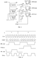
- FIG. 2 is a block diagram of programmable clock divider according to a presently disclosed embodiment.
- the programmable clock divider may be used to implement to the programmable clock divider 45 of the electronic system of FIG. 1 .
- the programmable clock divider of FIG. 2 may be implemented, for example, in a complementary metal-oxide semiconductor (CMOS) process.
- CMOS complementary metal-oxide semiconductor
- the programmable clock divider receives an input clock signal (CLKin) and a divide ratio signal (N) that indicates a divide ratio and produces an output clock signal (CLKdiv) that toggles at a frequency that is the frequency of the input clock signal divided by the divide ratio.
- CLKin input clock signal
- N divide ratio signal
- CLKdiv output clock signal
- a buffer 210 receives the input clock signal and produces buffered clock signals for use by other circuits in the programmable clock divider.
- the buffer 210 may produce a complementary pair of buffered clock signals.
- Complementary buffered clock signals may be referred to as a positive buffered clock signal (CLK) and a negative buffered clock signal (CLKbar).
- the buffer 210 may include gating circuits to disable the buffered clock signals, for example, in a low-power mode.
- a modulo N counter 220 produces a count signal (COUNT) that counts modulo N.
- the count signal may have a bit width according to a range of values of the divide ratio. In an example embodiment, the count signal is four bits wide.
- the modulo N counter 220 counts each cycle of the buffered clock signals. For example, the count signal may cycle from 1 to N repeatedly. Other count sequences (e.g., N-1 to 0) may also be used.
- the modulo value is specified by the divide ratio.
- a half-rate clock signal generator 230 produces three half-rate clock signals based on the count output from the modulo N counter 220 and the divide ratio. Operations of the half-rate clock signal generator 230 are timed by the buffered clock signals. The half-rate clock signals toggle at one-half the frequency of the output clock signal. The phases of the half-rate clock signals are timed so that pairs of the half-rate clock signals can be combined to produce the output clock signal.
- Different pairs of the half-rate clock signals are used for even and odd divide ratios.
- a first one of the half-rate clock signals (common half-rate clock signal HRCLKcom) is common to both even and odd divide ratios.
- a second one of the half-rate clock signals (even half-rate clock signal HRCLKeven) is used for even divide ratios.
- a third one of the half-rate clock signals (odd half-rate clock signal HRCLKodd) is used for odd divide ratios.
- a first exclusive OR gate 242 receives the common half-rate clock signal and the even half-rate clock signal and produces an even clock signal (CLKeven) that is used to produce the output clock signal when the divide ratio is even.
- a second exclusive OR gate 241 receives the common half-rate clock signal and the odd half-rate clock signal and produces an odd clock signal (CLKodd) that is used to produce the output clock signal when the divide ratio is odd.
- a selector 250 produces the output clock signal by selecting the even clock signal when the divide ratio is even and the odd clock signal when the divide ratio is odd.
- FIG. 4 is waveform diagram that illustrates operation of the programmable clock divider.
- the waveforms illustrate a divide ratio of three and a divide ratio of four.
- the waveforms of FIG. 4 are for circuit delays that are small (much less that the clock period) for clear illustration; however, actual circuit delays may be comparable to a clock period.
- quadrature timing relationships one-quarter period phase shift between the common half-rate clock signal and the even half-rate clock signal and between the common half-rate clock signal and the odd half-rate clock signal.
- the quadrature timing relationships provides 50% duty cycles on output clock signal for both even and odd divide ratios.
- the common half-rate clock signal and the even half-rate clock signal toggle on rising edges of the input clock signal and the odd half-rate clock signal toggles on falling edges of the input clock signal.
- the even half-rate clock signal is not used and its waveform may be chosen for convenient implementation.
- the odd half-rate clock signal is not used and its waveform may be chosen for convenient implementation.
- Delay from input clock signal to output clock signal does not depend on the value of the divide ratio. This can simplify timing closure and allow high frequency operation.
- FIG. 3 is block diagram of a half-rate clock signal generator according to a presently disclosed embodiment.
- the half-rate clock signal generator may be used to implement to the half-rate clock signal generator 230 of the programmable clock divider of FIG. 2 .
- the half-rate clock signal generator of FIG. 3 receives a count signal (COUNT), a divide ratio signal (N), and complementary buffered clock signals (CLK and CLKbar) and produces three half-rate clock signals: a common half-rate clock signal (HRCLKcom), an even half-rate clock signal (HRCLKeven), and an odd half-rate clock signal (HRCLKodd).
- the complementary buffered clock signals include a positive buffered clock signal (CLK) and a negative buffered clock signal (CLKbar).
- the half-rate clock signal generator can generate signals as illustrated in FIG. 4 .
- the three half-rate clock signals are supplied by three toggle flip-flops.
- a first toggle flip-flop 330 produces the common half-rate clock signal.
- a second toggle flip-flop 332 produces the even half-rate clock signal.
- a third toggle flip-flop 335 produces the odd half-rate clock signal.
- a first comparator 310 controls when the first toggle flip-flop 330, which produces the common half-rate clock signal, toggles.
- the first comparator 310 compares the value of the count signal to its starting value (1 for the waveforms illustrated is FIG. 4 ) and produces an active output when the values are equal.
- the output of the first comparator 310 is saved in a first pipeline flip-flop 320 on rising edges of the positive buffered clock signal.
- the first toggle flip-flop 330 is enabled by the output of the first pipeline flip-flop 320 and clocked by the positive buffered clock signal. The use of the pipeline flip-flop can improve setup and hold timing and thereby increase maximum operating frequency.
- a second comparator 312 controls when the second toggle flip-flop 332, which produces the even half-rate clock signal, toggles.
- the second comparator 312 compares the value of the count signal to its midpoint value and produces an active output when the values are equal.
- the midpoint value may be selected to be N/2+1 (3 for the divide ratio of 4 illustrated in FIG. 4 ) in the illustrated embodiment.
- the output of the second comparator 312 is saved in a second pipeline flip-flop 322 on rising edges of the positive buffered clock signal.
- the second toggle flip-flop 332 is enabled by the output of the second pipeline flip-flop 322 and clocked by the positive buffered clock signal.
- a third comparator 315 controls when the third toggle flip-flop 335, which produces the odd half-rate clock signal, toggles.
- the third comparator 315 compares the value of the count signal to its midpoint value and produces an active output when the values are equal.
- the midpoint value may be selected to be (N+1)/2+1 (3 for the divide ratio of 3 illustrated in FIG. 4 ) in the illustrated embodiment.
- the output of the third comparator 315 is saved in a third pipeline flip-flop 325 on rising edges of the positive buffered clock signal.
- the third toggle flip-flop 335 is enabled by the output of the third pipeline flip-flop 325 and clocked by the negative buffered clock signal.
- Use of the negative buffered clock signal to clock the third toggle flip-flop 335 delays the odd half-rate clock signal by one-half the period of the input clock signal so that when odd half-rate clock signal is exclusive ORed with the common half-rate clock signal, the resulting signal has a 50% duty cycle.
- the values used in the comparator are exemplary.
- the comparison values can be adjusted by corresponding amounts to produce clock signals with the same (but shifted with respect to the count signal) waveforms. Additionally, the comparison values can be adjusted when a different number of pipeline flip-flops are used.
- the programmable clock divider of FIG. 2 using the half-rate clock signal generator of FIG. 3 produces the output clock signal with the delay from the input clock signal to the output clock signal being independent of the divide ratio.
- This delay relationship may be referred to as constant delay.
- the delay may vary with operating conditions, for example, temperature and supply voltage, of the programmable clock divider.
- the delay from the input clock signal to the output clock signal includes delays in the clock buffer, the toggle flip-flops, the exclusive OR gates, and the selector. These delays may vary slightly, for example, the delay of the selector to its output may be different between the even clock signal and the odd clock signal. Such delay differences can be small, for example, less than the delay of one logic gate.
- the programmable clock divider of FIG. 2 using the half-rate clock signal generator of FIG. 3 can also operate at high frequency, for example, 3.5 GHz. Additionally, the output clock has a 50% duty cycle for all divide ratios. Similar to the constant delay, the duty cycle may vary slightly.
- FIG. 5 is a flowchart of a process for dividing a clock signal by a programmable integer value according to a presently disclosed embodiment.
- the process of FIG. 5 may be performed with any suitable circuit; however, to provide a specific example, the process will be described with reference to the programmable clock divider of FIG. 2 and half-rate clock signal generator of FIG. 3 .
- the process of FIG. 5 receives an input clock signal (CLKin) and a divide ratio signal (N) that indicates a divide ratio and produces an output clock signal (CLKdiv) that toggles at a frequency that is the frequency of the input clock signal divided by the divide ratio.
- CLKin an input clock signal
- N divide ratio signal
- CLKdiv output clock signal
- the process counts modulo N.
- the modulo N counter 220 may produce a count signal that counts modulo the divide ratio with the value of the count signal changing on transitions of the input clock signal.
- step 520 the process uses the count signal and divide ratio to produce a common half-rate clock signal, an even half-rate clock signal, and an odd half-rate clock signal that toggle at one-half the rate of the output clock signal.
- the half-rate clock signal generator of FIG. 3 can produce the three half-rate clock signals using toggle flip-flops that are enabled based on comparison of the value of the count signal starting and midpoint values of the count signal.
- the process uses the common half-rate clock signal, the even half-rate clock signal, and the odd half-rate clock signal to produce the output clock signal.
- the first exclusive OR gate 242 can combine the common half-rate clock signal and the even half-rate clock signal to produce the output clock signal when the divide ratio is even and the second exclusive OR gate 241 can combine the common half-rate clock signal and the odd half-rate clock signal to produce the output clock signal when the divide ratio is odd.
- FIG. 5 may be modified, for example, by adding or altering steps. Additionally, steps may be performed concurrently.
Description
- The present invention relates to electronic circuits and, more particularly, to programmable clock dividers.
- A programmable clock divider receives an input clock signal at an input frequency and produces an output clock signal at an output frequency with the ratio of the input frequency to the output frequency set by a programmable divide ratio. Programmable clock dividers are used in many electronic devices. For example, a programmable clock divider can be used to implement multiple frequencies of operation for a Display Serial Interface (DSI) link between a processor and a display device. DSI is an interface standard established by the Mobile Industry Processor Interface (MIPI) Alliance. The DSI link may operate at many different frequencies, for example, depending on characteristics of the display, with a clock signal toggling at the different frequencies produced by a programmable clock divider.
-
FIG. 1 is a block diagram of an electronic system that includes a programmable clock divider. The system includes aDSI interface 20. TheDSI interface 20 is coupled to DSI signals for communication with adisplay device 10. TheDSI interface 20 may receive data signals and format the signals for communication according to DSI specifications. TheDSI interface 20 receives a clock signal (CLKdiv) for use in performing its functions. - A
programmable clock divider 45 receives an input clock signal (CLKin) and produces an output clock signal (CLKdiv). Theprogrammable clock divider 45 receives a divide ratio signal (N) that indicates the ratio of the frequency of the input clock signal to the frequency of the output clock signal. - The system of
FIG. 1 also includes anSoC block 90. The SoCblock 90 provides other functions of the electronic system. TheSoC block 90 may supply data to theDSI interface 20. TheSoC block 90 may also supply the divide ratio signal and the input clock signal to theprogrammable clock divider 45. - The clock signal used by the DSI
interface 20 may toggle at a wide range of frequencies, for example, 2.5 GHz to 80 MHz. A programmable clock divider that can operate at such high frequencies may be difficult to implement. Additionally, the system may be improved when the delay of theprogrammable clock divider 45 from the input clock signal to the output clock signal is constant. For example, theSoC block 90 may time some operations using the input clock signal supplied to theprogrammable clock divider 45. The delay of the programmable clock divider 45 effects the timing of data signals between theSoC block 90 and theDSI interface 20. Thus, a constant delay ofprogrammable clock divider 45 may allow the system to operate at high frequencies. Additionally, functions of circuits in theDSI interface 20 may be improved when the duty cycle of the clock signal used is near 50%. Providing a 50% duty cycle output clock signal is more difficult when the divide ratio is an odd number. Thus, providing a programmable clock divider that produces an output clock signal with a 50% duty cycle, has a constant delay, and operates at high frequencies is valuable. - Many other systems use programmable clock dividers and may have similar requirements.
- Attention is drawn to the document
US 2008/0219399A1 , which describes an apparatus for dividing the frequency of an input signal by an integer N. First and second means may divide the frequency of the input signal by a factor of N and then by a factor of 2. An output of the first means and an output of the second means may be combined by an exclusive OR gate. Third means may be used to control the relative phase of the outputs from the first and second means such that the output from the first means and the output of the second means differ in phase by one-quarter cycle or 90 degrees. - In accordance with the present invention, a method and an apparatus, as set forth in the independent claims is provided. Embodiments of the invention are claimed in the dependent claims.
- In one aspect, a programmable clock divider is provided for receiving an input clock signal at an input frequency and producing an output clock signal at an output frequency, .the ratio of the input frequency to the output frequency set by a programmable divide ratio The programmable clock divider includes: a modulo N counter configured to produce a count signal that counts modulo the divide ratio; a half-rate clock signal generator configured to produce a common half-rate clock signal, an even half-rate clock signal, and an odd half-rate clock signal that toggle at one-half the rate of the output clock signal; a first exclusive OR gate having inputs coupled to the common half-rate clock signal and the even half-rate clock signal and an output driving an even clock signal; a second exclusive OR gate having inputs coupled the common half-rate clock signal and the odd half-rate clock signal and an output driving an even clock signal; and a selector configured to produce the output clock signal by selecting the even clock signal when the divide ratio is even and selecting the odd clock signal when the divide ratio is odd.
- In one aspect, a method is provided for dividing an input clock signal by a programmable divide ratio. The method includes: counting, on edges of the input clock signal, modulo the divide ratio to produce a count signal; producing, based on the count signal and the divide ratio, a common half-rate clock signal, an even half-rate clock signal, and an odd half-rate clock signal that toggle at one-half the rate of the output clock signal; and producing an output clock signal using on the common half-rate clock signal, the even half-rate clock signal, and the odd half-rate clock signal.
- In one aspect, an apparatus is provided for receiving an input clock signal at an input frequency and producing an output clock signal at an output frequency, the ratio of the input frequency to the output frequency set by a programmable divide ratio. The apparatus includes: counting, on edges of the input clock signal, modulo the divide ratio to produce a count signal; producing, based on the count signal and the divide ratio, a common half-rate clock signal, an even half-rate clock signal, and an odd half-rate clock signal that toggle at one-half the rate of the output clock signal; and producing an output clock signal using on the common half-rate clock signal, the even half-rate clock signal, and the odd half-rate clock signal.
- Other features and advantages of the present invention should be apparent from the following description which illustrates, by way of example, aspects of the invention.
- The details of the present invention, both as to its structure and operation, may be gleaned in part by study of the accompanying drawings, in which like reference numerals refer to like parts, and in which:
-
FIG. 1 is a block diagram of an electronic system that includes a programmable clock divider; -
FIG. 2 is a block diagram of programmable clock divider according to a presently disclosed embodiment; -
FIG. 3 is block diagram of a half-rate clock signal generator according to a presently disclosed embodiment; -
FIG. 4 is a waveform diagram illustrate operation of a programmable clock divider according to a presently disclosed embodiment; and -
FIG. 5 is a flowchart of a process for dividing a clock signal by a programmable integer value according to a presently disclosed embodiment. - The detailed description set forth below, in connection with the accompanying drawings, is intended as a description of various configurations and is not intended to represent the only configurations in which the concepts described herein may be practiced. The detailed description includes specific details for the purpose of providing a thorough understanding of the various concepts. However, it will be apparent to those skilled in the art that these concepts may be practiced without these specific details. In some instances, well-known structures and components are shown in simplified form in order to avoid obscuring such concepts.
-
FIG. 2 is a block diagram of programmable clock divider according to a presently disclosed embodiment. The programmable clock divider may be used to implement to theprogrammable clock divider 45 of the electronic system ofFIG. 1 . The programmable clock divider ofFIG. 2 may be implemented, for example, in a complementary metal-oxide semiconductor (CMOS) process. The programmable clock divider receives an input clock signal (CLKin) and a divide ratio signal (N) that indicates a divide ratio and produces an output clock signal (CLKdiv) that toggles at a frequency that is the frequency of the input clock signal divided by the divide ratio. - A
buffer 210 receives the input clock signal and produces buffered clock signals for use by other circuits in the programmable clock divider. Thebuffer 210 may produce a complementary pair of buffered clock signals. Complementary buffered clock signals may be referred to as a positive buffered clock signal (CLK) and a negative buffered clock signal (CLKbar). In addition to buffering, thebuffer 210 may include gating circuits to disable the buffered clock signals, for example, in a low-power mode. - A
modulo N counter 220 produces a count signal (COUNT) that counts modulo N. The count signal may have a bit width according to a range of values of the divide ratio. In an example embodiment, the count signal is four bits wide. Themodulo N counter 220 counts each cycle of the buffered clock signals. For example, the count signal may cycle from 1 to N repeatedly. Other count sequences (e.g., N-1 to 0) may also be used. The modulo value is specified by the divide ratio. - A half-rate
clock signal generator 230 produces three half-rate clock signals based on the count output from the modulo N counter 220 and the divide ratio. Operations of the half-rateclock signal generator 230 are timed by the buffered clock signals. The half-rate clock signals toggle at one-half the frequency of the output clock signal. The phases of the half-rate clock signals are timed so that pairs of the half-rate clock signals can be combined to produce the output clock signal. - Different pairs of the half-rate clock signals are used for even and odd divide ratios. A first one of the half-rate clock signals (common half-rate clock signal HRCLKcom) is common to both even and odd divide ratios. A second one of the half-rate clock signals (even half-rate clock signal HRCLKeven) is used for even divide ratios. A third one of the half-rate clock signals (odd half-rate clock signal HRCLKodd) is used for odd divide ratios.
- The pairs of the half-rate clock signals are exclusive ORed to produce the output clock signal. A first exclusive OR
gate 242 receives the common half-rate clock signal and the even half-rate clock signal and produces an even clock signal (CLKeven) that is used to produce the output clock signal when the divide ratio is even. A second exclusive ORgate 241 receives the common half-rate clock signal and the odd half-rate clock signal and produces an odd clock signal (CLKodd) that is used to produce the output clock signal when the divide ratio is odd. - A
selector 250 produces the output clock signal by selecting the even clock signal when the divide ratio is even and the odd clock signal when the divide ratio is odd. -
FIG. 4 is waveform diagram that illustrates operation of the programmable clock divider. The waveforms illustrate a divide ratio of three and a divide ratio of four. The waveforms ofFIG. 4 are for circuit delays that are small (much less that the clock period) for clear illustration; however, actual circuit delays may be comparable to a clock period. - As shown, there are quadrature timing relationships (one-quarter period phase shift) between the common half-rate clock signal and the even half-rate clock signal and between the common half-rate clock signal and the odd half-rate clock signal. The quadrature timing relationships provides 50% duty cycles on output clock signal for both even and odd divide ratios. To achieve the quadrature timing relationships, the common half-rate clock signal and the even half-rate clock signal toggle on rising edges of the input clock signal and the odd half-rate clock signal toggles on falling edges of the input clock signal.
- For odd divide ratios, the even half-rate clock signal is not used and its waveform may be chosen for convenient implementation. Similarly, for even divide ratios, the odd half-rate clock signal is not used and its waveform may be chosen for convenient implementation.
- Delay from input clock signal to output clock signal does not depend on the value of the divide ratio. This can simplify timing closure and allow high frequency operation.
-
FIG. 3 is block diagram of a half-rate clock signal generator according to a presently disclosed embodiment. The half-rate clock signal generator may be used to implement to the half-rateclock signal generator 230 of the programmable clock divider ofFIG. 2 . The half-rate clock signal generator ofFIG. 3 receives a count signal (COUNT), a divide ratio signal (N), and complementary buffered clock signals (CLK and CLKbar) and produces three half-rate clock signals: a common half-rate clock signal (HRCLKcom), an even half-rate clock signal (HRCLKeven), and an odd half-rate clock signal (HRCLKodd). The complementary buffered clock signals include a positive buffered clock signal (CLK) and a negative buffered clock signal (CLKbar). The half-rate clock signal generator can generate signals as illustrated inFIG. 4 . - The three half-rate clock signals are supplied by three toggle flip-flops. A first toggle flip-
flop 330 produces the common half-rate clock signal. A second toggle flip-flop 332 produces the even half-rate clock signal. A third toggle flip-flop 335 produces the odd half-rate clock signal. When the toggle flip-flops toggle is determined from the count signal and the divide ratio. The count signal is compared to values derived from the divide ratio to control when the toggle flip-flops toggle. - A
first comparator 310 controls when the first toggle flip-flop 330, which produces the common half-rate clock signal, toggles. Thefirst comparator 310 compares the value of the count signal to its starting value (1 for the waveforms illustrated isFIG. 4 ) and produces an active output when the values are equal. The output of thefirst comparator 310 is saved in a first pipeline flip-flop 320 on rising edges of the positive buffered clock signal. The first toggle flip-flop 330 is enabled by the output of the first pipeline flip-flop 320 and clocked by the positive buffered clock signal. The use of the pipeline flip-flop can improve setup and hold timing and thereby increase maximum operating frequency. - A
second comparator 312 controls when the second toggle flip-flop 332, which produces the even half-rate clock signal, toggles. Thesecond comparator 312 compares the value of the count signal to its midpoint value and produces an active output when the values are equal. The midpoint value may be selected to be N/2+1 (3 for the divide ratio of 4 illustrated inFIG. 4 ) in the illustrated embodiment. The output of thesecond comparator 312 is saved in a second pipeline flip-flop 322 on rising edges of the positive buffered clock signal. The second toggle flip-flop 332 is enabled by the output of the second pipeline flip-flop 322 and clocked by the positive buffered clock signal. - A
third comparator 315 controls when the third toggle flip-flop 335, which produces the odd half-rate clock signal, toggles. Thethird comparator 315 compares the value of the count signal to its midpoint value and produces an active output when the values are equal. The midpoint value may be selected to be (N+1)/2+1 (3 for the divide ratio of 3 illustrated inFIG. 4 ) in the illustrated embodiment. The output of thethird comparator 315 is saved in a third pipeline flip-flop 325 on rising edges of the positive buffered clock signal. The third toggle flip-flop 335 is enabled by the output of the third pipeline flip-flop 325 and clocked by the negative buffered clock signal. Use of the negative buffered clock signal to clock the third toggle flip-flop 335 delays the odd half-rate clock signal by one-half the period of the input clock signal so that when odd half-rate clock signal is exclusive ORed with the common half-rate clock signal, the resulting signal has a 50% duty cycle. - The values used in the comparator are exemplary. The comparison values can be adjusted by corresponding amounts to produce clock signals with the same (but shifted with respect to the count signal) waveforms. Additionally, the comparison values can be adjusted when a different number of pipeline flip-flops are used.
- The programmable clock divider of
FIG. 2 using the half-rate clock signal generator ofFIG. 3 produces the output clock signal with the delay from the input clock signal to the output clock signal being independent of the divide ratio. This delay relationship may be referred to as constant delay. However, the delay may vary with operating conditions, for example, temperature and supply voltage, of the programmable clock divider. The delay from the input clock signal to the output clock signal includes delays in the clock buffer, the toggle flip-flops, the exclusive OR gates, and the selector. These delays may vary slightly, for example, the delay of the selector to its output may be different between the even clock signal and the odd clock signal. Such delay differences can be small, for example, less than the delay of one logic gate. - The programmable clock divider of
FIG. 2 using the half-rate clock signal generator ofFIG. 3 can also operate at high frequency, for example, 3.5 GHz. Additionally, the output clock has a 50% duty cycle for all divide ratios. Similar to the constant delay, the duty cycle may vary slightly. -
FIG. 5 is a flowchart of a process for dividing a clock signal by a programmable integer value according to a presently disclosed embodiment. The process ofFIG. 5 may be performed with any suitable circuit; however, to provide a specific example, the process will be described with reference to the programmable clock divider ofFIG. 2 and half-rate clock signal generator ofFIG. 3 . The process ofFIG. 5 receives an input clock signal (CLKin) and a divide ratio signal (N) that indicates a divide ratio and produces an output clock signal (CLKdiv) that toggles at a frequency that is the frequency of the input clock signal divided by the divide ratio. - In
step 510, the process counts modulo N. For example, the modulo N counter 220 may produce a count signal that counts modulo the divide ratio with the value of the count signal changing on transitions of the input clock signal. - In
step 520, the process uses the count signal and divide ratio to produce a common half-rate clock signal, an even half-rate clock signal, and an odd half-rate clock signal that toggle at one-half the rate of the output clock signal. For example, the half-rate clock signal generator ofFIG. 3 can produce the three half-rate clock signals using toggle flip-flops that are enabled based on comparison of the value of the count signal starting and midpoint values of the count signal. - In
step 530, the process uses the common half-rate clock signal, the even half-rate clock signal, and the odd half-rate clock signal to produce the output clock signal. For example, the first exclusive ORgate 242 can combine the common half-rate clock signal and the even half-rate clock signal to produce the output clock signal when the divide ratio is even and the second exclusive ORgate 241 can combine the common half-rate clock signal and the odd half-rate clock signal to produce the output clock signal when the divide ratio is odd. - The process of
FIG. 5 may be modified, for example, by adding or altering steps. Additionally, steps may be performed concurrently. - Although particular embodiments are described above, many variations are possible, including, for example, those with different signal polarities. Additionally, signal buffers and pipeline stages may be added, moved, or deleted. Furthermore, functions described as be performed by one block may be moved to another block or distributed across blocks. Additionally, features of the various embodiments may be combined in combinations that differ from those described above.
- The above description of the disclosed embodiments is provided to enable any person skilled in the art to make or use the invention. Various modifications to these embodiments will be readily apparent to those skilled in the art, and the generic principles described herein can be applied to other embodiments without departing from the scope of the invention as defined in the appended claims. Thus, it is to be understood that the description and drawings presented herein represent presently preferred embodiments of the invention and are therefore representative of the subject matter which is broadly contemplated by the present invention. It is further understood that the scope of the present invention fully encompasses other embodiments that may become obvious to those skilled in the art and that the scope of the present invention is accordingly limited by nothing other than the appended claims.
Claims (13)
- A method for dividing an input clock signal by a programmable divide ratio, the method comprising:Counting (510), on edges of the input clock signal, modulo the programmable divide ratio to produce a count signal;Producing (520), based on the count signal and the programmable divide ratio, a common half-rate clock signal, an even half-rate clock signal, and an odd half-rate clock signal that each toggle at one-half the rate of the output clock signal; andcombining (530) the common half-rate clock signal and the even half-rate clock signal to produce an even clock signal;combining (530) the common half-rate clock signal and the odd half-rate clock signal to produce an odd clock signal; andselecting as an output clock signal, the even clock signal when the programmable divide ratio is even and selecting, as the output clock signal, the odd clock signal when the programmable divide ratio is odd.
- The method of claim 1, wherein the delay from the input clock signal to the output clock signal is independent of the value of the programmable divide ratio.
- The method of claim 1, wherein the duty cycle of the output clock signal is 50% independent of the value of the programmable divide ratio.
- The method of claim 1, wherein the common half-rate clock signal and the even half-rate clock have quadrature timing relationship for even divide ratios, and the common half-rate clock signal and the odd half-rate clock have quadrature timing relationship for odd divide ratios.
- The method of claim 1, wherein:the common half-rate clock signal transitions at rising edges of the input clock signal;the even half-rate clock signal transitions at rising edges of the input clock signal; andthe odd half-rate clock signal transitions at falling edges of the input clock signal.
- The method of claim 1, wherein:the common half-rate clock signal transitions after the count signal equals a starting value of the count signal;the even half-rate clock signal transitions after the count signal equals an even midpoint value of the count signal; andthe odd half-rate clock signal transitions after the count signal equals an odd midpoint value of the count signal.
- An apparatus (45) for receiving an input clock signal at an input frequency and producing an output clock signal at an output frequency, the ratio of the input frequency to the output frequency set by a programmable divide ratio, the apparatus comprising:a modulo N counter means (220) for producing a count signal that counts modulo the programmable divide ratio;a half-rate clock signal generator means (230) for producing a common half-rate clock signal toggling on rising edges of the input clock signal, an even half-rate clock signal toggling on the rising edges of the input clock signal, and an odd half-rate clock signal toggling on the falling edges of the input clock signal, the half-rate clock signals toggling at one-half the rate of the output clock signal;a first exclusive OR gate (242) having inputs coupled to the common half-rate clock signal and the even half-rate clock signal and an output driving an even clock signal;a second exclusive OR gate (241) having inputs coupled the common half-rate clock signal and the odd half-rate clock signal and an output driving an odd clock signal; anda selector (250) configured to produce the output clock signal by selecting the even clock signal when the programmable divide ratio is even and selecting the odd clock signal when the programmable divide ratio is odd.
- The apparatus (45) of claim 7, wherein the delay from the input clock signal to the output clock signal is independent of the value of the programmable divide ratio.
- The apparatus (45) of claim 7, wherein the duty cycle of the output clock signal is 50% independent of the value of the programmable divide ratio.
- The apparatus (45) of claim 7, wherein the common half-rate clock signal and the even half-rate clock have quadrature timing relationship for even divide ratios, and the common half-rate clock signal and the odd half-rate clock have quadrature timing relationship for odd divide ratios.
- The apparatus (45) of claim 7, wherein the half-rate clock signal generator (230) comprises:a first toggle flip-flop (330) clocked on the rising edges of the input clock signal and configured to produce the common half-rate clock signal;a second toggle flip-flop (332) clocked on rising edges of the input clock signal and configured to produce the even half-rate clock signal; anda third toggle flip-flop (335) clocked on falling edges of the input clock signal and configured to produce the odd half-rate clock signal.
- The apparatus (45) of claim 11, wherein the half-rate clock signal generator further comprises:a first comparator (310) configured to compare the value of the count signal to a starting value of the count signal and produce an enable for the first toggle flip-flop based on the comparison;a second comparator (312) configured to compare the value of the count signal to an even midpoint value of the count signal and produce an enable for the second toggle flip-flop based on the comparison; anda third comparator (315) configured to compare the value of the count signal to an odd midpoint value of the count signal and produce an enable for the third toggle flip-flop based on the comparison.
- The apparatus (45) of claim 12, wherein the half-rate clock signal generator (230) further comprises:a first pipeline flip-flop (320) coupled between the first comparator and the first toggle flip-flop;a second pipeline flip-flop (322) coupled between the second comparator and the second toggle flip-flop; anda third pipeline flip-flop (325) coupled between the third comparator and the third toggle flip-flop.
Applications Claiming Priority (2)
| Application Number | Priority Date | Filing Date | Title |
|---|---|---|---|
| US14/855,238 US9762228B2 (en) | 2015-09-15 | 2015-09-15 | High-speed programmable clock divider |
| PCT/US2016/046333 WO2017048419A1 (en) | 2015-09-15 | 2016-08-10 | High-speed programmable clock divider |
Publications (2)
| Publication Number | Publication Date |
|---|---|
| EP3350928A1 EP3350928A1 (en) | 2018-07-25 |
| EP3350928B1 true EP3350928B1 (en) | 2019-01-09 |
Family
ID=56741189
Family Applications (1)
| Application Number | Title | Priority Date | Filing Date |
|---|---|---|---|
| EP16754368.5A Active EP3350928B1 (en) | 2015-09-15 | 2016-08-10 | High-speed programmable clock divider |
Country Status (9)
| Country | Link |
|---|---|
| US (1) | US9762228B2 (en) |
| EP (1) | EP3350928B1 (en) |
| JP (1) | JP6483329B2 (en) |
| KR (1) | KR101923012B1 (en) |
| CN (1) | CN108028656B (en) |
| BR (1) | BR112018005030B1 (en) |
| ES (1) | ES2715029T3 (en) |
| HU (1) | HUE043658T2 (en) |
| WO (1) | WO2017048419A1 (en) |
Families Citing this family (3)
| Publication number | Priority date | Publication date | Assignee | Title |
|---|---|---|---|---|
| US10063234B1 (en) * | 2017-07-13 | 2018-08-28 | Micron Technology, Inc. | Half-frequency command path |
| US11038666B1 (en) | 2019-12-11 | 2021-06-15 | Qualcomm Incorporated | Open-loop, super fast, half-rate clock and data recovery for next generation C-PHY interfaces |
| US11874693B2 (en) | 2022-05-24 | 2024-01-16 | Analog Devices International Unlimited Company | Reconfigurable clock divider |
Family Cites Families (21)
| Publication number | Priority date | Publication date | Assignee | Title |
|---|---|---|---|---|
| US4623846A (en) * | 1985-02-14 | 1986-11-18 | Motorola, Inc. | Constant duty cycle, frequency programmable clock generator |
| US5362119A (en) * | 1993-09-29 | 1994-11-08 | Rosentratter Billy F | Glare shield |
| US5524035A (en) * | 1995-08-10 | 1996-06-04 | International Business Machines Corporation | Symmetric clock system for a data processing system including dynamically switchable frequency divider |
| DE69614821T2 (en) * | 1996-01-19 | 2002-01-17 | St Microelectronics Srl | Switched clock |
| JP3159238B2 (en) * | 1996-09-17 | 2001-04-23 | 日本電気株式会社 | Numerically controlled oscillator |
| EP1241788A1 (en) * | 2001-03-13 | 2002-09-18 | STMicroelectronics Limited | Digital frequency divider |
| JP3949995B2 (en) * | 2001-12-28 | 2007-07-25 | シャープ株式会社 | Counter circuit |
| US7358782B2 (en) * | 2005-08-17 | 2008-04-15 | Broadcom Corporation | Frequency divider and associated methods |
| US20080219399A1 (en) | 2007-03-07 | 2008-09-11 | Nary Kevin R | Frequency Divider With Symmetrical Output |
| AU2009266952B2 (en) * | 2008-07-01 | 2013-05-16 | Proterra Operating Company, Inc. | Charging stations for electric vehicles |
| US7881422B1 (en) * | 2008-07-10 | 2011-02-01 | Marvell International Ltd. | Circuits and methods for dividing frequency by an odd value |
| US8368436B1 (en) | 2010-10-29 | 2013-02-05 | Maxim Integrated, Inc. | Programmable frequency synthesizer with I/Q outputs |
| CN102055465A (en) * | 2010-12-09 | 2011-05-11 | 山东大学 | Frequency divider capable of configuring any integer and half-integer and method using same |
| US8471608B2 (en) | 2011-02-02 | 2013-06-25 | Texas Instruments Incorporated | Clock divider circuit |
| US8378719B1 (en) | 2011-10-18 | 2013-02-19 | St-Ericsson Sa | Programmable high-speed frequency divider |
| US8558575B1 (en) * | 2012-03-23 | 2013-10-15 | Applied Micro Circuits Corporation | Clock generation for N.5 modulus divider |
| US8744037B2 (en) | 2012-06-11 | 2014-06-03 | Intel Mobil Communications GmbH | Divider, method for providing an output signal and edge tracker |
| EP2806562A1 (en) | 2013-05-22 | 2014-11-26 | Asahi Kasei Microdevices Corporation | Programmable frequency divider module with duty cycle close to fifty percent |
| US10579580B2 (en) * | 2013-12-18 | 2020-03-03 | Qorvo Us, Inc. | Start of sequence detection for one wire bus |
| US8829953B1 (en) | 2014-01-09 | 2014-09-09 | Freescale Semiconductor, Inc. | Programmable clock divider |
| CN104682954B (en) * | 2015-02-06 | 2017-07-18 | 北京大学 | A kind of half rate random data phase detecting circuit |
-
2015
- 2015-09-15 US US14/855,238 patent/US9762228B2/en active Active
-
2016
- 2016-08-10 WO PCT/US2016/046333 patent/WO2017048419A1/en active Application Filing
- 2016-08-10 BR BR112018005030-0A patent/BR112018005030B1/en active IP Right Grant
- 2016-08-10 JP JP2018513481A patent/JP6483329B2/en active Active
- 2016-08-10 HU HUE16754368A patent/HUE043658T2/en unknown
- 2016-08-10 EP EP16754368.5A patent/EP3350928B1/en active Active
- 2016-08-10 KR KR1020187010466A patent/KR101923012B1/en active IP Right Grant
- 2016-08-10 ES ES16754368T patent/ES2715029T3/en active Active
- 2016-08-10 CN CN201680053366.2A patent/CN108028656B/en active Active
Non-Patent Citations (1)
| Title |
|---|
| None * |
Also Published As
| Publication number | Publication date |
|---|---|
| CN108028656A (en) | 2018-05-11 |
| HUE043658T2 (en) | 2019-08-28 |
| EP3350928A1 (en) | 2018-07-25 |
| US9762228B2 (en) | 2017-09-12 |
| WO2017048419A1 (en) | 2017-03-23 |
| BR112018005030B1 (en) | 2023-04-18 |
| JP6483329B2 (en) | 2019-03-13 |
| US20170077918A1 (en) | 2017-03-16 |
| JP2018526940A (en) | 2018-09-13 |
| BR112018005030A2 (en) | 2018-10-02 |
| KR20180043380A (en) | 2018-04-27 |
| CN108028656B (en) | 2019-05-31 |
| KR101923012B1 (en) | 2018-11-28 |
| ES2715029T3 (en) | 2019-05-31 |
Similar Documents
| Publication | Publication Date | Title |
|---|---|---|
| US10181844B1 (en) | Clock duty cycle calibration and frequency multiplier circuit | |
| US7777534B2 (en) | Fraction-N frequency divider and method thereof | |
| US8686764B2 (en) | Edge selection techniques for correcting clock duty cycle | |
| US20080219399A1 (en) | Frequency Divider With Symmetrical Output | |
| US8471607B1 (en) | High-speed frequency divider architecture | |
| US8278987B2 (en) | Duty cycle based phase interpolators and methods for use | |
| CN103929173A (en) | Frequency divider and wireless communication device | |
| TWI652902B (en) | Quadrature clock generating apparatus and communication system transmitter | |
| US8829953B1 (en) | Programmable clock divider | |
| US10476707B2 (en) | Hybrid half/quarter-rate DFE | |
| EP3350928B1 (en) | High-speed programmable clock divider | |
| US8406371B1 (en) | Programmable divider circuitry for improved duty cycle consistency and related systems and methods | |
| US7342425B1 (en) | Method and apparatus for a symmetrical odd-number clock divider | |
| TWI569582B (en) | Apparatus and method for clock data recovery and phase detector | |
| US6956922B2 (en) | Generating non-integer clock division | |
| US8319532B2 (en) | Frequency divider with phase selection functionality | |
| US9966964B1 (en) | Multi-phase divider | |
| CN104821808A (en) | Phase interpolator | |
| TW201515397A (en) | Oscillator | |
| EP2256932A1 (en) | Circuit for aligning clock to parallel data | |
| US7253673B2 (en) | Multi-phase clock generator and generating method for network controller | |
| KR20150090861A (en) | Clock divider | |
| CN109217869A (en) | PLL phase rotator system and method |
Legal Events
| Date | Code | Title | Description |
|---|---|---|---|
| STAA | Information on the status of an ep patent application or granted ep patent |
Free format text: STATUS: THE INTERNATIONAL PUBLICATION HAS BEEN MADE |
|
| PUAI | Public reference made under article 153(3) epc to a published international application that has entered the european phase |
Free format text: ORIGINAL CODE: 0009012 |
|
| STAA | Information on the status of an ep patent application or granted ep patent |
Free format text: STATUS: REQUEST FOR EXAMINATION WAS MADE |
|
| REG | Reference to a national code |
Ref country code: DE Ref legal event code: R079 Ref document number: 602016009278 Country of ref document: DE Free format text: PREVIOUS MAIN CLASS: H03K0021100000 Ipc: G06F0001080000 |
|
| 17P | Request for examination filed |
Effective date: 20180328 |
|
| AK | Designated contracting states |
Kind code of ref document: A1 Designated state(s): AL AT BE BG CH CY CZ DE DK EE ES FI FR GB GR HR HU IE IS IT LI LT LU LV MC MK MT NL NO PL PT RO RS SE SI SK SM TR |
|
| AX | Request for extension of the european patent |
Extension state: BA ME |
|
| GRAP | Despatch of communication of intention to grant a patent |
Free format text: ORIGINAL CODE: EPIDOSNIGR1 |
|
| STAA | Information on the status of an ep patent application or granted ep patent |
Free format text: STATUS: GRANT OF PATENT IS INTENDED |
|
| RIC1 | Information provided on ipc code assigned before grant |
Ipc: H03K 23/00 20060101ALI20180719BHEP Ipc: H03K 19/21 20060101ALI20180719BHEP Ipc: G06F 1/08 20060101AFI20180719BHEP Ipc: H03K 7/06 20060101ALI20180719BHEP Ipc: H03K 21/00 20060101ALI20180719BHEP Ipc: H03K 23/64 20060101ALI20180719BHEP Ipc: H03K 3/037 20060101ALI20180719BHEP Ipc: H03K 21/02 20060101ALI20180719BHEP Ipc: H03K 21/10 20060101ALI20180719BHEP |
|
| DAV | Request for validation of the european patent (deleted) | ||
| DAX | Request for extension of the european patent (deleted) | ||
| INTG | Intention to grant announced |
Effective date: 20180807 |
|
| GRAS | Grant fee paid |
Free format text: ORIGINAL CODE: EPIDOSNIGR3 |
|
| GRAA | (expected) grant |
Free format text: ORIGINAL CODE: 0009210 |
|
| STAA | Information on the status of an ep patent application or granted ep patent |
Free format text: STATUS: THE PATENT HAS BEEN GRANTED |
|
| AK | Designated contracting states |
Kind code of ref document: B1 Designated state(s): AL AT BE BG CH CY CZ DE DK EE ES FI FR GB GR HR HU IE IS IT LI LT LU LV MC MK MT NL NO PL PT RO RS SE SI SK SM TR |
|
| REG | Reference to a national code |
Ref country code: GB Ref legal event code: FG4D |
|
| REG | Reference to a national code |
Ref country code: CH Ref legal event code: EP Ref country code: AT Ref legal event code: REF Ref document number: 1088077 Country of ref document: AT Kind code of ref document: T Effective date: 20190115 |
|
| REG | Reference to a national code |
Ref country code: IE Ref legal event code: FG4D |
|
| REG | Reference to a national code |
Ref country code: DE Ref legal event code: R096 Ref document number: 602016009278 Country of ref document: DE |
|
| REG | Reference to a national code |
Ref country code: NL Ref legal event code: FP |
|
| REG | Reference to a national code |
Ref country code: LT Ref legal event code: MG4D |
|
| REG | Reference to a national code |
Ref country code: AT Ref legal event code: MK05 Ref document number: 1088077 Country of ref document: AT Kind code of ref document: T Effective date: 20190109 |
|
| PG25 | Lapsed in a contracting state [announced via postgrant information from national office to epo] |
Ref country code: SE Free format text: LAPSE BECAUSE OF FAILURE TO SUBMIT A TRANSLATION OF THE DESCRIPTION OR TO PAY THE FEE WITHIN THE PRESCRIBED TIME-LIMIT Effective date: 20190109 Ref country code: PT Free format text: LAPSE BECAUSE OF FAILURE TO SUBMIT A TRANSLATION OF THE DESCRIPTION OR TO PAY THE FEE WITHIN THE PRESCRIBED TIME-LIMIT Effective date: 20190509 Ref country code: LT Free format text: LAPSE BECAUSE OF FAILURE TO SUBMIT A TRANSLATION OF THE DESCRIPTION OR TO PAY THE FEE WITHIN THE PRESCRIBED TIME-LIMIT Effective date: 20190109 Ref country code: PL Free format text: LAPSE BECAUSE OF FAILURE TO SUBMIT A TRANSLATION OF THE DESCRIPTION OR TO PAY THE FEE WITHIN THE PRESCRIBED TIME-LIMIT Effective date: 20190109 Ref country code: NO Free format text: LAPSE BECAUSE OF FAILURE TO SUBMIT A TRANSLATION OF THE DESCRIPTION OR TO PAY THE FEE WITHIN THE PRESCRIBED TIME-LIMIT Effective date: 20190409 |
|
| REG | Reference to a national code |
Ref country code: HU Ref legal event code: AG4A Ref document number: E043658 Country of ref document: HU |
|
| PG25 | Lapsed in a contracting state [announced via postgrant information from national office to epo] |
Ref country code: IS Free format text: LAPSE BECAUSE OF FAILURE TO SUBMIT A TRANSLATION OF THE DESCRIPTION OR TO PAY THE FEE WITHIN THE PRESCRIBED TIME-LIMIT Effective date: 20190509 Ref country code: BG Free format text: LAPSE BECAUSE OF FAILURE TO SUBMIT A TRANSLATION OF THE DESCRIPTION OR TO PAY THE FEE WITHIN THE PRESCRIBED TIME-LIMIT Effective date: 20190409 Ref country code: GR Free format text: LAPSE BECAUSE OF FAILURE TO SUBMIT A TRANSLATION OF THE DESCRIPTION OR TO PAY THE FEE WITHIN THE PRESCRIBED TIME-LIMIT Effective date: 20190410 Ref country code: RS Free format text: LAPSE BECAUSE OF FAILURE TO SUBMIT A TRANSLATION OF THE DESCRIPTION OR TO PAY THE FEE WITHIN THE PRESCRIBED TIME-LIMIT Effective date: 20190109 Ref country code: LV Free format text: LAPSE BECAUSE OF FAILURE TO SUBMIT A TRANSLATION OF THE DESCRIPTION OR TO PAY THE FEE WITHIN THE PRESCRIBED TIME-LIMIT Effective date: 20190109 Ref country code: HR Free format text: LAPSE BECAUSE OF FAILURE TO SUBMIT A TRANSLATION OF THE DESCRIPTION OR TO PAY THE FEE WITHIN THE PRESCRIBED TIME-LIMIT Effective date: 20190109 |
|
| REG | Reference to a national code |
Ref country code: DE Ref legal event code: R097 Ref document number: 602016009278 Country of ref document: DE |
|
| PG25 | Lapsed in a contracting state [announced via postgrant information from national office to epo] |
Ref country code: SK Free format text: LAPSE BECAUSE OF FAILURE TO SUBMIT A TRANSLATION OF THE DESCRIPTION OR TO PAY THE FEE WITHIN THE PRESCRIBED TIME-LIMIT Effective date: 20190109 Ref country code: AL Free format text: LAPSE BECAUSE OF FAILURE TO SUBMIT A TRANSLATION OF THE DESCRIPTION OR TO PAY THE FEE WITHIN THE PRESCRIBED TIME-LIMIT Effective date: 20190109 Ref country code: EE Free format text: LAPSE BECAUSE OF FAILURE TO SUBMIT A TRANSLATION OF THE DESCRIPTION OR TO PAY THE FEE WITHIN THE PRESCRIBED TIME-LIMIT Effective date: 20190109 Ref country code: AT Free format text: LAPSE BECAUSE OF FAILURE TO SUBMIT A TRANSLATION OF THE DESCRIPTION OR TO PAY THE FEE WITHIN THE PRESCRIBED TIME-LIMIT Effective date: 20190109 Ref country code: DK Free format text: LAPSE BECAUSE OF FAILURE TO SUBMIT A TRANSLATION OF THE DESCRIPTION OR TO PAY THE FEE WITHIN THE PRESCRIBED TIME-LIMIT Effective date: 20190109 Ref country code: CZ Free format text: LAPSE BECAUSE OF FAILURE TO SUBMIT A TRANSLATION OF THE DESCRIPTION OR TO PAY THE FEE WITHIN THE PRESCRIBED TIME-LIMIT Effective date: 20190109 Ref country code: RO Free format text: LAPSE BECAUSE OF FAILURE TO SUBMIT A TRANSLATION OF THE DESCRIPTION OR TO PAY THE FEE WITHIN THE PRESCRIBED TIME-LIMIT Effective date: 20190109 |
|
| PLBE | No opposition filed within time limit |
Free format text: ORIGINAL CODE: 0009261 |
|
| STAA | Information on the status of an ep patent application or granted ep patent |
Free format text: STATUS: NO OPPOSITION FILED WITHIN TIME LIMIT |
|
| 26N | No opposition filed |
Effective date: 20191010 |
|
| PG25 | Lapsed in a contracting state [announced via postgrant information from national office to epo] |
Ref country code: TR Free format text: LAPSE BECAUSE OF FAILURE TO SUBMIT A TRANSLATION OF THE DESCRIPTION OR TO PAY THE FEE WITHIN THE PRESCRIBED TIME-LIMIT Effective date: 20190109 |
|
| PG25 | Lapsed in a contracting state [announced via postgrant information from national office to epo] |
Ref country code: MC Free format text: LAPSE BECAUSE OF FAILURE TO SUBMIT A TRANSLATION OF THE DESCRIPTION OR TO PAY THE FEE WITHIN THE PRESCRIBED TIME-LIMIT Effective date: 20190109 Ref country code: LU Free format text: LAPSE BECAUSE OF NON-PAYMENT OF DUE FEES Effective date: 20190810 Ref country code: LI Free format text: LAPSE BECAUSE OF NON-PAYMENT OF DUE FEES Effective date: 20190831 Ref country code: CH Free format text: LAPSE BECAUSE OF NON-PAYMENT OF DUE FEES Effective date: 20190831 |
|
| REG | Reference to a national code |
Ref country code: BE Ref legal event code: MM Effective date: 20190831 |
|
| PG25 | Lapsed in a contracting state [announced via postgrant information from national office to epo] |
Ref country code: IE Free format text: LAPSE BECAUSE OF NON-PAYMENT OF DUE FEES Effective date: 20190810 |
|
| PG25 | Lapsed in a contracting state [announced via postgrant information from national office to epo] |
Ref country code: BE Free format text: LAPSE BECAUSE OF NON-PAYMENT OF DUE FEES Effective date: 20190831 |
|
| PG25 | Lapsed in a contracting state [announced via postgrant information from national office to epo] |
Ref country code: CY Free format text: LAPSE BECAUSE OF FAILURE TO SUBMIT A TRANSLATION OF THE DESCRIPTION OR TO PAY THE FEE WITHIN THE PRESCRIBED TIME-LIMIT Effective date: 20190109 |
|
| PG25 | Lapsed in a contracting state [announced via postgrant information from national office to epo] |
Ref country code: SM Free format text: LAPSE BECAUSE OF FAILURE TO SUBMIT A TRANSLATION OF THE DESCRIPTION OR TO PAY THE FEE WITHIN THE PRESCRIBED TIME-LIMIT Effective date: 20190109 |
|
| PG25 | Lapsed in a contracting state [announced via postgrant information from national office to epo] |
Ref country code: MT Free format text: LAPSE BECAUSE OF FAILURE TO SUBMIT A TRANSLATION OF THE DESCRIPTION OR TO PAY THE FEE WITHIN THE PRESCRIBED TIME-LIMIT Effective date: 20190109 |
|
| PG25 | Lapsed in a contracting state [announced via postgrant information from national office to epo] |
Ref country code: SI Free format text: LAPSE BECAUSE OF FAILURE TO SUBMIT A TRANSLATION OF THE DESCRIPTION OR TO PAY THE FEE WITHIN THE PRESCRIBED TIME-LIMIT Effective date: 20190109 |
|
| PG25 | Lapsed in a contracting state [announced via postgrant information from national office to epo] |
Ref country code: MK Free format text: LAPSE BECAUSE OF FAILURE TO SUBMIT A TRANSLATION OF THE DESCRIPTION OR TO PAY THE FEE WITHIN THE PRESCRIBED TIME-LIMIT Effective date: 20190109 |
|
| PGFP | Annual fee paid to national office [announced via postgrant information from national office to epo] |
Ref country code: NL Payment date: 20230720 Year of fee payment: 8 |
|
| PGFP | Annual fee paid to national office [announced via postgrant information from national office to epo] |
Ref country code: IT Payment date: 20230810 Year of fee payment: 8 Ref country code: GB Payment date: 20230712 Year of fee payment: 8 Ref country code: FI Payment date: 20230727 Year of fee payment: 8 Ref country code: ES Payment date: 20230906 Year of fee payment: 8 |
|
| PGFP | Annual fee paid to national office [announced via postgrant information from national office to epo] |
Ref country code: HU Payment date: 20230726 Year of fee payment: 8 Ref country code: FR Payment date: 20230710 Year of fee payment: 8 Ref country code: DE Payment date: 20230711 Year of fee payment: 8 |