EP3350919B1 - An optical receiver - Google Patents
An optical receiver Download PDFInfo
- Publication number
- EP3350919B1 EP3350919B1 EP16763847.7A EP16763847A EP3350919B1 EP 3350919 B1 EP3350919 B1 EP 3350919B1 EP 16763847 A EP16763847 A EP 16763847A EP 3350919 B1 EP3350919 B1 EP 3350919B1
- Authority
- EP
- European Patent Office
- Prior art keywords
- output
- differential
- optical receiver
- tia
- amplifier
- Prior art date
- Legal status (The legal status is an assumption and is not a legal conclusion. Google has not performed a legal analysis and makes no representation as to the accuracy of the status listed.)
- Active
Links
Images



Classifications
-
- H—ELECTRICITY
- H03—ELECTRONIC CIRCUITRY
- H03F—AMPLIFIERS
- H03F3/00—Amplifiers with only discharge tubes or only semiconductor devices as amplifying elements
- H03F3/04—Amplifiers with only discharge tubes or only semiconductor devices as amplifying elements with semiconductor devices only
- H03F3/08—Amplifiers with only discharge tubes or only semiconductor devices as amplifying elements with semiconductor devices only controlled by light
- H03F3/087—Amplifiers with only discharge tubes or only semiconductor devices as amplifying elements with semiconductor devices only controlled by light with IC amplifier blocks
-
- H—ELECTRICITY
- H03—ELECTRONIC CIRCUITRY
- H03F—AMPLIFIERS
- H03F3/00—Amplifiers with only discharge tubes or only semiconductor devices as amplifying elements
- H03F3/04—Amplifiers with only discharge tubes or only semiconductor devices as amplifying elements with semiconductor devices only
- H03F3/08—Amplifiers with only discharge tubes or only semiconductor devices as amplifying elements with semiconductor devices only controlled by light
-
- H—ELECTRICITY
- H03—ELECTRONIC CIRCUITRY
- H03F—AMPLIFIERS
- H03F3/00—Amplifiers with only discharge tubes or only semiconductor devices as amplifying elements
- H03F3/45—Differential amplifiers
-
- H—ELECTRICITY
- H03—ELECTRONIC CIRCUITRY
- H03F—AMPLIFIERS
- H03F3/00—Amplifiers with only discharge tubes or only semiconductor devices as amplifying elements
- H03F3/45—Differential amplifiers
- H03F3/45071—Differential amplifiers with semiconductor devices only
-
- H—ELECTRICITY
- H03—ELECTRONIC CIRCUITRY
- H03G—CONTROL OF AMPLIFICATION
- H03G3/00—Gain control in amplifiers or frequency changers
- H03G3/20—Automatic control
- H03G3/30—Automatic control in amplifiers having semiconductor devices
- H03G3/3052—Automatic control in amplifiers having semiconductor devices in bandpass amplifiers (H.F. or I.F.) or in frequency-changers used in a (super)heterodyne receiver
-
- H—ELECTRICITY
- H04—ELECTRIC COMMUNICATION TECHNIQUE
- H04B—TRANSMISSION
- H04B10/00—Transmission systems employing electromagnetic waves other than radio-waves, e.g. infrared, visible or ultraviolet light, or employing corpuscular radiation, e.g. quantum communication
- H04B10/60—Receivers
- H04B10/66—Non-coherent receivers, e.g. using direct detection
- H04B10/69—Electrical arrangements in the receiver
- H04B10/693—Arrangements for optimizing the preamplifier in the receiver
- H04B10/6931—Automatic gain control of the preamplifier
-
- H—ELECTRICITY
- H04—ELECTRIC COMMUNICATION TECHNIQUE
- H04B—TRANSMISSION
- H04B10/00—Transmission systems employing electromagnetic waves other than radio-waves, e.g. infrared, visible or ultraviolet light, or employing corpuscular radiation, e.g. quantum communication
- H04B10/60—Receivers
- H04B10/66—Non-coherent receivers, e.g. using direct detection
- H04B10/69—Electrical arrangements in the receiver
- H04B10/697—Arrangements for reducing noise and distortion
-
- H—ELECTRICITY
- H03—ELECTRONIC CIRCUITRY
- H03F—AMPLIFIERS
- H03F2200/00—Indexing scheme relating to amplifiers
- H03F2200/267—A capacitor based passive circuit, e.g. filter, being used in an amplifying circuit
-
- H—ELECTRICITY
- H03—ELECTRONIC CIRCUITRY
- H03F—AMPLIFIERS
- H03F2200/00—Indexing scheme relating to amplifiers
- H03F2200/375—Circuitry to compensate the offset being present in an amplifier
-
- H—ELECTRICITY
- H03—ELECTRONIC CIRCUITRY
- H03F—AMPLIFIERS
- H03F2200/00—Indexing scheme relating to amplifiers
- H03F2200/435—A peak detection being used in a signal measuring circuit in a controlling circuit of an amplifier
-
- H—ELECTRICITY
- H03—ELECTRONIC CIRCUITRY
- H03F—AMPLIFIERS
- H03F2203/00—Indexing scheme relating to amplifiers with only discharge tubes or only semiconductor devices as amplifying elements covered by H03F3/00
- H03F2203/45—Indexing scheme relating to differential amplifiers
- H03F2203/45151—At least one resistor being added at the input of a dif amp
-
- H—ELECTRICITY
- H03—ELECTRONIC CIRCUITRY
- H03F—AMPLIFIERS
- H03F2203/00—Indexing scheme relating to amplifiers with only discharge tubes or only semiconductor devices as amplifying elements covered by H03F3/00
- H03F2203/45—Indexing scheme relating to differential amplifiers
- H03F2203/45681—Indexing scheme relating to differential amplifiers the LC comprising offset compensating means
-
- H—ELECTRICITY
- H03—ELECTRONIC CIRCUITRY
- H03H—IMPEDANCE NETWORKS, e.g. RESONANT CIRCUITS; RESONATORS
- H03H11/00—Networks using active elements
- H03H11/02—Multiple-port networks
- H03H11/04—Frequency selective two-port networks
- H03H11/12—Frequency selective two-port networks using amplifiers with feedback
Definitions
- the invention relates to an optical receiver with a differential output, particularly for control and communication applications.
- the receiver in idle mode may be receiving a DC light level and then must respond without fail to the first bit of a command signal data stream sent at any arbitrary time over a wide received optical power range.
- the conversion of optical light into a voltage is usually implemented using a photodiode and a transimpedance amplifier (TIA). Where the dynamic range of the received light power is wide, a TIA with automatic gain control (AGC) is needed as to reduce the gain for higher received light power.
- AGC automatic gain control
- the use of a fully differential TIA is preferred for noise and electromagnetic interference (EMI) immunity.
- a photodiode has a single ended current output.
- a fully differential TIA outputs a pseudo differential signal, as illustrated by Fig. 1 , when the input is a single photodiode. Creating an accurate comparator reference point for a pseudo differential signal at high speed instantaneously is difficult. Using a fully differential signal into a comparator ensures that the pulse width distortion (PWD) is low, which is needed for DC to multiple megahertz frequency applications.
- the circuit shown in Fig. 1 is a conventional differential TIA, with the output of such circuit being a pseudo differential signal.
- EP0580089 (NEC) describes a receiver with a pre-amplifier for DC offset correction.
- US5777507 (Toshiba) describes a receiver for a digital signal of an arbitrary pattern.
- US4498001 describes a transimpedance amplifier for optical receivers.
- the invention is directed towards providing an optical receiver with a fully differential output, without significant delay for receiving DC to multiple megahertz frequency optical light pulses over a large optical received power range, and preferably also with good immunity to both noise and electromagnetic interference (EMI).
- EMI electromagnetic interference
- an optical receiver as set out in claim 1.
- one photodiode is active and another photodiode is a dummy photodiode.
- the differential summing amplifier has linear gain.
- the differential summing amplifier is an active low pass filter.
- the peak detector output is fed into the differential summing amplifier with less gain than the differential TIA inputs into the differential summing amplifier.
- said gain is less by approximately half.
- the differential summing amplifier is connected at its output to a decision circuit, preferably a comparator.
- the cascodes are regulated gate cascodes.
- the receiver further comprises an output comparator linked with the output of the differential summing amplifier, and wherein the output comparator has built-in hysteresis.
- the receiver further comprises a reset control circuit configured to reset the peak detectors.
- the output comparator has a DC offset level, with an offset level control input (V OFFSET_ENABLE ), which is controlled by the control circuit and is adapted to ensure that the output is low for a minimum light level received.
- V OFFSET_ENABLE an offset level control input
- the reset control circuit is configured to assert offset level control (V OFFSET_ENABLE ), and reset control (V RESET ) after a set timeout period when no light is received.
- the invention provides an electronic or electro-optic device comprising a processing circuit linked to a receiver of any embodiment.
- a receiver comprising:
- the first amplifier is a differential amplifier.
- said first amplifier is a differential transimpedance amplifier (TIA), the transducer providing a current signal.
- TIA differential transimpedance amplifier
- transducer inputs to the first amplifier there are two transducer inputs to the first amplifier.
- one transducer is active and another transducer is a dummy transducer.
- the transducer is a photo diode
- the receiver being an optical receiver, and there may also be a dummy or reference photodiode.
- the first amplifier provides at least two outputs, positive and negative, and there is a peak detector for one or both of said first amplifier outputs.
- the peak detector is arranged to feed a peak detection signal into the second amplifier simultaneously with an output of the differential TIA, so that the second amplifier provides differential outputs without delay.
- there is a peak detector receiving each of the positive and negative differential TIA outputs, and each providing a peak detection output to the amplifier.
- the second amplifier is a differential summing amplifier.
- the peak detector output is fed to the second amplifier with less gain than the differential TIA output.
- the gain is reduced by approximately half.
- the amplifier is connected at its output to a comparator or other decision circuit.
- the first amplifier has a cascode or a regulated gate cascode at it inputs.
- the receiver comprises an automatic gain circuit for the second amplifier.
- the receiver comprises at its output a comparator with a DC offset level, which driven by control circuitry ensures the output is low for no light received.
- the output comparator has built-in hysteresis.
- the receiver comprises an offset level control input (V OFFSET_ENABLE ) which ensures that the comparator will output a low until the input from the second amplifier is above an offset level.
- a single transducer is used as a detector and the first amplifier is a single ended amplifier, and the second amplifier a differential summing amplifier.
- an electronic or electro-optic device comprising a processing circuit linked to a receiver as defined above in any embodiment.
- the receiver has a differential transimpedance amplifier with two inputs and two outputs.
- the differential transimpedance amplifier provides a differential output and this is peak-detected to provide amplitude reference signals.
- the differential transimpedance amplifier output and the amplitude reference signals are fed to a differential summing amplifier, which provides a fully differential output to a comparator, or an automatic gain control circuit to regulate the differential transimpedance amplifier gain.
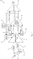
- an optical receiver 1 of the invention has regulated cascode (RGC) circuits 2 and 3 at the inputs to a first amplifier, in this case a differential TIA 4 with an AGC 5.
- RRC regulated cascode
- a differential summing amplifier (DSA) 10 receives the TIA 4 positive and negative outputs TIA_plus and TIA_minus. However, in addition there are two peak detectors 15 and 16. They receive the TIA_plus and TIA_minus signals respectively and provide the amplitude reference PkDet_plus and PkDet_minus outputs to the DSA 10. The defined bandwidth of the DSA is designed to the required application to filter out high frequency noise or disturbances.
- a reset and control circuit 17 is provided for resetting the detectors 15 and 16, and for providing an offset enable V OFFSET_ENABLE signal to a comparator 20 providing the output signal V out .
- the DSA 10 provides DSA_plus and DSA_minus signals as inputs to the comparator 20, and to the AGC (automatic gain control circuit) 5.
- the AGC 5 input requires a linear representation of the received optical light power to assist in the loop design and stability, which is provided by the linear DSA 10 gain.
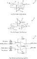
- the peak detector 15 comprises a first amplifier 30 feeding a second amplifier 31 via a diode 33.
- a capacitor C1 to ground providing a peak detected amplitude reference input to the amplifier 30.
- the reset signal is connected to the gate of a switch 32 which links the signal input to the second amplifier 31 to ground.
- the output PkDet_plus is provided by the output of the second amplifier 31.
- the negative peak detector 16 ( Fig. 3(b) ) has a similar architecture, with first and second amplifiers 35 and 36, a capacitor C2, a reset switch 37, and a diode 38.
- the amplifiers 30 and 35 can be identical, as can the amplifiers 31 and 36.
- the DSA 10 ( Fig. 4 ) comprises an amplifier 40 with feedback links via resistors R FB from the DSA_minus and DSA_plus outputs, which ensures that the DSA gain is linear, which is of benefit when using an AGC.
- the peak detector inputs are passed through resistances which are greater than those of the TIA inputs, in this case double. This reduces the gain of the differential peak detector by half compared to the differential TIA signals.
- the amplifier 40 contains common mode feedback with the common mode reference set from the common mode output of the TIA outputs.
- the transducers are a signal receiving photodiode 51 and a dark photodiode 52, both of which are connected to the RGC 2 and 3, which feed into the differential TIA 4 whose gain may be adjusted with the AGC 5 control loop.
- the outputs of the differential TIA 4 feed into the DSA 10 and the two peak detectors 15 and 16 similarly connect into the DSA 10 with half the gain.
- the DSA stage 10 converts a pseudo differential input signal from the differential TIA 4 to a fully differential output signal which is connected to the comparator 20 and the AGC 5.
- the gain of the DSA is linear so that the AGC can automatically control the TIA gain, to ensure there is no saturation of the TIA.
- the comparator 20 may include a hysteresis function.
- the pseudo differential TIA output signals and the peak detected signals from the peak detector are fed into the DSA 10 almost simultaneously, and generate the fully differential output with minimum delay.
- the comparator may also include an offset level control input V OFFSET_ENABLE which ensures the comparator will output a low until the input from the DSA is above an offset level. This can be used to ensure that the comparator outputs a low in static off mode, which is needed for receiving DC or low megahertz data. When light is being received V OFFSET_ENABLE is disabled so that comparator has a zero crossover offset to achieve high quality PWD performance.
- DS A diff DSA _ plus ⁇ DSA _ minus
- TI A diff TI A plus ⁇ TIA _ minus
- Table 1 Outputs for static off, light on and off modes Static off mode Light On Light Off Comment
- Differential TIA output 0 TIA diff 0 Peak Detector Output 0 TIA diff_max where PkDet diff TIA diff_max after 1st pulse of light
- DSA diff TI A diff ⁇ PkDe t diff 2 Offset Level Control V OFFSET_ENABLE Enabled Disabled Enabled only when waiting for 1 st pulse Comparator Output Low High Low
- Fig. 5 illustrates the relevant signals from the block diagram in Figure 2 .
- the signals show the pseudo differential TIA output signals (TIA_plus, TIA_minus).
- the PkDet_plus signal is the maximum of the TIA_plus signal
- the PkDet_minus is the minimum of the TIA_minus signal.
- the TIA output signals, and the positive and negative peak detectors signals are all combined to create the fully differential DSA output signals (DSA_plus, DSA_minus).
- the DSA outputs (DSA_plus, DSA_minus) are used by the comparator to generate the digital comparator output (Comp Vout).
- the comparator has hysteresis controlled by V OFFSET_ENABLE .
- the flow diagram of Fig. 6 describes the operation of the reset (V RESET ) and offset level control (V OFFSET_ENABLE ) signals.
- V RESET reset
- V OFFSET_ENABLE offset level control
- a major benefit of two peak detectors is that they balance the capacitive loading on the differential TIA, which improves the accuracy of the receiver architecture in EMI and noise rejection, and the accuracy for receiving low input power.
- the outputs of the TIA can be unbalanced. This means that the difference between the common mode of the TIA, and its outputs TIA_plus and TIA_minus signals may not be equal. This is illustrated by the deliberately distorted TIA outputs in Fig 7 .
- Combining the two peak detectors and the DSA helps to remove the majority of these unbalanced TIA outputs. With suitable DSA gain, the DSA output is a fully differential output with equal amplitudes for both light on and off cases, even though the TIA outputs are unbalanced. The removal of this distortion results in a low PWD output.
- Fig. 2 has multiple advantageous roles:
- the invention achieves a fully differential output without significant delay because of its ability to produce a fully differential signal on the first pulse, which is important in detecting a signal from a single high speed input pulse.
- the advantages of implementing with two peak detectors and a DSA, with reduced propagation delay ensures that the DSA output will respond with negligible delay to the differential TIA outputs, and with the benefit of a high tolerance to any TIA imbalances.
- the linear gain of the DSA allows the outputs to be used by an AGC, as it a linear representation of the light received.
- differential TIA architecture the balanced load architecture of two peak detectors and the differential summing amplifier will reject any common interference.
- the differential summing amplifier can be used to amplify low amplitude TIA signals, and to filter the signals to the required bandwidth, which improves the signal to noise ratio of the inputs to the comparator.
- the photodiodes are monolithic integrated photodiodes. This is advantageous because there is no wire-bond induced disturbances or noise for the receiver to reject, which would be the case for an external pin photodiode.
Landscapes
- Engineering & Computer Science (AREA)
- Power Engineering (AREA)
- Physics & Mathematics (AREA)
- Electromagnetism (AREA)
- Computer Networks & Wireless Communication (AREA)
- Signal Processing (AREA)
- Amplifiers (AREA)
- Optical Communication System (AREA)
Description
- The invention relates to an optical receiver with a differential output, particularly for control and communication applications.
- In many industrial and/or control applications the receiver in idle mode may be receiving a DC light level and then must respond without fail to the first bit of a command signal data stream sent at any arbitrary time over a wide received optical power range. The conversion of optical light into a voltage is usually implemented using a photodiode and a transimpedance amplifier (TIA). Where the dynamic range of the received light power is wide, a TIA with automatic gain control (AGC) is needed as to reduce the gain for higher received light power. The use of a fully differential TIA is preferred for noise and electromagnetic interference (EMI) immunity.
- A photodiode has a single ended current output. A fully differential TIA outputs a pseudo differential signal, as illustrated by
Fig. 1 , when the input is a single photodiode. Creating an accurate comparator reference point for a pseudo differential signal at high speed instantaneously is difficult. Using a fully differential signal into a comparator ensures that the pulse width distortion (PWD) is low, which is needed for DC to multiple megahertz frequency applications. The circuit shown inFig. 1 is a conventional differential TIA, with the output of such circuit being a pseudo differential signal. - An approach described in [1] below involves use of two low pass filters (LPFs) connected to an output buffer. However, the averaging operations of the LPFs tend to introduce delays.
- An approach in [2] below involves a peak detector feeding back a correction signal to the input of a TIA. This method of feedback control to the input of the TIA is less desirable than a method of feed-forward control, because feedback inherently requires a signal delay.
-
- The following documents describe other optical receivers:
-
US2002/063937 A1 (KIKUCHI OSAMU [JP]) - QUADIR NASIR ABDUL ET AL: "An inductorless linear optical receiver for 20Gbaud/s (40Gb/s) PAM-4 modulation using 28nm CMOS" 2014 IEEE INTERNATIONAL SYMPOSIUM ON CIRCUITS AND SYSTEMS (ISCAS), IEEE, 1 June 2014 (2014-06-01) pages 2473-2476.
-
US6151150 A (KIKUCHI OSAMU [JP]) - The invention is directed towards providing an optical receiver with a fully differential output, without significant delay for receiving DC to multiple megahertz frequency optical light pulses over a large optical received power range, and preferably also with good immunity to both noise and electromagnetic interference (EMI).
References [1] Title: "1.25 Gb/s CMOS Differential Transimpedance Amplifier For Gigabit Networks" Authors: Ty Yoon, Bahram Jalali. Published: Proceedings of the 23rd European Solid-State Circuits Conference, 1997. ESSCIRC '97. Southampton, UK, Pages 140 - 143. [2] Title: "High-speed, Burst-Mode, Packet-Capable Optical Receiver and Instantaneous Clock Recovery for Optical Bus Operation" Authors: Yusuke Ota, Robert G. Swartz, Vance D. Archer 111, Steven K. Korotky, Mihai Banu, and Alfred E. Dunlop. Published: JOURNAL OF LIGHTWAVE TECHNOLOGY, VOL. 12, NO. 2, FEBRUARY 1994, Pages 325- 331. Patent: US 5430766 A , "Burst mode digital data receiver"Filing date Aug 22, 1994 - According to the invention, there is provided an optical receiver as set out in
claim 1. - In one embodiment, one photodiode is active and another photodiode is a dummy photodiode.
- In one embodiment, the differential summing amplifier has linear gain.
- In one embodiment, the differential summing amplifier is an active low pass filter.
- In one embodiment, the peak detector output is fed into the differential summing amplifier with less gain than the differential TIA inputs into the differential summing amplifier.
- In one embodiment, said gain is less by approximately half.
- In one embodiment, the differential summing amplifier is connected at its output to a decision circuit, preferably a comparator.
- In one embodiment, the cascodes are regulated gate cascodes.
- In one embodiment, the receiver further comprises an output comparator linked with the output of the differential summing amplifier, and wherein the output comparator has built-in hysteresis.
- In one embodiment, the receiver further comprises a reset control circuit configured to reset the peak detectors.
- In one embodiment, the output comparator has a DC offset level, with an offset level control input (VOFFSET_ENABLE), which is controlled by the control circuit and is adapted to ensure that the output is low for a minimum light level received.
- In one embodiment, the reset control circuit is configured to assert offset level control (VOFFSET_ENABLE), and reset control (VRESET) after a set timeout period when no light is received.
- In another aspect, the invention provides an electronic or electro-optic device comprising a processing circuit linked to a receiver of any embodiment.
- Also described is a receiver comprising:
- a first amplifier arranged to receive one or more transducer inputs,
- a peak detector arranged to receive an output of the first amplifier,
- a second amplifier arranged to receive the output of the first amplifier and an amplitude reference signal from the peak detector, and
- wherein said second amplifier directly or indirectly provides a receiver output.
- In one embodiment, the first amplifier is a differential amplifier.
- In one embodiment, said first amplifier is a differential transimpedance amplifier (TIA), the transducer providing a current signal.
- In one embodiment, there are two transducer inputs to the first amplifier. In one embodiment, one transducer is active and another transducer is a dummy transducer.
- In one embodiment, the transducer is a photo diode, the receiver, being an optical receiver, and there may also be a dummy or reference photodiode.
- In one embodiment, the first amplifier provides at least two outputs, positive and negative, and there is a peak detector for one or both of said first amplifier outputs.
- In one embodiment, the peak detector is arranged to feed a peak detection signal into the second amplifier simultaneously with an output of the differential TIA, so that the second amplifier provides differential outputs without delay.
- In one embodiment, there is a peak detector receiving each of the positive and negative differential TIA outputs, and each providing a peak detection output to the amplifier.
- In one embodiment, the second amplifier is a differential summing amplifier.
- In one embodiment, the peak detector output is fed to the second amplifier with less gain than the differential TIA output.
- In one embodiment, the gain is reduced by approximately half.
- In one embodiment, the amplifier is connected at its output to a comparator or other decision circuit.
- In one embodiment, the first amplifier has a cascode or a regulated gate cascode at it inputs.
- In one embodiment, the receiver comprises an automatic gain circuit for the second amplifier.
- In one embodiment, there is one peak detector and a common mode buffer amplifier providing signals to the second amplifier.
- In one embodiment, there are positive and negative peak detectors.
- In one embodiment, the receiver comprises at its output a comparator with a DC offset level, which driven by control circuitry ensures the output is low for no light received.
- In one embodiment, the output comparator has built-in hysteresis.
- In one embodiment, the receiver comprises an offset level control input (VOFFSET_ENABLE) which ensures that the comparator will output a low until the input from the second amplifier is above an offset level.
- In one embodiment, a single transducer is used as a detector and the first amplifier is a single ended amplifier, and the second amplifier a differential summing amplifier.
- In another aspect, we describe an electronic or electro-optic device comprising a processing circuit linked to a receiver as defined above in any embodiment.
- The invention will be more clearly understood from the following description of some embodiments thereof, given by way of example only with reference to the accompanying drawings in which:-
-
Fig. 1 is a set of representative plots showing light input signals and pseudo and fully differential outputs, as discussed above with reference to the prior art; -
Fig. 2 is a block diagram of a receiver of the invention; -
Figs. 3(a) and 3(b) are circuit diagrams of positive peak detector and negative peak detector components of the receiver illustrated inFig. 2 ; -
Fig. 4 is a circuit diagram of a differential summing amplifier of the receiver illustrated inFig. 2 ; -
Fig. 5 is a series of plots showing stages of how the receiver provides a fully differential signal; -
Fig. 6 is a logic diagram for operation of the receiver for reset and DC offset level control; and -
Fig. 7 is a series of plots showing stages of how the receiver provides a fully differential signal, from a distorted TIA output. - We describe various optical receivers which have lower distortion. In some embodiments this is achieved because the output crosses the zero line, thereby providing a fully differential output. The receiver has a differential transimpedance amplifier with two inputs and two outputs. The differential transimpedance amplifier, provides a differential output and this is peak-detected to provide amplitude reference signals. The differential transimpedance amplifier output and the amplitude reference signals are fed to a differential summing amplifier, which provides a fully differential output to a comparator, or an automatic gain control circuit to regulate the differential transimpedance amplifier gain.
- Referring to
Fig. 2 anoptical receiver 1 of the invention has regulated cascode (RGC)circuits differential TIA 4 with anAGC 5. - A differential summing amplifier (DSA) 10 receives the
TIA 4 positive and negative outputs TIA_plus and TIA_minus. However, in addition there are twopeak detectors DSA 10. The defined bandwidth of the DSA is designed to the required application to filter out high frequency noise or disturbances. A reset andcontrol circuit 17 is provided for resetting thedetectors comparator 20 providing the output signal Vout. - The
DSA 10 provides DSA_plus and DSA_minus signals as inputs to thecomparator 20, and to the AGC (automatic gain control circuit) 5. TheAGC 5 input requires a linear representation of the received optical light power to assist in the loop design and stability, which is provided by thelinear DSA 10 gain. - As shown in
Fig. 3(a) thepeak detector 15 comprises afirst amplifier 30 feeding asecond amplifier 31 via adiode 33. There is a capacitor C1 to ground providing a peak detected amplitude reference input to theamplifier 30. The reset signal is connected to the gate of aswitch 32 which links the signal input to thesecond amplifier 31 to ground. The output PkDet_plus is provided by the output of thesecond amplifier 31. - The negative peak detector 16 (
Fig. 3(b) ) has a similar architecture, with first andsecond amplifiers reset switch 37, and adiode 38. In most applications theamplifiers amplifiers - The DSA 10 (
Fig. 4 ) comprises anamplifier 40 with feedback links via resistors RFB from the DSA_minus and DSA_plus outputs, which ensures that the DSA gain is linear, which is of benefit when using an AGC. The peak detector inputs are passed through resistances which are greater than those of the TIA inputs, in this case double. This reduces the gain of the differential peak detector by half compared to the differential TIA signals. Theamplifier 40 contains common mode feedback with the common mode reference set from the common mode output of the TIA outputs. - In more detail, and referring again also to
Fig. 2 , the transducers are asignal receiving photodiode 51 and adark photodiode 52, both of which are connected to theRGC differential TIA 4 whose gain may be adjusted with theAGC 5 control loop. The outputs of thedifferential TIA 4 feed into theDSA 10 and the twopeak detectors DSA 10 with half the gain. TheDSA stage 10 converts a pseudo differential input signal from thedifferential TIA 4 to a fully differential output signal which is connected to thecomparator 20 and theAGC 5. The gain of the DSA is linear so that the AGC can automatically control the TIA gain, to ensure there is no saturation of the TIA. Thecomparator 20 may include a hysteresis function. The pseudo differential TIA output signals and the peak detected signals from the peak detector are fed into theDSA 10 almost simultaneously, and generate the fully differential output with minimum delay. The comparator may also include an offset level control input VOFFSET_ENABLE which ensures the comparator will output a low until the input from the DSA is above an offset level. This can be used to ensure that the comparator outputs a low in static off mode, which is needed for receiving DC or low megahertz data. When light is being received VOFFSET_ENABLE is disabled so that comparator has a zero crossover offset to achieve high quality PWD performance. -
Fig. 4 shows the DSA circuit with the output equal to:


- The


- Table 1 below describes the output states of the TIA, Peak Detector, DSA, DC Ref Level input, and comparator output, for static off, light on and off modes, assuming GainDSA = 1.
Table 1. Outputs for static off, light on and off modes Static off mode Light On Light Off Comment Differential TIA output 0 TIAdiff 0 Peak Detector Output 0 TIAdiff_max where PkDetdiff = TIAdiff_max after 1st pulse of light Differential Summing Amplifier (DSA) output 0 

where DSAdiff = 
Offset Level Control VOFFSET_ENABLE Enabled Disabled Enabled only when waiting for 1st pulse Comparator Output Low High Low -
Fig. 5 illustrates the relevant signals from the block diagram inFigure 2 . The signals show the pseudo differential TIA output signals (TIA_plus, TIA_minus). The PkDet_plus signal is the maximum of the TIA_plus signal, and the PkDet_minus is the minimum of the TIA_minus signal. The TIA output signals, and the positive and negative peak detectors signals are all combined to create the fully differential DSA output signals (DSA_plus, DSA_minus). The DSA outputs (DSA_plus, DSA_minus) are used by the comparator to generate the digital comparator output (Comp Vout). The comparator has hysteresis controlled by VOFFSET_ENABLE. - The flow diagram of
Fig. 6 describes the operation of the reset (VRESET) and offset level control (VOFFSET_ENABLE) signals. Once in static off mode, if light is received then the VOFFSET_ENABLE is disabled into the comparator. If no light is received for a timeout period then the VOFFSET_ENABLE is enabled and the peak detectors are reset so the receiver returns to static off mode. This control of the VOFFSET_ENABLE signal allows the receiver to receive DC to megahertz data. - A major benefit of two peak detectors is that they balance the capacitive loading on the differential TIA, which improves the accuracy of the receiver architecture in EMI and noise rejection, and the accuracy for receiving low input power. When light is received the outputs of the TIA can be unbalanced. This means that the difference between the common mode of the TIA, and its outputs TIA_plus and TIA_minus signals may not be equal. This is illustrated by the deliberately distorted TIA outputs in
Fig 7 . Combining the two peak detectors and the DSA helps to remove the majority of these unbalanced TIA outputs. With suitable DSA gain, the DSA output is a fully differential output with equal amplitudes for both light on and off cases, even though the TIA outputs are unbalanced. The removal of this distortion results in a low PWD output. - The architecture in
Fig. 2 has multiple advantageous roles: - (a) Creation of a fully differential signal from the pseudo differential TIA outputs.
- (b) Provides equal loading on the TIA outputs, which keeps the architecture symmetric.
- (c) Reduces most of the possible imbalance in the TIA outputs for received light.
- (d) The DSA amplifies the signal from the TIA outputs for low received light power.
- (e) The DSA filters the signals to the required bandwidth so that no high frequency noise is fed through to the
comparator 20. - (f) The DSA provides a linear representation of the light received to the AGC, with the linear DSA gain.
- (g) Insofar as possible a symmetric differential architecture is created from the TIA outputs to the comparator inputs.
- It will be appreciated that the invention achieves a fully differential output without significant delay because of its ability to produce a fully differential signal on the first pulse, which is important in detecting a signal from a single high speed input pulse. The advantages of implementing with two peak detectors and a DSA, with reduced propagation delay ensures that the DSA output will respond with negligible delay to the differential TIA outputs, and with the benefit of a high tolerance to any TIA imbalances. The linear gain of the DSA allows the outputs to be used by an AGC, as it a linear representation of the light received.
- Also, there is reduced noise induced by EMI and other sources because the differential TIA architecture, the balanced load architecture of two peak detectors and the differential summing amplifier will reject any common interference. The differential summing amplifier can be used to amplify low amplitude TIA signals, and to filter the signals to the required bandwidth, which improves the signal to noise ratio of the inputs to the comparator.
- The invention is not limited to the embodiments described but may be varied in construction and detail. In one example the photodiodes are monolithic integrated photodiodes. This is advantageous because there is no wire-bond induced disturbances or noise for the receiver to reject, which would be the case for an external pin photodiode.
Claims (13)
- An optical receiver comprising:a differential transimpedance amplifier TIA (4) having input cascodes (2, 3), and being arranged to receive one or more photodiode (51, 52) inputs and to provide at least two outputs, positive and negative,a positive peak detector (15) receiving the positive differential TIA (4) output, a negative peak detector (16) receiving the negative differential TIA (4) output, and each providing a peak detection output as an amplitude reference signal,a differential summing amplifier (10) arranged to receive the outputs of the differential TIA (4) and the amplitude reference signals from the peak detectors (15, 16),wherein said differential summing amplifier (10) directly or indirectly provides an output for the optical receiver,wherein the receiver further comprises an automatic gain circuit (5) for the differential transimpedance amplifier (4), and wherein the differential summing amplifier (10) is connected at its output to the automatic gain circuit (5).
- An optical receiver as claimed in claim 1, wherein one photodiode (51) is active and another photodiode (52) is a dummy photodiode.
- An optical receiver as claimed in claims 1 or 2, wherein the differential summing amplifier (10) has linear gain.
- An optical receiver as claimed in any preceding claim, wherein the differential summing amplifier (10) is an active low pass filter.
- An optical receiver as claimed in any preceding claim, wherein the peak detector output is fed into the differential summing amplifier (10) with less gain than gain of the differential TIA (4) inputs into the differential summing amplifier (10).
- An optical receiver as claimed in claim 5, wherein said gain of the peak detector output is less by approximately half.
- An optical receiver as claimed in any preceding claim, wherein the differential summing amplifier (10) is connected at its output to a decision circuit, preferably a comparator (20).
- An optical receiver as claimed in any preceding claim, wherein the cascodes are regulated gate cascodes (2, 3).
- An optical receiver as claimed in any preceding claim, further comprising an output comparator (20) linked with the output of the differential summing amplifier, and wherein the output comparator (20) has built-in hysteresis.
- An optical receiver as claimed in any preceding claim further comprising a reset control circuit (17) configured to reset the peak detectors (15, 16).
- An optical receiver as claimed in either of claims 9 or 10, wherein the output comparator (20) has a DC offset level, with an offset level control input (VOFFSET_ENABLE), which is controlled by the control circuit (17) and is adapted to ensure that the output is low for a minimum light level received.
- An optical receiver as claimed in either of claims 10 or 11, where the reset control circuit (17) is configured to assert offset level control (VOFFSET_ENABLE), and reset control (VRESET) after a set timeout period when no light is received.
- An electronic or electro-optic device comprising a processing circuit linked to a receiver of any preceding claim.
Applications Claiming Priority (2)
| Application Number | Priority Date | Filing Date | Title |
|---|---|---|---|
| EP15185216 | 2015-09-15 | ||
| PCT/EP2016/071526 WO2017046067A1 (en) | 2015-09-15 | 2016-09-13 | An optical receiver |
Publications (2)
| Publication Number | Publication Date |
|---|---|
| EP3350919A1 EP3350919A1 (en) | 2018-07-25 |
| EP3350919B1 true EP3350919B1 (en) | 2019-07-31 |
Family
ID=54145671
Family Applications (1)
| Application Number | Title | Priority Date | Filing Date |
|---|---|---|---|
| EP16763847.7A Active EP3350919B1 (en) | 2015-09-15 | 2016-09-13 | An optical receiver |
Country Status (4)
| Country | Link |
|---|---|
| US (1) | US10333472B2 (en) |
| EP (1) | EP3350919B1 (en) |
| CN (1) | CN108141186A (en) |
| WO (1) | WO2017046067A1 (en) |
Families Citing this family (7)
| Publication number | Priority date | Publication date | Assignee | Title |
|---|---|---|---|---|
| CN108141286A (en) * | 2015-09-15 | 2018-06-08 | 法尔科姆斯有限公司 | Optical receiver with cascade front end |
| WO2017074385A1 (en) * | 2015-10-29 | 2017-05-04 | Hewlett-Packard Enterprise | Receivers with automatic gain control |
| CN110999074B (en) * | 2017-08-12 | 2023-04-11 | 卢克斯特拉有限公司 | Method and system for waveguide delay based equalization using optical splitting in optical communications |
| CN109861761B (en) * | 2019-03-01 | 2021-04-23 | 电子科技大学 | A CMOS High-speed Optical Receiver Circuit Based on Peak Sampling |
| CN113644884A (en) * | 2021-07-27 | 2021-11-12 | 宁波群芯微电子有限责任公司 | Transimpedance amplifying circuit and photosensitive chip |
| CN116436530A (en) * | 2022-01-13 | 2023-07-14 | 意法半导体(格勒诺布尔2)公司 | Receiver device, receiving system, processing and optical signal communication method |
| TWI842185B (en) * | 2022-11-08 | 2024-05-11 | 台亞半導體股份有限公司 | Light receiving circuit |
Family Cites Families (25)
| Publication number | Priority date | Publication date | Assignee | Title |
|---|---|---|---|---|
| US4498001A (en) | 1982-07-26 | 1985-02-05 | At&T Bell Laboratories | Transimpedance amplifier for optical receivers |
| JP2503837B2 (en) | 1992-07-16 | 1996-06-05 | 日本電気株式会社 | Digital optical receiver circuit and preamplifier circuit in digital optical receiver circuit |
| CA2106439A1 (en) | 1992-11-13 | 1994-05-14 | Yusuke Ota | Burst mode digital data receiver |
| JP2656734B2 (en) * | 1994-09-12 | 1997-09-24 | 宮城日本電気株式会社 | Optical receiving circuit |
| JP3357772B2 (en) | 1995-03-31 | 2002-12-16 | 株式会社東芝 | Receiver circuit, optical receiver circuit, optical receiver module, and optical wiring module set |
| JPH1084231A (en) * | 1996-05-24 | 1998-03-31 | Toshiba Corp | Digital signal receiving circuit |
| JP3340341B2 (en) * | 1996-10-03 | 2002-11-05 | 沖電気工業株式会社 | Level identification circuit |
| US5793230A (en) * | 1997-02-26 | 1998-08-11 | Sandia Corporation | Sensor readout detector circuit |
| FI974225A7 (en) * | 1997-11-13 | 1999-05-14 | Nokia Corp | Optical receiver |
| JP3085275B2 (en) * | 1998-02-18 | 2000-09-04 | 日本電気株式会社 | Binary optical transmission method and binary optical transmission system |
| EP0981197A4 (en) * | 1998-03-13 | 2005-03-30 | Matsushita Electric Industrial Co Ltd | AMPLIFIER CIRCUIT, AND OPTICAL RECEIVER EQUIPPED WITH THIS CIRCUIT |
| US6084478A (en) * | 1998-08-20 | 2000-07-04 | Vitesse Semiconductor Corp. | Transimpedance amplifier with automatic gain control |
| JP2002164855A (en) * | 2000-11-29 | 2002-06-07 | Oki Electric Ind Co Ltd | Optical reception circuit |
| US6963696B1 (en) * | 2001-04-30 | 2005-11-08 | Quantum Bridge Communications, Inc. | AC-coupled burst mode receiver with wide dynamic range |
| JP5339088B2 (en) * | 2007-11-30 | 2013-11-13 | 日本電気株式会社 | Optical receiving circuit and signal processing method |
| CN101197623B (en) * | 2007-12-18 | 2012-06-13 | 天津大学 | Difference light receiver and method for simultaneously multiplying sensibility and band width |
| US8189419B2 (en) * | 2009-07-06 | 2012-05-29 | International Business Machines Corporation | Apparatus for nonvolatile multi-programmable electronic fuse system |
| CN101621283A (en) * | 2009-08-07 | 2010-01-06 | 天津泛海科技有限公司 | Amplitude detection and automatic gain control (AGC) circuit |
| JP5459103B2 (en) * | 2010-06-25 | 2014-04-02 | 住友電気工業株式会社 | Amplifier circuit |
| JP5596860B2 (en) * | 2011-06-30 | 2014-09-24 | 日本電信電話株式会社 | Automatic gain adjustment circuit |
| CN102412906A (en) * | 2011-08-08 | 2012-04-11 | 中兴通讯股份有限公司 | Differential Quadrature Phase Shift Keying Receiver and Its Gain Control Method |
| JP5944750B2 (en) * | 2012-06-06 | 2016-07-05 | 日本電信電話株式会社 | Optical signal detection circuit |
| US9509413B2 (en) * | 2012-11-01 | 2016-11-29 | Nec Corporation | Optical receiver, optical receiving device, and method for correcting received optical intensity |
| JP6413265B2 (en) * | 2014-03-12 | 2018-10-31 | 住友電気工業株式会社 | Optical modulator drive circuit |
| US10128398B1 (en) * | 2014-05-23 | 2018-11-13 | Stc.Unm | Resonance avalanche photodiodes for dynamic biasing |
-
2016
- 2016-09-13 EP EP16763847.7A patent/EP3350919B1/en active Active
- 2016-09-13 WO PCT/EP2016/071526 patent/WO2017046067A1/en not_active Ceased
- 2016-09-13 CN CN201680061518.3A patent/CN108141186A/en active Pending
- 2016-09-13 US US15/758,414 patent/US10333472B2/en active Active
Non-Patent Citations (1)
| Title |
|---|
| None * |
Also Published As
| Publication number | Publication date |
|---|---|
| US20180254756A1 (en) | 2018-09-06 |
| WO2017046067A1 (en) | 2017-03-23 |
| CN108141186A (en) | 2018-06-08 |
| EP3350919A1 (en) | 2018-07-25 |
| US10333472B2 (en) | 2019-06-25 |
Similar Documents
| Publication | Publication Date | Title |
|---|---|---|
| US10333472B2 (en) | Optical receiver | |
| KR101911134B1 (en) | Receiver having a wide common mode input range | |
| JP3502264B2 (en) | Receiver | |
| CN1977473B (en) | Transimpedance amplifier with integrated filtering and reduced parasitic capacitance | |
| JP3576702B2 (en) | Variable high-pass filter | |
| US7123098B2 (en) | Transimpedance amplifier with differential peak detector | |
| JP2000201114A (en) | High speed differential type photoelectric receiver | |
| WO2009055035A2 (en) | High sensitivity two-stage amplifier | |
| US7406268B2 (en) | Optical receiver circuit | |
| US7030702B2 (en) | Optical receiver with wide dynamic range transimpedance amplifier | |
| EP3350945B1 (en) | An optical receiver with a cascode front end | |
| JP6661057B1 (en) | Limiting amplifier circuit | |
| JP2002164855A (en) | Optical reception circuit | |
| JP2011109721A (en) | Amplitude limit amplifier circuit | |
| EP2418789B1 (en) | Optoelectronic device for differential photoreception, with automatic compensation of phase and amplitude imbalances | |
| JP3606143B2 (en) | Offset control circuit, optical receiver using the same, and optical communication system | |
| CN102723944B (en) | A kind of method and circuit single-ended signal being converted to differential signal | |
| JP2009239330A (en) | Amplitude limit amplifier circuit | |
| US6552615B1 (en) | Method and system for compensation of low-frequency photodiode current in a transimpedance amplifier | |
| CA2263053A1 (en) | Differential optical signal receiver | |
| US20050051703A1 (en) | Power supply rejection for high bandwidth transimpedance amplifier circuits (TIAs) | |
| US9843297B2 (en) | Balanced differential transimpedance amplifier with single ended input and balancing method | |
| JP6534187B2 (en) | Transimpedance amplifier circuit | |
| KR102923920B1 (en) | Trans-impedance amplifier and photoelectric conversion circuit | |
| KR101128451B1 (en) | Input signal amplifying device |
Legal Events
| Date | Code | Title | Description |
|---|---|---|---|
| STAA | Information on the status of an ep patent application or granted ep patent |
Free format text: STATUS: THE INTERNATIONAL PUBLICATION HAS BEEN MADE |
|
| PUAI | Public reference made under article 153(3) epc to a published international application that has entered the european phase |
Free format text: ORIGINAL CODE: 0009012 |
|
| STAA | Information on the status of an ep patent application or granted ep patent |
Free format text: STATUS: REQUEST FOR EXAMINATION WAS MADE |
|
| 17P | Request for examination filed |
Effective date: 20180410 |
|
| AK | Designated contracting states |
Kind code of ref document: A1 Designated state(s): AL AT BE BG CH CY CZ DE DK EE ES FI FR GB GR HR HU IE IS IT LI LT LU LV MC MK MT NL NO PL PT RO RS SE SI SK SM TR |
|
| AX | Request for extension of the european patent |
Extension state: BA ME |
|
| DAV | Request for validation of the european patent (deleted) | ||
| DAX | Request for extension of the european patent (deleted) | ||
| GRAP | Despatch of communication of intention to grant a patent |
Free format text: ORIGINAL CODE: EPIDOSNIGR1 |
|
| STAA | Information on the status of an ep patent application or granted ep patent |
Free format text: STATUS: GRANT OF PATENT IS INTENDED |
|
| RIC1 | Information provided on ipc code assigned before grant |
Ipc: H04B 10/69 20130101ALI20190326BHEP Ipc: H03G 3/30 20060101ALI20190326BHEP Ipc: H03H 11/12 20060101ALI20190326BHEP Ipc: H03F 3/45 20060101ALI20190326BHEP Ipc: H03F 3/08 20060101AFI20190326BHEP |
|
| INTG | Intention to grant announced |
Effective date: 20190412 |
|
| GRAS | Grant fee paid |
Free format text: ORIGINAL CODE: EPIDOSNIGR3 |
|
| GRAA | (expected) grant |
Free format text: ORIGINAL CODE: 0009210 |
|
| STAA | Information on the status of an ep patent application or granted ep patent |
Free format text: STATUS: THE PATENT HAS BEEN GRANTED |
|
| AK | Designated contracting states |
Kind code of ref document: B1 Designated state(s): AL AT BE BG CH CY CZ DE DK EE ES FI FR GB GR HR HU IE IS IT LI LT LU LV MC MK MT NL NO PL PT RO RS SE SI SK SM TR |
|
| REG | Reference to a national code |
Ref country code: CH Ref legal event code: EP Ref country code: GB Ref legal event code: FG4D |
|
| REG | Reference to a national code |
Ref country code: AT Ref legal event code: REF Ref document number: 1162015 Country of ref document: AT Kind code of ref document: T Effective date: 20190815 |
|
| REG | Reference to a national code |
Ref country code: IE Ref legal event code: FG4D |
|
| REG | Reference to a national code |
Ref country code: DE Ref legal event code: R096 Ref document number: 602016017790 Country of ref document: DE |
|
| REG | Reference to a national code |
Ref country code: NL Ref legal event code: MP Effective date: 20190731 |
|
| REG | Reference to a national code |
Ref country code: LT Ref legal event code: MG4D |
|
| REG | Reference to a national code |
Ref country code: AT Ref legal event code: MK05 Ref document number: 1162015 Country of ref document: AT Kind code of ref document: T Effective date: 20190731 |
|
| PG25 | Lapsed in a contracting state [announced via postgrant information from national office to epo] |
Ref country code: NO Free format text: LAPSE BECAUSE OF FAILURE TO SUBMIT A TRANSLATION OF THE DESCRIPTION OR TO PAY THE FEE WITHIN THE PRESCRIBED TIME-LIMIT Effective date: 20191031 Ref country code: NL Free format text: LAPSE BECAUSE OF FAILURE TO SUBMIT A TRANSLATION OF THE DESCRIPTION OR TO PAY THE FEE WITHIN THE PRESCRIBED TIME-LIMIT Effective date: 20190731 Ref country code: AT Free format text: LAPSE BECAUSE OF FAILURE TO SUBMIT A TRANSLATION OF THE DESCRIPTION OR TO PAY THE FEE WITHIN THE PRESCRIBED TIME-LIMIT Effective date: 20190731 Ref country code: PT Free format text: LAPSE BECAUSE OF FAILURE TO SUBMIT A TRANSLATION OF THE DESCRIPTION OR TO PAY THE FEE WITHIN THE PRESCRIBED TIME-LIMIT Effective date: 20191202 Ref country code: LT Free format text: LAPSE BECAUSE OF FAILURE TO SUBMIT A TRANSLATION OF THE DESCRIPTION OR TO PAY THE FEE WITHIN THE PRESCRIBED TIME-LIMIT Effective date: 20190731 Ref country code: BG Free format text: LAPSE BECAUSE OF FAILURE TO SUBMIT A TRANSLATION OF THE DESCRIPTION OR TO PAY THE FEE WITHIN THE PRESCRIBED TIME-LIMIT Effective date: 20191031 Ref country code: FI Free format text: LAPSE BECAUSE OF FAILURE TO SUBMIT A TRANSLATION OF THE DESCRIPTION OR TO PAY THE FEE WITHIN THE PRESCRIBED TIME-LIMIT Effective date: 20190731 Ref country code: HR Free format text: LAPSE BECAUSE OF FAILURE TO SUBMIT A TRANSLATION OF THE DESCRIPTION OR TO PAY THE FEE WITHIN THE PRESCRIBED TIME-LIMIT Effective date: 20190731 Ref country code: SE Free format text: LAPSE BECAUSE OF FAILURE TO SUBMIT A TRANSLATION OF THE DESCRIPTION OR TO PAY THE FEE WITHIN THE PRESCRIBED TIME-LIMIT Effective date: 20190731 |
|
| PG25 | Lapsed in a contracting state [announced via postgrant information from national office to epo] |
Ref country code: AL Free format text: LAPSE BECAUSE OF FAILURE TO SUBMIT A TRANSLATION OF THE DESCRIPTION OR TO PAY THE FEE WITHIN THE PRESCRIBED TIME-LIMIT Effective date: 20190731 Ref country code: ES Free format text: LAPSE BECAUSE OF FAILURE TO SUBMIT A TRANSLATION OF THE DESCRIPTION OR TO PAY THE FEE WITHIN THE PRESCRIBED TIME-LIMIT Effective date: 20190731 Ref country code: RS Free format text: LAPSE BECAUSE OF FAILURE TO SUBMIT A TRANSLATION OF THE DESCRIPTION OR TO PAY THE FEE WITHIN THE PRESCRIBED TIME-LIMIT Effective date: 20190731 Ref country code: IS Free format text: LAPSE BECAUSE OF FAILURE TO SUBMIT A TRANSLATION OF THE DESCRIPTION OR TO PAY THE FEE WITHIN THE PRESCRIBED TIME-LIMIT Effective date: 20191130 Ref country code: LV Free format text: LAPSE BECAUSE OF FAILURE TO SUBMIT A TRANSLATION OF THE DESCRIPTION OR TO PAY THE FEE WITHIN THE PRESCRIBED TIME-LIMIT Effective date: 20190731 Ref country code: GR Free format text: LAPSE BECAUSE OF FAILURE TO SUBMIT A TRANSLATION OF THE DESCRIPTION OR TO PAY THE FEE WITHIN THE PRESCRIBED TIME-LIMIT Effective date: 20191101 |
|
| PG25 | Lapsed in a contracting state [announced via postgrant information from national office to epo] |
Ref country code: TR Free format text: LAPSE BECAUSE OF FAILURE TO SUBMIT A TRANSLATION OF THE DESCRIPTION OR TO PAY THE FEE WITHIN THE PRESCRIBED TIME-LIMIT Effective date: 20190731 |
|
| PG25 | Lapsed in a contracting state [announced via postgrant information from national office to epo] |
Ref country code: IT Free format text: LAPSE BECAUSE OF FAILURE TO SUBMIT A TRANSLATION OF THE DESCRIPTION OR TO PAY THE FEE WITHIN THE PRESCRIBED TIME-LIMIT Effective date: 20190731 Ref country code: DK Free format text: LAPSE BECAUSE OF FAILURE TO SUBMIT A TRANSLATION OF THE DESCRIPTION OR TO PAY THE FEE WITHIN THE PRESCRIBED TIME-LIMIT Effective date: 20190731 Ref country code: EE Free format text: LAPSE BECAUSE OF FAILURE TO SUBMIT A TRANSLATION OF THE DESCRIPTION OR TO PAY THE FEE WITHIN THE PRESCRIBED TIME-LIMIT Effective date: 20190731 Ref country code: PL Free format text: LAPSE BECAUSE OF FAILURE TO SUBMIT A TRANSLATION OF THE DESCRIPTION OR TO PAY THE FEE WITHIN THE PRESCRIBED TIME-LIMIT Effective date: 20190731 Ref country code: RO Free format text: LAPSE BECAUSE OF FAILURE TO SUBMIT A TRANSLATION OF THE DESCRIPTION OR TO PAY THE FEE WITHIN THE PRESCRIBED TIME-LIMIT Effective date: 20190731 |
|
| PG25 | Lapsed in a contracting state [announced via postgrant information from national office to epo] |
Ref country code: MC Free format text: LAPSE BECAUSE OF FAILURE TO SUBMIT A TRANSLATION OF THE DESCRIPTION OR TO PAY THE FEE WITHIN THE PRESCRIBED TIME-LIMIT Effective date: 20190731 Ref country code: IS Free format text: LAPSE BECAUSE OF FAILURE TO SUBMIT A TRANSLATION OF THE DESCRIPTION OR TO PAY THE FEE WITHIN THE PRESCRIBED TIME-LIMIT Effective date: 20200224 Ref country code: SK Free format text: LAPSE BECAUSE OF FAILURE TO SUBMIT A TRANSLATION OF THE DESCRIPTION OR TO PAY THE FEE WITHIN THE PRESCRIBED TIME-LIMIT Effective date: 20190731 Ref country code: CZ Free format text: LAPSE BECAUSE OF FAILURE TO SUBMIT A TRANSLATION OF THE DESCRIPTION OR TO PAY THE FEE WITHIN THE PRESCRIBED TIME-LIMIT Effective date: 20190731 Ref country code: SM Free format text: LAPSE BECAUSE OF FAILURE TO SUBMIT A TRANSLATION OF THE DESCRIPTION OR TO PAY THE FEE WITHIN THE PRESCRIBED TIME-LIMIT Effective date: 20190731 |
|
| REG | Reference to a national code |
Ref country code: CH Ref legal event code: PL |
|
| REG | Reference to a national code |
Ref country code: DE Ref legal event code: R097 Ref document number: 602016017790 Country of ref document: DE |
|
| PLBE | No opposition filed within time limit |
Free format text: ORIGINAL CODE: 0009261 |
|
| STAA | Information on the status of an ep patent application or granted ep patent |
Free format text: STATUS: NO OPPOSITION FILED WITHIN TIME LIMIT |
|
| PG2D | Information on lapse in contracting state deleted |
Ref country code: IS |
|
| PG25 | Lapsed in a contracting state [announced via postgrant information from national office to epo] |
Ref country code: LI Free format text: LAPSE BECAUSE OF NON-PAYMENT OF DUE FEES Effective date: 20190930 Ref country code: IE Free format text: LAPSE BECAUSE OF NON-PAYMENT OF DUE FEES Effective date: 20190913 Ref country code: LU Free format text: LAPSE BECAUSE OF NON-PAYMENT OF DUE FEES Effective date: 20190913 Ref country code: CH Free format text: LAPSE BECAUSE OF NON-PAYMENT OF DUE FEES Effective date: 20190930 Ref country code: IS Free format text: LAPSE BECAUSE OF FAILURE TO SUBMIT A TRANSLATION OF THE DESCRIPTION OR TO PAY THE FEE WITHIN THE PRESCRIBED TIME-LIMIT Effective date: 20191030 |
|
| REG | Reference to a national code |
Ref country code: BE Ref legal event code: MM Effective date: 20190930 |
|
| 26N | No opposition filed |
Effective date: 20200603 |
|
| PG25 | Lapsed in a contracting state [announced via postgrant information from national office to epo] |
Ref country code: SI Free format text: LAPSE BECAUSE OF FAILURE TO SUBMIT A TRANSLATION OF THE DESCRIPTION OR TO PAY THE FEE WITHIN THE PRESCRIBED TIME-LIMIT Effective date: 20190731 Ref country code: BE Free format text: LAPSE BECAUSE OF NON-PAYMENT OF DUE FEES Effective date: 20190930 |
|
| PG25 | Lapsed in a contracting state [announced via postgrant information from national office to epo] |
Ref country code: FR Free format text: LAPSE BECAUSE OF NON-PAYMENT OF DUE FEES Effective date: 20190930 |
|
| GBPC | Gb: european patent ceased through non-payment of renewal fee |
Effective date: 20200913 |
|
| PG25 | Lapsed in a contracting state [announced via postgrant information from national office to epo] |
Ref country code: CY Free format text: LAPSE BECAUSE OF FAILURE TO SUBMIT A TRANSLATION OF THE DESCRIPTION OR TO PAY THE FEE WITHIN THE PRESCRIBED TIME-LIMIT Effective date: 20190731 |
|
| PG25 | Lapsed in a contracting state [announced via postgrant information from national office to epo] |
Ref country code: HU Free format text: LAPSE BECAUSE OF FAILURE TO SUBMIT A TRANSLATION OF THE DESCRIPTION OR TO PAY THE FEE WITHIN THE PRESCRIBED TIME-LIMIT; INVALID AB INITIO Effective date: 20160913 Ref country code: MT Free format text: LAPSE BECAUSE OF FAILURE TO SUBMIT A TRANSLATION OF THE DESCRIPTION OR TO PAY THE FEE WITHIN THE PRESCRIBED TIME-LIMIT Effective date: 20190731 |
|
| PG25 | Lapsed in a contracting state [announced via postgrant information from national office to epo] |
Ref country code: GB Free format text: LAPSE BECAUSE OF NON-PAYMENT OF DUE FEES Effective date: 20200913 |
|
| PG25 | Lapsed in a contracting state [announced via postgrant information from national office to epo] |
Ref country code: MK Free format text: LAPSE BECAUSE OF FAILURE TO SUBMIT A TRANSLATION OF THE DESCRIPTION OR TO PAY THE FEE WITHIN THE PRESCRIBED TIME-LIMIT Effective date: 20190731 |
|
| P01 | Opt-out of the competence of the unified patent court (upc) registered |
Effective date: 20230413 |
|
| PGFP | Annual fee paid to national office [announced via postgrant information from national office to epo] |
Ref country code: DE Payment date: 20250811 Year of fee payment: 10 |