EP3350945B1 - An optical receiver with a cascode front end - Google Patents
An optical receiver with a cascode front end Download PDFInfo
- Publication number
- EP3350945B1 EP3350945B1 EP16763848.5A EP16763848A EP3350945B1 EP 3350945 B1 EP3350945 B1 EP 3350945B1 EP 16763848 A EP16763848 A EP 16763848A EP 3350945 B1 EP3350945 B1 EP 3350945B1
- Authority
- EP
- European Patent Office
- Prior art keywords
- tia
- circuit
- optical receiver
- signal
- input
- Prior art date
- Legal status (The legal status is an assumption and is not a legal conclusion. Google has not performed a legal analysis and makes no representation as to the accuracy of the status listed.)
- Active
Links
- 230000003287 optical effect Effects 0.000 title claims description 37
- 230000001105 regulatory effect Effects 0.000 claims description 7
- 230000003362 replicative effect Effects 0.000 claims description 3
- 230000008901 benefit Effects 0.000 description 7
- 238000010586 diagram Methods 0.000 description 4
- 238000004513 sizing Methods 0.000 description 2
- 235000004348 Perilla frutescens Nutrition 0.000 description 1
- 244000124853 Perilla frutescens Species 0.000 description 1
- 241001620634 Roger Species 0.000 description 1
- 229910000577 Silicon-germanium Inorganic materials 0.000 description 1
- 230000009286 beneficial effect Effects 0.000 description 1
- 238000006243 chemical reaction Methods 0.000 description 1
- 238000010276 construction Methods 0.000 description 1
- 238000005516 engineering process Methods 0.000 description 1
- 230000036039 immunity Effects 0.000 description 1
- 238000000034 method Methods 0.000 description 1
- 238000011084 recovery Methods 0.000 description 1
- 230000003068 static effect Effects 0.000 description 1
Images


Classifications
-
- H—ELECTRICITY
- H04—ELECTRIC COMMUNICATION TECHNIQUE
- H04B—TRANSMISSION
- H04B10/00—Transmission systems employing electromagnetic waves other than radio-waves, e.g. infrared, visible or ultraviolet light, or employing corpuscular radiation, e.g. quantum communication
- H04B10/60—Receivers
- H04B10/66—Non-coherent receivers, e.g. using direct detection
- H04B10/69—Electrical arrangements in the receiver
- H04B10/693—Arrangements for optimizing the preamplifier in the receiver
- H04B10/6931—Automatic gain control of the preamplifier
-
- H—ELECTRICITY
- H04—ELECTRIC COMMUNICATION TECHNIQUE
- H04B—TRANSMISSION
- H04B10/00—Transmission systems employing electromagnetic waves other than radio-waves, e.g. infrared, visible or ultraviolet light, or employing corpuscular radiation, e.g. quantum communication
- H04B10/60—Receivers
- H04B10/61—Coherent receivers
- H04B10/616—Details of the electronic signal processing in coherent optical receivers
-
- H—ELECTRICITY
- H04—ELECTRIC COMMUNICATION TECHNIQUE
- H04B—TRANSMISSION
- H04B10/00—Transmission systems employing electromagnetic waves other than radio-waves, e.g. infrared, visible or ultraviolet light, or employing corpuscular radiation, e.g. quantum communication
- H04B10/60—Receivers
- H04B10/66—Non-coherent receivers, e.g. using direct detection
- H04B10/69—Electrical arrangements in the receiver
- H04B10/691—Arrangements for optimizing the photodetector in the receiver
-
- H—ELECTRICITY
- H04—ELECTRIC COMMUNICATION TECHNIQUE
- H04B—TRANSMISSION
- H04B10/00—Transmission systems employing electromagnetic waves other than radio-waves, e.g. infrared, visible or ultraviolet light, or employing corpuscular radiation, e.g. quantum communication
- H04B10/60—Receivers
- H04B10/66—Non-coherent receivers, e.g. using direct detection
- H04B10/69—Electrical arrangements in the receiver
- H04B10/693—Arrangements for optimizing the preamplifier in the receiver
- H04B10/6933—Offset control of the differential preamplifier
Definitions
- the invention relates to an optical receiver.
- a characteristic of operating at DC (0 Mbps) is where a command can be issued optically by control circuitry via an optical transmitter.
- the receiver in idle mode may be receiving a DC light level and then must respond without fail to the first bit of a command signal data stream sent at any arbitrary time within a wide received optical power range.
- the conversion of optical light into a voltage is usually implemented using a transimpedance amplifier (TIA). If the dynamic range of the received light power is wide then a TIA with automatic gain control (AGC) is needed to reduce the gain for higher received light power.
- AGC automatic gain control
- the use of a fully differential TIA is preferred for noise and electromagnetic interference (EMI) immunity.
- a photodiode has a single ended current output, and a fully differential TIA outputs a pseudo differential signal, as illustrated by Fig. 1 .
- a fully differential TIA outputs a pseudo differential signal, as illustrated by Fig. 1 .
- Creating an accurate comparator reference point for a pseudo differential signal at high speed instantaneously is difficult.
- Using a fully differential signal into a comparator ensures that the pulse width distortion (PWD) is low, which is needed for DC to multiple MHz frequency applications.
- PWD pulse width distortion
- the invention is therefore directed towards achieving a fully differential signal in a simple and effective manner.
- Reference [1] describes an optical receiver that removes the DC photocurrent by feeding back the differential TIA output via an error amplifier to generate a low frequency DC rejection current.
- This includes a differential TIA and regulated gate cascode (RGC) but does not have an AGC.
- RRC regulated gate cascode
- This approach does not appear to be suitable for a DC application because the differential signal is generated by feeding back the TIA outputs via an error amplifier which adds a significant lag before the differential signal is correctly generated.
- Reference [2] includes a differential TIA. As the peak detector is responding to the output voltage there is significant delay before a fully differential signal is created. Hence, this approach would not be suitable for DC applications where first bit PWD is specified.
- optical receivers The following documents describe optical receivers:
- an optical receiver comprising a differential TIA linked with a photodiode providing a current sense signal
- the receiver comprises a first cascode circuit (configured to provide to the TIA a sense signal as a sense TIA input (I Sig_tia ) and a circuit configured to provide to the TIA a proportion of a maximum sense signal as a proportion TIA input (I dark_tia , I peakDet_2 ).
- the first cascode circuit is configured to provide to the replica circuit a copy (I copy ) of the sense signal, based on replicating the TIA load, and the replica circuit is configured to provide a signal from which the proportion TIA input is derived.
- There may be a peak detector to peak detect said signal from the replica circuit, and the peak detector provides directly (I peak-Det_2 ) or indirectly (I peak_Det , I dark_tia ) said proportion TIA input.
- the replica circuit may comprise a replica amplifier, a dummy transimpedance load, and a transconductance block.
- the peak detector comprises a transconductance block.
- the differential TIA gain is regulated with an automatic gain control AGC loop.
- the cascode circuit is a regulated gate cascode RGC circuit.
- the cascode circuit is biased with a bias current.
- the peak detector is configured to generate a received signal strength indicator.
- the receiver comprises a transconductance block driven by the peak detector output, and a received signal strength indicator is an output of the transconductance block.
- the photodiode is a monolithic integrated photodiode.
- the peak detector provides the proportion TIA input (I peakDet_2 ) directly into an AGC within the TIA .
- the peak detector comprises a transconductance component to provide a current sink signal (I peakDet ) for said second cascode circuit, configured to provide the proportion TIA input (I dark_tia ).
- the cascode circuits are configured to provide the proportion TIA input as half of said maximum sense signal.
- the peak detector is configured to use a replicated current signal to generate half the maximum received current, and the second cascode circuit is arranged to produce a fully differential output voltage for incoming received light.
- the first cascode circuit is arranged to provide a generated half the maximum received current signal as a current source to the positive input to the differential TIA or as a current sink to the negative input to the differential TIA, to produce a fully differential output voltage for incoming received light.
- the receiver further comprises a dark photodiode or an equivalent element, and said second cascode circuit is connected to receive a signal (I dark ) from said dark photodiode to provide the proportion TIA input.
- said AGC configured to use positive and negative TIA outputs (TIA_ plus , TIA_ minus ) as feedback signals to dynamically modify its gain.
- the receiver further comprises a pseudo differential to differential amplifier connected at its input to an output of the TIA, said amplifier being configured to produce a fully differential output voltage for incoming received light.
- a pseudo differential to differential amplifier connected at its input to an output of the TIA, said amplifier being configured to produce a fully differential output voltage for incoming received light.
- the TIA is configured to use said pseudo differential to differential amplifier output signals (Diff_ plus , Diff_ minus ) to dynamically adjust the AGC gain using feedback control.
- An electronic device comprising a processing circuit and an optical receiver of any embodiment.
- a receiver comprising a differential TIA linked with a transducer providing a current sense signal, wherein the receiver is configured to provide to the TIA a sense signal as a first input and a second input which is a proportion of the maximum sense signal.
- the second input is half of said maximum sense signal.
- the inputs to the TIA are via cascode circuits.
- the TIA is configured to provide a copy or replica of the sense signal, based on replicating the TIA load, to a replica circuit to provide said second input.
- the receiver comprises a peak detector to peak detect the sense signal copy.
- the peak detector comprises a transconductance component to provide a current signal for the second input to the TIA.
- the replicated current is used to generate half the maximum received current, which is connected into an input of the differential TIA via a cascode circuit, which will produce a fully differential output voltage for incoming received light.
- the copy signal is connected as a current source to the positive input to the differential TIA, or as a current sink to the negative input of the differential TIA, via a cascode circuit to produce a fully differential output voltage for incoming received light.
- the transducers comprise one or more photodiodes.
- a dark photodiode or an equivalent element is connected to the second input of the differential TIA via another cascode circuit.
- the sense signal is an input received current which is replicated, with use of a replica amplifier, a dummy transimpedance load and a transconductance block.
- the maximum received current is generated with a peak detector and a transconductance block.
- the differential TIA gain is regulated with an AGC loop.
- the cascode circuit is a RGC circuit.
- the cascode circuit is biased with a bias current.
- a peak detector is used to generate a received signal strength indicator.
- the output received signal strength indicator is the output of another transconductance block which is driven by the peak detector output
- a transconductance circuit where it is included, comprises:
- the transconductance circuit comprises a source follower and a current sink for the source follower, in which the input is linked with the gate of the source follower and the first current sink.
- the current sinks are configured so that at low input voltage only the low first current sink is on.
- the source follower and the current sinks are configured so that a gate-source voltage drop across the source follower ensures that the second current sink is off until a point during which the input voltage increases at which the second current sink is switched on.
- the sizing of the first and second current sinks dictates the accuracy at lower voltage and range at the high voltage, and helps to linearize the output current over the input voltage range.
- each of the current sinks is a NMOS or a PMOS MOSFET device or a PNP or an NPN transistor.
- a plurality of devices with low to high transconductances are connected in parallel.
- an electronic device comprising a processing circuit and a receiver as defined above in any embodiment.
- an optical receiver 1 comprises a signal photodiode (PD) 2, a dark PD 3, and a differential TIA 4.
- PD signal photodiode
- a dark PD 3 dark PD 3
- a differential TIA 4 There are cascode circuits 5 and 6, a replica circuit 10, and a peak detector circuit 11.
- the output from the series combination of replica circuit 10, and a peak detector circuit 11 is provided to the TIA 4 as I peakDet , which creates a reference when added to I dark to produce I dark_tia which creates a fully differential TIA output when compared to the data signal I sig_tia .
- the signal input to the TIA 4 is via the cascode device 5 which:
- the reference input to the TIA 4 is via the cascode device 6 which:
- the peak detector 11 receives an input from the replica circuit 10, and provides a feed-forward signal to the transconductance circuit (tc) tc2.
- This feed forward signal causes the circuit tc2 to produce an output I peakDet , which is an input signal to the TIA 4, via the cascode device 6.
- This feedforward current creates a fully differential TIA output in combination with other inputs. Feed forward control is beneficial because of its speed in taking predefined action depending on the strength of the sense signal, which is particularly relevant in a burst mode receiver application.
- the signal receiving photodiode 2 and the dark photodiode 3 are both connected to the cascode circuits 5 and 6 that feed into the differential TIA 4 whose gain can be regulated with an AGC control loop.
- a copy of the signal current is generated by the replica circuitry 10, and is used by the peak detector circuit 11 to output half the maximum input signal current.
- the peak detector circuit 11 output is connected to the dark (or minus) (in an alternative embodiment can be connected to the active side) side of the differential TIA 4.
- supplying a differential TIA with a signal and dark current in this manner produces a fully differential output signal.
- the TIA 4 receives a proportion TIA input which is half of the maximum signal, rather than for example being zero. This achieves a fully differential output.
- the differential TIA 4 input signal current (I sig_tia ) is regenerated by the cascode circuit 5, where the gate source voltage is copied in the replica circuit 10 with a replica amplifier (Amp) and transconductance block tc1 produces a replica of the signal current (I copy ) sinked from a replica load in the TIA 4 by I copy_tia .
- the cascode devices 5(a) and 5(b) are used to produce a copied current I copy . If the gate, source and drain voltages of the cascode device 5(a) are equal to corresponding voltages of the cascode device 5(b) then the current will be the same through both devices.
- the gate voltage V cas_sig_gate is common to both devices.
- the Amp and transconductance block tc1 of the replica circuit 10 ensure that the source voltages V SA and V SB are the same, and the replica load input to the TIA 4(which is the same as the plus input) ensures that the drain voltage V DA and V DB will be the same if I copy is the same as I sig.
- the output voltage of the Amp in the replica circuit 10 is peak detected by the peak detector circuit 11, to output half the maximum received current (I peakDet ) by using a transconductance block tc2 which is half the size of the transconductance block tc1.
- This current I peakDet equals half of maximum I sig_tia and is connected to the minus (or dark) side of the differential TIA via a second cascode device 6, as shown in Fig. 2 .
- the I dark_tia current is equal to the sum of the PD 3 reference I dark and the peak detector current I peakDet .
- the benefit of providing to the TIA 4 a replica load input is that it helps to provide a stable loop for the replica circuitry 10 to reproduce the sense signal.
- the benefit of providing to the TIA a sense signal and a signal which is a fixed proportion of a maximum sense signal, is that this architecture produces a fully differential output TIA signal which is generated with minimum delay. It is because of this reason that this architecture is suitable for DC to multiple megabits per second (Mbps) applications. It has the advantage of processing the signal at the front end so that the bandwidth of the differential TIA 4 can be reduced for a low power receiver, and if an AGC was implemented with the TIA it would have limited implications on this architecture.
- the peak detector output voltage can drive another (or multiple) transconductance block(s) tc3 to produce a Received Signal Strength Indication (RSSI) current I RSSI_OUT . If the transconductance block tc3 equals tc1, then this current is an accurate copy of the received photodiode current.
- RSSI Received Signal Strength Indication
- this bias current would be symmetrically used in the dark cascode to enhance the circuit 6, and as a consequence its content must be removed from the peak detector current I peakDet , in order for the receiver to output an accurate differential signal.
- a transconductance circuit is illustrated for one or more of the components tc1, tc2, or tc3.
- This transconductance circuit comprises a source follower 102, a current sink 103 for the source follower, a low g m current sink 104, and a high g m current sink 105.
- the actual g m are not important, the important point being that the sink 105 has a higher g m that the sink 104.
- This transconductance circuit improves the dynamic range of a single current sink, to improve the accuracy at low output currents and ensure it has the dynamic range to output higher currents if required.
- the manner in which the two current sinks 104 and 105 are connected to the inputs by the components 102 and 103 is advantageous because it combines the advantages of both a low g m current sink 104, and a high g m current sink 105 in one circuit.
- Low V IN only the low g m device 4 is on, as the gate source voltage drop across the source follower (102) ensures that the high g m device (105) is off.
- the high g m device 105 is switched on.
- the sizing of the low g m and high g m devices 4 and 5 dictate the accuracy at lower voltage and range at the high voltage, and helps to linearize the output current over the V IN range.
- the components 102 and 103 provide a voltage drop for the bias of the current sinks 104 and 105, ensuring that the sink 105 turns on later.
- a voltage drop may be provided by another means such as a combination of a resistor with a current source/sink, with the use of an amplifier to buffer the input from any current dissipation.
- the transconductance circuit which is used may have at least two current sinks.
- One sink is a single current sink which is sized to have low transconductance and to have good accuracy for low output currents, but would have a poor dynamic range.
- the other is a single current sink sized to have high g m and a wide dynamic range but poor accuracy for low output current.
- the transconductance circuit 1 combines both of these current sinks into one circuit to achieve high accuracy for low output current, a wide dynamic range for high current, and improved the linearity across the range of output currents.
- the transconductance circuit improves the dynamic range (due to the high g m current device), accuracy and tolerance to mismatch of the output current versus a single transconductance current sink (due to the low g m current device).
- the NMOS devices may be replaced with PMOS devices, so the output transconductance current sinks are now transconductance current sources.
- the NMOS or PMOS MOSFET devices may be replaced with NPN or PNP bipolar transistors creating bipolar based output transconductance current sources or current sinks.
- the optical receiver 1 achieves low EMI because of the differential architecture of the TIA and subsequent stages. Another reason is that the signal processing is implemented at the front end, which allows the reduction of the TIA bandwidth in burst mode applications to filter out high frequency noise.
- FIG. 6 An optical receiver 100 of another embodiment is shown in Fig. 6 . Like parts are given the same reference numerals.
- TIA In the circuit 100 there is an additional proportion TIA input to the differential TIA 4, a signal I peakDet_2 , from the transconductance circuit 12. This current is a proportion of the maximum sense signal. This signal provides a feed forward current to the automatic gain control (AGC) block 13. In this case a second or more inputs, which are a proportion of the maximum sense signal are provided to the TIA.
- AGC automatic gain control
- the output of the transconductance circuit 12 is used as an input to an AGC block 13 which is incorporated in the differential TIA.
- AGC block 13 which is incorporated in the differential TIA.
- Known TIAs include such AGC blocks, the difference here being the connection to it from the transconductance circuit 12.
- This signal, a third input current (I peakDet_2 ) is a proportion of the maximum sense signal. This can be used to speed up the AGC using feed forward control to adjust the approximate optimal gain of the differential TIA in a pre-defined manner.
- the AGC 13 may use the TIA outputs TIA_plus and TIA_minus signals to dynamically adjust the AGC gain using feedback control, to attain the required output amplitude.
- the main advantage of this embodiment is that for high received power the AGC 13 can quickly achieve the required differential TIA gain via feedforward control as to improve pulse width distortion (PWD) of the received data.
- PWD pulse width distortion
- This embodiment can be used to reduce the variation of the settling time of the AGC over process, temperature and voltage.
- FIG. 7 An alternative optical receiver 200, is shown in Fig. 7 . Again, parts similar to those of the other embodiments are given the same reference numerals.
- the proportion TIA input (I dark_tia ) is used to produce a fully differential output voltage for incoming received light as the output of the peak detector 11 was fed into the second cascode device 6.
- This proportion TIA input (I peakDet_2 ) to the differential TIA is used as an input to the automatic gain control (AGC) block 13 which is incorporated in the differential TIA.
- This input current (I peakDet_2 ) is a proportion of the maximum sense signal. This can be used to speed up the AGC using feed forward control to adjust the approximate optimal gain of the differential TIA in a pre-defined manner.
- the AGC may use the pseudo differential to differential amplifier 14 outputs Diff_plus and Diff_minus signals to dynamically adjust the AGC gain using feedback control.
- Fig. 8 is a plot of the signals in the circuit 200, where the TIA output is a pseudo differential signal, and the differential signal is outputted from the pseudo differential to differential amplifier 14. Again similar to the embodiment of Fig. 6 ; the same advantages apply here.
- An extra advantage of this embodiment is that the total accuracy of the front end maximum current sense circuitry may be relaxed depending on the accuracy needed for the feed-forward control of the AGC. The mismatch of devices and variation over temperature no longer have a large impact on PWD of the receiver output.
- the current signal may not represent a light signal, but represents another measurable signal from a transducer.
- the photodiode may be discrete or a monolithic integrated photodiode.
- the receiver may operate with transducers other than photodiodes
Landscapes
- Physics & Mathematics (AREA)
- Electromagnetism (AREA)
- Engineering & Computer Science (AREA)
- Computer Networks & Wireless Communication (AREA)
- Signal Processing (AREA)
- Amplifiers (AREA)
Description
- The invention relates to an optical receiver.
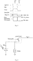
- A characteristic of operating at DC (0 Mbps) is where a command can be issued optically by control circuitry via an optical transmitter. In such an instance the receiver in idle mode may be receiving a DC light level and then must respond without fail to the first bit of a command signal data stream sent at any arbitrary time within a wide received optical power range. The conversion of optical light into a voltage is usually implemented using a transimpedance amplifier (TIA). If the dynamic range of the received light power is wide then a TIA with automatic gain control (AGC) is needed to reduce the gain for higher received light power. The use of a fully differential TIA is preferred for noise and electromagnetic interference (EMI) immunity. A photodiode has a single ended current output, and a fully differential TIA outputs a pseudo differential signal, as illustrated by
Fig. 1 . Creating an accurate comparator reference point for a pseudo differential signal at high speed instantaneously is difficult. Using a fully differential signal into a comparator ensures that the pulse width distortion (PWD) is low, which is needed for DC to multiple MHz frequency applications. - The invention is therefore directed towards achieving a fully differential signal in a simple and effective manner.
- Reference [1] describes an optical receiver that removes the DC photocurrent by feeding back the differential TIA output via an error amplifier to generate a low frequency DC rejection current. This includes a differential TIA and regulated gate cascode (RGC) but does not have an AGC. This approach does not appear to be suitable for a DC application because the differential signal is generated by feeding back the TIA outputs via an error amplifier which adds a significant lag before the differential signal is correctly generated.
- The approach of Reference [2] includes a differential TIA. As the peak detector is responding to the output voltage there is significant delay before a fully differential signal is created. Hence, this approach would not be suitable for DC applications where first bit PWD is specified.
- The following documents describe optical receivers:
- QUADIR NASIR ABDUL ET AL: "An inductorless linear optical receiver for 20Gbaud/s (40Gb/s) PAM-4 modulation using 28nm CMOS" 2014 IEEE INTERNATIONAL SYMPOSIUM ON CIRCUITS AND SYSTEMS (ISCAS), IEEE, 1 June 2014 (2014-06-01) pages 2473-2476.
- CHEN W-Z ET AL: "A 1.8-V 10-Gb/s Fully Integrated CMOS Optical Receiver Analog Front-End", IEEE JOURNAL OF SOLID-STATE CIRCUITS, IEEE SERVICE CENTER, PISCATAWAY, NJ, USA, vol. 40, no. 6, 1 June 2005 (2005-06-01), pages 1388-1396.
-
US6307660 B1 (CORDELL ROBERT ROGER [US] ET AL ). - PETER OSSIEUR ET AL: "A 10Gb/s Linear Burst-Mode Receiver ins 0.25 mum SiGe:C BiCMOS", IEEE JOURNAL OF SOLID-STATE CIRCUITS, IEEE SERVICE CENTER, PISCATAWAY, NJ, USA, vol. 48, no. 2, 1February 2013 (2013-02-01), pages 381-390.
- We describe an optical receiver comprising a differential TIA linked with a photodiode providing a current sense signal, wherein the receiver comprises a first cascode circuit (configured to provide to the TIA a sense signal as a sense TIA input (ISig_tia) and a circuit configured to provide to the TIA a proportion of a maximum sense signal as a proportion TIA input (Idark_tia, IpeakDet_2). There may be a replica circuit, and the first cascode circuit is configured to provide to the replica circuit a copy (Icopy) of the sense signal, based on replicating the TIA load, and the replica circuit is configured to provide a signal from which the proportion TIA input is derived. There may be a peak detector to peak detect said signal from the replica circuit, and the peak detector provides directly (Ipeak-Det_2) or indirectly (Ipeak_Det, Idark_tia) said proportion TIA input.
- The replica circuit may comprise a replica amplifier, a dummy transimpedance load, and a transconductance block. In one embodiment, the peak detector comprises a transconductance block.
- In one embodiment, the differential TIA gain is regulated with an automatic gain control AGC loop. In one embodiment, the cascode circuit is a regulated gate cascode RGC circuit.
- In one embodiment, the cascode circuit is biased with a bias current.
- In one embodiment, the peak detector is configured to generate a received signal strength indicator. Preferably, the receiver comprises a transconductance block driven by the peak detector output, and a received signal strength indicator is an output of the transconductance block.
- In one embodiment, the photodiode is a monolithic integrated photodiode.
- In one embodiment, the peak detector provides the proportion TIA input (IpeakDet_2) directly into an AGC within the TIA .
- In one embodiment, the peak detector comprises a transconductance component to provide a current sink signal (IpeakDet) for said second cascode circuit, configured to provide the proportion TIA input (Idark_tia).
- In one embodiment, the cascode circuits are configured to provide the proportion TIA input as half of said maximum sense signal. Preferably, the peak detector is configured to use a replicated current signal to generate half the maximum received current, and the second cascode circuit is arranged to produce a fully differential output voltage for incoming received light.
- In one embodiment, the first cascode circuitis arranged to provide a generated half the maximum received current signal as a current source to the positive input to the differential TIA or as a current sink to the negative input to the differential TIA, to produce a fully differential output voltage for incoming received light.
- In one embodiment, the receiver further comprises a dark photodiode or an equivalent element, and said second cascode circuit is connected to receive a signal (Idark) from said dark photodiode to provide the proportion TIA input.
- In one embodiment, said AGC configured to use positive and negative TIA outputs (TIA_plus, TIA_minus) as feedback signals to dynamically modify its gain.
- Preferably, the receiver further comprises a pseudo differential to differential amplifier connected at its input to an output of the TIA, said amplifier being configured to produce a fully differential output voltage for incoming received light.
- In one embodiment, the TIA is configured to use said pseudo differential to differential amplifier output signals (Diff_plus, Diff_minus) to dynamically adjust the AGC gain using feedback control.
- An electronic device comprising a processing circuit and an optical receiver of any embodiment.
- We also describe a receiver comprising a differential TIA linked with a transducer providing a current sense signal, wherein the receiver is configured to provide to the TIA a sense signal as a first input and a second input which is a proportion of the maximum sense signal.
- In one embodiment, the second input is half of said maximum sense signal.
- In one embodiment, the inputs to the TIA are via cascode circuits.
- In one embodiment, the TIA is configured to provide a copy or replica of the sense signal, based on replicating the TIA load, to a replica circuit to provide said second input.
- In one embodiment, the receiver comprises a peak detector to peak detect the sense signal copy.
- In one embodiment, the peak detector comprises a transconductance component to provide a current signal for the second input to the TIA.
- In one embodiment, the replicated current is used to generate half the maximum received current, which is connected into an input of the differential TIA via a cascode circuit, which will produce a fully differential output voltage for incoming received light.
- In one embodiment, the copy signal is connected as a current source to the positive input to the differential TIA, or as a current sink to the negative input of the differential TIA, via a cascode circuit to produce a fully differential output voltage for incoming received light.
- In one embodiment, the transducers comprise one or more photodiodes.
- In one embodiment, a dark photodiode or an equivalent element is connected to the second input of the differential TIA via another cascode circuit.
- In one embodiment, the sense signal is an input received current which is replicated, with use of a replica amplifier, a dummy transimpedance load and a transconductance block.
- In one embodiment, the maximum received current is generated with a peak detector and a transconductance block.
- In one embodiment, the differential TIA gain is regulated with an AGC loop.
- In one embodiment, the cascode circuit is a RGC circuit.
- In one embodiment, the cascode circuit is biased with a bias current.
- In one embodiment, a peak detector is used to generate a received signal strength indicator.
- In one embodiment, the output received signal strength indicator is the output of another transconductance block which is driven by the peak detector output
- In one embodiment, a transconductance circuit, where it is included, comprises:
- a first current sink with low transconductance and good accuracy for low output currents; and
- a second current sink with a high transconductance and a wide dynamic range.
- In one embodiment, the transconductance circuit comprises a source follower and a current sink for the source follower, in which the input is linked with the gate of the source follower and the first current sink. In one embodiment, the current sinks are configured so that at low input voltage only the low first current sink is on. In one embodiment, the source follower and the current sinks are configured so that a gate-source voltage drop across the source follower ensures that the second current sink is off until a point during which the input voltage increases at which the second current sink is switched on.
- In one embodiment, in the transconductance circuit the sizing of the first and second current sinks dictates the accuracy at lower voltage and range at the high voltage, and helps to linearize the output current over the input voltage range.
- In one embodiment, in the transconductance circuit each of the current sinks is a NMOS or a PMOS MOSFET device or a PNP or an NPN transistor.
- In one embodiment, in the transconductance circuit a plurality of devices with low to high transconductances are connected in parallel.
- In another aspect, we describe an electronic device comprising a processing circuit and a receiver as defined above in any embodiment.
- The invention will be more clearly understood from the following description of some embodiments thereof, given by way of example only with reference to the accompanying drawings in which:-
-
Fig. 1 is a set of plots to illustrate background to the invention, as set out above; -
Fig. 2 is a circuit diagram of an optical receiver of the invention; -
Fig. 3 is a set of plots for operation of the optical receiver; -
Fig. 4 is a diagram showing the cascode arrangement in more detail; -
Fig. 5 is a diagram of a transconductance circuit used in the receiver in some embodiments; -
Figs. 6 and7 are circuit diagrams of alternative optical receivers of the invention; and -
Fig. 8 is a series of plots for these receivers. - Referring to
Fig. 2 anoptical receiver 1 comprises a signal photodiode (PD) 2, adark PD 3, and adifferential TIA 4. There arecascode circuits replica circuit 10, and apeak detector circuit 11. The output from the series combination ofreplica circuit 10, and apeak detector circuit 11 is provided to theTIA 4 as IpeakDet, which creates a reference when added to Idark to produce Idark_tia which creates a fully differential TIA output when compared to the data signal Isig_tia. - The signal input to the
TIA 4 is via thecascode device 5 which: - receives a Vcas_sig_gate control signal,
- receives the
PD 2 signal, Isig, - receives a copied current Icopy, from the
replica circuit 10, - delivers a signal Isig_tiato the
TIA 4, - delivers a signal Icopy_tia to a replica load in the
TIA 4. - The reference input to the
TIA 4 is via thecascode device 6 which: - receives a control input Vcas_dark_gate,
- receives the
PD 3 reference signal Idark, - receives a reference signal IpeakDet from the
peak detector 11 and delivers a signal Idark tia to theTIA 4, which is a sum of Idark and IpeakDet. - The
peak detector 11 receives an input from thereplica circuit 10, and provides a feed-forward signal to the transconductance circuit (tc) tc2. This feed forward signal causes the circuit tc2 to produce an output IpeakDet, which is an input signal to theTIA 4, via thecascode device 6. This feedforward current creates a fully differential TIA output in combination with other inputs. Feed forward control is beneficial because of its speed in taking predefined action depending on the strength of the sense signal, which is particularly relevant in a burst mode receiver application. - In more detail, the
signal receiving photodiode 2 and thedark photodiode 3 are both connected to thecascode circuits differential TIA 4 whose gain can be regulated with an AGC control loop. A copy of the signal current is generated by thereplica circuitry 10, and is used by thepeak detector circuit 11 to output half the maximum input signal current. Thepeak detector circuit 11 output is connected to the dark (or minus) (in an alternative embodiment can be connected to the active side) side of thedifferential TIA 4. As illustrated inFig. 3 supplying a differential TIA with a signal and dark current in this manner produces a fully differential output signal. - Advantageously, the
TIA 4 receives a proportion TIA input which is half of the maximum signal, rather than for example being zero. This achieves a fully differential output. - The
differential TIA 4 input signal current (Isig_tia) is regenerated by thecascode circuit 5, where the gate source voltage is copied in thereplica circuit 10 with a replica amplifier (Amp) and transconductance block tc1 produces a replica of the signal current (Icopy) sinked from a replica load in theTIA 4 by Icopy_tia. - The cascode devices 5(a) and 5(b) are used to produce a copied current Icopy. If the gate, source and drain voltages of the cascode device 5(a) are equal to corresponding voltages of the cascode device 5(b) then the current will be the same through both devices. The gate voltage Vcas_sig_gate is common to both devices. The Amp and transconductance block tc1 of the
replica circuit 10 ensure that the source voltages VSA and VSB are the same, and the replica load input to the TIA 4(which is the same as the plus input) ensures that the drain voltage VDA and VDB will be the same if Icopy is the same as Isig. - The output voltage of the Amp in the
replica circuit 10 is peak detected by thepeak detector circuit 11, to output half the maximum received current (IpeakDet) by using a transconductance block tc2 which is half the size of the transconductance block tc1. This current IpeakDet equals half of maximum Isig_tia and is connected to the minus (or dark) side of the differential TIA via asecond cascode device 6, as shown inFig. 2 . The Idark_tia current is equal to the sum of thePD 3 reference Idark and the peak detector current IpeakDet. - The benefit of providing to the TIA 4 a replica load input is that it helps to provide a stable loop for the
replica circuitry 10 to reproduce the sense signal. The benefit of providing to the TIA a sense signal and a signal which is a fixed proportion of a maximum sense signal, is that this architecture produces a fully differential output TIA signal which is generated with minimum delay. It is because of this reason that this architecture is suitable for DC to multiple megabits per second (Mbps) applications. It has the advantage of processing the signal at the front end so that the bandwidth of thedifferential TIA 4 can be reduced for a low power receiver, and if an AGC was implemented with the TIA it would have limited implications on this architecture. - An additional aspect is that the peak detector output voltage can drive another (or multiple) transconductance block(s) tc3 to produce a Received Signal Strength Indication (RSSI) current IRSSI_OUT. If the transconductance block tc3 equals tc1, then this current is an accurate copy of the received photodiode current.
-
Fig. 4 shows how a static bias current can be used in a cascode circuit to enhance thecascode circuit 5 to improve speed, where Isig_tia = Isig + Ibias. Likewise, this bias current would be symmetrically used in the dark cascode to enhance thecircuit 6, and as a consequence its content must be removed from the peak detector current IpeakDet, in order for the receiver to output an accurate differential signal. - Referring to
Fig. 5 a transconductance circuit is illustrated for one or more of the components tc1, tc2, or tc3. This transconductance circuit comprises asource follower 102, acurrent sink 103 for the source follower, a low gmcurrent sink 104, and a high gmcurrent sink 105. The actual gm are not important, the important point being that thesink 105 has a higher gm that thesink 104. - This transconductance circuit improves the dynamic range of a single current sink, to improve the accuracy at low output currents and ensure it has the dynamic range to output higher currents if required.
- The manner in which the two
current sinks components current sink 104, and a high gmcurrent sink 105 in one circuit. At low VIN only the low gm device 4 is on, as the gate source voltage drop across the source follower (102) ensures that the high gm device (105) is off. As the VIN increases the high gm device 105 is switched on. The sizing of the low gm and high gm devices 4 and 5 dictate the accuracy at lower voltage and range at the high voltage, and helps to linearize the output current over the VIN range. - The
components current sinks sink 105 turns on later. Such a voltage drop may be provided by another means such as a combination of a resistor with a current source/sink, with the use of an amplifier to buffer the input from any current dissipation. - In various embodiments, the transconductance circuit which is used may have at least two current sinks. One sink is a single current sink which is sized to have low transconductance and to have good accuracy for low output currents, but would have a poor dynamic range. The other is a single current sink sized to have high gm and a wide dynamic range but poor accuracy for low output current. The
transconductance circuit 1 combines both of these current sinks into one circuit to achieve high accuracy for low output current, a wide dynamic range for high current, and improved the linearity across the range of output currents. - It will be appreciated that the transconductance circuit improves the dynamic range (due to the high gm current device), accuracy and tolerance to mismatch of the output current versus a single transconductance current sink (due to the low gm current device).
- In the transconductance circuit the NMOS devices may be replaced with PMOS devices, so the output transconductance current sinks are now transconductance current sources. Also, the NMOS or PMOS MOSFET devices may be replaced with NPN or PNP bipolar transistors creating bipolar based output transconductance current sources or current sinks.
- Also, the
optical receiver 1 achieves low EMI because of the differential architecture of the TIA and subsequent stages. Another reason is that the signal processing is implemented at the front end, which allows the reduction of the TIA bandwidth in burst mode applications to filter out high frequency noise. - An
optical receiver 100 of another embodiment is shown inFig. 6 . Like parts are given the same reference numerals. - In the
circuit 100 there is an additional proportion TIA input to thedifferential TIA 4, a signal IpeakDet_2, from thetransconductance circuit 12. This current is a proportion of the maximum sense signal. This signal provides a feed forward current to the automatic gain control (AGC)block 13. In this case a second or more inputs, which are a proportion of the maximum sense signal are provided to the TIA. - In more detail, the output of the
transconductance circuit 12 is used as an input to anAGC block 13 which is incorporated in the differential TIA. Known TIAs include such AGC blocks, the difference here being the connection to it from thetransconductance circuit 12. This signal, a third input current (IpeakDet_2), is a proportion of the maximum sense signal. This can be used to speed up the AGC using feed forward control to adjust the approximate optimal gain of the differential TIA in a pre-defined manner. TheAGC 13 may use the TIA outputs TIA_plus and TIA_minus signals to dynamically adjust the AGC gain using feedback control, to attain the required output amplitude. - The main advantage of this embodiment is that for high received power the
AGC 13 can quickly achieve the required differential TIA gain via feedforward control as to improve pulse width distortion (PWD) of the received data. This embodiment can be used to reduce the variation of the settling time of the AGC over process, temperature and voltage. - An alternative
optical receiver 200, is shown inFig. 7 . Again, parts similar to those of the other embodiments are given the same reference numerals. - Again, there is a proportion TIA input to the differential TIA where it's current is a proportion of the maximum sense signal.
- In the
Fig. 2 embodiment the proportion TIA input (Idark_tia) is used to produce a fully differential output voltage for incoming received light as the output of thepeak detector 11 was fed into thesecond cascode device 6. - This is not the case in the optical receiver 200 (
Fig. 7 ) embodiment as a pseudo differential todifferential amplifier 14 is now used to produce a fully differential output voltage for incoming received light. This proportion TIA input (IpeakDet_2) to the differential TIA is used as an input to the automatic gain control (AGC)block 13 which is incorporated in the differential TIA. This input current (IpeakDet_2) is a proportion of the maximum sense signal. This can be used to speed up the AGC using feed forward control to adjust the approximate optimal gain of the differential TIA in a pre-defined manner. - The AGC may use the pseudo differential to
differential amplifier 14 outputs Diff_plus and Diff_minus signals to dynamically adjust the AGC gain using feedback control. -
Fig. 8 is a plot of the signals in thecircuit 200, where the TIA output is a pseudo differential signal, and the differential signal is outputted from the pseudo differential todifferential amplifier 14. Again similar to the embodiment ofFig. 6 ; the same advantages apply here. - An extra advantage of this embodiment is that the total accuracy of the front end maximum current sense circuitry may be relaxed depending on the accuracy needed for the feed-forward control of the AGC. The mismatch of devices and variation over temperature no longer have a large impact on PWD of the receiver output.
- The invention is not limited to the embodiments described but may be varied in construction and detail. For example, the current signal may not represent a light signal, but represents another measurable signal from a transducer. The photodiode may be discrete or a monolithic integrated photodiode. The receiver may operate with transducers other than photodiodes
| [1] | Title: | "A transimpedance amplifier with DC-coupled differential photodiode current sensing for wireless optical communications" |
| Authors: | Bahram Zand, Khoman Phang, and David A. Johns. | |
| Published: | IEEE Conference on Custom Integrated Circuits, 2001, Pages: 455 - 458. | |
| [2] | Title: | "High-speed, Burst-Mode, Packet-Capable Optical Receiver and Instantaneous Clock Recovery for Optical Bus Operation" |
| Authors: | Yusuke Ota, Robert G. Swartz, Vance D. Archer 111, Steven K. Korotky, Mihai Banu, and Alfred E. Dunlop. | |
| Published: | JOURNAL OF LIGHTWAVE TECHNOLOGY, VOL. 12, NO. 2, FEBRUARY 1994, Pages 325- 331. | |
| Patent: | | |
| Filing date | Aug 22, 1994 |
Claims (15)
- An optical receiver comprising:a differential TIA (4) linked with a photodiode (2, 3) providing a current sense signal,a first cascode circuit (5(a), 5(b)) configured to provide to the TIA (4) a sense signal as a sense TIA input (Isig_tia), anda circuit configured to provide to the TIA (4) a proportion of a maximum sense signal as a proportion TIA input (Idark_tia, IpeakDet_2),a replica circuit (10), wherein the first cascode circuit (5(a), 5(b)) is configured to provide to the replica circuit (10) a copy (Icopy) of the sense signal, based on replicating the TIA load, and said replica circuit is configured to provide a signal from which said proportion TIA input is derived, anda peak detector (11) to peak detect said signal from the replica circuit (10), and the peak detector provides directly (Ipeak-Det_2) or indirectly (IpeakDet, Idark_tia) said proportion TIA input.
- An optical receiver as claimed in any of claim 1, wherein the replica circuit (10) comprises a replica amplifier (Amp), a dummy transimpedance load, and a transconductance block (tc1).
- An optical receiver as claimed in claims 1 or 2, wherein the peak detector (11) comprises a transconductance block (tc2).
- An optical receiver as claimed in any preceding claim, wherein the differential TIA gain is regulated with an automatic gain control AGC loop.
- An optical receiver as claimed in any preceding claim, wherein the cascode circuit (5, 6) is a regulated gate cascode RGC circuit.
- An optical receiver as claimed in any preceding claim, wherein the cascode circuit (5, 6) is biased with a bias current.
- An optical receiver as claimed in in any preceding claim, wherein the peak detector (11) is configured to generate a received signal strength indicator.
- An optical receiver as claimed in any preceding claim, wherein the receiver comprises a transconductance block (12) driven by the peak detector (11) output, and a received signal strength indicator is an output of the transconductance block (12).
- An optical receiver as claimed in any preceding claim, wherein the photodiode is a monolithic integrated photodiode.
- An optical receiver as claimed in any preceding claim, wherein the peak detector provides the proportion TIA input (IpeakDet_2) directly into an AGC within the TIA (4).
- An optical receiver as claimed in any preceding claim, wherein the peak detector (11) comprises a transconductance component to provide a current sink signal (IpeakDet) for said second cascode circuit (6), configured to provide the proportion TIA input (Idark_tia), and optionally the cascode circuits (6(a), 6(b)) are configured to provide the proportion TIA input as half of said maximum sense signal, and optionally the peak detector (10) is configured to use a replicated current signal to generate half the maximum received current, and the second cascode circuit (6) is arranged to produce a fully differential output voltage for incoming received light.
- An optical receiver as claimed in claim 11, wherein the first cascode circuit (5) is arranged to provide a generated half the maximum received current signal as a current source to the positive input to the differential TIA or as a current sink to the negative input to the differential TIA, to produce a fully differential output voltage for incoming received light, and optionally the receiver further comprises a dark photodiode (3) or an equivalent element, and said second cascode circuit (6) is connected to receive a signal (Idark) from said dark photodiode to provide the proportion TIA input.
- An optical receiver as claimed in either of claims 11 or 12, wherein said AGC (13) is configured to use positive and negative TIA outputs (TIA_plus,TIA_minus) as feedback signals to dynamically modify its gain.
- An optical receiver as claimed in any preceding claim, wherein the receiver further comprises a pseudo differential to differential amplifier (14) connected at its input to an output of the TIA (4), said amplifier being configured to produce a fully differential output voltage for incoming received light, and optionally the TIA (4) is configured to use said pseudo differential to differential amplifier (14) output signals (Diff_plus, Diff_minus) to dynamically adjust the AGC gain using feedback control.
- An electronic device comprising a processing circuit and an optical receiver as claimed in any preceding claim.
Applications Claiming Priority (2)
| Application Number | Priority Date | Filing Date | Title |
|---|---|---|---|
| EP15185217 | 2015-09-15 | ||
| PCT/EP2016/071528 WO2017046068A1 (en) | 2015-09-15 | 2016-09-13 | An optical receiver with a cascode front end |
Publications (2)
| Publication Number | Publication Date |
|---|---|
| EP3350945A1 EP3350945A1 (en) | 2018-07-25 |
| EP3350945B1 true EP3350945B1 (en) | 2019-11-06 |
Family
ID=54151103
Family Applications (1)
| Application Number | Title | Priority Date | Filing Date |
|---|---|---|---|
| EP16763848.5A Active EP3350945B1 (en) | 2015-09-15 | 2016-09-13 | An optical receiver with a cascode front end |
Country Status (4)
| Country | Link |
|---|---|
| US (1) | US20200235823A1 (en) |
| EP (1) | EP3350945B1 (en) |
| CN (1) | CN108141286A (en) |
| WO (1) | WO2017046068A1 (en) |
Families Citing this family (4)
| Publication number | Priority date | Publication date | Assignee | Title |
|---|---|---|---|---|
| CN109560879B (en) * | 2017-09-27 | 2021-06-22 | 敦宏科技股份有限公司 | Optical receiving circuit with dark current correction function and dark current correction method thereof |
| JP7467298B2 (en) * | 2020-09-16 | 2024-04-15 | 株式会社東芝 | Protection Circuit |
| US11843418B2 (en) * | 2021-09-16 | 2023-12-12 | Cisco Technology, Inc. | DC and offset cancellation for fully differential optical receiver |
| FR3131813B1 (en) * | 2022-01-13 | 2024-01-12 | St Microelectronics Alps Sas | Receiver device, system, reception method and light signal communication method. |
Family Cites Families (7)
| Publication number | Priority date | Publication date | Assignee | Title |
|---|---|---|---|---|
| CA2106439A1 (en) | 1992-11-13 | 1994-05-14 | Yusuke Ota | Burst mode digital data receiver |
| JP2656734B2 (en) * | 1994-09-12 | 1997-09-24 | 宮城日本電気株式会社 | Optical receiving circuit |
| US6307660B1 (en) * | 1997-01-28 | 2001-10-23 | Tellium, Inc. | Optical receiver particularly useful for a multi-wavelength receiver array |
| US5793230A (en) * | 1997-02-26 | 1998-08-11 | Sandia Corporation | Sensor readout detector circuit |
| US7986926B2 (en) * | 2006-09-27 | 2011-07-26 | Silicon Laboratories Inc. | Integrating an FM transmitter into a cellular telephone |
| KR102286595B1 (en) * | 2014-11-14 | 2021-08-05 | 한국전자통신연구원 | A RGC type burst-mode optic pre-amplifier having wide linear input range |
| US10333472B2 (en) * | 2015-09-15 | 2019-06-25 | Firecomms Limited | Optical receiver |
-
2016
- 2016-09-13 US US15/758,847 patent/US20200235823A1/en not_active Abandoned
- 2016-09-13 WO PCT/EP2016/071528 patent/WO2017046068A1/en active Application Filing
- 2016-09-13 CN CN201680061266.4A patent/CN108141286A/en active Pending
- 2016-09-13 EP EP16763848.5A patent/EP3350945B1/en active Active
Non-Patent Citations (1)
| Title |
|---|
| None * |
Also Published As
| Publication number | Publication date |
|---|---|
| CN108141286A (en) | 2018-06-08 |
| EP3350945A1 (en) | 2018-07-25 |
| US20200235823A1 (en) | 2020-07-23 |
| WO2017046068A1 (en) | 2017-03-23 |
Similar Documents
| Publication | Publication Date | Title |
|---|---|---|
| US6037841A (en) | Impedance matched CMOS transimpedance amplifier for high-speed fiber optic communications | |
| US6593810B2 (en) | 2.5 Gigabits-per-second transimpedance amplifier | |
| US8964825B2 (en) | Analog signal current integrators with tunable peaking function | |
| CN107835054B (en) | Transimpedance amplifier for high-speed optical communication based on linear modulation | |
| EP3350945B1 (en) | An optical receiver with a cascode front end | |
| US10484213B2 (en) | DC offset cancellation and crosspoint control circuit | |
| WO2009055035A2 (en) | High sensitivity two-stage amplifier | |
| US10333472B2 (en) | Optical receiver | |
| US8599966B2 (en) | Coupling system for data receivers | |
| KR100723535B1 (en) | Receiver for reducing intersymbol interference of channel and for compensating signal gain loss | |
| EP0868038B1 (en) | Burst mode digital optical receiver | |
| US6914479B1 (en) | Differential amplifier with DC offset cancellation | |
| JP6661057B1 (en) | Limiting amplifier circuit | |
| EP0382373B1 (en) | Nonlinear noninverting transimpedance amplifier | |
| US7348809B2 (en) | Input buffer | |
| US4817208A (en) | Fiber optic receiver | |
| CN113300675B (en) | Burst mode optical receiver transimpedance amplifier circuit with reduced settling time | |
| JPH1084228A (en) | Optical transmitting device | |
| US10992390B2 (en) | Circuit for multiplexing MON pin of receiver optical sub-assembly for optical communication | |
| US7088174B2 (en) | Offset cancellation and slice adjust amplifier circuit | |
| EP2870696B1 (en) | Driver circuit | |
| US9673815B2 (en) | Driver circuit | |
| JP2007036329A (en) | Amplifier circuit and transimpedance amplifier | |
| US7372328B2 (en) | Amplification circuit for driving a laser signal | |
| CN116805890A (en) | Optoelectronic component |
Legal Events
| Date | Code | Title | Description |
|---|---|---|---|
| STAA | Information on the status of an ep patent application or granted ep patent |
Free format text: STATUS: THE INTERNATIONAL PUBLICATION HAS BEEN MADE |
|
| PUAI | Public reference made under article 153(3) epc to a published international application that has entered the european phase |
Free format text: ORIGINAL CODE: 0009012 |
|
| STAA | Information on the status of an ep patent application or granted ep patent |
Free format text: STATUS: REQUEST FOR EXAMINATION WAS MADE |
|
| 17P | Request for examination filed |
Effective date: 20180410 |
|
| AK | Designated contracting states |
Kind code of ref document: A1 Designated state(s): AL AT BE BG CH CY CZ DE DK EE ES FI FR GB GR HR HU IE IS IT LI LT LU LV MC MK MT NL NO PL PT RO RS SE SI SK SM TR |
|
| AX | Request for extension of the european patent |
Extension state: BA ME |
|
| DAV | Request for validation of the european patent (deleted) | ||
| DAX | Request for extension of the european patent (deleted) | ||
| GRAP | Despatch of communication of intention to grant a patent |
Free format text: ORIGINAL CODE: EPIDOSNIGR1 |
|
| STAA | Information on the status of an ep patent application or granted ep patent |
Free format text: STATUS: GRANT OF PATENT IS INTENDED |
|
| INTG | Intention to grant announced |
Effective date: 20190604 |
|
| GRAS | Grant fee paid |
Free format text: ORIGINAL CODE: EPIDOSNIGR3 |
|
| GRAA | (expected) grant |
Free format text: ORIGINAL CODE: 0009210 |
|
| STAA | Information on the status of an ep patent application or granted ep patent |
Free format text: STATUS: THE PATENT HAS BEEN GRANTED |
|
| AK | Designated contracting states |
Kind code of ref document: B1 Designated state(s): AL AT BE BG CH CY CZ DE DK EE ES FI FR GB GR HR HU IE IS IT LI LT LU LV MC MK MT NL NO PL PT RO RS SE SI SK SM TR |
|
| REG | Reference to a national code |
Ref country code: GB Ref legal event code: FG4D |
|
| REG | Reference to a national code |
Ref country code: CH Ref legal event code: EP Ref country code: AT Ref legal event code: REF Ref document number: 1200226 Country of ref document: AT Kind code of ref document: T Effective date: 20191115 |
|
| REG | Reference to a national code |
Ref country code: IE Ref legal event code: FG4D |
|
| REG | Reference to a national code |
Ref country code: DE Ref legal event code: R096 Ref document number: 602016023860 Country of ref document: DE |
|
| REG | Reference to a national code |
Ref country code: NL Ref legal event code: MP Effective date: 20191106 |
|
| REG | Reference to a national code |
Ref country code: LT Ref legal event code: MG4D |
|
| PG25 | Lapsed in a contracting state [announced via postgrant information from national office to epo] |
Ref country code: PT Free format text: LAPSE BECAUSE OF FAILURE TO SUBMIT A TRANSLATION OF THE DESCRIPTION OR TO PAY THE FEE WITHIN THE PRESCRIBED TIME-LIMIT Effective date: 20200306 Ref country code: FI Free format text: LAPSE BECAUSE OF FAILURE TO SUBMIT A TRANSLATION OF THE DESCRIPTION OR TO PAY THE FEE WITHIN THE PRESCRIBED TIME-LIMIT Effective date: 20191106 Ref country code: LV Free format text: LAPSE BECAUSE OF FAILURE TO SUBMIT A TRANSLATION OF THE DESCRIPTION OR TO PAY THE FEE WITHIN THE PRESCRIBED TIME-LIMIT Effective date: 20191106 Ref country code: SE Free format text: LAPSE BECAUSE OF FAILURE TO SUBMIT A TRANSLATION OF THE DESCRIPTION OR TO PAY THE FEE WITHIN THE PRESCRIBED TIME-LIMIT Effective date: 20191106 Ref country code: BG Free format text: LAPSE BECAUSE OF FAILURE TO SUBMIT A TRANSLATION OF THE DESCRIPTION OR TO PAY THE FEE WITHIN THE PRESCRIBED TIME-LIMIT Effective date: 20200206 Ref country code: PL Free format text: LAPSE BECAUSE OF FAILURE TO SUBMIT A TRANSLATION OF THE DESCRIPTION OR TO PAY THE FEE WITHIN THE PRESCRIBED TIME-LIMIT Effective date: 20191106 Ref country code: LT Free format text: LAPSE BECAUSE OF FAILURE TO SUBMIT A TRANSLATION OF THE DESCRIPTION OR TO PAY THE FEE WITHIN THE PRESCRIBED TIME-LIMIT Effective date: 20191106 Ref country code: NO Free format text: LAPSE BECAUSE OF FAILURE TO SUBMIT A TRANSLATION OF THE DESCRIPTION OR TO PAY THE FEE WITHIN THE PRESCRIBED TIME-LIMIT Effective date: 20200206 Ref country code: GR Free format text: LAPSE BECAUSE OF FAILURE TO SUBMIT A TRANSLATION OF THE DESCRIPTION OR TO PAY THE FEE WITHIN THE PRESCRIBED TIME-LIMIT Effective date: 20200207 Ref country code: NL Free format text: LAPSE BECAUSE OF FAILURE TO SUBMIT A TRANSLATION OF THE DESCRIPTION OR TO PAY THE FEE WITHIN THE PRESCRIBED TIME-LIMIT Effective date: 20191106 |
|
| PG25 | Lapsed in a contracting state [announced via postgrant information from national office to epo] |
Ref country code: IS Free format text: LAPSE BECAUSE OF FAILURE TO SUBMIT A TRANSLATION OF THE DESCRIPTION OR TO PAY THE FEE WITHIN THE PRESCRIBED TIME-LIMIT Effective date: 20200306 Ref country code: HR Free format text: LAPSE BECAUSE OF FAILURE TO SUBMIT A TRANSLATION OF THE DESCRIPTION OR TO PAY THE FEE WITHIN THE PRESCRIBED TIME-LIMIT Effective date: 20191106 Ref country code: RS Free format text: LAPSE BECAUSE OF FAILURE TO SUBMIT A TRANSLATION OF THE DESCRIPTION OR TO PAY THE FEE WITHIN THE PRESCRIBED TIME-LIMIT Effective date: 20191106 |
|
| PG25 | Lapsed in a contracting state [announced via postgrant information from national office to epo] |
Ref country code: AL Free format text: LAPSE BECAUSE OF FAILURE TO SUBMIT A TRANSLATION OF THE DESCRIPTION OR TO PAY THE FEE WITHIN THE PRESCRIBED TIME-LIMIT Effective date: 20191106 |
|
| PG25 | Lapsed in a contracting state [announced via postgrant information from national office to epo] |
Ref country code: EE Free format text: LAPSE BECAUSE OF FAILURE TO SUBMIT A TRANSLATION OF THE DESCRIPTION OR TO PAY THE FEE WITHIN THE PRESCRIBED TIME-LIMIT Effective date: 20191106 Ref country code: DK Free format text: LAPSE BECAUSE OF FAILURE TO SUBMIT A TRANSLATION OF THE DESCRIPTION OR TO PAY THE FEE WITHIN THE PRESCRIBED TIME-LIMIT Effective date: 20191106 Ref country code: RO Free format text: LAPSE BECAUSE OF FAILURE TO SUBMIT A TRANSLATION OF THE DESCRIPTION OR TO PAY THE FEE WITHIN THE PRESCRIBED TIME-LIMIT Effective date: 20191106 Ref country code: CZ Free format text: LAPSE BECAUSE OF FAILURE TO SUBMIT A TRANSLATION OF THE DESCRIPTION OR TO PAY THE FEE WITHIN THE PRESCRIBED TIME-LIMIT Effective date: 20191106 Ref country code: ES Free format text: LAPSE BECAUSE OF FAILURE TO SUBMIT A TRANSLATION OF THE DESCRIPTION OR TO PAY THE FEE WITHIN THE PRESCRIBED TIME-LIMIT Effective date: 20191106 |
|
| REG | Reference to a national code |
Ref country code: DE Ref legal event code: R097 Ref document number: 602016023860 Country of ref document: DE |
|
| REG | Reference to a national code |
Ref country code: AT Ref legal event code: MK05 Ref document number: 1200226 Country of ref document: AT Kind code of ref document: T Effective date: 20191106 |
|
| PG25 | Lapsed in a contracting state [announced via postgrant information from national office to epo] |
Ref country code: SM Free format text: LAPSE BECAUSE OF FAILURE TO SUBMIT A TRANSLATION OF THE DESCRIPTION OR TO PAY THE FEE WITHIN THE PRESCRIBED TIME-LIMIT Effective date: 20191106 Ref country code: SK Free format text: LAPSE BECAUSE OF FAILURE TO SUBMIT A TRANSLATION OF THE DESCRIPTION OR TO PAY THE FEE WITHIN THE PRESCRIBED TIME-LIMIT Effective date: 20191106 |
|
| PLBE | No opposition filed within time limit |
Free format text: ORIGINAL CODE: 0009261 |
|
| STAA | Information on the status of an ep patent application or granted ep patent |
Free format text: STATUS: NO OPPOSITION FILED WITHIN TIME LIMIT |
|
| 26N | No opposition filed |
Effective date: 20200807 |
|
| PG25 | Lapsed in a contracting state [announced via postgrant information from national office to epo] |
Ref country code: AT Free format text: LAPSE BECAUSE OF FAILURE TO SUBMIT A TRANSLATION OF THE DESCRIPTION OR TO PAY THE FEE WITHIN THE PRESCRIBED TIME-LIMIT Effective date: 20191106 Ref country code: SI Free format text: LAPSE BECAUSE OF FAILURE TO SUBMIT A TRANSLATION OF THE DESCRIPTION OR TO PAY THE FEE WITHIN THE PRESCRIBED TIME-LIMIT Effective date: 20191106 |
|
| PG25 | Lapsed in a contracting state [announced via postgrant information from national office to epo] |
Ref country code: IT Free format text: LAPSE BECAUSE OF FAILURE TO SUBMIT A TRANSLATION OF THE DESCRIPTION OR TO PAY THE FEE WITHIN THE PRESCRIBED TIME-LIMIT Effective date: 20191106 |
|
| REG | Reference to a national code |
Ref country code: CH Ref legal event code: PL |
|
| GBPC | Gb: european patent ceased through non-payment of renewal fee |
Effective date: 20200913 |
|
| REG | Reference to a national code |
Ref country code: BE Ref legal event code: MM Effective date: 20200930 |
|
| PG25 | Lapsed in a contracting state [announced via postgrant information from national office to epo] |
Ref country code: LU Free format text: LAPSE BECAUSE OF NON-PAYMENT OF DUE FEES Effective date: 20200913 |
|
| PG25 | Lapsed in a contracting state [announced via postgrant information from national office to epo] |
Ref country code: FR Free format text: LAPSE BECAUSE OF NON-PAYMENT OF DUE FEES Effective date: 20200930 |
|
| PG25 | Lapsed in a contracting state [announced via postgrant information from national office to epo] |
Ref country code: BE Free format text: LAPSE BECAUSE OF NON-PAYMENT OF DUE FEES Effective date: 20200930 Ref country code: CH Free format text: LAPSE BECAUSE OF NON-PAYMENT OF DUE FEES Effective date: 20200930 Ref country code: LI Free format text: LAPSE BECAUSE OF NON-PAYMENT OF DUE FEES Effective date: 20200930 Ref country code: IE Free format text: LAPSE BECAUSE OF NON-PAYMENT OF DUE FEES Effective date: 20200913 Ref country code: GB Free format text: LAPSE BECAUSE OF NON-PAYMENT OF DUE FEES Effective date: 20200913 |
|
| PG25 | Lapsed in a contracting state [announced via postgrant information from national office to epo] |
Ref country code: TR Free format text: LAPSE BECAUSE OF FAILURE TO SUBMIT A TRANSLATION OF THE DESCRIPTION OR TO PAY THE FEE WITHIN THE PRESCRIBED TIME-LIMIT Effective date: 20191106 Ref country code: MT Free format text: LAPSE BECAUSE OF FAILURE TO SUBMIT A TRANSLATION OF THE DESCRIPTION OR TO PAY THE FEE WITHIN THE PRESCRIBED TIME-LIMIT Effective date: 20191106 Ref country code: CY Free format text: LAPSE BECAUSE OF FAILURE TO SUBMIT A TRANSLATION OF THE DESCRIPTION OR TO PAY THE FEE WITHIN THE PRESCRIBED TIME-LIMIT Effective date: 20191106 |
|
| PG25 | Lapsed in a contracting state [announced via postgrant information from national office to epo] |
Ref country code: MK Free format text: LAPSE BECAUSE OF FAILURE TO SUBMIT A TRANSLATION OF THE DESCRIPTION OR TO PAY THE FEE WITHIN THE PRESCRIBED TIME-LIMIT Effective date: 20191106 Ref country code: MC Free format text: LAPSE BECAUSE OF FAILURE TO SUBMIT A TRANSLATION OF THE DESCRIPTION OR TO PAY THE FEE WITHIN THE PRESCRIBED TIME-LIMIT Effective date: 20191106 |
|
| P01 | Opt-out of the competence of the unified patent court (upc) registered |
Effective date: 20230413 |
|
| PGFP | Annual fee paid to national office [announced via postgrant information from national office to epo] |
Ref country code: DE Payment date: 20240819 Year of fee payment: 9 |