EP3349551A1 - A printed circuit board embedding a power die and a method for manufacturing said printed circuit board - Google Patents
A printed circuit board embedding a power die and a method for manufacturing said printed circuit board Download PDFInfo
- Publication number
- EP3349551A1 EP3349551A1 EP17151014.2A EP17151014A EP3349551A1 EP 3349551 A1 EP3349551 A1 EP 3349551A1 EP 17151014 A EP17151014 A EP 17151014A EP 3349551 A1 EP3349551 A1 EP 3349551A1
- Authority
- EP
- European Patent Office
- Prior art keywords
- printed circuit
- circuit board
- cavity
- power die
- dielectric fluid
- Prior art date
- Legal status (The legal status is an assumption and is not a legal conclusion. Google has not performed a legal analysis and makes no representation as to the accuracy of the status listed.)
- Granted
Links
Images


Classifications
-
- H—ELECTRICITY
- H05—ELECTRIC TECHNIQUES NOT OTHERWISE PROVIDED FOR
- H05K—PRINTED CIRCUITS; CASINGS OR CONSTRUCTIONAL DETAILS OF ELECTRIC APPARATUS; MANUFACTURE OF ASSEMBLAGES OF ELECTRICAL COMPONENTS
- H05K1/00—Printed circuits
- H05K1/18—Printed circuits structurally associated with non-printed electric components
- H05K1/182—Printed circuits structurally associated with non-printed electric components associated with components mounted in printed circuit boards [PCB], e.g. insert-mounted components [IMC]
- H05K1/185—Printed circuits structurally associated with non-printed electric components associated with components mounted in printed circuit boards [PCB], e.g. insert-mounted components [IMC] associated with components encapsulated in the insulating substrate of the PCBs; associated with components incorporated in internal layers of multilayer circuit boards
-
- H—ELECTRICITY
- H05—ELECTRIC TECHNIQUES NOT OTHERWISE PROVIDED FOR
- H05K—PRINTED CIRCUITS; CASINGS OR CONSTRUCTIONAL DETAILS OF ELECTRIC APPARATUS; MANUFACTURE OF ASSEMBLAGES OF ELECTRICAL COMPONENTS
- H05K1/00—Printed circuits
- H05K1/02—Details
- H05K1/14—Structural association of two or more printed circuits
- H05K1/145—Arrangements wherein electric components are disposed between and simultaneously connected to two planar printed circuit boards, e.g. Cordwood modules
-
- H—ELECTRICITY
- H05—ELECTRIC TECHNIQUES NOT OTHERWISE PROVIDED FOR
- H05K—PRINTED CIRCUITS; CASINGS OR CONSTRUCTIONAL DETAILS OF ELECTRIC APPARATUS; MANUFACTURE OF ASSEMBLAGES OF ELECTRICAL COMPONENTS
- H05K3/00—Apparatus or processes for manufacturing printed circuits
- H05K3/30—Assembling printed circuits with electric components, e.g. with resistors
- H05K3/32—Assembling printed circuits with electric components, e.g. with resistors electrically connecting electric components or wires to printed circuits
- H05K3/325—Assembling printed circuits with electric components, e.g. with resistors electrically connecting electric components or wires to printed circuits by abutting or pinching; Mechanical auxiliary parts therefor
-
- H—ELECTRICITY
- H05—ELECTRIC TECHNIQUES NOT OTHERWISE PROVIDED FOR
- H05K—PRINTED CIRCUITS; CASINGS OR CONSTRUCTIONAL DETAILS OF ELECTRIC APPARATUS; MANUFACTURE OF ASSEMBLAGES OF ELECTRICAL COMPONENTS
- H05K3/00—Apparatus or processes for manufacturing printed circuits
- H05K3/46—Manufacturing multilayer circuits
- H05K3/4697—Manufacturing multilayer circuits having cavities, e.g. for mounting components
-
- H—ELECTRICITY
- H10—SEMICONDUCTOR DEVICES; ELECTRIC SOLID-STATE DEVICES NOT OTHERWISE PROVIDED FOR
- H10W—GENERIC PACKAGES, INTERCONNECTIONS, CONNECTORS OR OTHER CONSTRUCTIONAL DETAILS OF DEVICES COVERED BY CLASS H10
- H10W76/00—Containers; Fillings or auxiliary members therefor; Seals
- H10W76/10—Containers or parts thereof
- H10W76/12—Containers or parts thereof characterised by their shape
- H10W76/15—Containers comprising an insulating or insulated base
- H10W76/153—Containers comprising an insulating or insulated base having interconnections in passages through the insulating or insulated base
-
- H—ELECTRICITY
- H10—SEMICONDUCTOR DEVICES; ELECTRIC SOLID-STATE DEVICES NOT OTHERWISE PROVIDED FOR
- H10W—GENERIC PACKAGES, INTERCONNECTIONS, CONNECTORS OR OTHER CONSTRUCTIONAL DETAILS OF DEVICES COVERED BY CLASS H10
- H10W76/00—Containers; Fillings or auxiliary members therefor; Seals
- H10W76/40—Fillings or auxiliary members in containers, e.g. centering rings
- H10W76/42—Fillings
- H10W76/45—Liquid fillings
-
- H—ELECTRICITY
- H10—SEMICONDUCTOR DEVICES; ELECTRIC SOLID-STATE DEVICES NOT OTHERWISE PROVIDED FOR
- H10W—GENERIC PACKAGES, INTERCONNECTIONS, CONNECTORS OR OTHER CONSTRUCTIONAL DETAILS OF DEVICES COVERED BY CLASS H10
- H10W76/00—Containers; Fillings or auxiliary members therefor; Seals
- H10W76/40—Fillings or auxiliary members in containers, e.g. centering rings
- H10W76/42—Fillings
- H10W76/47—Solid or gel fillings
-
- H—ELECTRICITY
- H10—SEMICONDUCTOR DEVICES; ELECTRIC SOLID-STATE DEVICES NOT OTHERWISE PROVIDED FOR
- H10W—GENERIC PACKAGES, INTERCONNECTIONS, CONNECTORS OR OTHER CONSTRUCTIONAL DETAILS OF DEVICES COVERED BY CLASS H10
- H10W90/00—Package configurations
- H10W90/401—Package configurations characterised by multiple insulating or insulated package substrates, interposers or RDLs
-
- H—ELECTRICITY
- H10—SEMICONDUCTOR DEVICES; ELECTRIC SOLID-STATE DEVICES NOT OTHERWISE PROVIDED FOR
- H10W—GENERIC PACKAGES, INTERCONNECTIONS, CONNECTORS OR OTHER CONSTRUCTIONAL DETAILS OF DEVICES COVERED BY CLASS H10
- H10W90/00—Package configurations
- H10W90/701—Package configurations characterised by the relative positions of pads or connectors relative to package parts
-
- H—ELECTRICITY
- H05—ELECTRIC TECHNIQUES NOT OTHERWISE PROVIDED FOR
- H05K—PRINTED CIRCUITS; CASINGS OR CONSTRUCTIONAL DETAILS OF ELECTRIC APPARATUS; MANUFACTURE OF ASSEMBLAGES OF ELECTRICAL COMPONENTS
- H05K1/00—Printed circuits
- H05K1/02—Details
- H05K1/0201—Thermal arrangements, e.g. for cooling, heating or preventing overheating
- H05K1/0203—Cooling of mounted components
- H05K1/0204—Cooling of mounted components using means for thermal conduction connection in the thickness direction of the substrate
- H05K1/0206—Cooling of mounted components using means for thermal conduction connection in the thickness direction of the substrate by printed thermal vias
-
- H—ELECTRICITY
- H05—ELECTRIC TECHNIQUES NOT OTHERWISE PROVIDED FOR
- H05K—PRINTED CIRCUITS; CASINGS OR CONSTRUCTIONAL DETAILS OF ELECTRIC APPARATUS; MANUFACTURE OF ASSEMBLAGES OF ELECTRICAL COMPONENTS
- H05K2201/00—Indexing scheme relating to printed circuits covered by H05K1/00
- H05K2201/01—Dielectrics
- H05K2201/0137—Materials
- H05K2201/0162—Silicon containing polymer, e.g. silicone
-
- H—ELECTRICITY
- H05—ELECTRIC TECHNIQUES NOT OTHERWISE PROVIDED FOR
- H05K—PRINTED CIRCUITS; CASINGS OR CONSTRUCTIONAL DETAILS OF ELECTRIC APPARATUS; MANUFACTURE OF ASSEMBLAGES OF ELECTRICAL COMPONENTS
- H05K2201/00—Indexing scheme relating to printed circuits covered by H05K1/00
- H05K2201/02—Fillers; Particles; Fibers; Reinforcement materials
- H05K2201/0203—Fillers and particles
- H05K2201/0242—Shape of an individual particle
- H05K2201/026—Nanotubes or nanowires
-
- H—ELECTRICITY
- H05—ELECTRIC TECHNIQUES NOT OTHERWISE PROVIDED FOR
- H05K—PRINTED CIRCUITS; CASINGS OR CONSTRUCTIONAL DETAILS OF ELECTRIC APPARATUS; MANUFACTURE OF ASSEMBLAGES OF ELECTRICAL COMPONENTS
- H05K2201/00—Indexing scheme relating to printed circuits covered by H05K1/00
- H05K2201/10—Details of components or other objects attached to or integrated in a printed circuit board
- H05K2201/10007—Types of components
- H05K2201/10166—Transistor
-
- H—ELECTRICITY
- H05—ELECTRIC TECHNIQUES NOT OTHERWISE PROVIDED FOR
- H05K—PRINTED CIRCUITS; CASINGS OR CONSTRUCTIONAL DETAILS OF ELECTRIC APPARATUS; MANUFACTURE OF ASSEMBLAGES OF ELECTRICAL COMPONENTS
- H05K2203/00—Indexing scheme relating to apparatus or processes for manufacturing printed circuits covered by H05K3/00
- H05K2203/03—Metal processing
- H05K2203/0307—Providing micro- or nanometer scale roughness on a metal surface, e.g. by plating of nodules or dendrites
-
- H—ELECTRICITY
- H05—ELECTRIC TECHNIQUES NOT OTHERWISE PROVIDED FOR
- H05K—PRINTED CIRCUITS; CASINGS OR CONSTRUCTIONAL DETAILS OF ELECTRIC APPARATUS; MANUFACTURE OF ASSEMBLAGES OF ELECTRICAL COMPONENTS
- H05K3/00—Apparatus or processes for manufacturing printed circuits
- H05K3/36—Assembling printed circuits with other printed circuits
- H05K3/366—Assembling printed circuits with other printed circuits substantially perpendicularly to each other
-
- H—ELECTRICITY
- H10—SEMICONDUCTOR DEVICES; ELECTRIC SOLID-STATE DEVICES NOT OTHERWISE PROVIDED FOR
- H10W—GENERIC PACKAGES, INTERCONNECTIONS, CONNECTORS OR OTHER CONSTRUCTIONAL DETAILS OF DEVICES COVERED BY CLASS H10
- H10W70/00—Package substrates; Interposers; Redistribution layers [RDL]
- H10W70/60—Insulating or insulated package substrates; Interposers; Redistribution layers
- H10W70/67—Insulating or insulated package substrates; Interposers; Redistribution layers characterised by their insulating layers or insulating parts
- H10W70/68—Shapes or dispositions thereof
- H10W70/682—Shapes or dispositions thereof comprising holes having chips therein
-
- H—ELECTRICITY
- H10—SEMICONDUCTOR DEVICES; ELECTRIC SOLID-STATE DEVICES NOT OTHERWISE PROVIDED FOR
- H10W—GENERIC PACKAGES, INTERCONNECTIONS, CONNECTORS OR OTHER CONSTRUCTIONAL DETAILS OF DEVICES COVERED BY CLASS H10
- H10W72/00—Interconnections or connectors in packages
- H10W72/071—Connecting or disconnecting
- H10W72/073—Connecting or disconnecting of die-attach connectors
- H10W72/07351—Connecting or disconnecting of die-attach connectors characterised by changes in properties of the die-attach connectors during connecting
-
- H—ELECTRICITY
- H10—SEMICONDUCTOR DEVICES; ELECTRIC SOLID-STATE DEVICES NOT OTHERWISE PROVIDED FOR
- H10W—GENERIC PACKAGES, INTERCONNECTIONS, CONNECTORS OR OTHER CONSTRUCTIONAL DETAILS OF DEVICES COVERED BY CLASS H10
- H10W72/00—Interconnections or connectors in packages
- H10W72/071—Connecting or disconnecting
- H10W72/073—Connecting or disconnecting of die-attach connectors
- H10W72/07351—Connecting or disconnecting of die-attach connectors characterised by changes in properties of the die-attach connectors during connecting
- H10W72/07352—Connecting or disconnecting of die-attach connectors characterised by changes in properties of the die-attach connectors during connecting changes in structures or sizes
-
- H—ELECTRICITY
- H10—SEMICONDUCTOR DEVICES; ELECTRIC SOLID-STATE DEVICES NOT OTHERWISE PROVIDED FOR
- H10W—GENERIC PACKAGES, INTERCONNECTIONS, CONNECTORS OR OTHER CONSTRUCTIONAL DETAILS OF DEVICES COVERED BY CLASS H10
- H10W72/00—Interconnections or connectors in packages
- H10W72/071—Connecting or disconnecting
- H10W72/073—Connecting or disconnecting of die-attach connectors
- H10W72/07351—Connecting or disconnecting of die-attach connectors characterised by changes in properties of the die-attach connectors during connecting
- H10W72/07354—Connecting or disconnecting of die-attach connectors characterised by changes in properties of the die-attach connectors during connecting changes in dispositions
-
- H—ELECTRICITY
- H10—SEMICONDUCTOR DEVICES; ELECTRIC SOLID-STATE DEVICES NOT OTHERWISE PROVIDED FOR
- H10W—GENERIC PACKAGES, INTERCONNECTIONS, CONNECTORS OR OTHER CONSTRUCTIONAL DETAILS OF DEVICES COVERED BY CLASS H10
- H10W72/00—Interconnections or connectors in packages
- H10W72/30—Die-attach connectors
-
- H—ELECTRICITY
- H10—SEMICONDUCTOR DEVICES; ELECTRIC SOLID-STATE DEVICES NOT OTHERWISE PROVIDED FOR
- H10W—GENERIC PACKAGES, INTERCONNECTIONS, CONNECTORS OR OTHER CONSTRUCTIONAL DETAILS OF DEVICES COVERED BY CLASS H10
- H10W72/00—Interconnections or connectors in packages
- H10W72/30—Die-attach connectors
- H10W72/321—Structures or relative sizes of die-attach connectors
- H10W72/325—Die-attach connectors having a filler embedded in a matrix
-
- H—ELECTRICITY
- H10—SEMICONDUCTOR DEVICES; ELECTRIC SOLID-STATE DEVICES NOT OTHERWISE PROVIDED FOR
- H10W—GENERIC PACKAGES, INTERCONNECTIONS, CONNECTORS OR OTHER CONSTRUCTIONAL DETAILS OF DEVICES COVERED BY CLASS H10
- H10W72/00—Interconnections or connectors in packages
- H10W72/30—Die-attach connectors
- H10W72/321—Structures or relative sizes of die-attach connectors
- H10W72/327—Multiple die-attach connectors having different sizes
-
- H—ELECTRICITY
- H10—SEMICONDUCTOR DEVICES; ELECTRIC SOLID-STATE DEVICES NOT OTHERWISE PROVIDED FOR
- H10W—GENERIC PACKAGES, INTERCONNECTIONS, CONNECTORS OR OTHER CONSTRUCTIONAL DETAILS OF DEVICES COVERED BY CLASS H10
- H10W72/00—Interconnections or connectors in packages
- H10W72/30—Die-attach connectors
- H10W72/341—Dispositions of die-attach connectors, e.g. layouts
- H10W72/347—Dispositions of multiple die-attach connectors
-
- H—ELECTRICITY
- H10—SEMICONDUCTOR DEVICES; ELECTRIC SOLID-STATE DEVICES NOT OTHERWISE PROVIDED FOR
- H10W—GENERIC PACKAGES, INTERCONNECTIONS, CONNECTORS OR OTHER CONSTRUCTIONAL DETAILS OF DEVICES COVERED BY CLASS H10
- H10W72/00—Interconnections or connectors in packages
- H10W72/30—Die-attach connectors
- H10W72/351—Materials of die-attach connectors
-
- H—ELECTRICITY
- H10—SEMICONDUCTOR DEVICES; ELECTRIC SOLID-STATE DEVICES NOT OTHERWISE PROVIDED FOR
- H10W—GENERIC PACKAGES, INTERCONNECTIONS, CONNECTORS OR OTHER CONSTRUCTIONAL DETAILS OF DEVICES COVERED BY CLASS H10
- H10W72/00—Interconnections or connectors in packages
- H10W72/30—Die-attach connectors
- H10W72/351—Materials of die-attach connectors
- H10W72/352—Materials of die-attach connectors comprising metals or metalloids, e.g. solders
-
- H—ELECTRICITY
- H10—SEMICONDUCTOR DEVICES; ELECTRIC SOLID-STATE DEVICES NOT OTHERWISE PROVIDED FOR
- H10W—GENERIC PACKAGES, INTERCONNECTIONS, CONNECTORS OR OTHER CONSTRUCTIONAL DETAILS OF DEVICES COVERED BY CLASS H10
- H10W72/00—Interconnections or connectors in packages
- H10W72/30—Die-attach connectors
- H10W72/351—Materials of die-attach connectors
- H10W72/353—Materials of die-attach connectors not comprising solid metals or solid metalloids, e.g. ceramics
-
- H—ELECTRICITY
- H10—SEMICONDUCTOR DEVICES; ELECTRIC SOLID-STATE DEVICES NOT OTHERWISE PROVIDED FOR
- H10W—GENERIC PACKAGES, INTERCONNECTIONS, CONNECTORS OR OTHER CONSTRUCTIONAL DETAILS OF DEVICES COVERED BY CLASS H10
- H10W72/00—Interconnections or connectors in packages
- H10W72/30—Die-attach connectors
- H10W72/351—Materials of die-attach connectors
- H10W72/353—Materials of die-attach connectors not comprising solid metals or solid metalloids, e.g. ceramics
- H10W72/354—Materials of die-attach connectors not comprising solid metals or solid metalloids, e.g. ceramics comprising polymers
-
- H—ELECTRICITY
- H10—SEMICONDUCTOR DEVICES; ELECTRIC SOLID-STATE DEVICES NOT OTHERWISE PROVIDED FOR
- H10W—GENERIC PACKAGES, INTERCONNECTIONS, CONNECTORS OR OTHER CONSTRUCTIONAL DETAILS OF DEVICES COVERED BY CLASS H10
- H10W72/00—Interconnections or connectors in packages
- H10W72/90—Bond pads, in general
- H10W72/921—Structures or relative sizes of bond pads
- H10W72/926—Multiple bond pads having different sizes
-
- H—ELECTRICITY
- H10—SEMICONDUCTOR DEVICES; ELECTRIC SOLID-STATE DEVICES NOT OTHERWISE PROVIDED FOR
- H10W—GENERIC PACKAGES, INTERCONNECTIONS, CONNECTORS OR OTHER CONSTRUCTIONAL DETAILS OF DEVICES COVERED BY CLASS H10
- H10W72/00—Interconnections or connectors in packages
- H10W72/90—Bond pads, in general
- H10W72/941—Dispositions of bond pads
- H10W72/944—Dispositions of multiple bond pads
-
- H—ELECTRICITY
- H10—SEMICONDUCTOR DEVICES; ELECTRIC SOLID-STATE DEVICES NOT OTHERWISE PROVIDED FOR
- H10W—GENERIC PACKAGES, INTERCONNECTIONS, CONNECTORS OR OTHER CONSTRUCTIONAL DETAILS OF DEVICES COVERED BY CLASS H10
- H10W90/00—Package configurations
- H10W90/701—Package configurations characterised by the relative positions of pads or connectors relative to package parts
- H10W90/731—Package configurations characterised by the relative positions of pads or connectors relative to package parts of die-attach connectors
- H10W90/734—Package configurations characterised by the relative positions of pads or connectors relative to package parts of die-attach connectors between a chip and a stacked insulating package substrate, interposer or RDL
Definitions
- the present invention relates generally to a printed circuit board embedding a power die and a method for manufacturing said printed circuit board embedding the power die.
- PCBs Printed Circuit Boards
- the interconnections are either performed using soldering, sintering, direct copper deposition or using conductive adhesives.
- the interconnection When the assembly is subject to thermo-mechanical stress like for example due to coefficient of thermal expansion mismatches and thermal gradient, the interconnection may be damaged, leading ultimately to the failure of the power module.
- Nano wires have a high length compared to their diameter and are sufficiently flexible to deform at low strain and stress. They have relatively high density, forming a nano-wire forest, in order to effectively transfer current and heat.
- nano wires may suffer adhesion/conglomeration/oxidation with the combined action of heat, current, and pressure.
- the present invention aims to allow a decrease of the thermal resistance between the power die and the printed circuit board, an increase of the thermal capacitance, prevent oxidation of the nano wires and prevent conglomeration of the nano wires together due to the joint action of heat and current.
- the present invention concerns a printed circuit board embedding a power die wherein interconnections between the power die and the printed circuit board are composed of micro/nano wires, the printed circuit board comprising a cavity wherein the power die is placed, characterized in that the cavity is further filled with a dielectric fluid.
- the present invention concerns also a method for manufacturing a printed circuit board embedding a power die wherein interconnections between the power die and the printed circuit board are composed of micro/nano wires, the printed circuit board comprising a cavity wherein the power die is placed, characterized in that the method comprises the step of filling the cavity with a dielectric fluid.
- micro/nano wires are protected from adhesion, conglomeration, oxidation and isolation is enhanced between different electrical potentials such as gate-drain, source-drain or gate-source in the case of a MOSFET.
- the dielectric fluid is an isolating silicone gel or grease or a dielectric oil.
- the system can use low-cost and reliable dielectric fluids.
- the dielectric fluid has a low viscosity during cavity filling to allow the fluid to fill properly the volume of the cavity and between the nano wires.
- the entire remaining volume of the cavity is filled with the dielectric fluid, and the micro/nano wires are better protected from adhesion, conglomeration, oxidation and isolation is enhanced between different electrical potentials such as gate-drain, source-drain or gate-source in the case of a MOSFET.
- the dielectric fluid is a two-phase material.
- transition energy is used to stabilize the temperature during surge currents and thus increases the robustness of the device.
- the printed circuit board further comprises at least one other cavity for enabling the dielectric fluid to shrink in and out of the at least one other cavity.
- the printed circuit board further comprises holes that enable the filling of the dielectric fluid within the cavity and the holes are filled up with a resin after the filling of the dielectric fluid within the cavity.
- the filling of the cavity is realized after the assembly of the printed circuit board embedding a power die and more standard processes can be used.
- the printed circuit board further comprises flexible membranes that deform when the fluid expands or shrinks with temperature and/or phase change of the fluid.
- the printed circuit board further comprises holes that enable the filling of the dielectric fluid within the cavity and the holes are closed with flexible membranes after the filling of the dielectric fluid within the cavity.
- the membranes also serve as holes and the fabrication process is simplified.
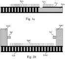
- Fig. 1a represents a first step of the manufacturing of a first part of a printed circuit board that is intended to embed a power die according to the present invention.
- the first part of the printed circuit board that is intended to embed a power die according to the present invention is composed of a printed circuit board Pcba that is composed of FR4 material and copper layers Cua.
- Nano wires Nwa are disposed on parts of the copper layer Cua.
- the nano wires are created on the copper pads of the first part of the printed circuit board.
- the nano wires are created on the power die itself.
- nano wires are formed by attaching/growing a porous alumina layer to the copper surface, copper electroplating, and selectively etching the layer.
- the formed nano wires are typically wires with length in the order of 10 ⁇ m and diameter in the order of 100nm.
- the ratio between length and diameter is typically higher than 10.
- the nano wires are sufficiently numerous, for example at least one million per cm 2 and may cover more than 50% of the treated surface to provide a high cumulative cross-section.
- the nano wires are processed in order to obtain consistent heights, thus facilitating a homogeneous contact with the surface of the power die. This can be done for example by a polishing step prior to porous layer etching.
- a step of surface coating may be added.
- a coating layer of non-bondable material may be deposited on the external surface of the nano wires by deposition techniques such as chemical vapor deposition, electroless of electrolytic deposition, or a combination of above mentioned techniques.
- Fig. 1b represents a first step of the manufacturing of a second part of a printed circuit board that is intended to embed a power die according to the present invention.
- the second part of the printed circuit board that is intended to embed a power die according to the present invention is composed of printed circuit boards Pcbb1 to Pcbb3 that are composed of FR4 material and the printed circuit boards Pcbb3 is further composed of copper layers Cub.
- Nano wires Nwb are disposed on parts of the copper layer Cub.
- the nano wires are created on the copper pads of the second part of the printed circuit board.
- the nano wires are created on the power die itself.
- nano wires are formed by attaching/growing a porous alumina layer to the copper surface, copper electroplating, and selectively etching the layer.
- the formed nano wires are typically wires with length in the order of 10 ⁇ m and diameter in the order of 100nm.
- the ratio between length and diameter is typically higher than 10.
- the nano wires are sufficiently numerous, for example at least one million per cm 2 and may cover more than 50% of the treated surface to provide a high cumulative cross-section.
- the nano wires are processed in order to obtain constant heights, thus facilitating a homogeneous contact with the surface of the power die. This can be done for example by a polishing step prior to porous layer etching.
- a step of surface coating may be added.
- a coating layer of non-bondable material may be deposited on the external surface of the nano wires by deposition techniques such as chemical vapor deposition, electroless of electrolytic deposition, or a combination of above mentioned techniques.
- the printed circuit board Pcbb1 comprises a spacer Sp1 that is intended to place the power die at a right position.
- the printed circuit board Pcbb2 comprises a spacer Sp2 that is intended to place the power die at the right position.
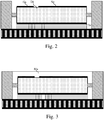
- Fig. 2 represents a second step of the manufacturing of the second part of a printed circuit board that is intended to embed a power die according to the present invention.
- the power die Di is placed in the cavity formed by the printed circuit boards Pcbb1 to Pcbb3. The location of the power die Di is determined by the spacers Sp1 and Sp2.
- the nano wires disposed on the copper layer Cub are in contact with the drain Dr of the power die Di.
- the drain Dr surface may be activated for example by adding a thin layer such as solder paste that may facilitate the contact and lead to a solid connection between the nano wires and the drain Dr surface.
- a thin layer such as solder paste
- solder paste may facilitate the contact and lead to a solid connection between the nano wires and the drain Dr surface.
- the use of a porous surface with small patterns, e.g. scratches or nano-cavities, or the generation of short, micrometer-range copper nano-wires may facilitate the connection between the nano wires and the surface of the drain Dr.
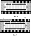
- Fig. 3 represents a third step of the manufacturing of the second part of a printed circuit board that is intended to embed a power die according to the present invention.
- the cavity formed by the printed circuit boards Pcbb1 to Pcbb3 is filled with a dielectric fluid in order to decrease the thermal resistance between die and case, thus facilitating the heat flow away from the power die Di, increase the thermal capacitance, thus limiting the temperature increase in case of surge current or short-circuits, prevent oxidation of the nano wires, prevent conglomeration of the wires together due to the joint action of heat and current and provide isolation between different electrical potentials such as gate-drain, source-drain or gate-source in the case of a MOSFET power die Di.
- the dielectric fluid may be liquid with various levels of viscosity like for example isolating silicone gel/grease, dielectric oil.
- the dielectric fluid has a low viscosity during cavity filling to allow the fluid to fill properly the volume of the cavity, especially between the nano wires. After the cavity filling, the viscosity may increase, for example to provide a gel-like viscosity.
- the fluid may also be a two-phase material like for example paraffin or other wax-like substance with a melting point chosen either sufficiently low like for example 42°C so that it is liquid during nominal operation, or higher like for example 200°C so that the dielectric fluid melts only during abnormal operation like surge currents or short-circuits.
- the transition energy is used to stabilize the temperature during surge currents and thus increases the robustness of the power die Di.
- the cavity may be filled during the assembly process as described previously, but alternatively, the cavity may be filled afterwards as it will be disclosed hereinafter.
- An additional step of mechanical agitation might be used before sealing in order to improve the fluid penetration withing the available space in the nano-wire forest.
- Fig. 4 represents the printed circuit board that embeds a power die according to the present invention.
- the printed circuit board is formed by the assembly of the first and second parts of the printed circuit board in order to form a press-pack type connection i.e. where the power die Di is sandwiched between two copper surfaces with the only effect of pressure.
- the pressure is first applied during a lamination process, but a residual pressure is present that holds the power die in position after the assembly process.
- Fig. 4 One example of process is described in Fig. 4 where the nano wires are created on a printed circuit board core with thermal vias. Previously milled prepreg layers are laminated to the core with previously created nano wires.
- Fig. 5 represents an example of a first variant of a printed circuit board that embeds a power die according to the present invention.
- the first part of the printed circuit board comprises two holes noted Ho1 and Ho2 that enable the filling of the cavity formed by the printed circuit boards Pcbb1 to Pcbb3 with the dielectric fluid after the assembly of the first and second parts of the printed circuit board.
- the holes Ho1 and Ho2 are filled up with a resin not shown in Fig. 5 .
- Fig. 6 represents an example of a second variant of a printed circuit board that embeds a power die according to the present invention.
- the first part of the printed circuit board comprises two membranes noted Me1 and Me2.
- Membranes act as expension valves.
- the membranes Me1 and Me2 are for example flexible membranes so that they can deform if the dielectric fluid expands or shrinks with temperature and/or phase change.
- Fig. 7 represents an example of a third variant of a printed circuit board that embeds a power die according to the present invention.
- the printed circuit boards Pcbb1 and Pcbb2 comprise cavities Ca1 and Ca2 that may be used to allow the dielectric fluid to expand and shrink in and out of the cavities Ca1 and Ca2.
- Fig. 8 represents an example of an algorithm for manufacturing a printed circuit board that embeds a power die according to the present invention.
- nano wires are created on parts of the copper layer Cua of the first part of the printed circuit board and on the copper layer Cub of the second part of the printed circuit board.
- the nano wires are created on the power die itself.
- nano wires are formed by attaching/growing a porous alumina layer to the copper surface, copper electroplating, and selectively etching the layer.
- the formed nano wires are typically wires with length in the order of 10 ⁇ m and diameter in the order of 100nm.
- the ratio between length and diameter is typically higher than 10.
- the nano wires are sufficiently numerous, for example at least one million per cm 2 and may cover more than 50% of the treated surface to provide a high cumulative cross-section.
- the nano wires are processed in order to obtain consistent heights, thus facilitating a homogeneous contact with the surface of the power die. This can be done for example by a polishing step prior to porous layer etching.
- a step of surface coating may be added.
- a coating layer of non-bondable material may be deposited on the external surface of the nano wires by deposition techniques such as chemical vapor deposition, electroless of electrolytic deposition, or a combination of the above mentioned techniques.
- the power die Di is placed in the cavity formed by the printed circuit boards Pcbb1 to Pcbb3 of the second part of the printed circuit board.
- the location of the power die Di is determined by the spacers Sp1 and Sp2.
- the nano wires disposed on the copper layer Cub are typically in contact with the drain Dr of the power die Di.
- the drain Dr surface may be activated for example by adding a thin layer such as solder paste that may facilitate the contact and lead to a solid connection between the nano wires and the drain Dr surface.
- a thin layer such as solder paste
- solder paste may facilitate the contact and lead to a solid connection between the nano wires and the drain Dr surface.
- the use of a porous surface with small patterns, e.g. scratches or nano-cavities, or the generation of short, micrometer-range copper nano-wires may facilitate the connection between the nano wires and the surface of the drain Dr.
- the cavity formed by the printed circuit boards Pcbb1 to Pcbb3 is filled with a dielectric fluid in order to decrease the thermal resistance between die and case, thus facilitating the heat flow away from the power die Di, increase the thermal capacitance, thus limiting the temperature increase in case of surge current or short-circuits, prevent oxidation of the nano wires, prevent conglomeration of the wires together due to the joint action of heat and current and provide isolation between different electrical potentials such as gate-drain, source-drain or gate-source in the case of a MOSFET power die Di.
- the dielectric fluid may be liquid with various levels of viscosity like for example isolating silicone gel/grease, dielectric oil.
- the dielectric fluid as a low viscosity during cavity filling to allow the fluid to fill properly the volume of the cavity, especially between the nano wires. After the cavity filling, the viscosity may increase, for example to provide a gel-like viscosity.
- the fluid may also be a two-phase material like for example paraffin or other wax-like substance with a melting point chosen either sufficiently low like for example 42°C so that it is liquid during nominal operation, or higher like for example 200°C, so that the dielectric fluid melts only during abnormal operation like surge currents or short-circuits.
- the transition energy is used to stabilize the temperature during surge currents and thus increases the robustness of the power die Di.
- the cavity may be filled during the assembly process as previously described, but alternatively, the cavity may be filled afterwards as it will be disclosed hereinafter.
- An additional step of mechanical agitation might be used before sealing in order to improve the fluid penetration withing the available space in the nano-wire forest.
- the printed circuit board is formed by the assembly of the first and second parts of the printed circuit board in order to form a press-pack type connection i.e. where the power die Di is sandwiched between two copper surfaces with the only effect of pressure.
- the pressure is first applied during a lamination process, but a residual pressure is present that holds the power die in position after the assembly process.
- step S83 maybe performed before the step S82.
- Fig. 9 represents an example of a fourth variant of a printed circuit board that embeds a power die according to the present invention.
- the printed circuit boards Pcbb1 and Pcbb2 comprise respectively flexible membranes FM1 and FM2 that deform when the fluid expands or shrinks with temperature and/or phase change of the fluid.
- the membranes FM1 and FM2 are for example flexible membranes so that they can deform if the dielectric fluid expands or shrinks with temperature and/or phase change.
- the membranes are typically composed of a flexible but impermeable material such as polyimide that is locally laminated in the printed circuit board assembly.
- the flexible membranes may also be located in the printed circuit boards Pcba and Pcbb3.
Landscapes
- Engineering & Computer Science (AREA)
- Microelectronics & Electronic Packaging (AREA)
- Manufacturing & Machinery (AREA)
- Metallurgy (AREA)
- Structure Of Printed Boards (AREA)
- Non-Metallic Protective Coatings For Printed Circuits (AREA)
- Cooling Or The Like Of Semiconductors Or Solid State Devices (AREA)
- Die Bonding (AREA)
- Chemical & Material Sciences (AREA)
- Dispersion Chemistry (AREA)
- Manufacturing Of Printed Wiring (AREA)
Abstract
Description
- The present invention relates generally to a printed circuit board embedding a power die and a method for manufacturing said printed circuit board embedding the power die.
- Power die embedding in Printed Circuit Boards (PCBs) is entering the market because it is a low-cost, low-inductance, low electro magnetic interference, and efficiently cooled technology compared to a more conventional power die assembly on a ceramic substrate. However, one remaining issue is the reliability of the interconnections between the power die and the copper pads of the printed circuit boards.
- Classically, the interconnections are either performed using soldering, sintering, direct copper deposition or using conductive adhesives.
- When the assembly is subject to thermo-mechanical stress like for example due to coefficient of thermal expansion mismatches and thermal gradient, the interconnection may be damaged, leading ultimately to the failure of the power module.
- Soft interconnection composed of micro/nano copper wires are proposed in order to overcome aforementioned problems. Nano wires have a high length compared to their diameter and are sufficiently flexible to deform at low strain and stress. They have relatively high density, forming a nano-wire forest, in order to effectively transfer current and heat.
- Thus, the mechanical displacements due to thermal effects between the die and the printed circuit board are absorbed by the nano wires without damaging them.
- However, nano wires may suffer adhesion/conglomeration/oxidation with the combined action of heat, current, and pressure.
- Such a conglomeration results in a hardening/welding of the nano-wire forrest and then the interconnection looses its flexibility.
- The present invention aims to allow a decrease of the thermal resistance between the power die and the printed circuit board, an increase of the thermal capacitance, prevent oxidation of the nano wires and prevent conglomeration of the nano wires together due to the joint action of heat and current.
- To that end, the present invention concerns a printed circuit board embedding a power die wherein interconnections between the power die and the printed circuit board are composed of micro/nano wires, the printed circuit board comprising a cavity wherein the power die is placed, characterized in that the cavity is further filled with a dielectric fluid.
- The present invention concerns also a method for manufacturing a printed circuit board embedding a power die wherein interconnections between the power die and the printed circuit board are composed of micro/nano wires, the printed circuit board comprising a cavity wherein the power die is placed, characterized in that the method comprises the step of filling the cavity with a dielectric fluid.
- Thus, the micro/nano wires are protected from adhesion, conglomeration, oxidation and isolation is enhanced between different electrical potentials such as gate-drain, source-drain or gate-source in the case of a MOSFET.
- According to a particular feature, the dielectric fluid is an isolating silicone gel or grease or a dielectric oil.
- Thus, the system can use low-cost and reliable dielectric fluids.
- According to a particular feature, the dielectric fluid has a low viscosity during cavity filling to allow the fluid to fill properly the volume of the cavity and between the nano wires.
- Thus, the entire remaining volume of the cavity is filled with the dielectric fluid, and the micro/nano wires are better protected from adhesion, conglomeration, oxidation and isolation is enhanced between different electrical potentials such as gate-drain, source-drain or gate-source in the case of a MOSFET.
- According to a particular feature, the dielectric fluid is a two-phase material.
- Thus, the transition energy is used to stabilize the temperature during surge currents and thus increases the robustness of the device.
- According to a particular feature, the printed circuit board further comprises at least one other cavity for enabling the dielectric fluid to shrink in and out of the at least one other cavity.
- Thus, the pressure variations in the first cavity can be reduced.
- According to a particular feature, the printed circuit board further comprises holes that enable the filling of the dielectric fluid within the cavity and the holes are filled up with a resin after the filling of the dielectric fluid within the cavity.
- Thus, the filling of the cavity is realized after the assembly of the printed circuit board embedding a power die and more standard processes can be used.
- According to a particular feature, the printed circuit board further comprises flexible membranes that deform when the fluid expands or shrinks with temperature and/or phase change of the fluid.
- Thus the pressure variations in the first cavity can be reduced.
- According to a particular feature, the printed circuit board further comprises holes that enable the filling of the dielectric fluid within the cavity and the holes are closed with flexible membranes after the filling of the dielectric fluid within the cavity.
- Thus, the membranes also serve as holes and the fabrication process is simplified.
- The characteristics of the invention will emerge more clearly from a reading of the following description of example embodiments, the said description being produced with reference to the accompanying drawings, among which:
-
Figs. 1 to 4 represent the different steps of a manufacturing of a printed circuit board that embeds a power die according to the present invention; -
Fig. 5 represents an example of a first variant of a printed circuit board that embeds a power die according to the present invention; -
Fig. 6 represents an example of a second variant of a printed circuit board that embeds a power die according to the present invention; -
Fig. 7 represents an example of a third variant of a printed circuit board that embeds a power die according to the present invention; -
Fig. 8 represents an example of an algorithm for manufacturing a printed circuit board that embeds a power die according to the present invention; -
Fig. 9 represents an example of a fourth variant of a printed circuit board that embeds a power die according to the present invention. -
Fig. 1a represents a first step of the manufacturing of a first part of a printed circuit board that is intended to embed a power die according to the present invention. - The first part of the printed circuit board that is intended to embed a power die according to the present invention is composed of a printed circuit board Pcba that is composed of FR4 material and copper layers Cua.
- Nano wires Nwa are disposed on parts of the copper layer Cua.
- In the example of
Fig. 1a , the nano wires are created on the copper pads of the first part of the printed circuit board. - Alternatively, the nano wires are created on the power die itself.
- For example, nano wires are formed by attaching/growing a porous alumina layer to the copper surface, copper electroplating, and selectively etching the layer.
- The formed nano wires are typically wires with length in the order of 10µm and diameter in the order of 100nm. The ratio between length and diameter is typically higher than 10. The nano wires are sufficiently numerous, for example at least one million per cm2 and may cover more than 50% of the treated surface to provide a high cumulative cross-section. The nano wires are processed in order to obtain consistent heights, thus facilitating a homogeneous contact with the surface of the power die. This can be done for example by a polishing step prior to porous layer etching.
- In order to prevent adhesion of the wires together due to the joint action of heat and current, a step of surface coating may be added.
- For example, a coating layer of non-bondable material may be deposited on the external surface of the nano wires by deposition techniques such as chemical vapor deposition, electroless of electrolytic deposition, or a combination of above mentioned techniques.
-
Fig. 1b represents a first step of the manufacturing of a second part of a printed circuit board that is intended to embed a power die according to the present invention. - The second part of the printed circuit board that is intended to embed a power die according to the present invention is composed of printed circuit boards Pcbb1 to Pcbb3 that are composed of FR4 material and the printed circuit boards Pcbb3 is further composed of copper layers Cub.
- Nano wires Nwb are disposed on parts of the copper layer Cub.
- In the example of
Fig. 1b , the nano wires are created on the copper pads of the second part of the printed circuit board. - Alternatively, the nano wires are created on the power die itself.
- For example, nano wires are formed by attaching/growing a porous alumina layer to the copper surface, copper electroplating, and selectively etching the layer.
- The formed nano wires are typically wires with length in the order of 10µm and diameter in the order of 100nm. The ratio between length and diameter is typically higher than 10. The nano wires are sufficiently numerous, for example at least one million per cm2 and may cover more than 50% of the treated surface to provide a high cumulative cross-section. The nano wires are processed in order to obtain constant heights, thus facilitating a homogeneous contact with the surface of the power die. This can be done for example by a polishing step prior to porous layer etching.
- In order to prevent adhesion of the nano wires together due to the joint action of heat and current, a step of surface coating may be added.
- For example, a coating layer of non-bondable material may be deposited on the external surface of the nano wires by deposition techniques such as chemical vapor deposition, electroless of electrolytic deposition, or a combination of above mentioned techniques.
- The printed circuit board Pcbb1 comprises a spacer Sp1 that is intended to place the power die at a right position.
- The printed circuit board Pcbb2 comprises a spacer Sp2 that is intended to place the power die at the right position.
-
Fig. 2 represents a second step of the manufacturing of the second part of a printed circuit board that is intended to embed a power die according to the present invention. - Once the second part of the printed circuit board is manufactured, the power die Di is placed in the cavity formed by the printed circuit boards Pcbb1 to Pcbb3. The location of the power die Di is determined by the spacers Sp1 and Sp2.
- The nano wires disposed on the copper layer Cub are in contact with the drain Dr of the power die Di.
- In order to allow a high electrical and thermal conductivity and to prevent flattening of the nano wires during the assembly, the drain Dr surface may be activated for example by adding a thin layer such as solder paste that may facilitate the contact and lead to a solid connection between the nano wires and the drain Dr surface. The use of a porous surface with small patterns, e.g. scratches or nano-cavities, or the generation of short, micrometer-range copper nano-wires may facilitate the connection between the nano wires and the surface of the drain Dr.
-
Fig. 3 represents a third step of the manufacturing of the second part of a printed circuit board that is intended to embed a power die according to the present invention. - In the third step, the cavity formed by the printed circuit boards Pcbb1 to Pcbb3 is filled with a dielectric fluid in order to decrease the thermal resistance between die and case, thus facilitating the heat flow away from the power die Di, increase the thermal capacitance, thus limiting the temperature increase in case of surge current or short-circuits, prevent oxidation of the nano wires, prevent conglomeration of the wires together due to the joint action of heat and current and provide isolation between different electrical potentials such as gate-drain, source-drain or gate-source in the case of a MOSFET power die Di.
- The dielectric fluid may be liquid with various levels of viscosity like for example isolating silicone gel/grease, dielectric oil. The dielectric fluid has a low viscosity during cavity filling to allow the fluid to fill properly the volume of the cavity, especially between the nano wires. After the cavity filling, the viscosity may increase, for example to provide a gel-like viscosity. The fluid may also be a two-phase material like for example paraffin or other wax-like substance with a melting point chosen either sufficiently low like for example 42°C so that it is liquid during nominal operation, or higher like for example 200°C so that the dielectric fluid melts only during abnormal operation like surge currents or short-circuits. Thus, the transition energy is used to stabilize the temperature during surge currents and thus increases the robustness of the power die Di.
- The cavity may be filled during the assembly process as described previously, but alternatively, the cavity may be filled afterwards as it will be disclosed hereinafter.
- An additional step of mechanical agitation, for example using ultrasoind bath, might be used before sealing in order to improve the fluid penetration withing the available space in the nano-wire forest.
-
Fig. 4 represents the printed circuit board that embeds a power die according to the present invention. - The printed circuit board is formed by the assembly of the first and second parts of the printed circuit board in order to form a press-pack type connection i.e. where the power die Di is sandwiched between two copper surfaces with the only effect of pressure. The pressure is first applied during a lamination process, but a residual pressure is present that holds the power die in position after the assembly process.
- One example of process is described in
Fig. 4 where the nano wires are created on a printed circuit board core with thermal vias. Previously milled prepreg layers are laminated to the core with previously created nano wires. -
Fig. 5 represents an example of a first variant of a printed circuit board that embeds a power die according to the present invention. - In the example of
Fig. 5 , the first part of the printed circuit board comprises two holes noted Ho1 and Ho2 that enable the filling of the cavity formed by the printed circuit boards Pcbb1 to Pcbb3 with the dielectric fluid after the assembly of the first and second parts of the printed circuit board. - Once the cavity formed by the printed circuit boards Pcbb1 to Pcbb3 is filled with the dielectric fluid, the holes Ho1 and Ho2 are filled up with a resin not shown in
Fig. 5 . -
Fig. 6 represents an example of a second variant of a printed circuit board that embeds a power die according to the present invention. - In the example of
Fig. 6 , the first part of the printed circuit board comprises two membranes noted Me1 and Me2. Membranes act as expension valves. The membranes Me1 and Me2 are for example flexible membranes so that they can deform if the dielectric fluid expands or shrinks with temperature and/or phase change. -
Fig. 7 represents an example of a third variant of a printed circuit board that embeds a power die according to the present invention. - In the example of
Fig. 7 , the printed circuit boards Pcbb1 and Pcbb2 comprise cavities Ca1 and Ca2 that may be used to allow the dielectric fluid to expand and shrink in and out of the cavities Ca1 and Ca2. -
Fig. 8 represents an example of an algorithm for manufacturing a printed circuit board that embeds a power die according to the present invention. - At step S80, nano wires are created on parts of the copper layer Cua of the first part of the printed circuit board and on the copper layer Cub of the second part of the printed circuit board.
- Alternatively, the nano wires are created on the power die itself.
- For example, nano wires are formed by attaching/growing a porous alumina layer to the copper surface, copper electroplating, and selectively etching the layer.
- The formed nano wires are typically wires with length in the order of 10µm and diameter in the order of 100nm. The ratio between length and diameter is typically higher than 10. The nano wires are sufficiently numerous, for example at least one million per cm2 and may cover more than 50% of the treated surface to provide a high cumulative cross-section. The nano wires are processed in order to obtain consistent heights, thus facilitating a homogeneous contact with the surface of the power die. This can be done for example by a polishing step prior to porous layer etching.
- In order to prevent adhesion of the wires together due to the joint action of heat and current, a step of surface coating may be added.
- For example, a coating layer of non-bondable material may be deposited on the external surface of the nano wires by deposition techniques such as chemical vapor deposition, electroless of electrolytic deposition, or a combination of the above mentioned techniques.
- At step S81, the power die Di is placed in the cavity formed by the printed circuit boards Pcbb1 to Pcbb3 of the second part of the printed circuit board. The location of the power die Di is determined by the spacers Sp1 and Sp2.
- The nano wires disposed on the copper layer Cub are typically in contact with the drain Dr of the power die Di.
- In order to allow a high electrical and thermal conductivity and to prevent flattening of the nano wires during the assembly, the drain Dr surface may be activated for example by adding a thin layer such as solder paste that may facilitate the contact and lead to a solid connection between the nano wires and the drain Dr surface. The use of a porous surface with small patterns, e.g. scratches or nano-cavities, or the generation of short, micrometer-range copper nano-wires may facilitate the connection between the nano wires and the surface of the drain Dr.
- At step S82, the cavity formed by the printed circuit boards Pcbb1 to Pcbb3 is filled with a dielectric fluid in order to decrease the thermal resistance between die and case, thus facilitating the heat flow away from the power die Di, increase the thermal capacitance, thus limiting the temperature increase in case of surge current or short-circuits, prevent oxidation of the nano wires, prevent conglomeration of the wires together due to the joint action of heat and current and provide isolation between different electrical potentials such as gate-drain, source-drain or gate-source in the case of a MOSFET power die Di.
- The dielectric fluid may be liquid with various levels of viscosity like for example isolating silicone gel/grease, dielectric oil. The dielectric fluid as a low viscosity during cavity filling to allow the fluid to fill properly the volume of the cavity, especially between the nano wires. After the cavity filling, the viscosity may increase, for example to provide a gel-like viscosity. The fluid may also be a two-phase material like for example paraffin or other wax-like substance with a melting point chosen either sufficiently low like for example 42°C so that it is liquid during nominal operation, or higher like for example 200°C, so that the dielectric fluid melts only during abnormal operation like surge currents or short-circuits. Thus, the transition energy is used to stabilize the temperature during surge currents and thus increases the robustness of the power die Di.
- The cavity may be filled during the assembly process as previously described, but alternatively, the cavity may be filled afterwards as it will be disclosed hereinafter.
- An additional step of mechanical agitation, for example using ultrasoind bath, might be used before sealing in order to improve the fluid penetration withing the available space in the nano-wire forest.
- At next step S83, the printed circuit board is formed by the assembly of the first and second parts of the printed circuit board in order to form a press-pack type connection i.e. where the power die Di is sandwiched between two copper surfaces with the only effect of pressure. The pressure is first applied during a lamination process, but a residual pressure is present that holds the power die in position after the assembly process.
- It has to be noted here, as diclosed in reference to
Figs. 5 or6 or 7 , that the step S83 maybe performed before the step S82. -
Fig. 9 represents an example of a fourth variant of a printed circuit board that embeds a power die according to the present invention. - In the fourth variant, the printed circuit boards Pcbb1 and Pcbb2 comprise respectively flexible membranes FM1 and FM2 that deform when the fluid expands or shrinks with temperature and/or phase change of the fluid.
- The membranes FM1 and FM2 are for example flexible membranes so that they can deform if the dielectric fluid expands or shrinks with temperature and/or phase change. The membranes are typically composed of a flexible but impermeable material such as polyimide that is locally laminated in the printed circuit board assembly.
- It has to be noted here that the flexible membranes may also be located in the printed circuit boards Pcba and Pcbb3.
- Naturally, many modifications can be made to the embodiments of the invention described above without departing from the scope of the present invention.
Claims (9)
- A printed circuit board embedding a power die wherein interconnections between the power die and the printed circuit board are composed of micro/nano wires, the printed circuit board comprising a cavity wherein the power die is placed, characterized in that the cavity is further filled with a dielectric fluid.
- The printed circuit board according to claim 1, characterized in that the dielectric fluid is an isolating silicone gel or grease or a dielectric oil.
- The printed circuit board according to claim 2, characterized in that the dielectric fluid has a low viscosity during cavity filling to allow the fluid to fill properly the volume of the cavity and between the nano wires.
- The printed circuit board according to claim 1, characterized in that the dielectric fluid is a two-phase material.
- The printed circuit board according to any of the claims 1 to 4, characterized in that the printed circuit board further comprises at least one other cavity for enabling the dielectric fluid to shrink in and out of the at least one other cavity.
- The printed circuit board according to any of the claims 1 to 5, characterized in that the printed circuit board further comprises holes that enable the filling of the dielectric fluid within the cavity and the holes are filled up with a resin after the filling of the dielectric fluid within the cavity.
- The printed circuit board according to any of the claims 1 to 5, characterized in that the printed circuit board further comprises flexible membranes that deform when the fluid expands or shrinks with temperature and/or phase change of the fluid.
- The printed circuit board according to any of the claims 1 to 5, characterized in that the printed circuit board further comprises holes that enable the filling of the dielectric fluid within the cavity and the holes are closed with flexible membranes after the filling of the dielectric fluid within the cavity.
- A method for manufacturing a printed circuit board embedding a power die wherein interconnections between the power die and the printed circuit board are composed of micro/nano wires, the printed circuit board comprising a cavity wherein the power die is placed, characterized in that the method comprises the step of filling the cavity with a dielectric fluid.
Priority Applications (5)
| Application Number | Priority Date | Filing Date | Title |
|---|---|---|---|
| EP17151014.2A EP3349551B1 (en) | 2017-01-11 | 2017-01-11 | A printed circuit board embedding a power die and a method for manufacturing said printed circuit board |
| PCT/JP2017/044802 WO2018131374A1 (en) | 2017-01-11 | 2017-12-07 | Printed circuit board and method for manufacturing printed circuit board |
| JP2019509579A JP6749475B2 (en) | 2017-01-11 | 2017-12-07 | Printed circuit board and method for making printed circuit board |
| US16/461,896 US10827619B2 (en) | 2017-01-11 | 2017-12-07 | Printed circuit board and method for manufacturing printed circuit board |
| CN201780079100.XA CN110140432B (en) | 2017-01-11 | 2017-12-07 | Printed circuit board and method for manufacturing printed circuit board |
Applications Claiming Priority (1)
| Application Number | Priority Date | Filing Date | Title |
|---|---|---|---|
| EP17151014.2A EP3349551B1 (en) | 2017-01-11 | 2017-01-11 | A printed circuit board embedding a power die and a method for manufacturing said printed circuit board |
Publications (2)
| Publication Number | Publication Date |
|---|---|
| EP3349551A1 true EP3349551A1 (en) | 2018-07-18 |
| EP3349551B1 EP3349551B1 (en) | 2024-12-18 |
Family
ID=57796183
Family Applications (1)
| Application Number | Title | Priority Date | Filing Date |
|---|---|---|---|
| EP17151014.2A Active EP3349551B1 (en) | 2017-01-11 | 2017-01-11 | A printed circuit board embedding a power die and a method for manufacturing said printed circuit board |
Country Status (5)
| Country | Link |
|---|---|
| US (1) | US10827619B2 (en) |
| EP (1) | EP3349551B1 (en) |
| JP (1) | JP6749475B2 (en) |
| CN (1) | CN110140432B (en) |
| WO (1) | WO2018131374A1 (en) |
Cited By (1)
| Publication number | Priority date | Publication date | Assignee | Title |
|---|---|---|---|---|
| US12218018B2 (en) | 2022-04-21 | 2025-02-04 | Infineon Technologies Ag | Semiconductor encapsulant strength enhancer |
Families Citing this family (12)
| Publication number | Priority date | Publication date | Assignee | Title |
|---|---|---|---|---|
| MY201466A (en) * | 2017-10-26 | 2024-02-24 | Syed Taymur Ahmad | Composition comprising non-newtonian fluids for hydrophobic, oleophobic, and oleophilic coatings, and methods of using the same |
| CN112243314A (en) * | 2019-07-18 | 2021-01-19 | 华为技术有限公司 | Circuit board assembly, manufacturing method of circuit board assembly and electronic equipment |
| JP7499869B2 (en) * | 2020-03-18 | 2024-06-14 | ナノワイヤード ゲーエムベーハー | Connecting the parts |
| DE102021112814A1 (en) | 2021-05-18 | 2022-11-24 | Unimicron Germany GmbH | Process for manufacturing a printed circuit board and printed circuit board with at least one embedded electronic component |
| DE102021209486A1 (en) * | 2021-08-30 | 2023-03-02 | Robert Bosch Gesellschaft mit beschränkter Haftung | Electronic arrangement and method for its production |
| CN113593841B (en) * | 2021-09-28 | 2021-12-07 | 广东力王高新科技股份有限公司 | High-power planar transformer and electronic equipment |
| EP4255131A1 (en) | 2022-03-31 | 2023-10-04 | AT & S Austria Technologie & Systemtechnik Aktiengesellschaft | Component carrier and method for producing a component carrier |
| KR20230157086A (en) * | 2022-05-09 | 2023-11-16 | 현대자동차주식회사 | Direct cooling type power module |
| EP4345866A1 (en) * | 2022-09-27 | 2024-04-03 | Mitsubishi Electric R & D Centre Europe B.V. | A method and a system for manufacturing an assembly of a power semiconductor |
| EP4372799A1 (en) * | 2022-11-15 | 2024-05-22 | NanoWired GmbH | Bonding a semiconductor element to a substrate |
| CN116093035A (en) * | 2023-02-10 | 2023-05-09 | 珠海越亚半导体股份有限公司 | Packaging carrier plate embedded with efficient heat dissipation module and manufacturing method thereof |
| CN116759388B (en) * | 2023-08-18 | 2023-10-27 | 合肥阿基米德电子科技有限公司 | Welding-free module packaging structure |
Citations (3)
| Publication number | Priority date | Publication date | Assignee | Title |
|---|---|---|---|---|
| US20030015778A1 (en) * | 2001-07-23 | 2003-01-23 | Shin Soyano | Semiconductor device |
| US20100013085A1 (en) * | 2008-07-18 | 2010-01-21 | Mitsubishi Electric Corporation | Power semiconductor device |
| EP2871675A1 (en) * | 2013-11-06 | 2015-05-13 | Mitsubishi Electric R & D Centre Europe B.V. | Pressure connection for a semiconductor die using flexible nanowires and corresponding manufacturing method |
Family Cites Families (9)
| Publication number | Priority date | Publication date | Assignee | Title |
|---|---|---|---|---|
| JP2001244386A (en) * | 2000-02-28 | 2001-09-07 | Hitachi Ltd | Power semiconductor module |
| JP3624840B2 (en) * | 2000-05-16 | 2005-03-02 | Fdk株式会社 | Inductor |
| DE10127351A1 (en) * | 2001-06-06 | 2002-12-19 | Infineon Technologies Ag | Electronic chip comprises several external contacts of which at least two are provided with a plurality of nano-tubes for purposes of contacting an external contact of another electronic chip |
| JP2003068979A (en) * | 2001-08-28 | 2003-03-07 | Hitachi Ltd | Semiconductor device |
| JP4744360B2 (en) * | 2006-05-22 | 2011-08-10 | 富士通株式会社 | Semiconductor device |
| JP5245925B2 (en) * | 2009-03-06 | 2013-07-24 | 富士通株式会社 | Electronic component and manufacturing method thereof |
| EP2546871B1 (en) * | 2010-03-12 | 2018-12-05 | Fujitsu Limited | Method for producing a heat dissipating structure |
| US8543190B2 (en) * | 2010-07-30 | 2013-09-24 | Medtronic, Inc. | Inductive coil device on flexible substrate |
| JP2015216199A (en) * | 2014-05-09 | 2015-12-03 | 新光電気工業株式会社 | Semiconductor device, heat conduction member, and method for manufacturing semiconductor device |
-
2017
- 2017-01-11 EP EP17151014.2A patent/EP3349551B1/en active Active
- 2017-12-07 US US16/461,896 patent/US10827619B2/en active Active
- 2017-12-07 WO PCT/JP2017/044802 patent/WO2018131374A1/en not_active Ceased
- 2017-12-07 CN CN201780079100.XA patent/CN110140432B/en active Active
- 2017-12-07 JP JP2019509579A patent/JP6749475B2/en active Active
Patent Citations (3)
| Publication number | Priority date | Publication date | Assignee | Title |
|---|---|---|---|---|
| US20030015778A1 (en) * | 2001-07-23 | 2003-01-23 | Shin Soyano | Semiconductor device |
| US20100013085A1 (en) * | 2008-07-18 | 2010-01-21 | Mitsubishi Electric Corporation | Power semiconductor device |
| EP2871675A1 (en) * | 2013-11-06 | 2015-05-13 | Mitsubishi Electric R & D Centre Europe B.V. | Pressure connection for a semiconductor die using flexible nanowires and corresponding manufacturing method |
Cited By (1)
| Publication number | Priority date | Publication date | Assignee | Title |
|---|---|---|---|---|
| US12218018B2 (en) | 2022-04-21 | 2025-02-04 | Infineon Technologies Ag | Semiconductor encapsulant strength enhancer |
Also Published As
| Publication number | Publication date |
|---|---|
| JP2019532492A (en) | 2019-11-07 |
| CN110140432B (en) | 2022-02-25 |
| JP6749475B2 (en) | 2020-09-02 |
| US10827619B2 (en) | 2020-11-03 |
| WO2018131374A1 (en) | 2018-07-19 |
| CN110140432A (en) | 2019-08-16 |
| EP3349551B1 (en) | 2024-12-18 |
| US20190320534A1 (en) | 2019-10-17 |
Similar Documents
| Publication | Publication Date | Title |
|---|---|---|
| EP3349551B1 (en) | A printed circuit board embedding a power die and a method for manufacturing said printed circuit board | |
| CN105164798B (en) | The method of electronic building brick and manufacture electronic building brick | |
| US20160324004A1 (en) | Method for Embedding a Component in a Printed Circuit Board | |
| CN103021982B (en) | Integrated circuit and manufacturing method | |
| KR20150104033A (en) | Ultra-thin embedded semiconductor device package and method of manufacturing therof | |
| JP2007535156A (en) | Heat conduction from embedded components. | |
| US11744004B2 (en) | Circuit board and method of manufacturing the same | |
| JP4494785B2 (en) | Anisotropic conductive adhesive film, method for producing the same, and semiconductor device | |
| US20140041906A1 (en) | Metal heat radiation substrate and manufacturing method thereof | |
| EP3216325A1 (en) | Circuit board with integrated prefabricated heat pipe and reinforced heat pipe | |
| CN105517344A (en) | Embedded board and method of manufacturing the same | |
| CN116456619B (en) | Manufacturing method of printed circuit board | |
| US20170135196A1 (en) | Heat dissipation member and printed circuit board having the same | |
| CN103460819A (en) | Wiring substrate | |
| CN106465546A (en) | Method for producing a printed circuit board with an embedded sensor chip, and printed circuit board | |
| EP3340753B1 (en) | Method of integrating a connector member with component carrier | |
| JP4903320B2 (en) | Manufacturing method of wiring board with electronic element | |
| JP2004179647A (en) | Wiring board, semiconductor package, base insulating film, and method of manufacturing wiring board | |
| JP2008130722A (en) | Circuit board with built-in solid electrolytic capacitor and manufacturing method thereof | |
| TWI736421B (en) | Circuitboard and manufacture method thereof | |
| JP7214008B2 (en) | Electrical power assemblies with thick conductive layers | |
| JP5836751B2 (en) | Thin film wiring board | |
| KR102141102B1 (en) | Method for manufacturing semiconductor package substrate and semiconductor package substrate manufactured using the same | |
| US20150319863A1 (en) | Structure and method for preparing a housing to accept a component for an embedded component printed circuit board | |
| JP2014220305A (en) | Multilayer substrate and electronic device using the same, method of manufacturing electronic device |
Legal Events
| Date | Code | Title | Description |
|---|---|---|---|
| PUAI | Public reference made under article 153(3) epc to a published international application that has entered the european phase |
Free format text: ORIGINAL CODE: 0009012 |
|
| STAA | Information on the status of an ep patent application or granted ep patent |
Free format text: STATUS: THE APPLICATION HAS BEEN PUBLISHED |
|
| AK | Designated contracting states |
Kind code of ref document: A1 Designated state(s): AL AT BE BG CH CY CZ DE DK EE ES FI FR GB GR HR HU IE IS IT LI LT LU LV MC MK MT NL NO PL PT RO RS SE SI SK SM TR |
|
| AX | Request for extension of the european patent |
Extension state: BA ME |
|
| STAA | Information on the status of an ep patent application or granted ep patent |
Free format text: STATUS: REQUEST FOR EXAMINATION WAS MADE |
|
| 17P | Request for examination filed |
Effective date: 20190110 |
|
| RBV | Designated contracting states (corrected) |
Designated state(s): AL AT BE BG CH CY CZ DE DK EE ES FI FR GB GR HR HU IE IS IT LI LT LU LV MC MK MT NL NO PL PT RO RS SE SI SK SM TR |
|
| STAA | Information on the status of an ep patent application or granted ep patent |
Free format text: STATUS: EXAMINATION IS IN PROGRESS |
|
| 17Q | First examination report despatched |
Effective date: 20210621 |
|
| GRAP | Despatch of communication of intention to grant a patent |
Free format text: ORIGINAL CODE: EPIDOSNIGR1 |
|
| STAA | Information on the status of an ep patent application or granted ep patent |
Free format text: STATUS: GRANT OF PATENT IS INTENDED |
|
| RIC1 | Information provided on ipc code assigned before grant |
Ipc: H05K 3/36 20060101ALN20240621BHEP Ipc: H05K 3/32 20060101ALN20240621BHEP Ipc: H05K 1/14 20060101ALN20240621BHEP Ipc: H05K 1/02 20060101ALN20240621BHEP Ipc: H01L 23/498 20060101ALN20240621BHEP Ipc: H01L 23/055 20060101ALN20240621BHEP Ipc: H05K 3/46 20060101ALN20240621BHEP Ipc: H01L 23/00 20060101ALI20240621BHEP Ipc: H01L 23/48 20060101ALI20240621BHEP Ipc: H01L 23/24 20060101ALI20240621BHEP Ipc: H01L 23/22 20060101ALI20240621BHEP Ipc: H01L 25/00 20060101ALI20240621BHEP Ipc: H05K 1/18 20060101AFI20240621BHEP |
|
| RIC1 | Information provided on ipc code assigned before grant |
Ipc: H05K 3/36 20060101ALN20240703BHEP Ipc: H05K 3/32 20060101ALN20240703BHEP Ipc: H05K 1/14 20060101ALN20240703BHEP Ipc: H05K 1/02 20060101ALN20240703BHEP Ipc: H01L 23/498 20060101ALN20240703BHEP Ipc: H01L 23/055 20060101ALN20240703BHEP Ipc: H05K 3/46 20060101ALN20240703BHEP Ipc: H01L 23/00 20060101ALI20240703BHEP Ipc: H01L 23/48 20060101ALI20240703BHEP Ipc: H01L 23/24 20060101ALI20240703BHEP Ipc: H01L 23/22 20060101ALI20240703BHEP Ipc: H01L 25/00 20060101ALI20240703BHEP Ipc: H05K 1/18 20060101AFI20240703BHEP |
|
| RIC1 | Information provided on ipc code assigned before grant |
Ipc: H05K 3/36 20060101ALN20240709BHEP Ipc: H05K 3/32 20060101ALN20240709BHEP Ipc: H05K 1/14 20060101ALN20240709BHEP Ipc: H05K 1/02 20060101ALN20240709BHEP Ipc: H01L 23/498 20060101ALN20240709BHEP Ipc: H01L 23/055 20060101ALN20240709BHEP Ipc: H05K 3/46 20060101ALN20240709BHEP Ipc: H01L 23/00 20060101ALI20240709BHEP Ipc: H01L 23/48 20060101ALI20240709BHEP Ipc: H01L 23/24 20060101ALI20240709BHEP Ipc: H01L 23/22 20060101ALI20240709BHEP Ipc: H01L 25/00 20060101ALI20240709BHEP Ipc: H05K 1/18 20060101AFI20240709BHEP |
|
| INTG | Intention to grant announced |
Effective date: 20240726 |
|
| RIC1 | Information provided on ipc code assigned before grant |
Ipc: H05K 3/36 20060101ALN20240717BHEP Ipc: H05K 3/32 20060101ALN20240717BHEP Ipc: H05K 1/14 20060101ALN20240717BHEP Ipc: H05K 1/02 20060101ALN20240717BHEP Ipc: H01L 23/498 20060101ALN20240717BHEP Ipc: H01L 23/055 20060101ALN20240717BHEP Ipc: H05K 3/46 20060101ALN20240717BHEP Ipc: H01L 23/00 20060101ALI20240717BHEP Ipc: H01L 23/48 20060101ALI20240717BHEP Ipc: H01L 23/24 20060101ALI20240717BHEP Ipc: H01L 23/22 20060101ALI20240717BHEP Ipc: H01L 25/00 20060101ALI20240717BHEP Ipc: H05K 1/18 20060101AFI20240717BHEP |
|
| GRAS | Grant fee paid |
Free format text: ORIGINAL CODE: EPIDOSNIGR3 |
|
| GRAA | (expected) grant |
Free format text: ORIGINAL CODE: 0009210 |
|
| STAA | Information on the status of an ep patent application or granted ep patent |
Free format text: STATUS: THE PATENT HAS BEEN GRANTED |
|
| AK | Designated contracting states |
Kind code of ref document: B1 Designated state(s): AL AT BE BG CH CY CZ DE DK EE ES FI FR GB GR HR HU IE IS IT LI LT LU LV MC MK MT NL NO PL PT RO RS SE SI SK SM TR |
|
| REG | Reference to a national code |
Ref country code: GB Ref legal event code: FG4D |
|
| REG | Reference to a national code |
Ref country code: CH Ref legal event code: EP |
|
| REG | Reference to a national code |
Ref country code: DE Ref legal event code: R096 Ref document number: 602017086803 Country of ref document: DE |
|
| REG | Reference to a national code |
Ref country code: IE Ref legal event code: FG4D |
|
| REG | Reference to a national code |
Ref country code: LT Ref legal event code: MG9D |
|
| PG25 | Lapsed in a contracting state [announced via postgrant information from national office to epo] |
Ref country code: HR Free format text: LAPSE BECAUSE OF FAILURE TO SUBMIT A TRANSLATION OF THE DESCRIPTION OR TO PAY THE FEE WITHIN THE PRESCRIBED TIME-LIMIT Effective date: 20241218 |
|
| PG25 | Lapsed in a contracting state [announced via postgrant information from national office to epo] |
Ref country code: FI Free format text: LAPSE BECAUSE OF FAILURE TO SUBMIT A TRANSLATION OF THE DESCRIPTION OR TO PAY THE FEE WITHIN THE PRESCRIBED TIME-LIMIT Effective date: 20241218 |
|
| PG25 | Lapsed in a contracting state [announced via postgrant information from national office to epo] |
Ref country code: BG Free format text: LAPSE BECAUSE OF FAILURE TO SUBMIT A TRANSLATION OF THE DESCRIPTION OR TO PAY THE FEE WITHIN THE PRESCRIBED TIME-LIMIT Effective date: 20241218 |
|
| PG25 | Lapsed in a contracting state [announced via postgrant information from national office to epo] |
Ref country code: NO Free format text: LAPSE BECAUSE OF FAILURE TO SUBMIT A TRANSLATION OF THE DESCRIPTION OR TO PAY THE FEE WITHIN THE PRESCRIBED TIME-LIMIT Effective date: 20250318 |
|
| REG | Reference to a national code |
Ref country code: NL Ref legal event code: MP Effective date: 20241218 |
|
| PG25 | Lapsed in a contracting state [announced via postgrant information from national office to epo] |
Ref country code: GR Free format text: LAPSE BECAUSE OF FAILURE TO SUBMIT A TRANSLATION OF THE DESCRIPTION OR TO PAY THE FEE WITHIN THE PRESCRIBED TIME-LIMIT Effective date: 20250319 Ref country code: LV Free format text: LAPSE BECAUSE OF FAILURE TO SUBMIT A TRANSLATION OF THE DESCRIPTION OR TO PAY THE FEE WITHIN THE PRESCRIBED TIME-LIMIT Effective date: 20241218 |
|
| PG25 | Lapsed in a contracting state [announced via postgrant information from national office to epo] |
Ref country code: RS Free format text: LAPSE BECAUSE OF FAILURE TO SUBMIT A TRANSLATION OF THE DESCRIPTION OR TO PAY THE FEE WITHIN THE PRESCRIBED TIME-LIMIT Effective date: 20250318 |
|
| PG25 | Lapsed in a contracting state [announced via postgrant information from national office to epo] |
Ref country code: NL Free format text: LAPSE BECAUSE OF FAILURE TO SUBMIT A TRANSLATION OF THE DESCRIPTION OR TO PAY THE FEE WITHIN THE PRESCRIBED TIME-LIMIT Effective date: 20241218 |
|
| REG | Reference to a national code |
Ref country code: AT Ref legal event code: MK05 Ref document number: 1753319 Country of ref document: AT Kind code of ref document: T Effective date: 20241218 |
|
| PG25 | Lapsed in a contracting state [announced via postgrant information from national office to epo] |
Ref country code: SM Free format text: LAPSE BECAUSE OF FAILURE TO SUBMIT A TRANSLATION OF THE DESCRIPTION OR TO PAY THE FEE WITHIN THE PRESCRIBED TIME-LIMIT Effective date: 20241218 |
|
| PG25 | Lapsed in a contracting state [announced via postgrant information from national office to epo] |
Ref country code: PL Free format text: LAPSE BECAUSE OF FAILURE TO SUBMIT A TRANSLATION OF THE DESCRIPTION OR TO PAY THE FEE WITHIN THE PRESCRIBED TIME-LIMIT Effective date: 20241218 |
|
| PG25 | Lapsed in a contracting state [announced via postgrant information from national office to epo] |
Ref country code: ES Free format text: LAPSE BECAUSE OF FAILURE TO SUBMIT A TRANSLATION OF THE DESCRIPTION OR TO PAY THE FEE WITHIN THE PRESCRIBED TIME-LIMIT Effective date: 20241218 |
|
| PG25 | Lapsed in a contracting state [announced via postgrant information from national office to epo] |
Ref country code: IS Free format text: LAPSE BECAUSE OF FAILURE TO SUBMIT A TRANSLATION OF THE DESCRIPTION OR TO PAY THE FEE WITHIN THE PRESCRIBED TIME-LIMIT Effective date: 20250418 |
|
| PG25 | Lapsed in a contracting state [announced via postgrant information from national office to epo] |
Ref country code: PT Free format text: LAPSE BECAUSE OF FAILURE TO SUBMIT A TRANSLATION OF THE DESCRIPTION OR TO PAY THE FEE WITHIN THE PRESCRIBED TIME-LIMIT Effective date: 20250421 |
|
| PG25 | Lapsed in a contracting state [announced via postgrant information from national office to epo] |
Ref country code: EE Free format text: LAPSE BECAUSE OF FAILURE TO SUBMIT A TRANSLATION OF THE DESCRIPTION OR TO PAY THE FEE WITHIN THE PRESCRIBED TIME-LIMIT Effective date: 20241218 |
|
| PG25 | Lapsed in a contracting state [announced via postgrant information from national office to epo] |
Ref country code: RO Free format text: LAPSE BECAUSE OF FAILURE TO SUBMIT A TRANSLATION OF THE DESCRIPTION OR TO PAY THE FEE WITHIN THE PRESCRIBED TIME-LIMIT Effective date: 20241218 Ref country code: AT Free format text: LAPSE BECAUSE OF FAILURE TO SUBMIT A TRANSLATION OF THE DESCRIPTION OR TO PAY THE FEE WITHIN THE PRESCRIBED TIME-LIMIT Effective date: 20241218 |
|
| PG25 | Lapsed in a contracting state [announced via postgrant information from national office to epo] |
Ref country code: SK Free format text: LAPSE BECAUSE OF FAILURE TO SUBMIT A TRANSLATION OF THE DESCRIPTION OR TO PAY THE FEE WITHIN THE PRESCRIBED TIME-LIMIT Effective date: 20241218 |
|
| PG25 | Lapsed in a contracting state [announced via postgrant information from national office to epo] |
Ref country code: CZ Free format text: LAPSE BECAUSE OF FAILURE TO SUBMIT A TRANSLATION OF THE DESCRIPTION OR TO PAY THE FEE WITHIN THE PRESCRIBED TIME-LIMIT Effective date: 20241218 |
|
| PG25 | Lapsed in a contracting state [announced via postgrant information from national office to epo] |
Ref country code: IT Free format text: LAPSE BECAUSE OF FAILURE TO SUBMIT A TRANSLATION OF THE DESCRIPTION OR TO PAY THE FEE WITHIN THE PRESCRIBED TIME-LIMIT Effective date: 20241218 |
|
| REG | Reference to a national code |
Ref country code: CH Ref legal event code: PL |
|
| PG25 | Lapsed in a contracting state [announced via postgrant information from national office to epo] |
Ref country code: SE Free format text: LAPSE BECAUSE OF FAILURE TO SUBMIT A TRANSLATION OF THE DESCRIPTION OR TO PAY THE FEE WITHIN THE PRESCRIBED TIME-LIMIT Effective date: 20241218 |
|
| PG25 | Lapsed in a contracting state [announced via postgrant information from national office to epo] |
Ref country code: MC Free format text: LAPSE BECAUSE OF FAILURE TO SUBMIT A TRANSLATION OF THE DESCRIPTION OR TO PAY THE FEE WITHIN THE PRESCRIBED TIME-LIMIT Effective date: 20241218 Ref country code: LU Free format text: LAPSE BECAUSE OF NON-PAYMENT OF DUE FEES Effective date: 20250111 |
|
| REG | Reference to a national code |
Ref country code: DE Ref legal event code: R097 Ref document number: 602017086803 Country of ref document: DE |
|
| P01 | Opt-out of the competence of the unified patent court (upc) registered |
Free format text: CASE NUMBER: UPC_APP_4857_3349551/2025 Effective date: 20250827 |
|
| PG25 | Lapsed in a contracting state [announced via postgrant information from national office to epo] |
Ref country code: DK Free format text: LAPSE BECAUSE OF FAILURE TO SUBMIT A TRANSLATION OF THE DESCRIPTION OR TO PAY THE FEE WITHIN THE PRESCRIBED TIME-LIMIT Effective date: 20241218 |
|
| PG25 | Lapsed in a contracting state [announced via postgrant information from national office to epo] |
Ref country code: BE Free format text: LAPSE BECAUSE OF NON-PAYMENT OF DUE FEES Effective date: 20250131 |
|
| PG25 | Lapsed in a contracting state [announced via postgrant information from national office to epo] |
Ref country code: CH Free format text: LAPSE BECAUSE OF NON-PAYMENT OF DUE FEES Effective date: 20250131 |
|
| REG | Reference to a national code |
Ref country code: BE Ref legal event code: MM Effective date: 20250131 |
|
| PLBE | No opposition filed within time limit |
Free format text: ORIGINAL CODE: 0009261 |
|
| STAA | Information on the status of an ep patent application or granted ep patent |
Free format text: STATUS: NO OPPOSITION FILED WITHIN TIME LIMIT |
|
| 26N | No opposition filed |
Effective date: 20250919 |
|
| GBPC | Gb: european patent ceased through non-payment of renewal fee |
Effective date: 20250318 |
|
| PG25 | Lapsed in a contracting state [announced via postgrant information from national office to epo] |
Ref country code: GB Free format text: LAPSE BECAUSE OF NON-PAYMENT OF DUE FEES Effective date: 20250318 |
|
| PG25 | Lapsed in a contracting state [announced via postgrant information from national office to epo] |
Ref country code: FR Free format text: LAPSE BECAUSE OF NON-PAYMENT OF DUE FEES Effective date: 20250218 |
|
| PG25 | Lapsed in a contracting state [announced via postgrant information from national office to epo] |
Ref country code: IE Free format text: LAPSE BECAUSE OF NON-PAYMENT OF DUE FEES Effective date: 20250111 |
|
| PGFP | Annual fee paid to national office [announced via postgrant information from national office to epo] |
Ref country code: DE Payment date: 20251203 Year of fee payment: 10 |