EP3349150A1 - Sticker having an ic tag - Google Patents
Sticker having an ic tag Download PDFInfo
- Publication number
- EP3349150A1 EP3349150A1 EP16843663.2A EP16843663A EP3349150A1 EP 3349150 A1 EP3349150 A1 EP 3349150A1 EP 16843663 A EP16843663 A EP 16843663A EP 3349150 A1 EP3349150 A1 EP 3349150A1
- Authority
- EP
- European Patent Office
- Prior art keywords
- tag
- sticker
- line portion
- stroke line
- recited
- Prior art date
- Legal status (The legal status is an assumption and is not a legal conclusion. Google has not performed a legal analysis and makes no representation as to the accuracy of the status listed.)
- Granted
Links
Images



Classifications
-
- G—PHYSICS
- G06—COMPUTING OR CALCULATING; COUNTING
- G06K—GRAPHICAL DATA READING; PRESENTATION OF DATA; RECORD CARRIERS; HANDLING RECORD CARRIERS
- G06K19/00—Record carriers for use with machines and with at least a part designed to carry digital markings
- G06K19/06—Record carriers for use with machines and with at least a part designed to carry digital markings characterised by the kind of the digital marking, e.g. shape, nature, code
- G06K19/067—Record carriers with conductive marks, printed circuits or semiconductor circuit elements, e.g. credit or identity cards also with resonating or responding marks without active components
- G06K19/07—Record carriers with conductive marks, printed circuits or semiconductor circuit elements, e.g. credit or identity cards also with resonating or responding marks without active components with integrated circuit chips
- G06K19/077—Constructional details, e.g. mounting of circuits in the carrier
- G06K19/07749—Constructional details, e.g. mounting of circuits in the carrier the record carrier being capable of non-contact communication, e.g. constructional details of the antenna of a non-contact smart card
- G06K19/07758—Constructional details, e.g. mounting of circuits in the carrier the record carrier being capable of non-contact communication, e.g. constructional details of the antenna of a non-contact smart card arrangements for adhering the record carrier to further objects or living beings, functioning as an identification tag
- G06K19/0776—Constructional details, e.g. mounting of circuits in the carrier the record carrier being capable of non-contact communication, e.g. constructional details of the antenna of a non-contact smart card arrangements for adhering the record carrier to further objects or living beings, functioning as an identification tag the adhering arrangement being a layer of adhesive, so that the record carrier can function as a sticker
-
- G—PHYSICS
- G06—COMPUTING OR CALCULATING; COUNTING
- G06K—GRAPHICAL DATA READING; PRESENTATION OF DATA; RECORD CARRIERS; HANDLING RECORD CARRIERS
- G06K19/00—Record carriers for use with machines and with at least a part designed to carry digital markings
- G06K19/06—Record carriers for use with machines and with at least a part designed to carry digital markings characterised by the kind of the digital marking, e.g. shape, nature, code
- G06K19/067—Record carriers with conductive marks, printed circuits or semiconductor circuit elements, e.g. credit or identity cards also with resonating or responding marks without active components
- G06K19/07—Record carriers with conductive marks, printed circuits or semiconductor circuit elements, e.g. credit or identity cards also with resonating or responding marks without active components with integrated circuit chips
- G06K19/0716—Record carriers with conductive marks, printed circuits or semiconductor circuit elements, e.g. credit or identity cards also with resonating or responding marks without active components with integrated circuit chips at least one of the integrated circuit chips comprising a sensor or an interface to a sensor
-
- G—PHYSICS
- G06—COMPUTING OR CALCULATING; COUNTING
- G06K—GRAPHICAL DATA READING; PRESENTATION OF DATA; RECORD CARRIERS; HANDLING RECORD CARRIERS
- G06K19/00—Record carriers for use with machines and with at least a part designed to carry digital markings
- G06K19/06—Record carriers for use with machines and with at least a part designed to carry digital markings characterised by the kind of the digital marking, e.g. shape, nature, code
- G06K19/067—Record carriers with conductive marks, printed circuits or semiconductor circuit elements, e.g. credit or identity cards also with resonating or responding marks without active components
- G06K19/07—Record carriers with conductive marks, printed circuits or semiconductor circuit elements, e.g. credit or identity cards also with resonating or responding marks without active components with integrated circuit chips
- G06K19/073—Special arrangements for circuits, e.g. for protecting identification code in memory
-
- G—PHYSICS
- G06—COMPUTING OR CALCULATING; COUNTING
- G06K—GRAPHICAL DATA READING; PRESENTATION OF DATA; RECORD CARRIERS; HANDLING RECORD CARRIERS
- G06K19/00—Record carriers for use with machines and with at least a part designed to carry digital markings
- G06K19/06—Record carriers for use with machines and with at least a part designed to carry digital markings characterised by the kind of the digital marking, e.g. shape, nature, code
- G06K19/067—Record carriers with conductive marks, printed circuits or semiconductor circuit elements, e.g. credit or identity cards also with resonating or responding marks without active components
- G06K19/07—Record carriers with conductive marks, printed circuits or semiconductor circuit elements, e.g. credit or identity cards also with resonating or responding marks without active components with integrated circuit chips
- G06K19/077—Constructional details, e.g. mounting of circuits in the carrier
-
- G—PHYSICS
- G06—COMPUTING OR CALCULATING; COUNTING
- G06K—GRAPHICAL DATA READING; PRESENTATION OF DATA; RECORD CARRIERS; HANDLING RECORD CARRIERS
- G06K19/00—Record carriers for use with machines and with at least a part designed to carry digital markings
- G06K19/06—Record carriers for use with machines and with at least a part designed to carry digital markings characterised by the kind of the digital marking, e.g. shape, nature, code
- G06K19/067—Record carriers with conductive marks, printed circuits or semiconductor circuit elements, e.g. credit or identity cards also with resonating or responding marks without active components
- G06K19/07—Record carriers with conductive marks, printed circuits or semiconductor circuit elements, e.g. credit or identity cards also with resonating or responding marks without active components with integrated circuit chips
- G06K19/077—Constructional details, e.g. mounting of circuits in the carrier
- G06K19/0772—Physical layout of the record carrier
- G06K19/07726—Physical layout of the record carrier the record comprising means for indicating first use, e.g. a frangible layer
-
- G—PHYSICS
- G06—COMPUTING OR CALCULATING; COUNTING
- G06K—GRAPHICAL DATA READING; PRESENTATION OF DATA; RECORD CARRIERS; HANDLING RECORD CARRIERS
- G06K19/00—Record carriers for use with machines and with at least a part designed to carry digital markings
- G06K19/06—Record carriers for use with machines and with at least a part designed to carry digital markings characterised by the kind of the digital marking, e.g. shape, nature, code
- G06K19/067—Record carriers with conductive marks, printed circuits or semiconductor circuit elements, e.g. credit or identity cards also with resonating or responding marks without active components
- G06K19/07—Record carriers with conductive marks, printed circuits or semiconductor circuit elements, e.g. credit or identity cards also with resonating or responding marks without active components with integrated circuit chips
- G06K19/077—Constructional details, e.g. mounting of circuits in the carrier
- G06K19/07749—Constructional details, e.g. mounting of circuits in the carrier the record carrier being capable of non-contact communication, e.g. constructional details of the antenna of a non-contact smart card
- G06K19/07798—Constructional details, e.g. mounting of circuits in the carrier the record carrier being capable of non-contact communication, e.g. constructional details of the antenna of a non-contact smart card part of the antenna or the integrated circuit being adapted for rupturing or breaking, e.g. record carriers functioning as sealing devices for detecting not-authenticated opening of containers
-
- B—PERFORMING OPERATIONS; TRANSPORTING
- B65—CONVEYING; PACKING; STORING; HANDLING THIN OR FILAMENTARY MATERIAL
- B65D—CONTAINERS FOR STORAGE OR TRANSPORT OF ARTICLES OR MATERIALS, e.g. BAGS, BARRELS, BOTTLES, BOXES, CANS, CARTONS, CRATES, DRUMS, JARS, TANKS, HOPPERS, FORWARDING CONTAINERS; ACCESSORIES, CLOSURES, OR FITTINGS THEREFOR; PACKAGING ELEMENTS; PACKAGES
- B65D51/00—Closures not otherwise provided for
- B65D51/18—Arrangements of closures with protective outer cap-like covers or of two or more co-operating closures
Definitions
- the present disclosure relates to a sticker with IC tag, and more specifically to a sticker with IC tag that can prevent the replacement of object contained in containers such as soft cork bottles and the like with counterfeit.
- an RFID tag used for goods management, logistics management, and true and false management, an RFID tag is known for communicating with a reader in a contactless manner so as to transfer information between the reader and the tag itself.
- An RFID tag is composed of an RFIC chip for processing wireless signals, and an antenna for transmitting and receiving the wireless signals. Specified information is transmitted and received between the antenna of the RFID tag and the antenna of the reader as high frequency signals through a magnetic field or electric wave.
- the IC tag should be destroyed when the wine bottle is opened.
- Patent Document 1 discloses the following IC tag sticker and the adhering method thereof: that is, the antenna is installed as stretching across both a metal cover and a container body, the antenna is destroyed when the cover is opened, the opening of the metal cover is detected through the condition of the antenna being destroyed.
- the IC tag sticker in Patent Document 1 adopts the following structure: namely, a brittle processing for cutting off a slit (or loop circuit) for impedance matching adjustment of the antenna is carried out.
- Patent Documents
- Patent Document 1 WO2006/016559
- the present invention is implemented in view of the above-mentioned problem, and its purpose is to provide a sticker with IC tag which can detect conditions where a thinner tool is inserted from an upper surface of a cover of a covered container so as to prevent malicious replacement of the contained object.
- a sticker with IC tag involved in the present disclosure comprises: an antenna portion; and an IC chip bonded with the antenna portion and having a function of communicating through the antenna portion.
- the sticker with IC tag is installed on a covered container, characterized in that the sticker with IC tag comprises a single-stroke line portion which is coupled to the IC chip and adhered on the upper surface of the cover of the covered container.
- the IC chip detects disconnection of the single-stroke line portion.
- a single-stroke line portion would be cut off when attempting to draw out contained object by inserting a tool such as a needle from an upper surface of the cover, and disconnection may be detected by use of the IC chip so as to reliably prevent malicious replacement of the contained object.
- FIG 1 is a top view showing the structure of a sticker with IC tag 400 in UHF band involved in the first embodiment of the present disclosure.
- the sticker with IC tag 400 in UHF band comprises an IC tag insert 100, and a sheet-shaped tag paper 41 being a support for the sticker with IC tag 400.
- the IC tag insert 100 comprises: a radiation element 10 being an antenna; a slit (or loop circuit) for impedance matching adjustment, which adjusts the impedance matching of the antenna characteristics; an IC chip 12, an end of which is coupled to the slit (or loop circuit) for impedance matching adjustment; disconnection detection circuit 13, which is coupled to the other end of the IC chip 12 and is constituted of a ring conductor; and a substrate 14, which is sheet-shaped and becomes a support for the radiation element 10, the slit (or loop circuit) for impedance matching adjustment 11, and the disconnection detection circuit 13.
- the radiation element 10 and the slit (or loop circuit) for impedance matching adjustment 11 form the antenna portion, which is used for communicating with an antenna of a reader (not illustrated).
- the disconnection detection circuit 13 comprises a single-stroke line portion 20 constituted of a single-stroke line shaped conductor.
- a circuit pattern formed by winding lines can be enumerated.
- a single-stroke line portion 20 is formed by using a circuit pattern formed by bending one line into a zigzag shape.
- the IC chip 12 has function of detecting on and off of the disconnection detection circuit 13 including the single-stroke line portion 20, especially, detecting disconnection of the single-stroke line portion 20.
- the IC chip 12 utilizes UCODE G2iL+ produced by NXP Semiconductors Corporation, but it is not limited to this, an IC chip such as UCODE G2iM+ produced by NXP Semiconductors Corporation that detects disconnection using resistance of the disconnection detection circuit other than antenna terminals may also be utilized.
- FIG 2 is a top view showing the structure of a sticker with IC tag 400' in HF band involved in the present embodiment of the present disclosure.
- the sticker with IC tag 400' in HF band comprises an IC tag insert 100', and a sheet-shaped tag paper 41 being a support for the sticker with IC tag 400'.
- the IC tag insert 100' comprises: a loop circuit for antenna 15; an IC chip 12, an end of which is coupled to the loop circuit for antenna 15; disconnection detection circuit 13, which is coupled to the other end of the IC chip 12 and is constituted of a ring conductor; and a substrate 14, which is sheet-shaped and becomes a support for the loop circuit for antenna 15 and the disconnection detection circuit 13.
- the loop circuit for antenna 15 forms the antenna portion, which is used for communicating with an antenna of a reader (not illustrated).
- the disconnection detection circuit 13 comprises a single-stroke line portion 20 formed by a winding shaped conductor.
- the structure of the single-stroke line portion 20 is identical to that shown in Figure 1 .
- the IC chip 12' has the function of detecting on and off of the disconnection detection circuit 13 including the single-stroke line portion 20.
- the IC chip 12' utilizes ICODE SLIX produced by NXP Semiconductors Corporation, but it is not limited to this.
- Figure 2 discloses a sticker with IC tag 400' in HF band that includes the disconnection detection circuit 13, wherein the single-stroke line portion 20 is a part of the disconnection detection circuit 13, there can be situations where no disconnection detection circuit 13 is included but a part of the loop circuit for antenna 15 is used to form the single-stroke line portion.
- the single-stroke line portion can also be a part of the antenna.
- an IC chip not only a chip having terminals for antenna and terminals for detecting on and off of circuits may be used, but also a chip having only one pair of antenna terminals may be used. The IC chip detects disconnection of the single-stroke line portion based on whether or not it can communicate through the antenna portion.
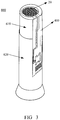
- FIG 3 is a perspective view illustrating the adhering method of a sticker with IC tag 400 involved in the present embodiment of the present disclosure.
- the covered container 600 is a bottle such as a wine bottle that includes a cork as a cover 610 and a container body 620.
- the sticker with IC tag 400 is adhered to the covered container 600 so that the single-stroke line portion 20 is adhered on the upper surface of the cover 610.
- Figure 3 discloses a situation where the single-stroke line portion 20 is adhered by covering a portion of the upper surface of the cover that corresponds to an inner side of the opening of the container, but it is not limited to this.
- the adhering can be performed by covering the whole upper surface of the cover.
- the IC tag insert is obscured by opaque tag paper, since the exact position of the single-stroke line portion is unknown, it is difficult to insert a needle without contacting the single-stroke line portion. Therefore, the single-stroke line portion can also be adhered to cover only a part of the upper surface of the cover.
- the IC chip 12 can detect disconnection of the single-stroke line portion 20 and detect malicious needle traces so as to reliably prevent the occurrence of inserting a needle into the cork for illegal replacement of the contained object.
- a bottle having a cork such as a wine bottle is illustrated as an example of the covered container
- the use of the sticker with IC tag of the present disclosure is not limited to this.
- the sticker with IC tag of the present disclosure may also be applied for example to a container having a thinner aluminum cover, a container having a upper surface into which a needle may be easily inserted, etc.
- Figure 4 is an enlarged view illustrating a construction of a single-stroke line portion involved in the present embodiment of the present disclosure, and corresponding to the area Q shown in Figures 1 and 2 .
- the single-stroke line portion 20 is formed by bending one line 50 into a zigzag shape. As shown in Figure 4 , for example, under the situation that the widths of two adjacent lines 50 of the single-stroke line portion 20 are respectively set to a and a', the gap 51 between the two lines 50 is set to b, and the diameter of the needle 62 is set to c, in order to reliably disconnect the lines 50 of the single-stroke line portion 20 when the needle 62 is inserted, the sum of the widths a and a' of the two lines 50 and the gap b between the two lines 50 must be less than or equal to the diameter c of the needle 62. That is, a+a'+b ⁇ c shall be met.
- the sum of the widths (a+a') of the two lines 50 and the gap b between the two lines 50, a+a'+b is set to be a value within 0.225mm to 3mm.
- the widths of the two lines 50 that is, a and a', can be equal, and can be not equal.
- the first embodiment described above enumerates a circuit pattern formed by bending one line into a zigzag shape, but it is not limited to this.
- the circuit patterns shown in Figures 5 and 6 can also be used.
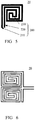
- Figure 5 is a schematic diagram showing an example of a circuit pattern of the single-stroke line portion involved in a varied embodiment of the present disclosure.
- the two winding lines 210 and 220 are winded in parallel in the same direction, and ends of them at one side of the winding axis are connected with a connection line 230 so as to form the circuit pattern 200.
- circuit pattern of the single-stroke line portion 20 As shown in Fig. 6 , two circuit patterns having identical shapes as that shown in Figure 5 are connected to form the circuit pattern.
- spiral lines shown in Figures 7 and 8 can also be used to form a single-stroke line portion 20.
- FIG. 7 is a schematic diagram showing a further example of a circuit pattern 200 of the single-stroke line portion 20 involved in the varied embodiment of the present disclosure.
- the circuit pattern 200 is formed by one winding line.
- the circuit pattern 200 comprises a spiral portion 310, an inner circumference lead 320 drawn from the inner circumference end portion of the spiral portion 310, and an outer circumference lead 330 drawn from the outer circumference end portion of the spiral portion 310.
- the circuit pattern 200 is formed on a double-sided single-layer substrate
- the inner circumference lead 320 is disposed on the back side of the substrate
- the outer circumference lead 330 and the spiral portion 310 are disposed on a surface of the substrate.
- the single-stroke line portion 20 is formed by the following circuit pattern 200: one winding line is twisted into a spiral shape across the surface and the back of the double-sided single layer substrate.
- the inner circumference lead 320 is disposed on one layer of the substrate, and the outer circumference lead 330 and the spiral portion 310 are disposed on another layer of the substrate.
- the outer circumference lead 330 and the spiral portion 310 can be further disposed on different layers of the substrate.
- the single-stroke line portion 20 is formed by the following circuit pattern 200: one winding line is twisted into a spiral shape across the different layers of the multilayer substrate.
- circuit pattern of the single-stroke line portion 20 involved in the varied embodiment as shown in Fig. 8 , in the situation where the circuit pattern 200 is formed on a single-side single-layer substrate, it is only required to dispose an insulating layer between the inner circumference lead 320 and the spiral portion 310.
- the sum of the widths of the two adjacent lines and the distance between the two lines is preferred to be a value between 0.225mm to 3mm.
- a wine bottle with a cork is illustrated as an example of the container of the present disclosure in the above descriptions, it is not limited to this.
- the present disclosure may also be applied to beverage bottles, liquid seasoning bottles, etc.
Landscapes
- Engineering & Computer Science (AREA)
- Computer Hardware Design (AREA)
- Microelectronics & Electronic Packaging (AREA)
- Physics & Mathematics (AREA)
- General Physics & Mathematics (AREA)
- Theoretical Computer Science (AREA)
- Computer Security & Cryptography (AREA)
- General Engineering & Computer Science (AREA)
- Closures For Containers (AREA)
- Details Of Rigid Or Semi-Rigid Containers (AREA)
- Details Of Aerials (AREA)
- Labeling Devices (AREA)
Abstract
Description
- The present disclosure relates to a sticker with IC tag, and more specifically to a sticker with IC tag that can prevent the replacement of object contained in containers such as soft cork bottles and the like with counterfeit.
- In the past, the demand in a worldwide scope for goods management, logistics management, and authenticity determination of goods such as wines is increasing. As an IC tag used for goods management, logistics management, and true and false management, an RFID tag is known for communicating with a reader in a contactless manner so as to transfer information between the reader and the tag itself. An RFID tag is composed of an RFIC chip for processing wireless signals, and an antenna for transmitting and receiving the wireless signals. Specified information is transmitted and received between the antenna of the RFID tag and the antenna of the reader as high frequency signals through a magnetic field or electric wave.
- However, in order to prevent the unlawful opening of the wine bottle or the repeated use of the IC tag, the IC tag should be destroyed when the wine bottle is opened.
- As a technique used to destroy the IC tag when opening the wine bottle as described above, for example, Patent Document 1 discloses the following IC tag sticker and the adhering method thereof: that is, the antenna is installed as stretching across both a metal cover and a container body, the antenna is destroyed when the cover is opened, the opening of the metal cover is detected through the condition of the antenna being destroyed. In order to easily destroy the antenna easily when opening the cover, the IC tag sticker in Patent Document 1 adopts the following structure: namely, a brittle processing for cutting off a slit (or loop circuit) for impedance matching adjustment of the antenna is carried out.
- Patent Document 1:
WO2006/016559 - However, there is situation, for example, where a cover of a covered container such as a wine bottle is constituted of a cork. In addition, for a vintage wine, there is a tool for taking out the contained wine without pulling out the cork, and cases where the tool is maliciously used to replace genuine wine with counterfeit often occurred.
- On the other hand, as recited in for example Patent Document 1, even if the sticker with IC tag is installed on a side of a wine bottle so that the antenna stretches across both a cover portion and a container body, the antenna would not be destroyed when a tool such as needle is inserted from an upper surface of the cover. Therefore, malicious use of the above tool to replace genuine wine with counterfeit cannot be prevented.
- The present invention is implemented in view of the above-mentioned problem, and its purpose is to provide a sticker with IC tag which can detect conditions where a thinner tool is inserted from an upper surface of a cover of a covered container so as to prevent malicious replacement of the contained object.
- To solve the above-mentioned technical problem, a sticker with IC tag involved in the present disclosure comprises: an antenna portion; and an IC chip bonded with the antenna portion and having a function of communicating through the antenna portion. The sticker with IC tag is installed on a covered container, characterized in that the sticker with IC tag comprises a single-stroke line portion which is coupled to the IC chip and adhered on the upper surface of the cover of the covered container. The IC chip detects disconnection of the single-stroke line portion.
- According to the present disclosure, under the condition that a covered container has a cover such as a cork, a single-stroke line portion would be cut off when attempting to draw out contained object by inserting a tool such as a needle from an upper surface of the cover, and disconnection may be detected by use of the IC chip so as to reliably prevent malicious replacement of the contained object.
-
-
Figure 1 is a top view showing the structure of a sticker with IC tag in UHF band involved in the first embodiment of the present disclosure. -
Figure 2 is a top view showing the structure of a sticker with IC tag in HF band involved in the first embodiment of the present disclosure. -
Figure 3 is a perspective view illustrating the pasting method of a sticker with IC tag involved in the first embodiment of the present disclosure. -
Figure 4 is an enlarged view illustrating a construction of a single-stroke line portion involved in the second embodiment of the present disclosure. -
Figure 5 is a schematic diagram showing an example of a circuit pattern of the single-stroke line portion involved in a varied embodiment of the present disclosure. -
Figure 6 is a schematic diagram showing another example of a circuit pattern of the single-stroke line portion involved in the varied embodiment of the present disclosure. -
Figure 7 is a schematic diagram showing a further example of a circuit pattern of the single-stroke line portion involved in the varied embodiment of the present disclosure. -
Figure 8 is a schematic diagram showing a still further example of a circuit pattern of the single-stroke line portion involved in the varied embodiment of the present disclosure. - In the following descriptions, the first embodiment of the present disclosure will be explained with reference to
Figures 1 to 3 . -
Figure 1 is a top view showing the structure of a sticker withIC tag 400 in UHF band involved in the first embodiment of the present disclosure. As shown inFigure 1 , the sticker withIC tag 400 in UHF band comprises anIC tag insert 100, and a sheet-shaped tag paper 41 being a support for the sticker withIC tag 400. TheIC tag insert 100 comprises: aradiation element 10 being an antenna; a slit (or loop circuit) for impedance matching adjustment, which adjusts the impedance matching of the antenna characteristics; anIC chip 12, an end of which is coupled to the slit (or loop circuit) for impedance matching adjustment;disconnection detection circuit 13, which is coupled to the other end of theIC chip 12 and is constituted of a ring conductor; and asubstrate 14, which is sheet-shaped and becomes a support for theradiation element 10, the slit (or loop circuit) forimpedance matching adjustment 11, and thedisconnection detection circuit 13. In addition, theradiation element 10 and the slit (or loop circuit) forimpedance matching adjustment 11 form the antenna portion, which is used for communicating with an antenna of a reader (not illustrated). - In addition, the
disconnection detection circuit 13 comprises a single-stroke line portion 20 constituted of a single-stroke line shaped conductor. As an example of the circuit pattern of the single-stroke line portion 20, a circuit pattern formed by winding lines can be enumerated. For example, as shown inFig. 1 , a single-stroke line portion 20 is formed by using a circuit pattern formed by bending one line into a zigzag shape. - The
IC chip 12 has function of detecting on and off of thedisconnection detection circuit 13 including the single-stroke line portion 20, especially, detecting disconnection of the single-stroke line portion 20. In addition, in the sticker withIC tag 400 in UHF band of the present embodiment, theIC chip 12 utilizes UCODE G2iL+ produced by NXP Semiconductors Corporation, but it is not limited to this, an IC chip such as UCODE G2iM+ produced by NXP Semiconductors Corporation that detects disconnection using resistance of the disconnection detection circuit other than antenna terminals may also be utilized. -
Figure 2 is a top view showing the structure of a sticker with IC tag 400' in HF band involved in the present embodiment of the present disclosure. As shown inFigure 2 , the sticker with IC tag 400' in HF band comprises an IC tag insert 100', and a sheet-shaped tag paper 41 being a support for the sticker with IC tag 400'. The IC tag insert 100' comprises: a loop circuit forantenna 15; anIC chip 12, an end of which is coupled to the loop circuit forantenna 15;disconnection detection circuit 13, which is coupled to the other end of theIC chip 12 and is constituted of a ring conductor; and asubstrate 14, which is sheet-shaped and becomes a support for the loop circuit forantenna 15 and thedisconnection detection circuit 13. In addition, the loop circuit forantenna 15 forms the antenna portion, which is used for communicating with an antenna of a reader (not illustrated). - In addition, the
disconnection detection circuit 13 comprises a single-stroke line portion 20 formed by a winding shaped conductor. The structure of the single-stroke line portion 20 is identical to that shown inFigure 1 . - The IC chip 12' has the function of detecting on and off of the
disconnection detection circuit 13 including the single-stroke line portion 20. In addition, in the sticker with IC tag 400' in HF band in the present embodiment, the IC chip 12' utilizes ICODE SLIX produced by NXP Semiconductors Corporation, but it is not limited to this. - In addition, while
Figure 2 discloses a sticker with IC tag 400' in HF band that includes thedisconnection detection circuit 13, wherein the single-stroke line portion 20 is a part of thedisconnection detection circuit 13, there can be situations where nodisconnection detection circuit 13 is included but a part of the loop circuit forantenna 15 is used to form the single-stroke line portion. In other words, the single-stroke line portion can also be a part of the antenna. In this case, as an IC chip, not only a chip having terminals for antenna and terminals for detecting on and off of circuits may be used, but also a chip having only one pair of antenna terminals may be used. The IC chip detects disconnection of the single-stroke line portion based on whether or not it can communicate through the antenna portion. - Next, the adhering method of the sticker with IC tag of the present embodiment is illustrated.
-
Figure 3 is a perspective view illustrating the adhering method of a sticker withIC tag 400 involved in the present embodiment of the present disclosure. As shown inFigure 3 , the coveredcontainer 600 is a bottle such as a wine bottle that includes a cork as acover 610 and acontainer body 620. The sticker withIC tag 400 is adhered to the coveredcontainer 600 so that the single-stroke line portion 20 is adhered on the upper surface of thecover 610. - In addition,
Figure 3 discloses a situation where the single-stroke line portion 20 is adhered by covering a portion of the upper surface of the cover that corresponds to an inner side of the opening of the container, but it is not limited to this. For example, the adhering can be performed by covering the whole upper surface of the cover. Or, when the IC tag insert is obscured by opaque tag paper, since the exact position of the single-stroke line portion is unknown, it is difficult to insert a needle without contacting the single-stroke line portion. Therefore, the single-stroke line portion can also be adhered to cover only a part of the upper surface of the cover. - According to the structure of the present embodiment, for example, inserting a tool such as a needle into an upper surface of cover such as the cork will make disconnection of the single-
stroke line portion 20 happen. TheIC chip 12 can detect disconnection of the single-stroke line portion 20 and detect malicious needle traces so as to reliably prevent the occurrence of inserting a needle into the cork for illegal replacement of the contained object. - In addition, while in the present embodiment, a bottle having a cork such as a wine bottle is illustrated as an example of the covered container, the use of the sticker with IC tag of the present disclosure is not limited to this. The sticker with IC tag of the present disclosure may also be applied for example to a container having a thinner aluminum cover, a container having a upper surface into which a needle may be easily inserted, etc.
- In the following description, the second embodiment of the present disclosure will be explained with reference to
Figure 4 . -
Figure 4 is an enlarged view illustrating a construction of a single-stroke line portion involved in the present embodiment of the present disclosure, and corresponding to the area Q shown inFigures 1 and 2 . - The single-
stroke line portion 20 is formed by bending oneline 50 into a zigzag shape. As shown inFigure 4 , for example, under the situation that the widths of twoadjacent lines 50 of the single-stroke line portion 20 are respectively set to a and a', thegap 51 between the twolines 50 is set to b, and the diameter of theneedle 62 is set to c, in order to reliably disconnect thelines 50 of the single-stroke line portion 20 when theneedle 62 is inserted, the sum of the widths a and a' of the twolines 50 and the gap b between the twolines 50 must be less than or equal to the diameter c of theneedle 62. That is, a+a'+b≤c shall be met. As a specific example of the above structure, the sum of the widths (a+a') of the twolines 50 and the gap b between the twolines 50, a+a'+b, is set to be a value within 0.225mm to 3mm. In addition, the widths of the twolines 50, that is, a and a', can be equal, and can be not equal. - According to the structure of the present embodiment, even if the insertion position of a needle with a smaller diameter slightly deviates, still it can reliably cause the
line 50 to disconnect, so as to more reliably prevent the occurrence of illegal replacement of the contained object with a finer needle. - In the following description, the varied embodiment of the present disclosure will be explained with reference to
Figures 5 and 6 . - As an example of the circuit pattern of a single-stroke line portion formed by winding shaped lines, the first embodiment described above enumerates a circuit pattern formed by bending one line into a zigzag shape, but it is not limited to this. For example, the circuit patterns shown in
Figures 5 and 6 can also be used. -
Figure 5 is a schematic diagram showing an example of a circuit pattern of the single-stroke line portion involved in a varied embodiment of the present disclosure. As shown inFigure 5 , the two windinglines connection line 230 so as to form thecircuit pattern 200. - In addition, as another example of the circuit pattern of the single-
stroke line portion 20, as shown inFig. 6 , two circuit patterns having identical shapes as that shown inFigure 5 are connected to form the circuit pattern. - Besides, in addition to the winding lines, the spiral lines shown in
Figures 7 and 8 can also be used to form a single-stroke line portion 20. -
Figure 7 is a schematic diagram showing a further example of acircuit pattern 200 of the single-stroke line portion 20 involved in the varied embodiment of the present disclosure. As shown inFigure 7 , thecircuit pattern 200 is formed by one winding line. Thecircuit pattern 200 comprises aspiral portion 310, aninner circumference lead 320 drawn from the inner circumference end portion of thespiral portion 310, and anouter circumference lead 330 drawn from the outer circumference end portion of thespiral portion 310. - In the situation where the
circuit pattern 200 is formed on a double-sided single-layer substrate, for example, theinner circumference lead 320 is disposed on the back side of the substrate, and theouter circumference lead 330 and thespiral portion 310 are disposed on a surface of the substrate. In other words, the single-stroke line portion 20 is formed by the following circuit pattern 200: one winding line is twisted into a spiral shape across the surface and the back of the double-sided single layer substrate. - In addition, in the situation where the
circuit pattern 200 is formed on a multilayer substrate, for example, theinner circumference lead 320 is disposed on one layer of the substrate, and theouter circumference lead 330 and thespiral portion 310 are disposed on another layer of the substrate. In addition, theouter circumference lead 330 and thespiral portion 310 can be further disposed on different layers of the substrate. In other words, the single-stroke line portion 20 is formed by the following circuit pattern 200: one winding line is twisted into a spiral shape across the different layers of the multilayer substrate. - In addition, as a further example of the circuit pattern of the single-
stroke line portion 20 involved in the varied embodiment, as shown inFig. 8 , in the situation where thecircuit pattern 200 is formed on a single-side single-layer substrate, it is only required to dispose an insulating layer between theinner circumference lead 320 and thespiral portion 310. - In addition, for the circuit patterns of the above varied embodiments, it is preferred to set the sum of the widths of the two adjacent lines and the distance between the two lines to be a value between 0.225mm to 3mm.
- Further, while a wine bottle with a cork is illustrated as an example of the container of the present disclosure in the above descriptions, it is not limited to this. The present disclosure may also be applied to beverage bottles, liquid seasoning bottles, etc.
- The embodiments and varied embodiments of the present disclosure are illustrated above. However, various omissions, replacements, and modifications may be made within the scope of the idea of the present disclosure.
-
- 10 Radiation element
- 11 Slit (or loop circuit) for impedance matching adjustment
- 12 IC chip
- 13 Disconnection detection circuit
- 14 Substrate
- 15 Loop circuit for antenna
- 20 Single-stroke line portion
- 41 Tag paper
- 50 Lines
- 51 Gap
- 62 Needle
- 100, 100' IC tag insert
- 200 Circuit pattern
- 210, 220 Winding lines
- 230 Connection line
- 310 Spiral portion
- 320 Inner circumference lead
- 330 Outer circumference lead
- 400, 400' sticker with IC tag
- 600 Covered container
- 610 Cover portion
- 620 Container body
Claims (13)
- A sticker with IC tag comprising: an antenna portion; and an IC chip coupled to the antenna portion and having the function of communicating through the antenna portion, the sticker with IC tag being installed on a covered container, wherein,
the sticker with IC tag comprises a single-stroke line portion, which is coupled to the IC chip and adhered to an upper surface of a cover portion of the covered container,
the IC chip is to detect disconnection of the single-stroke line portion. - The sticker with IC tag as recited in claim 1, wherein,
the single-stroke line portion being formed by winding lines,
the sum of the widths of two adjacent lines and the distance between the lines is within 0.225mm to 3mm. - The sticker with IC tag as recited in claim 1, wherein,
the single-stroke line portion being formed by spiral lines,
the sum of the widths of two adjacent lines and the distance between the lines is within 0.225mm to 3mm. - The sticker with IC tag as recited in claim 1 or claim 2, wherein the single-stroke line portion being formed by the following circuit pattern: bending one line into a zigzag shape.
- The sticker with IC tag as recited in claim 1 or claim 2, wherein,
the single-stroke line portion being formed by the following circuit pattern: twisting two winding lines in parallel in the same direction and connecting ends of said two winding lines at one side of winding axis with a connection line. - The sticker with IC tag as recited in claim 1 or claim 2, wherein,
the single-stroke line portion being formed by connecting the following two circuit patterns: twisting two winding lines in parallel in the same direction and connecting ends of the two winding lines at the winding shaft side with a connection line. - The sticker with IC tag as recited in any of claims 1 to 3, wherein,
the single-stroke line portion being formed by the following circuit pattern: twisting one winding line into a spiral shape across the surface and the back of a two-side single-layer substrate. - The sticker with IC tag as recited in any of claims 1 to 3, wherein
the single-stroke line portion being formed by the following circuit pattern: twisting one winding line into a spiral shape across different layers of a multilayer substrate. - The sticker with IC tag as recited in any of claims 1 to 3, wherein,
the single-stroke line portion being formed by the following circuit pattern: twisting one winding line into a spiral shape on a side of a single-side single layer substrate ,
disposing an insulating layer between an inner circumference lead of the winding line and the spiral portion, the inner circumference lead being drawn from an inner circumference end portion of the winding line. - The sticker with IC tag as recited in any of claims 1 to 3, wherein,
the single-stroke line portion is adhered in a manner that at least a portion of an upper surface of the cover is covered, said portion corresponds to an inner side of the opening of the covered container. - The sticker with IC tag as recited in claim 10, wherein,
the single-stroke line portion is adhered in a manner that the whole upper surface of the cover is covered. - The sticker with IC tag as recited in any of claims 1 to 3, wherein,
the single-stroke line portion being a part of the antenna portion,
the IC chip is to detect disconnection of the single-stroke line portion based on whether or not the IC chip can communicate through the antenna portion. - A covered container having a sticker with IC tag as recited in any of claims 1 to 12 adhered thereto.
Applications Claiming Priority (2)
| Application Number | Priority Date | Filing Date | Title |
|---|---|---|---|
| CN201510566660.0A CN106503779A (en) | 2015-09-08 | 2015-09-08 | Band IC tag paster |
| PCT/CN2016/098406 WO2017041725A1 (en) | 2015-09-08 | 2016-09-08 | Sticker having an ic tag |
Publications (3)
| Publication Number | Publication Date |
|---|---|
| EP3349150A1 true EP3349150A1 (en) | 2018-07-18 |
| EP3349150A4 EP3349150A4 (en) | 2019-05-01 |
| EP3349150B1 EP3349150B1 (en) | 2022-06-15 |
Family
ID=58239156
Family Applications (1)
| Application Number | Title | Priority Date | Filing Date |
|---|---|---|---|
| EP16843663.2A Active EP3349150B1 (en) | 2015-09-08 | 2016-09-08 | Sticker having an ic tag |
Country Status (5)
| Country | Link |
|---|---|
| US (1) | US10878304B2 (en) |
| EP (1) | EP3349150B1 (en) |
| JP (1) | JP6922896B2 (en) |
| CN (2) | CN106503779A (en) |
| WO (1) | WO2017041725A1 (en) |
Families Citing this family (10)
| Publication number | Priority date | Publication date | Assignee | Title |
|---|---|---|---|---|
| CN106503778A (en) * | 2015-09-08 | 2017-03-15 | 凸版印刷株式会社 | Band IC tag paster and its installation method |
| CN106503779A (en) * | 2015-09-08 | 2017-03-15 | 凸版印刷株式会社 | Band IC tag paster |
| CN110088010B (en) | 2016-12-15 | 2020-10-27 | 凸版印刷株式会社 | Cap seal |
| WO2019093425A1 (en) * | 2017-11-09 | 2019-05-16 | 株式会社村田製作所 | Rfid tag reading method, rfid tag reading system, rfid tag reader device, and article |
| JP7147308B2 (en) * | 2018-07-13 | 2022-10-05 | 凸版印刷株式会社 | IC tag label sheet and IC tag label |
| CN110712851B (en) * | 2019-09-30 | 2020-12-08 | 永道射频技术股份有限公司 | RFID functional plastic bottle cap with highly-coupled enhanced antenna |
| CN111572992B (en) * | 2020-05-28 | 2024-02-02 | 中国工商银行股份有限公司 | Accommodation apparatus, control method, and system for transporting article |
| US12124905B1 (en) * | 2021-12-17 | 2024-10-22 | Wells Fargo Bank, N.A. | Transaction instrument with features for destruction and disposal |
| EP4508566A1 (en) * | 2022-04-14 | 2025-02-19 | Authena AG | Protective electronic tag |
| EP4589471A4 (en) * | 2022-09-12 | 2025-12-31 | Toppan Holdings Inc | Tamper detection label and container with label |
Family Cites Families (68)
| Publication number | Priority date | Publication date | Assignee | Title |
|---|---|---|---|---|
| DE1294251B (en) | 1963-12-17 | 1969-04-30 | Nackenheim Ver Kapselfab | Foil bottle capsule |
| US5126749A (en) * | 1989-08-25 | 1992-06-30 | Kaltner George W | Individually fed multiloop antennas for electronic security systems |
| JP2001202489A (en) * | 2000-01-20 | 2001-07-27 | Denso Corp | IC card and manufacturing method thereof |
| DE10012204A1 (en) * | 2000-03-13 | 2001-09-20 | Siemens Ag | Electronic postage stamp for identifying postal articles |
| US6703935B1 (en) * | 2001-05-14 | 2004-03-09 | Amerasia International Technology, Inc. | Antenna arrangement for RFID smart tags |
| JP4590161B2 (en) * | 2001-05-21 | 2010-12-01 | スコット・ラボラトリーズ・インコーポレイテッド | RF-ID label for medical container |
| WO2004030148A1 (en) * | 2002-09-30 | 2004-04-08 | The Furukawa Electric Co., Ltd. | Rfid tag and process for producing the same |
| ITMI20022121A1 (en) * | 2002-10-04 | 2004-04-05 | Fidereveuropa | ELECTRONIC PAPER WITH AT LEAST ONE ADHESIVE SURFACE. |
| FR2848990B1 (en) | 2002-12-23 | 2005-07-01 | Alsacienne Aluminium | BOTTLE COIFFE, IN PARTICULAR BOTTLE OF WINE OR CHAMPAGNE |
| US7864053B2 (en) * | 2006-04-12 | 2011-01-04 | Visible Assets, Inc. | Visibility radio cap and network |
| ATE530998T1 (en) * | 2003-07-07 | 2011-11-15 | Avery Dennison Corp | RFID DEVICE WITH CHANGEABLE CHARACTERISTICS |
| CN1898686A (en) * | 2003-12-24 | 2007-01-17 | 新加坡科技物资管理私人有限公司 | Rfid sealing label |
| JP4512389B2 (en) * | 2004-03-15 | 2010-07-28 | 株式会社岩田レーベル | Divided label for chemical container |
| US7254848B2 (en) * | 2004-04-01 | 2007-08-14 | Encon Safety Products, Inc. | Emergency eye wash system |
| US7098794B2 (en) | 2004-04-30 | 2006-08-29 | Kimberly-Clark Worldwide, Inc. | Deactivating a data tag for user privacy or tamper-evident packaging |
| JP3105286U (en) | 2004-05-17 | 2004-10-28 | 富士光電株式会社 | Structure of a container having a feature that a wireless IC tag is destroyed during use |
| CN101001792B (en) | 2004-08-09 | 2011-03-30 | 凸版印刷株式会社 | Seal with IC label and its installation method |
| US20060145870A1 (en) * | 2004-10-19 | 2006-07-06 | Coveley Michael E | Container including a tamper-resistant seal and to a radio frequency identification seal |
| JP2006123917A (en) | 2004-10-26 | 2006-05-18 | Mitsubishi Materials Corp | Sealing structure, opening discrimination method, and tag |
| JP2006184082A (en) * | 2004-12-27 | 2006-07-13 | Hitachi Ltd | Sealing method and sealing confirmation system for radioactive material storage container |
| US20060152364A1 (en) * | 2004-12-30 | 2006-07-13 | Walton Charles A | RFID with field changeable identification |
| US20060214789A1 (en) | 2005-03-24 | 2006-09-28 | Joshua Posamentier | Tamper detection with RFID tag |
| DE202004021343U1 (en) * | 2005-04-18 | 2007-10-25 | Huhtamaki Ronsberg, Zweigniederlassung Der Huhtamaki Deutschland Gmbh & Co. Kg | Printed carrier substrate |
| EP1908032A4 (en) * | 2005-07-19 | 2011-02-02 | Prec Dynamics Corp | Semi-active rfid tag and related processes |
| JP4826195B2 (en) * | 2005-09-30 | 2011-11-30 | 大日本印刷株式会社 | RFID tag |
| US7652575B2 (en) * | 2005-10-27 | 2010-01-26 | Hewlett-Packard Development Company, L.P. | Monitoring of packages |
| US20070262866A1 (en) * | 2005-11-14 | 2007-11-15 | Ronald Eveland | Multi-Dimensional Broadband Track and Trace Sensor Radio Frequency Identification Device |
| US7388506B2 (en) * | 2006-02-07 | 2008-06-17 | Rexam Healthcare Packaging Inc. | Closure and package with induction seal and RFID tag |
| KR100764105B1 (en) * | 2006-02-28 | 2007-10-08 | 주식회사 손텍 | Radio Frequency Identification Label and Ceramic Patch Antenna |
| US7410103B2 (en) * | 2006-03-13 | 2008-08-12 | Andreas Rolf Nagel | System, method and device to detect product tampering |
| US20070273532A1 (en) * | 2006-05-17 | 2007-11-29 | Tagsys Sas | RFID tag for conductive surface |
| US20090045959A1 (en) * | 2007-08-16 | 2009-02-19 | Lottabase, Llc. | Beverage container authenticity and provenance devices and methods |
| JP2008143589A (en) * | 2006-12-13 | 2008-06-26 | Dainippon Printing Co Ltd | Packaging package with IC tag |
| US7898422B2 (en) * | 2007-10-18 | 2011-03-01 | Wine Father LLC | Tamper-resistant microchip assembly |
| WO2009050662A1 (en) * | 2007-10-19 | 2009-04-23 | Petratec International Ltd. | Rfid tag especially for use near conductive objects |
| US7782212B2 (en) * | 2007-12-14 | 2010-08-24 | Avery Dennison Corporation | Radio frequency sealing apparatus for a container |
| EP2301857B1 (en) | 2008-06-20 | 2012-08-29 | Toyo Seikan Kaisha, Ltd. | Resin overcap provided with ic tag |
| US8706628B2 (en) * | 2009-02-25 | 2014-04-22 | Mastercard International Incorporated | Automated opening of electronic wallet function in mobile device |
| EP2372676B1 (en) * | 2010-03-29 | 2017-03-15 | Deutsche Post AG | A sealing system for sealing of doors of transport vehicles |
| EP2558381B1 (en) * | 2010-04-14 | 2018-03-28 | Eagile, Inc. | Container seal with radio frequency identification tag. |
| US8937550B2 (en) * | 2010-04-14 | 2015-01-20 | Eagile, Inc. | Container seal with radio frequency identification tag, and method of making same |
| US20110285507A1 (en) * | 2010-05-21 | 2011-11-24 | Nelson Erik T | Tamper Detection RFID Tape |
| US8308073B2 (en) * | 2010-06-15 | 2012-11-13 | Convergence Systems Limited | Radio frequency identification (RFID) tag |
| US8746577B2 (en) * | 2010-09-20 | 2014-06-10 | The Board Of Trustees Of The University Of Illinois | Placement insensitive antenna for RFID, sensing, and/or communication systems |
| JP5803538B2 (en) * | 2011-10-06 | 2015-11-04 | 凸版印刷株式会社 | Container with IC tag and lid member with IC tag |
| JP5639606B2 (en) * | 2012-02-27 | 2014-12-10 | 三智商事株式会社 | Wireless IC tag |
| CN202529311U (en) * | 2012-04-05 | 2012-11-14 | 四川省宜宾五粮液集团有限公司 | Anti-counterfeiting structure of bottle cover |
| TWM440942U (en) * | 2012-05-11 | 2012-11-11 | Wander Plastic Co | Anti-counterfeiting bottle cap |
| JP5943735B2 (en) * | 2012-06-25 | 2016-07-05 | 東洋製罐株式会社 | Packaging container with IC tag |
| CN104411597B (en) * | 2012-06-25 | 2016-08-17 | 东洋制罐集团控股株式会社 | There is the clad vessel lid of IC tag |
| US9934895B2 (en) * | 2012-06-29 | 2018-04-03 | Intel Corporation | Spiral near field communication (NFC) coil for consistent coupling with different tags and devices |
| WO2014053005A1 (en) * | 2012-10-01 | 2014-04-10 | Tagsys Sas | Improvements in rfid tag assemblies and process |
| JP6303261B2 (en) | 2012-12-12 | 2018-04-04 | 東洋製罐株式会社 | Overcap and container with overcap |
| JP6265203B2 (en) * | 2013-02-19 | 2018-01-24 | 凸版印刷株式会社 | container |
| TW201525875A (en) * | 2013-12-19 | 2015-07-01 | 速碼波科技股份有限公司 | Security label |
| CN203673507U (en) * | 2014-01-09 | 2014-06-25 | 四川谦泰仁投资管理有限公司 | RFID electronic label used for container bottle |
| ES2940932T3 (en) | 2014-01-30 | 2023-05-12 | Americo Coelho Relvas Sucessores S A | Metal screw cap for bottle |
| US20150266634A1 (en) | 2014-03-19 | 2015-09-24 | Fang-Lin YANG | Bottle cap and container with bottle cap |
| FR3021438B1 (en) | 2014-05-21 | 2016-06-24 | Inside Secure | DOUBLE MODE ANTI-COUNTERFACON LABEL |
| FR3021439B1 (en) | 2014-05-21 | 2018-02-02 | Wisekey Semiconductors | ANTI-COUNTERFEIT LABEL THAT PRESERVES FUNCTIONALITY AFTER USE |
| US20160023812A1 (en) | 2014-07-24 | 2016-01-28 | Christopher Raymond Kikel | Reusable Sealing Bottle Cap Assembly |
| CN104217241A (en) * | 2014-08-21 | 2014-12-17 | 安徽云盾信息技术有限公司 | Electronic anti-fake label and realizing method |
| US9495851B1 (en) | 2014-11-25 | 2016-11-15 | Amazon Technologies, Inc. | Tag-based product monitoring and evaluation |
| US10035631B2 (en) * | 2014-12-05 | 2018-07-31 | Integrated Liner Technologies, Inc. | Tagged products and tracking thereof using customizable data points |
| CN204360408U (en) * | 2014-12-31 | 2015-05-27 | 上海动联信息技术股份有限公司 | A kind of drinks Anti-scrape label |
| US9471817B1 (en) * | 2015-07-09 | 2016-10-18 | Raed H. AlHazme | Action-triggered radio-frequency identification tag |
| CN106503779A (en) * | 2015-09-08 | 2017-03-15 | 凸版印刷株式会社 | Band IC tag paster |
| US10071916B2 (en) | 2015-10-15 | 2018-09-11 | Three Sevens Llc | Bottle cap with integrated frequency transmitter |
-
2015
- 2015-09-08 CN CN201510566660.0A patent/CN106503779A/en active Pending
-
2016
- 2016-09-08 CN CN201680041649.5A patent/CN107851209B/en active Active
- 2016-09-08 JP JP2018509538A patent/JP6922896B2/en active Active
- 2016-09-08 EP EP16843663.2A patent/EP3349150B1/en active Active
- 2016-09-08 WO PCT/CN2016/098406 patent/WO2017041725A1/en not_active Ceased
-
2018
- 2018-03-06 US US15/913,490 patent/US10878304B2/en active Active
Also Published As
| Publication number | Publication date |
|---|---|
| EP3349150A4 (en) | 2019-05-01 |
| JP6922896B2 (en) | 2021-08-18 |
| CN107851209A (en) | 2018-03-27 |
| WO2017041725A1 (en) | 2017-03-16 |
| JP2018532179A (en) | 2018-11-01 |
| EP3349150B1 (en) | 2022-06-15 |
| CN107851209B (en) | 2022-02-18 |
| CN106503779A (en) | 2017-03-15 |
| US20180197060A1 (en) | 2018-07-12 |
| US10878304B2 (en) | 2020-12-29 |
Similar Documents
| Publication | Publication Date | Title |
|---|---|---|
| US10878304B2 (en) | Sticker with IC tag | |
| US10489699B2 (en) | Sticker with IC tag and installation method thereof | |
| US8593258B2 (en) | High-tensile belt-type tag and wireless radio frequency identification system employing the same | |
| US10586143B2 (en) | Metal cap with RFID tag and container comprising same | |
| US10282572B2 (en) | Method for preventing unauthorized diversion of NFC tags | |
| CA2542043C (en) | Bottle cap | |
| EP3279837B1 (en) | Electronic tamper detection device | |
| JP2006123917A (en) | Sealing structure, opening discrimination method, and tag | |
| CN109492725B (en) | A label and anti-counterfeiting method | |
| CN102156903A (en) | Disassembly preventing electronic tag | |
| GB2521857A (en) | UHF RFID tag for bottles wines spirits has radio tamper evident means | |
| CN203673507U (en) | RFID electronic label used for container bottle | |
| EP3696732A1 (en) | Ic tag label | |
| US20150076235A1 (en) | Chipless nanotube electromagnetic identification system for anti-counterfeiting, authorization, and brand protection | |
| CN103426018A (en) | Wireless tag | |
| WO2018110602A1 (en) | Cap seal | |
| JP5092789B2 (en) | Label, sheet-like non-contact data carrier | |
| EP2251931A1 (en) | Structure having an antenna incorporated therein | |
| CN218825555U (en) | Novel double-frequency anti-counterfeiting electronic tag | |
| CN112644883A (en) | Manufacturing method of chip anti-counterfeiting intelligent package with detection function | |
| CN219590838U (en) | Novel high-frequency NFC tag antenna structure with on-off detection line | |
| CN210348539U (en) | Anti-fake label and anti-fake package | |
| EP1727078A1 (en) | IC chip for contactless identification system | |
| US20100156744A1 (en) | Antenna using buildup structure and method of manufacturing the same | |
| JP2015225577A (en) | Electronic passport |
Legal Events
| Date | Code | Title | Description |
|---|---|---|---|
| STAA | Information on the status of an ep patent application or granted ep patent |
Free format text: STATUS: THE INTERNATIONAL PUBLICATION HAS BEEN MADE |
|
| PUAI | Public reference made under article 153(3) epc to a published international application that has entered the european phase |
Free format text: ORIGINAL CODE: 0009012 |
|
| STAA | Information on the status of an ep patent application or granted ep patent |
Free format text: STATUS: REQUEST FOR EXAMINATION WAS MADE |
|
| 17P | Request for examination filed |
Effective date: 20180220 |
|
| AK | Designated contracting states |
Kind code of ref document: A1 Designated state(s): AL AT BE BG CH CY CZ DE DK EE ES FI FR GB GR HR HU IE IS IT LI LT LU LV MC MK MT NL NO PL PT RO RS SE SI SK SM TR |
|
| AX | Request for extension of the european patent |
Extension state: BA ME |
|
| DAV | Request for validation of the european patent (deleted) | ||
| DAX | Request for extension of the european patent (deleted) | ||
| REG | Reference to a national code |
Ref country code: DE Ref legal event code: R079 Ref document number: 602016072897 Country of ref document: DE Free format text: PREVIOUS MAIN CLASS: G06K0019073000 Ipc: G06K0019077000 |
|
| A4 | Supplementary search report drawn up and despatched |
Effective date: 20190329 |
|
| RIC1 | Information provided on ipc code assigned before grant |
Ipc: G06K 19/073 20060101ALI20190325BHEP Ipc: G06K 19/077 20060101AFI20190325BHEP Ipc: G06K 19/07 20060101ALI20190325BHEP |
|
| STAA | Information on the status of an ep patent application or granted ep patent |
Free format text: STATUS: EXAMINATION IS IN PROGRESS |
|
| 17Q | First examination report despatched |
Effective date: 20200430 |
|
| GRAP | Despatch of communication of intention to grant a patent |
Free format text: ORIGINAL CODE: EPIDOSNIGR1 |
|
| STAA | Information on the status of an ep patent application or granted ep patent |
Free format text: STATUS: GRANT OF PATENT IS INTENDED |
|
| INTG | Intention to grant announced |
Effective date: 20220331 |
|
| GRAS | Grant fee paid |
Free format text: ORIGINAL CODE: EPIDOSNIGR3 |
|
| GRAA | (expected) grant |
Free format text: ORIGINAL CODE: 0009210 |
|
| STAA | Information on the status of an ep patent application or granted ep patent |
Free format text: STATUS: THE PATENT HAS BEEN GRANTED |
|
| AK | Designated contracting states |
Kind code of ref document: B1 Designated state(s): AL AT BE BG CH CY CZ DE DK EE ES FI FR GB GR HR HU IE IS IT LI LT LU LV MC MK MT NL NO PL PT RO RS SE SI SK SM TR |
|
| REG | Reference to a national code |
Ref country code: CH Ref legal event code: EP Ref country code: GB Ref legal event code: FG4D |
|
| REG | Reference to a national code |
Ref country code: IE Ref legal event code: FG4D |
|
| REG | Reference to a national code |
Ref country code: DE Ref legal event code: R096 Ref document number: 602016072897 Country of ref document: DE |
|
| REG | Reference to a national code |
Ref country code: AT Ref legal event code: REF Ref document number: 1498825 Country of ref document: AT Kind code of ref document: T Effective date: 20220715 |
|
| REG | Reference to a national code |
Ref country code: LT Ref legal event code: MG9D |
|
| REG | Reference to a national code |
Ref country code: NL Ref legal event code: MP Effective date: 20220615 |
|
| PG25 | Lapsed in a contracting state [announced via postgrant information from national office to epo] |
Ref country code: SE Free format text: LAPSE BECAUSE OF FAILURE TO SUBMIT A TRANSLATION OF THE DESCRIPTION OR TO PAY THE FEE WITHIN THE PRESCRIBED TIME-LIMIT Effective date: 20220615 Ref country code: NO Free format text: LAPSE BECAUSE OF FAILURE TO SUBMIT A TRANSLATION OF THE DESCRIPTION OR TO PAY THE FEE WITHIN THE PRESCRIBED TIME-LIMIT Effective date: 20220915 Ref country code: LT Free format text: LAPSE BECAUSE OF FAILURE TO SUBMIT A TRANSLATION OF THE DESCRIPTION OR TO PAY THE FEE WITHIN THE PRESCRIBED TIME-LIMIT Effective date: 20220615 Ref country code: HR Free format text: LAPSE BECAUSE OF FAILURE TO SUBMIT A TRANSLATION OF THE DESCRIPTION OR TO PAY THE FEE WITHIN THE PRESCRIBED TIME-LIMIT Effective date: 20220615 Ref country code: GR Free format text: LAPSE BECAUSE OF FAILURE TO SUBMIT A TRANSLATION OF THE DESCRIPTION OR TO PAY THE FEE WITHIN THE PRESCRIBED TIME-LIMIT Effective date: 20220916 Ref country code: FI Free format text: LAPSE BECAUSE OF FAILURE TO SUBMIT A TRANSLATION OF THE DESCRIPTION OR TO PAY THE FEE WITHIN THE PRESCRIBED TIME-LIMIT Effective date: 20220615 Ref country code: BG Free format text: LAPSE BECAUSE OF FAILURE TO SUBMIT A TRANSLATION OF THE DESCRIPTION OR TO PAY THE FEE WITHIN THE PRESCRIBED TIME-LIMIT Effective date: 20220915 |
|
| REG | Reference to a national code |
Ref country code: AT Ref legal event code: MK05 Ref document number: 1498825 Country of ref document: AT Kind code of ref document: T Effective date: 20220615 |
|
| PG25 | Lapsed in a contracting state [announced via postgrant information from national office to epo] |
Ref country code: RS Free format text: LAPSE BECAUSE OF FAILURE TO SUBMIT A TRANSLATION OF THE DESCRIPTION OR TO PAY THE FEE WITHIN THE PRESCRIBED TIME-LIMIT Effective date: 20220615 Ref country code: LV Free format text: LAPSE BECAUSE OF FAILURE TO SUBMIT A TRANSLATION OF THE DESCRIPTION OR TO PAY THE FEE WITHIN THE PRESCRIBED TIME-LIMIT Effective date: 20220615 |
|
| PG25 | Lapsed in a contracting state [announced via postgrant information from national office to epo] |
Ref country code: NL Free format text: LAPSE BECAUSE OF FAILURE TO SUBMIT A TRANSLATION OF THE DESCRIPTION OR TO PAY THE FEE WITHIN THE PRESCRIBED TIME-LIMIT Effective date: 20220615 |
|
| PG25 | Lapsed in a contracting state [announced via postgrant information from national office to epo] |
Ref country code: SM Free format text: LAPSE BECAUSE OF FAILURE TO SUBMIT A TRANSLATION OF THE DESCRIPTION OR TO PAY THE FEE WITHIN THE PRESCRIBED TIME-LIMIT Effective date: 20220615 Ref country code: SK Free format text: LAPSE BECAUSE OF FAILURE TO SUBMIT A TRANSLATION OF THE DESCRIPTION OR TO PAY THE FEE WITHIN THE PRESCRIBED TIME-LIMIT Effective date: 20220615 Ref country code: RO Free format text: LAPSE BECAUSE OF FAILURE TO SUBMIT A TRANSLATION OF THE DESCRIPTION OR TO PAY THE FEE WITHIN THE PRESCRIBED TIME-LIMIT Effective date: 20220615 Ref country code: PT Free format text: LAPSE BECAUSE OF FAILURE TO SUBMIT A TRANSLATION OF THE DESCRIPTION OR TO PAY THE FEE WITHIN THE PRESCRIBED TIME-LIMIT Effective date: 20221017 Ref country code: ES Free format text: LAPSE BECAUSE OF FAILURE TO SUBMIT A TRANSLATION OF THE DESCRIPTION OR TO PAY THE FEE WITHIN THE PRESCRIBED TIME-LIMIT Effective date: 20220615 Ref country code: EE Free format text: LAPSE BECAUSE OF FAILURE TO SUBMIT A TRANSLATION OF THE DESCRIPTION OR TO PAY THE FEE WITHIN THE PRESCRIBED TIME-LIMIT Effective date: 20220615 Ref country code: CZ Free format text: LAPSE BECAUSE OF FAILURE TO SUBMIT A TRANSLATION OF THE DESCRIPTION OR TO PAY THE FEE WITHIN THE PRESCRIBED TIME-LIMIT Effective date: 20220615 Ref country code: AT Free format text: LAPSE BECAUSE OF FAILURE TO SUBMIT A TRANSLATION OF THE DESCRIPTION OR TO PAY THE FEE WITHIN THE PRESCRIBED TIME-LIMIT Effective date: 20220615 |
|
| PG25 | Lapsed in a contracting state [announced via postgrant information from national office to epo] |
Ref country code: PL Free format text: LAPSE BECAUSE OF FAILURE TO SUBMIT A TRANSLATION OF THE DESCRIPTION OR TO PAY THE FEE WITHIN THE PRESCRIBED TIME-LIMIT Effective date: 20220615 Ref country code: IS Free format text: LAPSE BECAUSE OF FAILURE TO SUBMIT A TRANSLATION OF THE DESCRIPTION OR TO PAY THE FEE WITHIN THE PRESCRIBED TIME-LIMIT Effective date: 20221015 |
|
| REG | Reference to a national code |
Ref country code: DE Ref legal event code: R097 Ref document number: 602016072897 Country of ref document: DE |
|
| PG25 | Lapsed in a contracting state [announced via postgrant information from national office to epo] |
Ref country code: AL Free format text: LAPSE BECAUSE OF FAILURE TO SUBMIT A TRANSLATION OF THE DESCRIPTION OR TO PAY THE FEE WITHIN THE PRESCRIBED TIME-LIMIT Effective date: 20220615 |
|
| PLBE | No opposition filed within time limit |
Free format text: ORIGINAL CODE: 0009261 |
|
| STAA | Information on the status of an ep patent application or granted ep patent |
Free format text: STATUS: NO OPPOSITION FILED WITHIN TIME LIMIT |
|
| PG25 | Lapsed in a contracting state [announced via postgrant information from national office to epo] |
Ref country code: MC Free format text: LAPSE BECAUSE OF FAILURE TO SUBMIT A TRANSLATION OF THE DESCRIPTION OR TO PAY THE FEE WITHIN THE PRESCRIBED TIME-LIMIT Effective date: 20220615 Ref country code: DK Free format text: LAPSE BECAUSE OF FAILURE TO SUBMIT A TRANSLATION OF THE DESCRIPTION OR TO PAY THE FEE WITHIN THE PRESCRIBED TIME-LIMIT Effective date: 20220615 |
|
| REG | Reference to a national code |
Ref country code: CH Ref legal event code: PL |
|
| 26N | No opposition filed |
Effective date: 20230316 |
|
| GBPC | Gb: european patent ceased through non-payment of renewal fee |
Effective date: 20220915 |
|
| REG | Reference to a national code |
Ref country code: BE Ref legal event code: MM Effective date: 20220930 |
|
| PG25 | Lapsed in a contracting state [announced via postgrant information from national office to epo] |
Ref country code: SI Free format text: LAPSE BECAUSE OF FAILURE TO SUBMIT A TRANSLATION OF THE DESCRIPTION OR TO PAY THE FEE WITHIN THE PRESCRIBED TIME-LIMIT Effective date: 20220615 |
|
| PG25 | Lapsed in a contracting state [announced via postgrant information from national office to epo] |
Ref country code: LU Free format text: LAPSE BECAUSE OF NON-PAYMENT OF DUE FEES Effective date: 20220908 |
|
| P01 | Opt-out of the competence of the unified patent court (upc) registered |
Effective date: 20230530 |
|
| PG25 | Lapsed in a contracting state [announced via postgrant information from national office to epo] |
Ref country code: LI Free format text: LAPSE BECAUSE OF NON-PAYMENT OF DUE FEES Effective date: 20220930 Ref country code: IE Free format text: LAPSE BECAUSE OF NON-PAYMENT OF DUE FEES Effective date: 20220908 Ref country code: CH Free format text: LAPSE BECAUSE OF NON-PAYMENT OF DUE FEES Effective date: 20220930 |
|
| PG25 | Lapsed in a contracting state [announced via postgrant information from national office to epo] |
Ref country code: BE Free format text: LAPSE BECAUSE OF NON-PAYMENT OF DUE FEES Effective date: 20220930 |
|
| PG25 | Lapsed in a contracting state [announced via postgrant information from national office to epo] |
Ref country code: GB Free format text: LAPSE BECAUSE OF NON-PAYMENT OF DUE FEES Effective date: 20220915 |
|
| PG25 | Lapsed in a contracting state [announced via postgrant information from national office to epo] |
Ref country code: IT Free format text: LAPSE BECAUSE OF FAILURE TO SUBMIT A TRANSLATION OF THE DESCRIPTION OR TO PAY THE FEE WITHIN THE PRESCRIBED TIME-LIMIT Effective date: 20220615 |
|
| PG25 | Lapsed in a contracting state [announced via postgrant information from national office to epo] |
Ref country code: HU Free format text: LAPSE BECAUSE OF FAILURE TO SUBMIT A TRANSLATION OF THE DESCRIPTION OR TO PAY THE FEE WITHIN THE PRESCRIBED TIME-LIMIT; INVALID AB INITIO Effective date: 20160908 |
|
| PG25 | Lapsed in a contracting state [announced via postgrant information from national office to epo] |
Ref country code: CY Free format text: LAPSE BECAUSE OF FAILURE TO SUBMIT A TRANSLATION OF THE DESCRIPTION OR TO PAY THE FEE WITHIN THE PRESCRIBED TIME-LIMIT Effective date: 20220615 |
|
| PG25 | Lapsed in a contracting state [announced via postgrant information from national office to epo] |
Ref country code: MK Free format text: LAPSE BECAUSE OF FAILURE TO SUBMIT A TRANSLATION OF THE DESCRIPTION OR TO PAY THE FEE WITHIN THE PRESCRIBED TIME-LIMIT Effective date: 20220615 |
|
| PG25 | Lapsed in a contracting state [announced via postgrant information from national office to epo] |
Ref country code: TR Free format text: LAPSE BECAUSE OF FAILURE TO SUBMIT A TRANSLATION OF THE DESCRIPTION OR TO PAY THE FEE WITHIN THE PRESCRIBED TIME-LIMIT Effective date: 20220615 |
|
| PG25 | Lapsed in a contracting state [announced via postgrant information from national office to epo] |
Ref country code: MT Free format text: LAPSE BECAUSE OF FAILURE TO SUBMIT A TRANSLATION OF THE DESCRIPTION OR TO PAY THE FEE WITHIN THE PRESCRIBED TIME-LIMIT Effective date: 20220615 |
|
| PG25 | Lapsed in a contracting state [announced via postgrant information from national office to epo] |
Ref country code: BG Free format text: LAPSE BECAUSE OF FAILURE TO SUBMIT A TRANSLATION OF THE DESCRIPTION OR TO PAY THE FEE WITHIN THE PRESCRIBED TIME-LIMIT Effective date: 20220615 |
|
| PG25 | Lapsed in a contracting state [announced via postgrant information from national office to epo] |
Ref country code: BG Free format text: LAPSE BECAUSE OF FAILURE TO SUBMIT A TRANSLATION OF THE DESCRIPTION OR TO PAY THE FEE WITHIN THE PRESCRIBED TIME-LIMIT Effective date: 20220615 |
|
| PGFP | Annual fee paid to national office [announced via postgrant information from national office to epo] |
Ref country code: DE Payment date: 20250730 Year of fee payment: 10 |
|
| PGFP | Annual fee paid to national office [announced via postgrant information from national office to epo] |
Ref country code: FR Payment date: 20250808 Year of fee payment: 10 |