EP3338303B1 - Integrated device package comprising bridge in litho-etchable layer - Google Patents
Integrated device package comprising bridge in litho-etchable layer Download PDFInfo
- Publication number
- EP3338303B1 EP3338303B1 EP16730956.6A EP16730956A EP3338303B1 EP 3338303 B1 EP3338303 B1 EP 3338303B1 EP 16730956 A EP16730956 A EP 16730956A EP 3338303 B1 EP3338303 B1 EP 3338303B1
- Authority
- EP
- European Patent Office
- Prior art keywords
- layer
- die
- bridge
- implementations
- integrated device
- Prior art date
- Legal status (The legal status is an assumption and is not a legal conclusion. Google has not performed a legal analysis and makes no representation as to the accuracy of the status listed.)
- Active
Links
- 238000005538 encapsulation Methods 0.000 claims description 187
- 239000000758 substrate Substances 0.000 claims description 121
- 239000000463 material Substances 0.000 claims description 32
- 239000004593 Epoxy Substances 0.000 claims description 10
- 238000004891 communication Methods 0.000 claims description 9
- 239000002184 metal Substances 0.000 description 170
- 229910052751 metal Inorganic materials 0.000 description 170
- 238000000034 method Methods 0.000 description 127
- 229910000679 solder Inorganic materials 0.000 description 51
- 238000007747 plating Methods 0.000 description 38
- 229910052710 silicon Inorganic materials 0.000 description 18
- 239000010703 silicon Substances 0.000 description 18
- 238000010586 diagram Methods 0.000 description 15
- 229920002120 photoresistant polymer Polymers 0.000 description 12
- 238000001465 metallisation Methods 0.000 description 11
- XUIMIQQOPSSXEZ-UHFFFAOYSA-N Silicon Chemical compound [Si] XUIMIQQOPSSXEZ-UHFFFAOYSA-N 0.000 description 10
- 238000005137 deposition process Methods 0.000 description 8
- 238000005530 etching Methods 0.000 description 8
- 238000001259 photo etching Methods 0.000 description 7
- 239000000919 ceramic Substances 0.000 description 6
- 239000011521 glass Substances 0.000 description 6
- 238000005240 physical vapour deposition Methods 0.000 description 6
- 239000000654 additive Substances 0.000 description 5
- 238000000059 patterning Methods 0.000 description 5
- 238000005229 chemical vapour deposition Methods 0.000 description 4
- 239000004020 conductor Substances 0.000 description 3
- 239000004065 semiconductor Substances 0.000 description 3
- VXXBCDUYUQKWCK-UHFFFAOYSA-N 1,2,3,4,5-pentachloro-6-(3,4,5-trichlorophenyl)benzene Chemical compound ClC1=C(Cl)C(Cl)=CC(C=2C(=C(Cl)C(Cl)=C(Cl)C=2Cl)Cl)=C1 VXXBCDUYUQKWCK-UHFFFAOYSA-N 0.000 description 2
- RYGMFSIKBFXOCR-UHFFFAOYSA-N Copper Chemical compound [Cu] RYGMFSIKBFXOCR-UHFFFAOYSA-N 0.000 description 2
- 239000004642 Polyimide Substances 0.000 description 2
- 239000000853 adhesive Substances 0.000 description 2
- 230000001070 adhesive effect Effects 0.000 description 2
- 229910052802 copper Inorganic materials 0.000 description 2
- 239000010949 copper Substances 0.000 description 2
- 239000000945 filler Substances 0.000 description 2
- 238000001459 lithography Methods 0.000 description 2
- 229920002577 polybenzoxazole Polymers 0.000 description 2
- 229920001721 polyimide Polymers 0.000 description 2
- 238000007650 screen-printing Methods 0.000 description 2
- 239000000126 substance Substances 0.000 description 2
- 230000008878 coupling Effects 0.000 description 1
- 238000010168 coupling process Methods 0.000 description 1
- 238000005859 coupling reaction Methods 0.000 description 1
- 238000000151 deposition Methods 0.000 description 1
- 230000008021 deposition Effects 0.000 description 1
- 239000003989 dielectric material Substances 0.000 description 1
- 238000009826 distribution Methods 0.000 description 1
- 230000002708 enhancing effect Effects 0.000 description 1
- 238000004519 manufacturing process Methods 0.000 description 1
- 238000000206 photolithography Methods 0.000 description 1
Images


Classifications
-
- H—ELECTRICITY
- H01—ELECTRIC ELEMENTS
- H01L—SEMICONDUCTOR DEVICES NOT COVERED BY CLASS H10
- H01L23/00—Details of semiconductor or other solid state devices
- H01L23/52—Arrangements for conducting electric current within the device in operation from one component to another, i.e. interconnections, e.g. wires, lead frames
- H01L23/538—Arrangements for conducting electric current within the device in operation from one component to another, i.e. interconnections, e.g. wires, lead frames the interconnection structure between a plurality of semiconductor chips being formed on, or in, insulating substrates
- H01L23/5385—Assembly of a plurality of insulating substrates
-
- H—ELECTRICITY
- H01—ELECTRIC ELEMENTS
- H01L—SEMICONDUCTOR DEVICES NOT COVERED BY CLASS H10
- H01L23/00—Details of semiconductor or other solid state devices
- H01L23/48—Arrangements for conducting electric current to or from the solid state body in operation, e.g. leads, terminal arrangements ; Selection of materials therefor
- H01L23/481—Internal lead connections, e.g. via connections, feedthrough structures
-
- H—ELECTRICITY
- H01—ELECTRIC ELEMENTS
- H01L—SEMICONDUCTOR DEVICES NOT COVERED BY CLASS H10
- H01L23/00—Details of semiconductor or other solid state devices
- H01L23/52—Arrangements for conducting electric current within the device in operation from one component to another, i.e. interconnections, e.g. wires, lead frames
- H01L23/538—Arrangements for conducting electric current within the device in operation from one component to another, i.e. interconnections, e.g. wires, lead frames the interconnection structure between a plurality of semiconductor chips being formed on, or in, insulating substrates
- H01L23/5384—Conductive vias through the substrate with or without pins, e.g. buried coaxial conductors
-
- H—ELECTRICITY
- H01—ELECTRIC ELEMENTS
- H01L—SEMICONDUCTOR DEVICES NOT COVERED BY CLASS H10
- H01L24/00—Arrangements for connecting or disconnecting semiconductor or solid-state bodies; Methods or apparatus related thereto
- H01L24/01—Means for bonding being attached to, or being formed on, the surface to be connected, e.g. chip-to-package, die-attach, "first-level" interconnects; Manufacturing methods related thereto
- H01L24/10—Bump connectors ; Manufacturing methods related thereto
- H01L24/12—Structure, shape, material or disposition of the bump connectors prior to the connecting process
- H01L24/13—Structure, shape, material or disposition of the bump connectors prior to the connecting process of an individual bump connector
-
- H—ELECTRICITY
- H01—ELECTRIC ELEMENTS
- H01L—SEMICONDUCTOR DEVICES NOT COVERED BY CLASS H10
- H01L24/00—Arrangements for connecting or disconnecting semiconductor or solid-state bodies; Methods or apparatus related thereto
- H01L24/91—Methods for connecting semiconductor or solid state bodies including different methods provided for in two or more of groups H01L24/80 - H01L24/90
- H01L24/92—Specific sequence of method steps
-
- H—ELECTRICITY
- H01—ELECTRIC ELEMENTS
- H01L—SEMICONDUCTOR DEVICES NOT COVERED BY CLASS H10
- H01L25/00—Assemblies consisting of a plurality of individual semiconductor or other solid state devices ; Multistep manufacturing processes thereof
- H01L25/03—Assemblies consisting of a plurality of individual semiconductor or other solid state devices ; Multistep manufacturing processes thereof all the devices being of a type provided for in the same subgroup of groups H01L27/00 - H01L33/00, or in a single subclass of H10K, H10N, e.g. assemblies of rectifier diodes
- H01L25/04—Assemblies consisting of a plurality of individual semiconductor or other solid state devices ; Multistep manufacturing processes thereof all the devices being of a type provided for in the same subgroup of groups H01L27/00 - H01L33/00, or in a single subclass of H10K, H10N, e.g. assemblies of rectifier diodes the devices not having separate containers
- H01L25/065—Assemblies consisting of a plurality of individual semiconductor or other solid state devices ; Multistep manufacturing processes thereof all the devices being of a type provided for in the same subgroup of groups H01L27/00 - H01L33/00, or in a single subclass of H10K, H10N, e.g. assemblies of rectifier diodes the devices not having separate containers the devices being of a type provided for in group H01L27/00
- H01L25/0655—Assemblies consisting of a plurality of individual semiconductor or other solid state devices ; Multistep manufacturing processes thereof all the devices being of a type provided for in the same subgroup of groups H01L27/00 - H01L33/00, or in a single subclass of H10K, H10N, e.g. assemblies of rectifier diodes the devices not having separate containers the devices being of a type provided for in group H01L27/00 the devices being arranged next to each other
-
- H—ELECTRICITY
- H01—ELECTRIC ELEMENTS
- H01L—SEMICONDUCTOR DEVICES NOT COVERED BY CLASS H10
- H01L2224/00—Indexing scheme for arrangements for connecting or disconnecting semiconductor or solid-state bodies and methods related thereto as covered by H01L24/00
- H01L2224/01—Means for bonding being attached to, or being formed on, the surface to be connected, e.g. chip-to-package, die-attach, "first-level" interconnects; Manufacturing methods related thereto
- H01L2224/10—Bump connectors; Manufacturing methods related thereto
- H01L2224/12—Structure, shape, material or disposition of the bump connectors prior to the connecting process
- H01L2224/13—Structure, shape, material or disposition of the bump connectors prior to the connecting process of an individual bump connector
- H01L2224/13001—Core members of the bump connector
- H01L2224/13099—Material
- H01L2224/131—Material with a principal constituent of the material being a metal or a metalloid, e.g. boron [B], silicon [Si], germanium [Ge], arsenic [As], antimony [Sb], tellurium [Te] and polonium [Po], and alloys thereof
-
- H—ELECTRICITY
- H01—ELECTRIC ELEMENTS
- H01L—SEMICONDUCTOR DEVICES NOT COVERED BY CLASS H10
- H01L2224/00—Indexing scheme for arrangements for connecting or disconnecting semiconductor or solid-state bodies and methods related thereto as covered by H01L24/00
- H01L2224/01—Means for bonding being attached to, or being formed on, the surface to be connected, e.g. chip-to-package, die-attach, "first-level" interconnects; Manufacturing methods related thereto
- H01L2224/10—Bump connectors; Manufacturing methods related thereto
- H01L2224/15—Structure, shape, material or disposition of the bump connectors after the connecting process
- H01L2224/16—Structure, shape, material or disposition of the bump connectors after the connecting process of an individual bump connector
- H01L2224/161—Disposition
- H01L2224/16151—Disposition the bump connector connecting between a semiconductor or solid-state body and an item not being a semiconductor or solid-state body, e.g. chip-to-substrate, chip-to-passive
- H01L2224/16221—Disposition the bump connector connecting between a semiconductor or solid-state body and an item not being a semiconductor or solid-state body, e.g. chip-to-substrate, chip-to-passive the body and the item being stacked
- H01L2224/16225—Disposition the bump connector connecting between a semiconductor or solid-state body and an item not being a semiconductor or solid-state body, e.g. chip-to-substrate, chip-to-passive the body and the item being stacked the item being non-metallic, e.g. insulating substrate with or without metallisation
- H01L2224/16227—Disposition the bump connector connecting between a semiconductor or solid-state body and an item not being a semiconductor or solid-state body, e.g. chip-to-substrate, chip-to-passive the body and the item being stacked the item being non-metallic, e.g. insulating substrate with or without metallisation the bump connector connecting to a bond pad of the item
-
- H—ELECTRICITY
- H01—ELECTRIC ELEMENTS
- H01L—SEMICONDUCTOR DEVICES NOT COVERED BY CLASS H10
- H01L2224/00—Indexing scheme for arrangements for connecting or disconnecting semiconductor or solid-state bodies and methods related thereto as covered by H01L24/00
- H01L2224/01—Means for bonding being attached to, or being formed on, the surface to be connected, e.g. chip-to-package, die-attach, "first-level" interconnects; Manufacturing methods related thereto
- H01L2224/10—Bump connectors; Manufacturing methods related thereto
- H01L2224/15—Structure, shape, material or disposition of the bump connectors after the connecting process
- H01L2224/16—Structure, shape, material or disposition of the bump connectors after the connecting process of an individual bump connector
- H01L2224/161—Disposition
- H01L2224/16151—Disposition the bump connector connecting between a semiconductor or solid-state body and an item not being a semiconductor or solid-state body, e.g. chip-to-substrate, chip-to-passive
- H01L2224/16221—Disposition the bump connector connecting between a semiconductor or solid-state body and an item not being a semiconductor or solid-state body, e.g. chip-to-substrate, chip-to-passive the body and the item being stacked
- H01L2224/16225—Disposition the bump connector connecting between a semiconductor or solid-state body and an item not being a semiconductor or solid-state body, e.g. chip-to-substrate, chip-to-passive the body and the item being stacked the item being non-metallic, e.g. insulating substrate with or without metallisation
- H01L2224/16235—Disposition the bump connector connecting between a semiconductor or solid-state body and an item not being a semiconductor or solid-state body, e.g. chip-to-substrate, chip-to-passive the body and the item being stacked the item being non-metallic, e.g. insulating substrate with or without metallisation the bump connector connecting to a via metallisation of the item
-
- H—ELECTRICITY
- H01—ELECTRIC ELEMENTS
- H01L—SEMICONDUCTOR DEVICES NOT COVERED BY CLASS H10
- H01L2224/00—Indexing scheme for arrangements for connecting or disconnecting semiconductor or solid-state bodies and methods related thereto as covered by H01L24/00
- H01L2224/01—Means for bonding being attached to, or being formed on, the surface to be connected, e.g. chip-to-package, die-attach, "first-level" interconnects; Manufacturing methods related thereto
- H01L2224/26—Layer connectors, e.g. plate connectors, solder or adhesive layers; Manufacturing methods related thereto
- H01L2224/31—Structure, shape, material or disposition of the layer connectors after the connecting process
- H01L2224/32—Structure, shape, material or disposition of the layer connectors after the connecting process of an individual layer connector
- H01L2224/321—Disposition
- H01L2224/32151—Disposition the layer connector connecting between a semiconductor or solid-state body and an item not being a semiconductor or solid-state body, e.g. chip-to-substrate, chip-to-passive
- H01L2224/32221—Disposition the layer connector connecting between a semiconductor or solid-state body and an item not being a semiconductor or solid-state body, e.g. chip-to-substrate, chip-to-passive the body and the item being stacked
- H01L2224/32225—Disposition the layer connector connecting between a semiconductor or solid-state body and an item not being a semiconductor or solid-state body, e.g. chip-to-substrate, chip-to-passive the body and the item being stacked the item being non-metallic, e.g. insulating substrate with or without metallisation
-
- H—ELECTRICITY
- H01—ELECTRIC ELEMENTS
- H01L—SEMICONDUCTOR DEVICES NOT COVERED BY CLASS H10
- H01L2224/00—Indexing scheme for arrangements for connecting or disconnecting semiconductor or solid-state bodies and methods related thereto as covered by H01L24/00
- H01L2224/73—Means for bonding being of different types provided for in two or more of groups H01L2224/10, H01L2224/18, H01L2224/26, H01L2224/34, H01L2224/42, H01L2224/50, H01L2224/63, H01L2224/71
- H01L2224/732—Location after the connecting process
- H01L2224/73201—Location after the connecting process on the same surface
- H01L2224/73203—Bump and layer connectors
- H01L2224/73204—Bump and layer connectors the bump connector being embedded into the layer connector
-
- H—ELECTRICITY
- H01—ELECTRIC ELEMENTS
- H01L—SEMICONDUCTOR DEVICES NOT COVERED BY CLASS H10
- H01L2224/00—Indexing scheme for arrangements for connecting or disconnecting semiconductor or solid-state bodies and methods related thereto as covered by H01L24/00
- H01L2224/91—Methods for connecting semiconductor or solid state bodies including different methods provided for in two or more of groups H01L2224/80 - H01L2224/90
- H01L2224/92—Specific sequence of method steps
- H01L2224/921—Connecting a surface with connectors of different types
- H01L2224/9212—Sequential connecting processes
- H01L2224/92122—Sequential connecting processes the first connecting process involving a bump connector
- H01L2224/92125—Sequential connecting processes the first connecting process involving a bump connector the second connecting process involving a layer connector
-
- H—ELECTRICITY
- H01—ELECTRIC ELEMENTS
- H01L—SEMICONDUCTOR DEVICES NOT COVERED BY CLASS H10
- H01L23/00—Details of semiconductor or other solid state devices
- H01L23/28—Encapsulations, e.g. encapsulating layers, coatings, e.g. for protection
- H01L23/31—Encapsulations, e.g. encapsulating layers, coatings, e.g. for protection characterised by the arrangement or shape
- H01L23/3107—Encapsulations, e.g. encapsulating layers, coatings, e.g. for protection characterised by the arrangement or shape the device being completely enclosed
- H01L23/3121—Encapsulations, e.g. encapsulating layers, coatings, e.g. for protection characterised by the arrangement or shape the device being completely enclosed a substrate forming part of the encapsulation
- H01L23/3128—Encapsulations, e.g. encapsulating layers, coatings, e.g. for protection characterised by the arrangement or shape the device being completely enclosed a substrate forming part of the encapsulation the substrate having spherical bumps for external connection
-
- H—ELECTRICITY
- H01—ELECTRIC ELEMENTS
- H01L—SEMICONDUCTOR DEVICES NOT COVERED BY CLASS H10
- H01L23/00—Details of semiconductor or other solid state devices
- H01L23/52—Arrangements for conducting electric current within the device in operation from one component to another, i.e. interconnections, e.g. wires, lead frames
- H01L23/538—Arrangements for conducting electric current within the device in operation from one component to another, i.e. interconnections, e.g. wires, lead frames the interconnection structure between a plurality of semiconductor chips being formed on, or in, insulating substrates
- H01L23/5383—Multilayer substrates
-
- H—ELECTRICITY
- H01—ELECTRIC ELEMENTS
- H01L—SEMICONDUCTOR DEVICES NOT COVERED BY CLASS H10
- H01L24/00—Arrangements for connecting or disconnecting semiconductor or solid-state bodies; Methods or apparatus related thereto
- H01L24/01—Means for bonding being attached to, or being formed on, the surface to be connected, e.g. chip-to-package, die-attach, "first-level" interconnects; Manufacturing methods related thereto
- H01L24/10—Bump connectors ; Manufacturing methods related thereto
- H01L24/15—Structure, shape, material or disposition of the bump connectors after the connecting process
- H01L24/16—Structure, shape, material or disposition of the bump connectors after the connecting process of an individual bump connector
-
- H—ELECTRICITY
- H01—ELECTRIC ELEMENTS
- H01L—SEMICONDUCTOR DEVICES NOT COVERED BY CLASS H10
- H01L24/00—Arrangements for connecting or disconnecting semiconductor or solid-state bodies; Methods or apparatus related thereto
- H01L24/01—Means for bonding being attached to, or being formed on, the surface to be connected, e.g. chip-to-package, die-attach, "first-level" interconnects; Manufacturing methods related thereto
- H01L24/26—Layer connectors, e.g. plate connectors, solder or adhesive layers; Manufacturing methods related thereto
- H01L24/31—Structure, shape, material or disposition of the layer connectors after the connecting process
- H01L24/32—Structure, shape, material or disposition of the layer connectors after the connecting process of an individual layer connector
-
- H—ELECTRICITY
- H01—ELECTRIC ELEMENTS
- H01L—SEMICONDUCTOR DEVICES NOT COVERED BY CLASS H10
- H01L2924/00—Indexing scheme for arrangements or methods for connecting or disconnecting semiconductor or solid-state bodies as covered by H01L24/00
- H01L2924/15—Details of package parts other than the semiconductor or other solid state devices to be connected
- H01L2924/151—Die mounting substrate
- H01L2924/1517—Multilayer substrate
- H01L2924/15192—Resurf arrangement of the internal vias
-
- H—ELECTRICITY
- H01—ELECTRIC ELEMENTS
- H01L—SEMICONDUCTOR DEVICES NOT COVERED BY CLASS H10
- H01L2924/00—Indexing scheme for arrangements or methods for connecting or disconnecting semiconductor or solid-state bodies as covered by H01L24/00
- H01L2924/15—Details of package parts other than the semiconductor or other solid state devices to be connected
- H01L2924/151—Die mounting substrate
- H01L2924/153—Connection portion
- H01L2924/1531—Connection portion the connection portion being formed only on the surface of the substrate opposite to the die mounting surface
- H01L2924/15311—Connection portion the connection portion being formed only on the surface of the substrate opposite to the die mounting surface being a ball array, e.g. BGA
Definitions
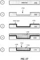
- Various features relate to an integrated device package that includes a bridge in a litho-etchable layer.
- FIG. 1 illustrates an integrated device package 100 that includes a first die 102, a second die 104, and a package substrate 106.
- the package substrate 106 includes a dielectric layer and a plurality of interconnects 110.
- the package substrate 106 is a laminated substrate.
- the plurality of interconnects 110 includes traces, pads and/or vias.
- the first die 102 is coupled to the package substrate 106 through the first set of solder balls 112.
- the second die 104 is coupled to the package substrate 106 through the second set of solder balls 114.
- the package substrate 106 is coupled to a printed circuit board (PCB) 108 through the third set of solder balls 116.
- PCB printed circuit board
- One drawback of the integrated device package 100 shown in FIG. 1 is that it creates an integrated device package with a form factor that may be too large for the needs of mobile computing devices and/or wearable computing devices. This may result in a package that is either too large and/or too thick. That is, the integrated device package configuration shown in FIG. 1 may be too thick and/or have a surface area that is too large to meet the needs and/or requirements of mobile computing devices and/or wearable computing devices.
- Another drawback of the integrated device package 100 is that the configuration of the plurality of interconnects 110 does not provide high density interconnects between the first die 102 and the second die 104. This greatly limits the number of interconnects that can exist between the first die 102 and the second die 104, therefore limiting the communication bandwidth between the first die 102 and the second die 104.
- an integrated device package that includes high density interconnects between dies.
- such an integrated device package will have a better form factor, provide an improved power distribution network (e.g., improved power routing to and from dies), while at the same time meeting the needs and/or requirements of mobile computing devices and/or wearable computing devices.
- Various features relate to an integrated device package that includes a bridge in a litho-etchable layer.
- An example provides an integrated device package base according to claim 1.
- an integrated device package that includes a first die, a second die, and a base (e.g., integrated device package base) coupled to the first die and the second die.
- the base includes an encapsulation portion and a redistribution portion coupled to the encapsulation portion.
- the encapsulation portion is coupled to the first die and the second die.
- the encapsulation portion includes an encapsulation layer, a bridge, and a first via.
- the encapsulation layer may be a litho-etchable material (e.g., material etchable by photolithography process).
- the bridge is at least partially embedded in the encapsulation layer.
- the bridge is configured to provide a first electrical path for a first signal (e.g., input/output signal) between the first die and the second die.
- the first via is in the encapsulation layer.
- the first via is coupled to the bridge.
- the first via and the bridge are configured to provide a second electrical path for a second signal (e.g., power signal, ground reference signal) to the first die.
- the first via has a profile cross section comprising a V shape or a U shape.
- the redistribution portion includes at least one dielectric layer, and at least one interconnect in the at least one dielectric layer.
- the at least one interconnect is coupled to the first via.
- the bridge includes a substrate, a dielectric layer, a first set of interconnects configured to provide the first electrical path for the first signal between the first die and the second die.
- the bridge also includes a through substrate via (TSV) traversing at least the substrate.
- TSV through substrate via
- the TSV is coupled to the first via.
- the TSV is configured to provide the second electrical path for the second signal to the first die.
- the TSV traverses the substrate and the dielectric layer of the bridge.
- An interconnect is an element or component of a device (e.g., integrated device, integrated device package, die) and/or a base (e.g., integrated device package base, package substrate, printed circuit board, interposer) that allows or facilitates an electrical connection between two points, elements and/or components.
- an interconnect may include a trace, a via, a pad, a pillar, a redistribution metal layer, and/or an under bump metallization (UBM) layer.
- UBM under bump metallization
- an interconnect is an electrically conductive material that provides an electrical path for a signal (e.g., data signal, ground signal, power signal).
- An interconnect may include more than one element / component.
- a set of interconnects may include one or more interconnects.
- a redistribution layer or a redistribution metal layer is a metal layer of a redistribution portion of an integrated device, an integrated device package, and/or integrated device package base.
- a redistribution layer may include one or more redistribution interconnects, which are formed on the same metal layer of the redistribution portion.
- a redistribution portion of an integrated device or integrated device package may include several redistribution layers, each redistribution layer may include one or more redistribution interconnects.
- a redistribution portion may include a first redistribution interconnect on a first redistribution layer, and a second redistribution interconnect on a second redistribution layer that is different than the first redistribution layer.
- a litho-patternable layer / material is a material that is photo patternable and developable (e.g., photo etchable). That is, the litho-patternable layer / material is made of a material that can be patterned, developed, etched and/or removed (e.g., through a lithography process) through the exposure of the material to a light source (e.g., ultraviolet (UV) light) through a mask (e.g., photomask).
- a light source e.g., ultraviolet (UV) light
- a mask e.g., photomask
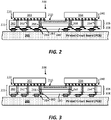
- FIG. 2 illustrates an example of an integrated device package that includes high density die-to-die interconnects.
- FIG. 2 illustrates an example of an integrated device package 200 that includes a base 201, a first die 202, a second die 204, and a bridge 210.
- the bridge 210 may be configured to provide high density die-to-die interconnects.
- the integrated device package 200 may be coupled to a printed circuit board (PCB) 205.
- PCB printed circuit board
- the base 201 may be an integrated device package base.
- the base 201 may be a package substrate.
- the base 201 includes an encapsulation portion 206 and a redistribution portion 208.
- the encapsulation portion 206 is coupled to the redistribution portion 208.
- the encapsulation portion 206 includes an encapsulation layer 260, the bridge 210, and at least one via (e.g., via 266) that is coupled to the bridge 210.
- the bridge 210 is at least partially embedded in the encapsulation layer 260.
- the bridge 210 is configured to provide a first electrical path for a first signal (e.g., input / output signal) between the first die 202 and the second die 204.
- the at least one via and the bridge 210 are configured to provide a second electrical path for a second signal (e.g., power signal) to the first die 202.
- the first die 202 is coupled to the base 201 through a first set of interconnects 220.
- the first set of interconnects 220 may include posts, pillars and/or solder.
- the second die 204 is coupled to the base 201 through a second set of interconnects 240.
- the second set of interconnects 240 may include posts, pillars and/or solder.
- FIG. 2 illustrates that the bridge 210 is located at least partially in the base 201. Specifically, the bridge 210 is at least partially embedded in the encapsulation portion 206. As shown in FIG. 2 , the bridge 210 is at least partially embedded in the encapsulation layer 260.
- the bridge 210 may comprise a silicon bridge, a glass bridge, and/or a ceramic bridge.
- the bridge 210 is configured to provide high density die-to-die interconnects in the integrated device package 200.
- the bridge 210 is configured to provide high density interconnects between the first die 202 and the second die 204 (e.g., high density electrical paths for signals (e.g., input/output signals) between the first die 202 and the second die 204).
- the bridge 210 may be configured to provide at least one first electrical path for at least one first signal between the first die 202 and the second die 204.
- the at least one first electrical path for at least one first signal may include and/or may be defined by several interconnects (e.g., traces, vias) in the bridge 210. Such interconnects that define the at least one first electrical path are further described in detail below in at least FIGS. 4-5 .
- High density interconnects and/or high density electrical paths may refer to any density of wiring or connections per unit area than conventional printed circuit boards and may comprise finer lines and pitch, smaller vias and capture pads, as well as higher connection pad density. High density interconnects may thus be useful to reduce the size, thickness, weight, etc. of the package and/or device as well as enhancing electrical and thermal performance.
- High density interconnects may be defined by interconnects that include a width of about 2 microns ( ⁇ m) or less, a pitch of about 4 microns ( ⁇ m) or less, and/or a spacing of about 2 microns ( ⁇ m) or less.
- the pitch of interconnects may be a center to center distance between two adjacent interconnects.
- the spacing of interconnects may be an edge to edge distance between two adjacent interconnects. Examples of width, pitch and spacing for high density interconnects are further described below in at least FIGS. 4-5 .
- the bridge 210 may include a substrate, a dielectric layer, a set of high density interconnects (e.g., traces, vias), and at least one through substrate via (TSV).
- the substrate may comprise silicon, glass and/or ceramic.
- the substrate, the dielectric layer, the set of high density interconnects (e.g., traces, vias), and the through substrate via (TSV) of the bridge 210 are not numbered or labeled in FIG. 2 .
- a detailed exemplary bridge is illustrated and described below in at least FIGS. 4-5 .
- the first die 202 is coupled to (e.g., in communication with) the second die 204 through at least the bridge 210.
- FIG. 2 illustrates that the first die 202 is coupled to the second die 204 through the first set of interconnects 220, interconnects (e.g., vias, traces) in the bridge 210, and the second set of interconnects 240.
- the first set of interconnects 220, interconnects (e.g., vias, traces) in the bridge 210, and the second set of interconnects 240 provide several high density electrical paths for signals (e.g., input/output signals) between the first die 202 and the second die 204.
- At least one through substrate via is configured to provide at least one electrical path for a power signal and/or a ground reference signal to and/from a die coupled to the bridge 210.
- FIG. 2 illustrates that at least one power signal and/or a ground reference signal can traverse through the bridge 210 to the first die 202 and/or the second die 204.
- the bridge 210 is configured to provide a second electrical path for a second signal (e.g., power signal) to the first die 202.
- an electrical path through the bridge 210 is a more direct path to and from a die, which means a shorter path to and from the die.
- an electrical path through the bridge 210 means that the electrical path does not need to be routed around the bridge, saving space and real estate in the base 201, which can result in an overall smaller form factor for the integrated device package 200.
- a more direct path for the power signal and/or ground reference signal means that less material is used, thereby reducing the cost of fabricating the integrated device package.
- high frequency die-to-die communication through a bridge may require a die-to-die (D2D) buffer (which is not shown).
- the D2D buffer is located in a die coupled to a bridge (e.g., in the die portion that is vertically over the bridge) that is adapted and/or configured to provide die-to-die communication.
- Each die that is coupled to a bridge may include its own respective D2D buffer.
- the D2D buffer may include at least one transistor.
- the D2D buffer may need a power supply (e.g., power signal), and it may be important to have the smallest possible power voltage drop in the signal (e.g., in the power signal) to the D2D buffer (e.g., to a transistor of the D2D buffer). This can be achieved by routing the power signal to the D2D buffer (e.g., D2D of the die) through the bridge.
- a die may have an interconnect to the D2D buffer, that has a metal thickness (e.g., copper thickness) of about 2 microns ( ⁇ m) or less and a lateral length that is greater than 1000 microns ( ⁇ m), which produces a high IR drop in the power signal, where IR is a current resistance.
- a metal thickness e.g., copper thickness
- an interconnect through a bridge to the D2D buffer may have a length of about 100 microns ( ⁇ m) and a metal thickness (e.g., copper thickness) of about 10 microns ( ⁇ m), which provides less voltage drop to the D2D buffer, and thus provides improved die-to-die communication performance.
- a metal thickness e.g., copper thickness
- FIG. 2 shows a high level illustration of a high density interconnect bridge (e.g., bridge 210) that includes at least one TSV configured to provide at least one electrical path for a power signal and/or ground reference signal to and from at least one die.
- a high density interconnect bridge e.g., bridge 210
- FIGS. 4-10 show a high level illustration of a high density interconnect bridge that includes at least one TSV configured to provide at least one electrical path for a power signal and/or ground reference signal to and from at least one die.
- the base 201 includes the encapsulation portion 206 and the redistribution portion 208.
- the base 201 may be an integrated device package base and/or a package substrate of the integrated device package 200.
- the encapsulation portion 206 includes an encapsulation layer 260, a first set of vias 262, a second set of vias 264, a third set of vias 266, and a fourth set of vias 268.
- a set of vias may include one or more vias.
- the encapsulation layer 260 may include one of at least a mold and/or an epoxy fill.
- the encapsulation layer 260 may be a litho-patternable layer (e.g., litho-etchable layer).
- the litho-patternable layer is a material that is photo patternable and developable (e.g., photo etchable).
- the encapsulation layer 260 is made of a material that can be patterned, developed, etched and/or removed through the exposure of the material to a light source (e.g., ultraviolet (UV) light).
- the bridge 210 is at least partially embedded in the encapsulation portion 206 and/or the encapsulation layer 260.
- the encapsulation portion 206 and/or the encapsulation layer 260 at least partially encapsulates the bridge 210.
- the encapsulation layer 260 may be a mold and/or an epoxy fill.
- the encapsulation layer 260 is a layer that includes filler.
- the encapsulation layer 260 may have higher concentration of filler material than a Polyimide (PI) layer and/or a Polybenzoxazole (PBO) layer.
- the first set of vias 262 vertically traverses at least part of the encapsulation layer 260. Thus, the first set of vias 262 is located and/or embedded in the encapsulation layer 260. The first set of vias 262 is coupled to the redistribution portion 208. The first set of vias 262 is also coupled to the first die 202 through the first set of interconnects 220. In some implementations, the encapsulation portion 206 includes a set of pads. The set of pads may be coupled to the first set of vias 262 and the first set of interconnects 220. Examples of pads in an encapsulation portion are further described below in at least FIGS. 6-10 .
- the second set of vias 264 vertically traverses at least part of the encapsulation layer 260.
- the second set of vias 264 is located and/or embedded in the encapsulation layer 260.
- the second set of vias 264 is coupled to the redistribution portion 208.
- the second set of vias 264 is also coupled to the second die 204 through the second set of interconnects 240.
- the encapsulation portion 206 includes a set of pads. The set of pads may be coupled to the second set of vias 264 and the second set of interconnects 240.
- the third set of vias 266 vertically traverses at least part of the encapsulation layer 260.
- the third set of vias 266 is located and/or embedded in the encapsulation layer 260.
- the third set of vias 266 is coupled to the redistribution portion 208.
- the third set of vias 266 is also coupled to the first die 202 through the bridge 210 and the first set of interconnects 220.
- the third set of vias 266 is coupled to the through substrate vias (TSVs) of the bridge 210.
- the encapsulation portion 206 includes a set of pads. The set of pads may be coupled to the bridge 210 and the first set of interconnects 220.
- the third set of vias 266 is configured to provide at least one electrical path for at least one power signal and/or at least one ground reference signal to and from a die (e.g., first die 202), through the bridge 210.
- a via e.g., from the vias 266) and the bridge 210 may be configured to provide a second electrical path for a second signal (e.g., power signal) to the first die 202.
- the fourth set of vias 268 vertically traverses at least part of the encapsulation layer 260.
- the fourth set of vias 268 is coupled to the redistribution portion 208.
- the fourth set of vias 268 is also coupled to the second die 204 through the bridge 210 and the second set of interconnects 240.
- the fourth set of vias 268 is coupled to the through substrate vias (TSVs) of the bridge 210.
- TSVs through substrate vias
- the encapsulation portion 206 includes a set of pads. The set of pads may be coupled to the bridge 210 and the second set of interconnects 240.
- the fourth set of vias 268 is configured to provide at least one electrical path for at least one power signal and/or at least one ground reference signal to and from a die (e.g., second die 204), through the bridge 210.
- the vias in the encapsulation portion 206 are vias that have a width / diameter of about 10 microns ( ⁇ m) or less, and/or a spacing of about 10 microns ( ⁇ m) or less.
- the vias in the encapsulation portion 206 are interconnects that have lower density than the interconnects in the bridge 210.
- at least a majority of the vias in the encapsulation portion 206 have lower density (e.g., greater width, greater spacing) than the interconnects (e.g., traces, vias) in the bridge 210.
- the vias may have different shapes and sizes.
- Various examples of shapes for the vias in the encapsulation layer are further illustrated and described below in at least FIGS. 6-10 .
- the redistribution portion 208 includes a set of dielectric layers 280, and a set of interconnects 282.
- the set of dielectric layers 280 may include one or more dielectric layers.
- the redistribution portion 208 is coupled to a first surface (e.g., bottom surface) of the encapsulation portion 206.
- the set of interconnects 282 may include a trace, a via, a pad, a redistribution interconnect, and/or an under bump metallization (UBM) layer.
- UBM under bump metallization
- the set of interconnects 282 includes redistribution interconnects and UBM layers.
- the set of interconnects 282 is coupled to the first set of vias 262, the second set of vias 264, the third set of vias 266, and the fourth set of vias 268. Some of the set of interconnects 282 may be configured to provide at least one electrical path for at least one power signal and/or at least one ground reference signal. In some implementations, the set of interconnects 282 in the redistribution portion 208 are interconnects that have a width of about 5 microns ( ⁇ m) or less, and/or a spacing of about 5 microns ( ⁇ m) or less. More detailed examples of various redistribution portions are further described in at least FIGS. 6-10 . FIG.
- the set of solder balls 284 is coupled to UBM layers of the set of interconnects 282.
- the set of solder balls 284 is coupled to the PCB 205.
- the integrated device package 200 may also include another encapsulation layer that covers the first die 202 and the second die 204.
- the encapsulation layer may include one of at least a mold and/or an epoxy fill.
- FIG. 3 illustrates another example of an integrated device package that includes high density die-to-die interconnects.
- FIG. 3 illustrates an example of an integrated device package 300 that includes a base 301, the first die 202, the second die 204, and the bridge 210.
- the base 301 may be an integrated device package base and/or a package substrate of the integrated device package 300.
- the base 301 includes the encapsulation portion 206 and a redistribution portion 308.
- the integrated device package 300 is coupled to the printed circuit board (PCB) 205.
- PCB printed circuit board
- the integrated device package 300 is similar to the integrated device package 200, except that in some implementations, the redistribution portion 308 includes a different configuration of interconnects.
- the first die 202 is coupled to the base 201 through the first set of interconnects 220.
- the first set of interconnects 220 may include posts, pillars and/or solder.
- the second die 204 is coupled to the base 201 through the second set of interconnects 240.
- the second set of interconnects 240 may include posts, pillars and/or solder.
- the redistribution portion 308 is coupled to the encapsulation portion 206.
- the redistribution portion 308 includes a set of dielectric layers 280, and a set of interconnects 382.
- the set of dielectric layers 280 may include one or more dielectric layers.
- the redistribution portion 308 is coupled to a first surface (e.g., bottom surface) of the encapsulation portion 206.
- the set of interconnects 382 may include a trace, a via, a pad, a redistribution interconnect, and/or an under bump metallization (UBM) layer.
- UBM under bump metallization
- the set of interconnects 382 includes pads, vias, traces, and UBM layers.
- the set of interconnects 382 is coupled to the first set of vias 262, the second set of vias 264, the third set of vias 266, and the fourth set of vias 268.
- Some of the set of interconnects 382 may be configured to provide at least one electrical path for at least one power signal and/or at least one ground reference signal.
- the set of interconnects 382 in the redistribution portion 308 are interconnects that have a width of about 5 microns ( ⁇ m) or less, and/or a spacing of about 5 microns ( ⁇ m) or less. More detailed examples of various redistribution portions are further described in at least FIGS.
- FIG. 3 illustrates the set of solder balls 284 is coupled to the set of interconnects 382.
- the set of solder balls 284 is coupled to UBM layers of the set of interconnects 382.
- the set of solder balls 284 is coupled to the PCB 205.
- the integrated device package 300 may also include another encapsulation layer that covers the first die 202 and the second die 204.
- the encapsulation layer may include one of at least a mold and/or an epoxy fill.
- an integrated device package may include a bridge (e.g., silicon bridge, glass bridge, ceramic bridge) that is configured to provide high density die-to-die interconnects, and through substrate vias (TSVs) configured to provide at least one electrical path for at least one power signal and/or at least one ground reference signal to and from one or more dies.
- TSVs substrate vias
- FIGS. 4 and 5 illustrate conceptual examples of such bridges configured to provide high density interconnects and TSVs in an integrated device package.
- FIG. 4 illustrates a profile view of an example of the bridge 210 (e.g., silicon bridge).
- the bridge 210 includes a substrate 402, a dielectric layer 404, at least one first interconnect 406, at least one second interconnect 408, at least one third interconnect 410, at least one fourth interconnect 418, and at least one fifth interconnect 420.
- the bridge 210 may be implemented in any of the integrated device package illustrated and described in the present disclosure.
- the bridge 210 may be the bridge of FIGS. 2-3 .
- the bridge 210 is a means (e.g., bridge means) for providing a die-to-die electrical path or die-to-die electrical connection between a first die and a second die.
- the at least one first interconnect 406, the at least one second interconnect 408, and the at least on third interconnect 410 may define at least one first electrical path for at least one first signal between a first die and a second die.
- the at least one first interconnect 406, the at least one second interconnect 408, and the at least on third interconnect 410 may form at least one first set of interconnects that is configured to provide at least one first electrical path for at least one first signal between a first die and a second die.
- the bridge 210 is a means (e.g., bridge means) for providing at least one second electrical path for at least a power signal and/or at least a ground reference signal to and from a first die. In some implementations, the bridge 210 is a means (e.g., bridge means) for providing at least one third electrical path for at least a power signal and/or at least a ground reference signal to and from a second die.
- the means e.g., bridge means
- the substrate 402 comprises a silicon substrate, a glass substrate, and/or a ceramic substrate.
- the first interconnect 406 may be at least one trace located on the substrate 402.
- the dielectric layer 404 covers the first interconnect 406 and the substrate 402.
- the second and third interconnects 408 and 410 are vias that vertically traverses the dielectric layer 404.
- the second and third interconnects 408 and 410 are coupled to the first interconnect 406.
- the first, second, and third interconnects 406, 408 and 410 are high density interconnects.
- high density interconnects are interconnects that have a width of about 2 microns ( ⁇ m) or less, and/or a spacing of about 2 microns ( ⁇ m) or less.
- the width of an interconnect may be the width of the trace and/or line.
- the width of an interconnect may be the diameter of a via and/or a pad.
- a spacing is an edge to edge distance between two neighboring / adjacent interconnects.
- the fourth interconnect 418 may be a via that traverses the substrate 402 and the dielectric layer 404.
- the fourth interconnect 418 may be a through substrate via (TSV) that traverses the substrate 402 and the dielectric layer 404.
- TSV through substrate via
- the fourth interconnect 418 may be a combination of two or more vias (e.g., first via in the substrate 402 and a second via in the dielectric layer 404).
- the fourth interconnect 418 is configured to provide at least one electrical path (e.g., second electrical path) for at least one second signal (e.g., at least one power signal and/or at least one ground reference signal) to and from a die (e.g., first die).
- the fifth interconnect 420 may be a via that traverses the substrate 402 and the dielectric layer 404.
- the fifth interconnect 420 may be a through substrate via (TSV) that traverses the substrate 402 and the dielectric layer 404.
- TSV through substrate via
- the fifth interconnect 420 may be a combination of two or more vias (e.g., first via in the substrate 402 and a second via in the dielectric layer 404).
- the fifth interconnect 420 is configured to provide at least one electrical path (e.g., third electrical path) for at least one third signal (e.g., at least one power signal and/or at least one ground reference signal) to and from a die (e.g., second die).
- the fourth and fifth interconnects 418 and 420 are high density interconnects.
- the bridge 210 may include several first interconnects, second interconnects, third interconnects, fourth interconnects, and fifth interconnects.
- FIG. 5 illustrates a plan view (e.g., top view) of an example of the bridge 210 (e.g., silicon bridge) that includes a substrate (not visible), the dielectric layer 404, the first interconnect 406, the second interconnect 408, the third interconnect 410, the fourth interconnect 418, and the fifth interconnect 420.
- FIG. 5 illustrates the width and spacing of interconnects. The width of an interconnect is illustrated by (W), and the spacing between two neighboring / adjacent interconnects is illustrated by (S).
- the first interconnect 406, the second interconnect 408, the third interconnect 410, the fourth interconnect 418, and/or the fifth interconnect 420 are high density interconnects.
- high density interconnects are interconnects that have a width of about 2 microns ( ⁇ m) or less, and/or a spacing of about 2 microns ( ⁇ m) or less.
- an electrical path through the bridge 210 is a more direct path to and from a die, which means a shorter path to and from the die.
- an electrical path through the bridge 210 means that the electrical path does not need to be routed around the bridge, saving space and real estate in the base 201, which can result in an overall smaller form factor for the integrated device package 200.
- a more direct path for the power signal and/or ground reference signal means that less material is used, thereby reducing the cost of fabricating the integrated device package.
- TSVs may help provide improved performance in die-to-die communication.
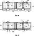
- FIG. 6 illustrates an example of a portion of integrated device package base 600 of an integrated device package.
- the integrated device package base 600 may correspond to at least the encapsulation portion 206 and the redistribution portion 208 of FIG. 2 .
- the integrated device package base 600 is a package substrate of an integrated device package.
- the integrated device package base 600 includes an encapsulation portion 602 and a redistribution portion 604.
- the encapsulation portion 602 includes an encapsulation layer 606, a first via 603, a second via 605, a first pad 611, a second pad 613, a third pad 615, a solder resist layer 608, and the bridge 210.
- the encapsulation layer 606 is a litho-patternable material (e.g., litho-etchable material) that is photo patternable and developable (e.g., photo etchable).
- the encapsulation layer 606 is made of a material that can be patterned, develop, etched and/or removed through the exposure of the material to a light source (e.g., ultraviolet (UV) light).
- the encapsulation layer 606 may include one of at least a mold and/or an epoxy fill.
- the first via 603 vertically traverses the encapsulation layer 606.
- the first pad 611 is coupled to the first via 603.
- the second via 605 vertically traverses the encapsulation layer 606.
- the second via 605 is located and/or embedded in the encapsulation layer 606.
- the second via 605 is coupled to the interconnect 418 of the bridge 210.
- the interconnect 418 may be a through substrate via (TSVs) of the bridge 210.
- TSVs through substrate via
- the second via 605, the interconnect 418, and the second pad 613 are configured to provide an electrical path (e.g., second electrical path) for a second signal (e.g., a power signal and/or a ground reference signal) to and from a die (e.g., first die 202).
- a second signal e.g., a power signal and/or a ground reference signal
- the solder resist layer 608 covers a first surface (e.g., top surface) of the encapsulation layer 606.
- a solder ball may be coupled to the pads 611, 613, and/or 615.
- the via 603 is part of a set of vias in the encapsulation layer 606, where the set of vias has a first density (e.g., first width and/or first spacing).
- FIG. 6 also illustrates that the bridge 210 is at least partially embedded in the encapsulation layer 606 of the encapsulation portion 602.
- the bridge 210 is configured to provide high density electrical paths (e.g., high density die-to-die interconnects) in the encapsulation portion 602.
- the bridge 210 is also configured to provide an electrical path for a signal (e.g., power signal) to a die through the substrate 402 of the bridge 210.
- a signal e.g., power signal
- the redistribution portion 604 is coupled to the encapsulation portion 602.
- the redistribution portion 604 includes a first dielectric layer 642, a second dielectric layer 644, and a third dielectric layer 648, an interconnect 643, and an interconnect 653.
- the first, second, and/or third dielectric layers 642, 644, and/or 648 may be collectively a single dielectric layer.
- the interconnects 643 and 653 may be redistribution interconnects comprising a diagonal portion and a horizontal portion.
- the interconnects 643 and 653 are U or V shaped redistribution interconnects.
- the interconnects 643 and 653 may be configured to couple to solder balls (e.g., printed circuit board side solder balls).
- the interconnect 643 of the redistribution portion 604 is coupled to the via 603 of the encapsulation portion 602.
- the interconnect 653 of the redistribution portion 604 is coupled to the second via 605 in the encapsulation portion 602.
- the interconnect 653, the second via 605, the interconnect 418, and the second pad 613 are configured to provide an electrical path for a power signal and/or a ground reference signal to and from a die (e.g., first die 202).
- a first die (e.g., die 202) may be electrically coupled to a second die (e.g., second die 204) through the third pad 615, the interconnect 410, and the interconnect 406.
- the third pad 615, the interconnect 410, and the interconnect 406 define an electrical path for die-to-die connection between the first and second dies (e.g., dies 202 and 204).
- FIG. 7 illustrates another example of a portion of integrated device package base 700 of an integrated device package.
- the integrated device package base 700 may correspond to at least the encapsulation portion 206 and the redistribution portion 308 of FIG. 3 .
- the integrated device package base 700 is a package substrate of an integrated device package.
- the integrated device package base 700 includes an encapsulation portion 602 and a redistribution portion 704.
- the encapsulation portion 602 includes an encapsulation layer 606, a first via 603, a second via 605, a first pad 611, a second pad 613, a third pad 615, a solder resist layer 608, and the bridge 210.
- the encapsulation layer 606 is a litho-patternable material (e.g., litho-etchable material) that is photo patternable and developable (e.g., photo etchable).
- the encapsulation layer 606 is made of a material that can be patterned, develop, etched and/or removed through the exposure of the material to a light source (e.g., ultraviolet (UV) light).
- the encapsulation layer 606 may include one of at least a mold and/or an epoxy fill.
- the first via 603 vertically traverses the encapsulation layer 606.
- the first pad 611 is coupled to the first via 603.
- the second via 605 vertically traverses the encapsulation layer 606.
- the second via 605 is coupled to the interconnect 418 of the bridge 210.
- the interconnect 418 may be a through substrate via (TSVs) of the bridge 210.
- the second pad 613 is coupled to the interconnect 418.
- the second via 605, the interconnect 418, and the second pad 613 are configured to provide an electrical path for a power signal and/or a ground reference signal to and from a die (e.g., first die 202).
- the solder resist layer 608 covers a first surface (e.g., top surface) of the encapsulation layer 606.
- a solder ball may be coupled to the pads 611, 613, and/or 615.
- the via 603 is part of a set of vias in the encapsulation layer 606, where the set of vias has a first density (e.g., first width and/or first spacing).
- FIG. 7 also illustrates that the bridge 210 is at least partially embedded in the encapsulation layer 606 of the encapsulation portion 602.
- the bridge 210 is configured to provide high density electrical paths (e.g., high density die-to-die interconnects) in the encapsulation portion 602.
- the bridge 210 is also configured to provide an electrical path for a signal (e.g., power signal) to a die through the substrate 402 of the bridge 210.
- a signal e.g., power signal
- the redistribution portion 704 is coupled to the encapsulation portion 602.
- the redistribution portion 704 includes a first dielectric layer 642, a second dielectric layer 644, and a third dielectric layer 648, an interconnect 743, an interconnect 745, an interconnect 753, and an interconnect 755.
- the first, second, and/or third dielectric layers 642, 644, and/or 648 may be collectively a single dielectric layer.
- the interconnects 743 and 753 may be vias.
- the interconnects 745 and 755 may be traces and/or pads. In some implementations, the interconnects 745 and 755 may be configured to couple to solder balls (e.g., printed circuit board side solder balls).
- the interconnect 745 is coupled to the interconnect 743.
- the interconnect 743 of the redistribution portion 704 is coupled to the via 603 of the encapsulation portion 602.
- the interconnect 755 is coupled to the interconnect 753.
- the interconnect 753 of the redistribution portion 704 is coupled to the second via 605 in the encapsulation portion 602.
- the interconnect 755, the interconnect 753, the second via 605, the interconnect 418, and the second pad 613 are configured to provide an electrical path for a power signal and/or a ground reference signal to and from a die (e.g., first die 202).
- a first die (e.g., die 202) may be electrically coupled to a second die (e.g., second die 204) through the third pad 615, the interconnect 410, and the interconnect 406.
- the third pad 615, the interconnect 410, and the interconnect 406 define an electrical path for die-to-die connection between the first and second dies (e.g., dies 202 and 204).
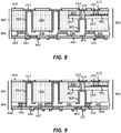
- FIGS. 6-7 illustrate vias (e.g., via 603, via 605) in an encapsulation layer comprising a certain shapes. As shown in FIGS. 6-7 the vias in the encapsulation layer 606 are formed by filling cavities in the encapsulation layer 606. However, in some implementations, the vias in an encapsulation layer may have a different shape and/or configuration.
- FIGS. 8-9 illustrate vias in an encapsulation layer comprising different shapes.
- the vias in the encapsulation layer are formed by conform fill, where one or more metal layers are formed on the walls of the cavities leaving another cavity that is filled with a dielectric layer.
- the vias have a bowl or can-like shape.
- FIG. 8 illustrates an example of a portion of integrated device package base 800 of an integrated device package.
- the integrated device package base 800 may correspond to at least the encapsulation portion 206 and the redistribution portion 208 of FIG. 2 .
- the integrated device package base 800 is a package substrate of an integrated device package.
- the integrated device package base 800 includes an encapsulation portion 802 and a redistribution portion 804.
- the encapsulation portion 802 includes an encapsulation layer 606, a first via 803, a second via 805, a first pad 611, a second pad 613, a third pad 615, a solder resist layer 608, and the bridge 210.
- the encapsulation layer 606 is a litho-patternable material (e.g., litho-etchable material) that is photo patternable and developable (e.g., photo etchable).
- the encapsulation layer 606 is made of a material that can be patterned, develop, etched and/or removed through the exposure of the material to a light source (e.g., ultraviolet (UV) light).
- the encapsulation layer 606 may include one of at least a mold and/or an epoxy fill.
- the first via 803 includes a V shape profile cross section or a U shape profile cross section.
- the first via 803 may be a conform fill via that forms the shape of the cavity in which it is formed.
- the first via 803 is formed along at least the walls of the cavity in which it is formed.
- the first via 803 also includes a wing portion that is formed in the redistribution portion 804.
- the wing portion of the first via 803 traverses laterally in the redistribution portion 804.
- the wing portion may be referred to as a wing interconnect of the via.
- the first via 803 vertically traverses the encapsulation layer 606.
- the first pad 611 is coupled to the first via 803.
- the second via 805 also includes a V shape profile cross section or a U shape profile cross section.
- the second via 805 may be a conform fill via that forms the shape of the cavity in which it is formed.
- the second via 805 is formed along at least the walls of the cavity in which it is formed.
- the second via 805 also includes a wing portion that is formed in the redistribution portion 804. The wing portion of the second via 805 traverses laterally in the redistribution portion 804.
- a dielectric layer 840 is located within the cavity created by the vias (e.g., via 803, via 805) of the encapsulation layer 606.
- the second via 805 vertically traverses the encapsulation layer 606.
- the second via 805 is at least partially located and/or at least partially embedded in the encapsulation layer 606.
- the second via 805 is coupled to the interconnect 418 of the bridge 210.
- the interconnect 418 may be a through substrate via (TSVs) of the bridge 210.
- TSVs through substrate via
- the second pad 613 is coupled to the interconnect 418.
- the second via 805, the interconnect 418, and the second pad 613 are configured to provide an electrical path for a power signal and/or a ground reference signal to and from a die (e.g., first die 202).
- the solder resist layer 608 covers a first surface (e.g., top surface) of the encapsulation layer 606.
- a solder ball may be coupled to the pads 611, 613, and/or 615.
- the via 803 is part of a set of vias in the encapsulation layer 606, where the set of vias has a first density (e.g., first width and/or first spacing).
- FIG. 8 also illustrates that the bridge 210 is at least partially embedded in the encapsulation layer 606 of the encapsulation portion 802.
- the bridge 210 is configured to provide high density electrical paths (e.g., high density die-to-die interconnects) in the encapsulation portion 802.
- the bridge is also configured to provide an electrical path for a signal (e.g., power signal) to a die through the substrate 402 of the bridge 210.
- a signal e.g., power signal
- the redistribution portion 804 is coupled to the encapsulation portion 802.
- the redistribution portion 804 includes dielectric layer 840, a dielectric layer 844, and a dielectric layer 848, an interconnect 843, and an interconnect 853.
- the dielectric layers 840, 844, and/or 848 may be collectively a single dielectric layer.
- the interconnects 843 and 853 may be redistribution interconnects comprising a diagonal portion and a horizontal portion.
- the interconnects 843 and 853 include U or V shaped redistribution interconnects.
- the interconnects 843 and 853 may be configured to couple to solder balls (e.g., printed circuit board side solder balls).
- the interconnect 843 of the redistribution portion 804 is coupled to the via 803 of the encapsulation portion 802 (e.g., coupled to wing portion of the first via 803).
- the interconnect 853 of the redistribution portion 804 is coupled to the second via 805 (e.g., coupled to wing portion of the second via 805) in the encapsulation portion 802.
- the interconnect 853, the second via 805, the interconnect 418, and the second pad 613 are configured to provide an electrical path for a power signal and/or a ground reference signal to and from a die (e.g., first die 202).
- FIG. 8 illustrates that the redistribution portion 804 may also include a first under bump metallization (UBM) layer 845 and a second under bump metallization (UBM) layer 855.
- the first UBM layer 845 is coupled to the interconnect 843.
- the second UBM layer 855 is coupled to the interconnect 853.
- the first UBM layer 845 and the second UBM layer 855 are configured to couple to solder balls.
- a first die (e.g., die 202) may be electrically coupled to a second die (e.g., second die 204) through the third pad 615, the interconnect 410, and the interconnect 406.
- the third pad 615, the interconnect 410, and the interconnect 406 define an electrical path for die-to-die connection between the first and second dies (e.g., dies 202 and 204).
- FIG. 9 illustrates another example of a portion of integrated device package base 900 of an integrated device package.
- the integrated device package base 900 may correspond to at least the encapsulation portion 206 and the redistribution portion 308 of FIG. 3 .
- the integrated device package base 900 is a package substrate of an integrated device package.
- the integrated device package base 900 includes an encapsulation portion 802 and a redistribution portion 904.
- the encapsulation portion 802 includes an encapsulation layer 606, a first via 803, a second via 805, a first pad 611, a second pad 613, a third pad 615, a solder resist layer 608, and the bridge 210.
- the encapsulation layer 606 is a litho-patternable material (e.g., litho-etchable material) that is photo patternable and developable (e.g., photo etchable).
- the encapsulation layer 606 is made of a material that can be patterned, develop, etched and/or removed through the exposure of the material to a light source (e.g., ultraviolet (UV) light).
- the encapsulation layer 606 may include one of at least a mold and/or an epoxy fill.
- the first via 803 includes a V shape profile cross section or a U shape profile cross section.
- the first via 803 may be a conform fill via that forms the shape of the cavity in which it is formed.
- the first via 803 is formed along at least the walls of the cavity in which it is formed.
- the first via 803 also includes a wing portion that is formed in the redistribution portion 904.
- the wing portion of the first via 803 traverses laterally in the redistribution portion 904.
- the wing portion may be referred to as a wing interconnect of the via.
- the first via 803 vertically traverses the encapsulation layer 606.
- the first pad 611 is coupled to the first via 803.
- the second via 805 also includes a V shape profile cross section or a U shape profile cross section.
- the second via 805 may be a conform fill via that forms the shape of the cavity in which it is formed.
- the second via 805 is formed along at least the walls of the cavity in which it is formed.
- the second via 805 also includes a wing portion that is formed in the redistribution portion 904. The wing portion of the second via 805 traverses laterally in the redistribution portion 904.
- a dielectric layer 840 is located within the cavity created by the vias (e.g., via 803, via 805) of the encapsulation layer 606.
- the second via 805 vertically traverses the encapsulation layer 606.
- the second via 805 is coupled to the interconnect 418 of the bridge 210.
- the interconnect 418 may be a through substrate via (TSVs) of the bridge 210.
- TSVs through substrate via
- the second pad 613 is coupled to the interconnect 418.
- the second via 805, the interconnect 418, and the second pad 613 are configured to provide an electrical path for a power signal and/or a ground reference signal to and from a die (e.g., first die 202).
- the solder resist layer 608 covers a first surface (e.g., top surface) of the encapsulation layer 606.
- a solder ball may be coupled to the pads 611, 613, and/or 615.
- the via 803 is part of a set of vias in the encapsulation layer 606, where the set of vias has a first density (e.g., first width and/or first spacing).
- FIG. 9 also illustrates that the bridge 210 is at least partially embedded in the encapsulation layer 606 of the encapsulation portion 802.
- the bridge 210 is configured to provide high density electrical paths (e.g., high density die-to-die interconnects) in the encapsulation portion 802.
- the bridge is also configured to provide an electrical path for a signal (e.g., power signal) to a die through the substrate 402 of the bridge 210.
- a signal e.g., power signal
- the redistribution portion 904 is coupled to the encapsulation portion 802.
- the redistribution portion 904 includes a dielectric layer 840, a dielectric layer 844, and a dielectric layer 848, an interconnect 943, an interconnect 945, an interconnect 953, and an interconnect 955.
- the dielectric layers 842, 844, and/or 848 may be collectively a single dielectric layer.
- the interconnects 943 and 953 may be vias.
- the interconnects 945 and 955 may be traces and/or pads. In some implementations, the interconnects 945 and 955 may be configured to couple to solder balls (e.g., printed circuit board side solder balls).
- the interconnect 945 is coupled to the interconnect 943.
- the interconnect 943 of the redistribution portion 904 is coupled to the via 803 of the encapsulation portion 802 (e.g., coupled to the wing portion of the first via 803).
- the interconnect 955 is coupled to the interconnect 953.
- the interconnect 953 of the redistribution portion 904 is coupled to the second via 805 in the encapsulation portion 802 (e.g., coupled to the wing portion of the second via 805).
- the interconnect 955, the interconnect 953, the second via 805, the interconnect 418, and the second pad 613 are configured to provide an electrical path for a power signal and/or a ground reference signal to and from a die (e.g., first die 202).
- FIG. 9 illustrates that the redistribution portion 904 may also include a first under bump metallization (UBM) layer 947 and a second under bump metallization (UBM) layer 957.
- the first UBM layer 947 is coupled to the interconnect 945.
- the second UBM layer 957 is coupled to the interconnect 955.
- the first UBM layer 947 and the second UBM layer 957 are configured to couple to solder balls.
- a first die (e.g., die 202) may be electrically coupled to a second die (e.g., second die 204) through the third pad 615, the interconnect 410, and the interconnect 406.
- the third pad 615, the interconnect 410, and the interconnect 406 define an electrical path for die-to-die connection between the first and second dies (e.g., dies 202 and 204).
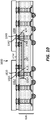
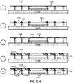
- FIG. 10 illustrates an example of an integrated device package 1000 that includes two dies coupled to an integrated device package base.
- the integrated device package 1000 includes a first die 1002 and a second die 1004, and the base 600.
- the first die 1002 and the second die 1004 are coupled to the base 600.
- the first die 1002 and the second die 1004 may be coupled to any of the integrated device package bases (e.g., base 201, base 301, base 700, base 800, base 900) described in the present disclosure.
- the first die 1002 includes an under bump metallization (UBM) layer 1020 (optional), a pillar 1022, and solder 1024.
- UBM under bump metallization
- the first die 1002 is coupled to the integrated device package base 600 through the UBM layer 1020 (optional), the pillar 1022, the solder 1024, and the pad 613 of the integrated device package base 600.
- the second die 1004 includes an under bump metallization (UBM) layer 1040 (optional), a pillar 1042, and solder 1044.
- UBM under bump metallization
- the second die 1004 is coupled to the integrated device package base 600 through the UBM layer 1040 (optional), the pillar 1042, the solder 1044, and the pad 623 of the integrated device package base 600.
- a fill 1050 is located between the first die 1002 and the integrated device package base 600.
- the fill 1050 may include at least a non-conducting fill (NCF) and/or a non-conducting paste (NCP).
- the fill 1050 covers the interconnects (e.g., pillar 1022, solder 1024, pad 613) between the first die 1002 and the integrated device package base 600.
- the fill 1050 is also located between the second die 1004 and the integrated device package base 600.
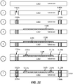
- providing / fabricating a high density interconnect bridge with through substrate vias includes several processes.
- FIG. 11 illustrates an exemplary sequence for providing / fabricating a high density interconnect bridge that includes TSVs.
- the sequence of FIG. 11 may be used to provide / fabricate the bridge of FIGS. 2-10 and/or other bridges described in the present disclosure. However, for the purpose of simplification, FIG. 11 will be described in the context of providing / fabricating the bridge of FIG. 4 .
- FIG. 11 may combine one or more stages in order to simplify and/or clarify the sequence for providing / fabricating a bridge.
- the order of the processes may be changed or modified.
- Stage 1 of FIG. 11 illustrates a state after a substrate 1102 is provided.
- the substrate 1102 is provided by a supplier.
- the substrate 1102 is fabricated (e.g., formed).
- the substrate 1102 comprises a silicon substrate, a glass substrate, a ceramic substrate, and/or wafer (e.g., silicon wafer).
- Stage 2 illustrates a state after cavities 1103 (e.g., cavity 1103a, cavity 1103b) are formed in the substrate 1102. Different implementations may form the cavities 1103 differently. In some implementations, a laser and/or a lithography process is used to form the cavities 1103.
- cavities 1103 e.g., cavity 1103a, cavity 1103b
- Stage 3 illustrates a state after vias 1104 (e.g., via 1104a, via 1104b) are formed in the cavities of the substrate 1102.
- the vias 1104 may be through substrate vias (TSVs).
- TSVs substrate vias
- Different implementations may form the vias 1104 differently. For example, a plating process and/or a pasting process may be use to form the vias 1104.
- Stage 4 illustrates a state after a metal layer 1106 is formed on the substrate 1102.
- the metal layer 1106 may form and/or define one or more high density interconnects (e.g., as described in FIGS. 4-5 ). These high density interconnects may be high density electrical paths between dies.
- providing the metal layer 1106 includes forming (e.g., plating) one or more metal layers (e.g., seed layer and metal layer) and selectively etching portions of the one or more metal layers.
- FIGS. 15-18 illustrate examples of forming one or more metal layers using several plating processes.
- Stage 5 illustrates a state after a dielectric layer 1108 is formed over the substrate 1102 and the metal layer 1106. Different implementations may use different materials for the dielectric layer 1108.
- Stage 6 illustrates a state after the cavities 1109 (e.g., cavity 1109a, cavity 1109b) and the cavities 1111 (e.g., cavity 1111a, cavity 1111b) are formed in the dielectric layer 1108.
- Different implementations may use different processes for forming cavities in the dielectric layer 1108.
- a laser may be used to form the cavities.
- a photo etching process is used to form the cavities.
- Stage 7 illustrates a state after the vias 1112 (e.g., via 1112a, via 1112b) and the vias 1114 (e.g., via 1114a, via 1114b) are formed in the dielectric layer 1108.
- the vias 1112 are formed in the cavities 1109 of the dielectric layer 1108, and the vias 1114 are formed in the cavities 1111 of the dielectric layer 1108.
- the vias 1112 and the vias 1104 in combination form a through substrate vias (TSVs) that vertically traverses the entire bridge 1130.
- TSVs through substrate vias
- the vias 1112 are metal layer(s) that are formed using one or more plating processes.
- the vias 1114 are coupled to the metal layer 1106.
- FIGS. 15-18 illustrate examples of forming one or more metal layers using several plating processes.
- stage 7 illustrates a bridge 1130 (e.g., silicon bridge) that may be implemented in an encapsulation layer of any of the base described in the present disclosure. It is noted that in some implementations, the vias 1104 and/or 1112 may be formed once the bridge is positioned or embedded in an encapsulation layer of the base.
- FIG. 12 illustrates an exemplary flow diagram of a method 1200 for providing / fabricating a high density interconnect silicon bridge.
- the method of FIG. 12 may be used to provide / fabricate the high density interconnect silicon bridge of FIGS. 2-10 and/or other high density interconnect silicon bridge in the present disclosure.
- FIG. 12 may combine one or more processes in order to simplify and/or clarify the method for providing a passive device package.
- the order of the processes may be changed or modified.
- the method provides (at 1205) a substrate.
- providing the substrate may include receiving a substrate from a supplier or fabricating (e.g., forming) a substrate.
- the substrate comprises a silicon substrate, a glass substrate, a ceramic substrate and/or wafer (e.g., silicon wafer).
- the method forms (at 1210) a through substrate via (TSV) in the substrate.
- TSV through substrate via
- forming a TSV includes forming a cavity in the substrate and filling the cavity with an electrically conductive material to define the TSV.
- a laser may be used to form the cavities.
- a photo etching process is used to form the cavities.
- a plating process or screen printing process may be used to form the vias.
- the TSV is configured to provide an electrical path for a power signal or a ground reference signal.
- the method forms (at 1215) a metal layer on the substrate to form one or more high density interconnect (e.g., as described in FIGS. 4-5 ).
- forming the metal layer includes forming (e.g., plating) one or more metal layers (e.g., seed layer and metal layer) and selectively etching portions of the one or more metal layers.
- FIGS. 15-18 illustrate examples of providing one or more metal layers using several plating processes.
- the method forms (at 1220) a dielectric layer over the substrate and the metal layer.
- Different implementations may use different materials for the dielectric layer.
- the method then forms (at 1225) at least one cavity in the dielectric layer.
- Different implementations may use different processes for forming cavities in the dielectric layer.
- a laser may be used to form the cavities.
- a photo etching process is used to form the cavities.
- the method optionally forms (at 1230) a via in the dielectric layer. Specifically, the method fills the cavity of the dielectric layer with one or more conducting material (e.g., metal layers) to form a via in the cavity.
- One or more of the vias may be formed over the TSVs in the substrate.
- the vias are high density vias (e.g., as described in FIGS. 4-5 ).
- the vias are metal layer(s) that are formed using one or more plating processes.
- FIGS. 15-18 illustrate examples of providing one or more metal layers using several plating processes. It should be noted that in some implementations, the vias may be formed once the bridge is positioned or embedded in a photo patternable layer of the base portion.
- FIG. 13 (which includes FIGS. 13A-13C ) illustrates an exemplary sequence for providing / fabricating an integrated device package that includes a high density interconnect bridge that includes a through substrate via, in an encapsulation layer.
- the sequence of FIGS. 13A-13C may be used to provide / fabricate the integrated device package of FIGS. 2-3 , 6-10 and/or other integrated device packages in the present disclosure.
- FIGS. 13A-13C will be described in the context of fabricating the integrated device package of FIG. 3 .
- FIGS. 13A-13C may combine one or more stages in order to simplify and/or clarify the sequence for providing an integrated device package.
- the order of the processes may be changed or modified.
- Stage 1 of FIG. 13A illustrates a state after a bridge 1302 is provided (e.g., mounted) on a carrier 1300.
- the carrier 1300 is provided by a supplier.
- the carrier 1300 is fabricated (e.g., formed).
- the carrier 1300 comprises a silicon substrate and/or wafer (e.g., silicon wafer).
- the bridge 1302 may include a substrate, at least one metal layer, at least one via, at least one dielectric layer, and/or at least one through substrate via (TSV), as described in at least FIGS. 2-3 . Examples of the bridge 1302 include the bridge shown and described in FIGS. 4-5 .
- the bridge 1302 is a high density interconnect bridge configured to provide a connection and/or electrical path for signals between two dies, and to provide a connection and/or electrical path to and from a die for a power signal and/or a ground reference signal. As shown at stage 1, the bridge 1302 is coupled to a surface of the carrier 1300. In some implementations, an adhesive is used to mechanically couple the bridge 1302 to the carrier 1300.
- Stage 2 illustrates a state after an encapsulation layer 1304 is provided (e.g., formed) on the carrier 1300 and the bridge 1302.
- the encapsulation layer 1304 may be a litho-etchable dielectric layer (e.g., etchable by using a photo etching process).
- the encapsulation layer 1304 at least partially encapsulates or at least partially covers the bridge 1302.
- the encapsulation layer 1304 may comprise a mold and/or an epoxy fill.
- Stage 3 illustrates a state after at least one cavity 1305 is formed in the encapsulation layer 1304.
- the at least one cavity 1305 is removed by using a photo etching process that selectively removes portions of the encapsulation layer 1304 by selectively exposing the encapsulation layer 1304 to a light source (e.g., UV light).
- a light source e.g., UV light
- Stage 4 illustrates a state after at least one via 1306 (e.g., via 1306a, via 1306b) is formed in the encapsulation layer 1304.
- the via 1306b and the via 1306b are formed in the cavities of the encapsulation layer 1304.
- the via 1306a traverses the encapsulation layer 1304.
- the via 1306b is formed in the encapsulation layer 1304 to couple to the bridge 1302.
- the via 1306 is metal layer(s) that are formed using one or more plating processes.
- FIGS. 15-18 illustrate examples of forming one or more metal layers using several plating processes.
- Stage 5 illustrates a state after a first metal layer 1308 is formed on a first surface of the encapsulation layer 1304 and/or vias 1306.
- the first metal layer 1308 may be configured to define one or more pads (e.g., pad 1308a, pad 1308b) and/or traces on the encapsulation layer 1304.
- the pad 1308a is formed over the via 1306a.
- the pad 1308b is formed over the via 1306b.
- providing the first metal layer 1308 includes forming (e.g., plating) one or more metal layers (e.g., seed layer and metal layer) and selectively etching portions of the one or more metal layers.
- FIGS. 15-18 illustrate examples of providing one or more metal layers using several plating processes.
- the via 1306 and the first metal layer 1308 may be formed at the same time.
- the via 1306 is a conform via that is formed along the walls of the cavity as described in FIGS. 8-9 .
- the via 1306 (e.g., via 1306a, via 1306b) may have a profile cross section that includes a V shape or a U shape.
- Stage 6 illustrates a state after a first dielectric layer 1310 is provided (e.g., formed) on the encapsulation layer 1304 and the first metal layer 1308, and after a cavity 1312 is formed in the first dielectric layer 1310.
- the cavity 1312 may be formed through a photo etching process.
- Stage 7 illustrates a state after at least one via 1314 is formed in the first dielectric layer 1310 and a metal layer 1316 is formed on the first dielectric layer 1310.
- the via 1314 and the metal layer 1316 are formed by forming (e.g., plating) one or more metal layers (e.g., seed layer and metal layer) and selectively etching portions of the one or more metal layers.
- FIGS. 15-18 illustrate examples of providing one or more metal layers using several plating processes.
- the metal layer 1316 may be an interconnect in a redistribution portion.
- Stage 8 illustrates a state after a second dielectric layer 1318 is provided (e.g., formed) on the first dielectric layer 1310 and the metal layer 1316.
- Stage 9 illustrates a state after an under bump metallization (UBM) layer 1320 is formed on the second dielectric layer 1318.
- the UBM layer 1320 is formed such that the UBM layer 1320 is coupled to the metal layer 1316.
- providing the UBM layer 1320 includes forming (e.g., plating) one or more metal layers (e.g., seed layer and metal layer) and selectively etching portions of the one or more metal layers.
- FIGS. 15-18 illustrate examples of forming one or more metal layers using several plating processes.
- Stage 10 illustrates a state after the carrier 1300 is decoupled from base 1330, which includes the bridge 1302, the encapsulation layer 1304, the via 1306, the metal layer 1308, the dielectric layer 1310, the via 1314, the metal layer 1316, the dielectric layer 1318, and the UBM layer 1320.
- Stage 11 illustrates a state after the base 1330 is optionally flipped.
- Stage 12 illustrates a state after a metal layer 1340 is formed on the encapsulation layer 1304 and the bridge 1302.
- the metal layer 1340 may form one or more pads and/or traces. Some portions of the metal layer 1340 may be coupled to vias in the encapsulation layer 1304 and vias in the bridge 1302.
- providing the metal layer 1340 includes forming (e.g., plating) one or more metal layers (e.g., seed layer and metal layer) and selectively etching portions of the one or more metal layers.
- FIGS. 15-18 illustrate examples of providing one or more metal layers using several plating processes. Although not shown, a solder resist layer may be formed over some of the metal layer 1340.
- Stage 13 illustrates a state after a first die 1350 and a second die 1352 are provided (e.g., coupled, mounted) on the base 1330.
- the first die 1350 is coupled to portions of the metal layer 1340 through a set of interconnects that may include at least a pillar and/or solder.
- the second die 1352 is coupled to other portions of metal layer 1340 through another set of interconnects that may include at least a pillar and/or solder.
- a fill (not shown) may be formed between the dies 1350-1352 and the base 1330.
- the fill may include a non-conducting fill (NCF) and/or a non-conducting paste (NCP).
- NCF non-conducting fill
- NCP non-conducting paste
- Stage 14 illustrates a state after solder ball 1360 are provided on the UBM layer 1320.
- FIG. 14 illustrates an exemplary flow diagram of a method 1400 for providing / fabricating an integrated device package that includes a high density interconnect bridge with through substrate vias (TSVs), in an encapsulation layer.
- TSVs through substrate vias
- the method of FIG. 14 may be used to provide / fabricate the integrated device package of FIG. 2 and/or other integrated device packages in the present disclosure.
- FIG. 14 may combine one or more processes in order to simplify and/or clarify the method for providing an integrated device package.
- the order of the processes may be changed or modified.
- the method provides (at 1405) a carrier.
- the carrier is provided by a supplier.
- the carrier is fabricated (e.g., formed).
- the carrier comprises a silicon substrate and/or wafer (e.g., silicon wafer).
- the method then couples (at 1410) a bridge to the carrier.
- the bridge may include a substrate, at least one metal layer, at least one via, and/or at least one dielectric layer, as described in FIGS. 2-5 .
- the bridge is a high density interconnect bridge configured to provide a connection and/or electrical path between two dies, and to provide a connection and/or electrical path to and from a die for a power signal and/or a ground reference signal.
- an adhesive is used to mechanically couple the bridge to the carrier.
- the method forms (at 1415) an encapsulation layer on or over the carrier and the bridge.
- the encapsulation layer may be a litho-etchable dielectric layer.
- the encapsulation layer at least partially covers the bridge.
- the method forms (at 1420) at least one via in the encapsulation layer.
- forming the via includes forming at least one cavity in the encapsulation layer by using a photo etching process that selectively removes portions of the encapsulation layer (e.g., by selectively exposing the encapsulation layer to a light source (e.g., UV light)).
- the method then fills the cavity with one or more metal layers.
- the via is metal layer(s) that are formed using one or more plating processes and/or a screen printing process.
- FIGS. 15-18 illustrate examples of forming one or more metal layers using several plating processes.
- the method forms (at 1425) a redistribution portion on or over the encapsulation portion / layer.
- forming the redistribution portion includes forming at least one dielectric layer, and at least one metal layer.
- the one metal layer may define one or more interconnects (e.g., pads, traces, vias, posts, pillars, redistribution interconnects).
- providing the metal layer includes forming (e.g., plating) one or more metal layers (e.g., seed layer and metal layer) and selectively etching portions of the one or more metal layers.
- FIGS. 15-18 illustrate examples of providing one or more metal layers using several plating processes.
- the method then decouples (at 1430) the carrier, leaving the base comprising the encapsulation layer, the bridge, the via, the pads, and the redistribution portion.
- Different implementations may decouple (e.g., remove) the carrier differently.
- the carrier is detached from the bridge and encapsulation layer.
- the carrier is etched out.
- the method forms (at 1435) pads, traces and a solder resist layer on the encapsulation layer and the bridge.
- providing the pads includes forming (e.g., plating) one or more metal layers (e.g., seed layer and metal layer) and selectively etching portions of the one or more metal layers to define the pads.
- FIGS. 15-18 illustrate examples of providing one or more metal layers using several plating processes. The method may also provide solder balls on the pads.
- the method then couples (at 1440) a first die and a second die to the pads on the encapsulation layer.
- a set of interconnects e.g., pillar, solder
- the method may also provide a fill between the first and second dies and the encapsulation layer.
- the fill may include a non-conducting fill (NCF) and/or a non-conducting paste (NCP).
- the method provides (at 1445) solder balls on the redistribution portion.
- the method may provide solder balls on the UBM layers of the redistribution layer.
- interconnects e.g., traces, vias, pads
- these interconnects may be formed in the base, the encapsulation layer, the encapsulation portion, the bridge, and/or the redistribution portion.
- these interconnects may include one or more metal layers.
- these interconnects may include a first metal seed layer and a second metal layer.
- the metal layers may be provided (e.g., formed) using different plating processes.
- interconnects e.g., traces, vias, pads
- these plating processes are described to form interconnects in or on a dielectric layer. In some implementations, these plating processes may be used to form interconnects in or on an encapsulation layer.
- Different implementations may use different processes to form and/or fabricate the metal layers (e.g., interconnects, redistribution layer, under bump metallization layer,).
- these processes include a semi-additive patterning (SAP) process and a damascene process.
- FIG. 15 illustrates a sequence for forming an interconnect using a semi-additive patterning (SAP) process to provide and/or form an interconnect in one or more dielectric layer(s).
- stage 1 illustrates a state of an integrated device (e.g., substrate) after a dielectric layer 1502 is provided (e.g., formed).
- stage 1 illustrates that the dielectric layer 1502 includes a first metal layer 1504.
- the first metal layer 1504 is a seed layer in some implementations.
- the first metal layer 1504 may be provided (e.g., formed) on the dielectric layer 1502 after the dielectric layer 1502 is provided (e.g., received or formed).
- Stage 1 illustrates that the first metal layer 1504 is provided (e.g., formed) on a first surface of the dielectric layer 1502.
- the first metal layer 1504 is provided by using a deposition process (e.g., PVD, CVD, plating process).
- Stage 2 illustrates a state of the integrated device after a photo resist layer 1506 (e.g., photo develop resist layer) is selectively provided (e.g., formed) on the first metal layer 1504.
- selectively providing the photo resist layer 1506 includes providing a photo resist layer 1506 on the first metal layer 1504 and selectively removing portions of the photo resist layer 1506 by developing (e.g., using a development process).
- Stage 2 illustrates that the resist layer 1506 is provided such that a cavity 1508 is formed.
- Stage 3 illustrates a state of the integrated device after a second metal layer 1510 is formed in the cavity 1508.
- the second metal layer 1510 is formed over an exposed portion of the first metal layer 1504.
- the second metal layer 1510 is provided by using a deposition process (e.g., plating process).
- Stage 4 illustrates a state of the integrated device after the photo resist layer 1506 is removed. Different implementations may use different processes for removing the resist layer 1506.
- Stage 5 illustrates a state of the integrated device after portions of the first metal layer 1504 are selectively removed.
- one or more portions of the first metal layer 1504 that is not covered by the second metal layer 1510 is removed.
- the remaining first metal layer 1504 and the second metal layer 1510 may form and/or define an interconnect 1512 (e.g., trace, vias, pads) in an integrated device and/or a substrate.
- the first metal layer 1504 is removed such that a dimension (e.g., length, width) of the first metal layer 1504 underneath the second metal layer 1510 is about the same or smaller than a dimension (e.g., length, width) of the second metal layer 1510, which can result in an undercut, as shown at stage 5 of FIG. 15 .
- the above mentioned processes may be iterated several times to provide and/or form several interconnects in one or more dielectric layers of an integrated device and/or substrate.
- FIG. 16 illustrates a flow diagram for a method for using a (SAP) process to provide and/or form an interconnect in one or more dielectric layer(s).
- the method provides (at 1605) a dielectric layer (e.g., dielectric layer 1502).
- providing the dielectric layer includes forming the dielectric layer.
- providing the dielectric layer includes forming a first metal layer (e.g., first metal layer 1504).
- the first metal layer is a seed layer in some implementations.
- the first metal layer may be provided (e.g., formed) on the dielectric layer after the dielectric layer is provided (e.g., received or formed).
- the first metal layer is provided by using a deposition process (e.g., physical vapor deposition (PVD) or plating process).
- PVD physical vapor deposition
- the method selectively provides (at 1610) a photo resist layer (e.g., a photo develop resist layer 1506) on the first metal layer.
- a photo resist layer e.g., a photo develop resist layer 1506
- selectively providing the photo resist layer includes providing a photo resist layer on the first metal layer and selectively removing portions of the photo resist layer (which provides one or more cavities).
- the method then provides (at 1615) a second metal layer (e.g., second metal layer 1510) in the cavity of the photo resist layer.
- a second metal layer e.g., second metal layer 1510
- the second metal layer is formed over an exposed portion of the first metal layer.
- the second metal layer is provided by using a deposition process (e.g., plating process).
- the method further removes (at 1620) the photo resist layer. Different implementations may use different processes for removing the photo resist layer.
- the method also selectively removes (at 1625) portions of the first metal layer. In some implementations, one or more portions of the first metal layer that is not covered by the second metal layer are removed. In some implementations, any remaining first metal layer and second metal layer may form and/or define one or more interconnects (e.g., trace, vias, pads) in an integrated device and/or a substrate. In some implementations, the above mentioned method may be iterated several times to provide and/or form several interconnects in one or more dielectric layers of an integrated device and/or substrate.
- FIG. 17 illustrates a sequence for forming an interconnect using a damascene process to provide and/or form an interconnect in a dielectric layer.
- stage 1 illustrates a state of an integrated device after a dielectric layer 1702 is provided (e.g., formed).
- the dielectric layer 1702 is an inorganic layer (e.g., inorganic film).
- Stage 2 illustrates a state of an integrated device after a cavity 1704 is formed in the dielectric layer 1702.
- Different implementations may use different processes for providing the cavity 1704 in the dielectric layer 1702.
- Stage 3 illustrates a state of an integrated device after a first metal layer 1706 is provided on the dielectric layer 1702.
- the first metal layer 1706 provided on a first surface of the dielectric layer 1702.
- the first metal layer 1706 is provided on the dielectric layer 1702 such that the first metal layer 1706 takes the contour of the dielectric layer 1702 including the contour of the cavity 1704.
- the first metal layer 1706 is a seed layer in some implementations.
- the first metal layer 1706 is provided by using a deposition process (e.g., physical vapor deposition (PVD), Chemical Vapor Deposition (CVD) or plating process).
- PVD physical vapor deposition
- CVD Chemical Vapor Deposition
- Stage 4 illustrates a state of the integrated device after a second metal layer 1708 is formed in the cavity 1704 and a surface of the dielectric layer 1702.
- the second metal layer 1708 is formed over an exposed portion of the first metal layer 1706.
- the second metal layer 1708 is provided by using a deposition process (e.g., plating process).
- Stage 5 illustrates a state of the integrated device after the portions of the second metal layer 1708 and portions of the first metal layer 1706 are removed.
- Different implementations may use different processes for removing the second metal layer 1708 and the first metal layer 1706.
- CMP chemical mechanical planarization
- the remaining first metal layer 1706 and the second metal layer 1708 may form and/or define an interconnect 1712 (e.g., trace, vias, pads) in an integrated device and/or a substrate.
- the interconnect 1712 is formed in such a way that the first metal layer 1706 is formed on the base portion and the side portion(s) of the second metal layer 1708.
- the cavity 1704 may include a combination of trenches and/or holes in two levels of dielectrics so that via and interconnects (e.g., metal traces) may be formed in a single deposition step, In some implementations, the above mentioned processes may be iterated several times to provide and/or form several interconnects in one or more dielectric layers of an integrated device and/or substrate.
- via and interconnects e.g., metal traces
- FIG. 18 illustrates a flow diagram of a method 1800 for forming an interconnect using a damascene process to provide and/or form an interconnect in a dielectric layer.
- the method provides (at 1805) a dielectric layer (e.g., dielectric layer 1702).
- a dielectric layer e.g., dielectric layer 1702.
- providing a dielectric layer includes forming a dielectric layer.
- providing a dielectric layer includes receiving a dielectric layer from a supplier.
- the dielectric layer is an inorganic layer (e.g., inorganic film).
- the method forms (at 1810) at least one cavity (e.g., cavity 1704) in the dielectric layer.
- Different implementations may use different processes for providing the cavity in the dielectric layer.
- the method provides (at 1815) a first metal layer (e.g., first metal layer 1706) on the dielectric layer.
- the first metal layer is provided (e.g., formed) on a first surface of the dielectric later.
- the first metal layer is provided on the dielectric layer such that the first metal layer takes the contour of the dielectric layer including the contour of the cavity.
- the first metal layer is a seed layer in some implementations.
- the first metal layer 1706 is provided by using a deposition process (e.g., PVD, CVD or plating process).
- the method provides (at 1820) a second metal layer (e.g., second metal layer 1708) in the cavity and a surface of the dielectric layer.
- the second metal layer is formed over an exposed portion of the first metal layer.
- the second metal layer is provided by using a deposition process (e.g., plating process).
- the second metal layer is similar or identical to the first metal layer.
- the second metal layer is different than the first metal layer.
- the method then removes (at 1825) portions of the second metal layer and portions of the first metal layer.
- Different implementations may use different processes for removing the second metal layer and the first metal layer.
- CMP chemical mechanical planarization
- the remaining first metal layer and the second metal layer may form and/or define an interconnect (e.g., interconnect 1712).
- an interconnect may include a trace, a via, and/or a pad) in an integrated device and/or a substrate.
- the interconnect is formed in such a way that the first metal layer is formed on the base portion and the side portion(s) of the second metal layer.
- the above mentioned method may be iterated several times to provide and/or form several interconnects in one or more dielectric layers of an integrated device and/or substrate.
- FIG. 19 illustrates various electronic devices that may be integrated with any of the aforementioned integrated device, semiconductor device, integrated circuit, die, interposer, package or package-on-package (PoP).
- a mobile phone device 1902, a laptop computer device 1904, and a fixed location terminal device 1906 may include an integrated device 1900 as described herein.
- the integrated device 1900 may be, for example, any of the integrated circuits, dies, packages, package-on-packages described herein.
- the devices 1902, 1904, 1906 illustrated in FIG. 19 are merely exemplary.
- Other electronic devices may also feature the integrated device 1900 including, but not limited to, a group of devices that includes mobile devices, hand-held personal communication systems (PCS) units, portable data units such as personal digital assistants, global positioning system (GPS) enabled devices, navigation devices, set top boxes, music players, video players, entertainment units, fixed location data units such as meter reading equipment, communications devices, smartphones, tablet computers, computers, wearable devices, fixed location terminals, a laptop computer, mobile phones, or any other device that stores or retrieves data or computer instructions, or any combination thereof.
- PCS personal communication systems
- portable data units such as personal digital assistants, global positioning system (GPS) enabled devices, navigation devices, set top boxes, music players, video players, entertainment units, fixed location data units such as meter reading equipment, communications devices, smartphones, tablet computers, computers, wearable devices, fixed location terminals, a laptop computer, mobile phones, or any other device that stores or retrieves data or computer instructions, or any combination thereof.
- GPS global positioning system
- FIGS. 2, 3 , 4, 5 , 6, 7 , 8, 9 , 10 , 11 , 12 , 13A-13C , 14 , 15 , 16 , 17 , 18 and/or 19 may be rearranged and/or combined into a single component, step, feature or function or embodied in several components, steps, or functions. Additional elements, components, steps, and/or functions may also be added without departing from the disclosure. It should also be noted that FIGS.
- FIGS. 2, 3 , 4, 5 , 6, 7 , 8, 9 , 10 , 11 , 12 , 13A-13C , 14 , 15 , 16 , 17 , 18 and/or 19 and its corresponding description in the present disclosure is not limited to dies and/or ICs.
- FIGS. 2, 3 , 4, 5 , 6, 7 , 8, 9 , 10 , 11 , 12 , 13A-13C , 14 , 15 , 16 , 17 , 18 and/or 19 and its corresponding description may be used to manufacture, create, provide, and/or produce integrated devices.
- a device may include a die, a die package, an integrated circuit (IC), an integrated device, an integrated device package, a wafer, a semiconductor device, a package on package structure, and/or an interposer.
- IC integrated circuit
- Coupled is used herein to refer to the direct or indirect coupling between two objects. For example, if object A physically touches object B, and object B touches object C, then objects A and C may still be considered coupled to one another-even if they do not directly physically touch each other.
- the embodiments may be described as a process that is depicted as a flowchart, a flow diagram, a structure diagram, or a block diagram. Although a flowchart may describe the operations as a sequential process, many of the operations can be performed in parallel or concurrently. In addition, the order of the operations may be re-arranged. A process is terminated when its operations are completed.
Landscapes
- Engineering & Computer Science (AREA)
- Microelectronics & Electronic Packaging (AREA)
- Power Engineering (AREA)
- Computer Hardware Design (AREA)
- Physics & Mathematics (AREA)
- Condensed Matter Physics & Semiconductors (AREA)
- General Physics & Mathematics (AREA)
- Production Of Multi-Layered Print Wiring Board (AREA)
- Internal Circuitry In Semiconductor Integrated Circuit Devices (AREA)
- Geometry (AREA)
Description
- Various features relate to an integrated device package that includes a bridge in a litho-etchable layer.
-
US2014264791 andUS2014070380 disclose embedded interconnect bridge packages. -
FIG. 1 illustrates anintegrated device package 100 that includes afirst die 102, asecond die 104, and apackage substrate 106. Thepackage substrate 106 includes a dielectric layer and a plurality ofinterconnects 110. Thepackage substrate 106 is a laminated substrate. The plurality ofinterconnects 110 includes traces, pads and/or vias. Thefirst die 102 is coupled to thepackage substrate 106 through the first set ofsolder balls 112. Thesecond die 104 is coupled to thepackage substrate 106 through the second set ofsolder balls 114. Thepackage substrate 106 is coupled to a printed circuit board (PCB) 108 through the third set ofsolder balls 116.FIG. 1 illustrates that thefirst die 102 is coupled to thesecond die 104 through the first set ofsolder balls 112, interconnects from the plurality ofinterconnects 110, and the second set ofsolder balls 114. - One drawback of the integrated
device package 100 shown inFIG. 1 is that it creates an integrated device package with a form factor that may be too large for the needs of mobile computing devices and/or wearable computing devices. This may result in a package that is either too large and/or too thick. That is, the integrated device package configuration shown inFIG. 1 may be too thick and/or have a surface area that is too large to meet the needs and/or requirements of mobile computing devices and/or wearable computing devices. - Another drawback of the integrated
device package 100 is that the configuration of the plurality ofinterconnects 110 does not provide high density interconnects between thefirst die 102 and thesecond die 104. This greatly limits the number of interconnects that can exist between thefirst die 102 and thesecond die 104, therefore limiting the communication bandwidth between thefirst die 102 and thesecond die 104. - Therefore, there is a need for an integrated device package that includes high density interconnects between dies. Ideally, such an integrated device package will have a better form factor, provide an improved power distribution network (e.g., improved power routing to and from dies), while at the same time meeting the needs and/or requirements of mobile computing devices and/or wearable computing devices.
- Various features relate to an integrated device package that includes a bridge in a litho-etchable layer.
- An example provides an integrated device package base according to
claim 1. - Various features, nature and advantages may become apparent from the detailed description set forth below when taken in conjunction with the drawings in which like reference characters identify correspondingly throughout.
-
FIG. 1 illustrates an integrated device package comprising two dies. -
FIG. 2 illustrates an example of an integrated device package comprising a high density interconnect bridge, with through substrate vias, in an encapsulation layer. -
FIG. 3 illustrates an example of an integrated device package comprising a high density interconnect bridge, with through substrate vias, in an encapsulation layer. -
FIG. 4 illustrates an example of a profile view of a high density interconnect bridge with through substrate vias (TSVs). -
FIG. 5 illustrates an example of a plan view of a high density interconnect bridge with through substrate vias (TSVs). -
FIG. 6 illustrates an example of a profile view of an integrated device package base comprising a high density interconnect bridge, with through substrate vias, in an encapsulation layer. -
FIG. 7 illustrates another example of a profile view of an integrated device package base comprising a high density interconnect bridge, with through substrate vias, in an encapsulation layer. -
FIG. 8 illustrates an example of a profile view of an integrated device package base comprising a high density interconnect bridge, with through substrate vias, in an encapsulation layer. -
FIG. 9 illustrates another example of a profile view of an integrated device package base comprising a high density interconnect bridge, with through substrate vias, in an encapsulation layer. -
FIG. 10 illustrates an example of a profile view of an integrated device package comprising a high density interconnect bridge, with through substrate vias, in an encapsulation layer. -
FIG. 11 illustrates an exemplary sequence for providing / fabricating a high density interconnect bridge with through substrate vias (TSVs). -
FIG. 12 illustrates an exemplary flow diagram of a method for providing / fabricating a high density interconnect bridge with through substrate vias (TSVs). -
FIG. 13 (comprisingFIGS. 13A-13C ) illustrates an exemplary sequence for providing / fabricating an integrated device package comprising a high density bridge, with through substrate vias (TSVs), in an encapsulation layer. -
FIG. 14 illustrates an exemplary flow diagram of a method for providing / fabricating an integrated device package comprising a high density bridge, with through substrate vias (TSVs), in an encapsulation layer. -
FIG. 15 illustrates an example of a semi-additive patterning (SAP) process. -
FIG. 16 illustrates an example of flow diagram of a semi-additive patterning (SAP) process. -
FIG. 17 illustrates an example of a damascene process. -
FIG. 18 illustrates an example of a flow diagram of a damascene process. -
FIG. 19 illustrates various electronic devices that may integrate an integrated device package, a semiconductor device, a die, an integrated circuit and/or PCB described herein. - In the following description, specific details are given to provide a thorough understanding of the various aspects of the disclosure. However, it will be understood by one of ordinary skill in the art that the aspects may be practiced without these specific details. For example, circuits may be shown in block diagrams in order to avoid obscuring the aspects in unnecessary detail. In other instances, well-known circuits, structures and techniques may not be shown in detail in order not to obscure the aspects of the disclosure.
- Some features pertain an integrated device package that includes a first die, a second die, and a base (e.g., integrated device package base) coupled to the first die and the second die. The base includes an encapsulation portion and a redistribution portion coupled to the encapsulation portion. The encapsulation portion is coupled to the first die and the second die. The encapsulation portion includes an encapsulation layer, a bridge, and a first via. The encapsulation layer may be a litho-etchable material (e.g., material etchable by photolithography process). The bridge is at least partially embedded in the encapsulation layer. The bridge is configured to provide a first electrical path for a first signal (e.g., input/output signal) between the first die and the second die. The first via is in the encapsulation layer. The first via is coupled to the bridge. The first via and the bridge are configured to provide a second electrical path for a second signal (e.g., power signal, ground reference signal) to the first die. In some implementations, the first via has a profile cross section comprising a V shape or a U shape. The redistribution portion includes at least one dielectric layer, and at least one interconnect in the at least one dielectric layer. The at least one interconnect is coupled to the first via. In some implementations, the bridge includes a substrate, a dielectric layer, a first set of interconnects configured to provide the first electrical path for the first signal between the first die and the second die. The bridge also includes a through substrate via (TSV) traversing at least the substrate. The TSV is coupled to the first via. The TSV is configured to provide the second electrical path for the second signal to the first die. In some implementations, the TSV traverses the substrate and the dielectric layer of the bridge.
- An interconnect is an element or component of a device (e.g., integrated device, integrated device package, die) and/or a base (e.g., integrated device package base, package substrate, printed circuit board, interposer) that allows or facilitates an electrical connection between two points, elements and/or components. In some implementations, an interconnect may include a trace, a via, a pad, a pillar, a redistribution metal layer, and/or an under bump metallization (UBM) layer. In some implementations, an interconnect is an electrically conductive material that provides an electrical path for a signal (e.g., data signal, ground signal, power signal). An interconnect may include more than one element / component. A set of interconnects may include one or more interconnects.
- A redistribution layer or a redistribution metal layer is a metal layer of a redistribution portion of an integrated device, an integrated device package, and/or integrated device package base. A redistribution layer may include one or more redistribution interconnects, which are formed on the same metal layer of the redistribution portion. A redistribution portion of an integrated device or integrated device package may include several redistribution layers, each redistribution layer may include one or more redistribution interconnects. Thus, for example, a redistribution portion may include a first redistribution interconnect on a first redistribution layer, and a second redistribution interconnect on a second redistribution layer that is different than the first redistribution layer.
- A litho-patternable layer / material (e.g., litho-etchable layer) is a material that is photo patternable and developable (e.g., photo etchable). That is, the litho-patternable layer / material is made of a material that can be patterned, developed, etched and/or removed (e.g., through a lithography process) through the exposure of the material to a light source (e.g., ultraviolet (UV) light) through a mask (e.g., photomask).
-
FIG. 2 illustrates an example of an integrated device package that includes high density die-to-die interconnects. Specifically,FIG. 2 illustrates an example of anintegrated device package 200 that includes abase 201, afirst die 202, asecond die 204, and abridge 210. Thebridge 210 may be configured to provide high density die-to-die interconnects. Theintegrated device package 200 may be coupled to a printed circuit board (PCB) 205. - The base 201 may be an integrated device package base. For example, the
base 201 may be a package substrate. Thebase 201 includes anencapsulation portion 206 and aredistribution portion 208. Theencapsulation portion 206 is coupled to theredistribution portion 208. Theencapsulation portion 206 includes anencapsulation layer 260, thebridge 210, and at least one via (e.g., via 266) that is coupled to thebridge 210. Thebridge 210 is at least partially embedded in theencapsulation layer 260. Thebridge 210 is configured to provide a first electrical path for a first signal (e.g., input / output signal) between thefirst die 202 and thesecond die 204. The at least one via and thebridge 210 are configured to provide a second electrical path for a second signal (e.g., power signal) to thefirst die 202. - As shown in
FIG. 2 , thefirst die 202 is coupled to the base 201 through a first set ofinterconnects 220. The first set ofinterconnects 220 may include posts, pillars and/or solder. Thesecond die 204 is coupled to the base 201 through a second set ofinterconnects 240. The second set ofinterconnects 240 may include posts, pillars and/or solder. -
FIG. 2 illustrates that thebridge 210 is located at least partially in thebase 201. Specifically, thebridge 210 is at least partially embedded in theencapsulation portion 206. As shown inFIG. 2 , thebridge 210 is at least partially embedded in theencapsulation layer 260. Thebridge 210 may comprise a silicon bridge, a glass bridge, and/or a ceramic bridge. As mentioned above, thebridge 210 is configured to provide high density die-to-die interconnects in theintegrated device package 200. For example thebridge 210 is configured to provide high density interconnects between thefirst die 202 and the second die 204 (e.g., high density electrical paths for signals (e.g., input/output signals) between thefirst die 202 and the second die 204). Thus, in one example, thebridge 210 may be configured to provide at least one first electrical path for at least one first signal between thefirst die 202 and thesecond die 204. The at least one first electrical path for at least one first signal may include and/or may be defined by several interconnects (e.g., traces, vias) in thebridge 210. Such interconnects that define the at least one first electrical path are further described in detail below in at leastFIGS. 4-5 . - High density interconnects and/or high density electrical paths may refer to any density of wiring or connections per unit area than conventional printed circuit boards and may comprise finer lines and pitch, smaller vias and capture pads, as well as higher connection pad density. High density interconnects may thus be useful to reduce the size, thickness, weight, etc. of the package and/or device as well as enhancing electrical and thermal performance. High density interconnects may be defined by interconnects that include a width of about 2 microns (µm) or less, a pitch of about 4 microns (µm) or less, and/or a spacing of about 2 microns (µm) or less. The pitch of interconnects may be a center to center distance between two adjacent interconnects. The spacing of interconnects may be an edge to edge distance between two adjacent interconnects. Examples of width, pitch and spacing for high density interconnects are further described below in at least
FIGS. 4-5 . - The
bridge 210 may include a substrate, a dielectric layer, a set of high density interconnects (e.g., traces, vias), and at least one through substrate via (TSV). The substrate may comprise silicon, glass and/or ceramic. The substrate, the dielectric layer, the set of high density interconnects (e.g., traces, vias), and the through substrate via (TSV) of thebridge 210 are not numbered or labeled inFIG. 2 . However, a detailed exemplary bridge is illustrated and described below in at leastFIGS. 4-5 . - As shown in
FIG. 2 , thefirst die 202 is coupled to (e.g., in communication with) thesecond die 204 through at least thebridge 210. Specifically,FIG. 2 illustrates that thefirst die 202 is coupled to thesecond die 204 through the first set ofinterconnects 220, interconnects (e.g., vias, traces) in thebridge 210, and the second set ofinterconnects 240. In some implementations, the first set ofinterconnects 220, interconnects (e.g., vias, traces) in thebridge 210, and the second set ofinterconnects 240 provide several high density electrical paths for signals (e.g., input/output signals) between thefirst die 202 and thesecond die 204. - In some implementations, at least one through substrate via (TSV) is configured to provide at least one electrical path for a power signal and/or a ground reference signal to and/from a die coupled to the
bridge 210.FIG. 2 illustrates that at least one power signal and/or a ground reference signal can traverse through thebridge 210 to thefirst die 202 and/or thesecond die 204. For example, thebridge 210 is configured to provide a second electrical path for a second signal (e.g., power signal) to thefirst die 202. - There are several advantages to providing a bridge that includes at least one TSV configured to provide an electrical path for a power signal and/or ground reference signal to and from one or more dies. First, an electrical path through the
bridge 210 is a more direct path to and from a die, which means a shorter path to and from the die. Second, an electrical path through thebridge 210 means that the electrical path does not need to be routed around the bridge, saving space and real estate in thebase 201, which can result in an overall smaller form factor for theintegrated device package 200. Third, a more direct path for the power signal and/or ground reference signal means that less material is used, thereby reducing the cost of fabricating the integrated device package. - Fourth, high frequency die-to-die communication through a bridge may require a die-to-die (D2D) buffer (which is not shown). In some implementations, the D2D buffer is located in a die coupled to a bridge (e.g., in the die portion that is vertically over the bridge) that is adapted and/or configured to provide die-to-die communication. Each die that is coupled to a bridge may include its own respective D2D buffer. The D2D buffer may include at least one transistor. The D2D buffer may need a power supply (e.g., power signal), and it may be important to have the smallest possible power voltage drop in the signal (e.g., in the power signal) to the D2D buffer (e.g., to a transistor of the D2D buffer). This can be achieved by routing the power signal to the D2D buffer (e.g., D2D of the die) through the bridge. A die may have an interconnect to the D2D buffer, that has a metal thickness (e.g., copper thickness) of about 2 microns (µm) or less and a lateral length that is greater than 1000 microns (µm), which produces a high IR drop in the power signal, where IR is a current resistance. In contrast, an interconnect through a bridge to the D2D buffer may have a length of about 100 microns (µm) and a metal thickness (e.g., copper thickness) of about 10 microns (µm), which provides less voltage drop to the D2D buffer, and thus provides improved die-to-die communication performance.
-
FIG. 2 shows a high level illustration of a high density interconnect bridge (e.g., bridge 210) that includes at least one TSV configured to provide at least one electrical path for a power signal and/or ground reference signal to and from at least one die. As mentioned above, a more detailed description of high density bridges that include at least one TSV configured to provide an electrical path for power signals and/or ground reference signals are further illustrated and described below in at leastFIGS. 4-10 . - As mentioned above, the
base 201 includes theencapsulation portion 206 and theredistribution portion 208. The base 201 may be an integrated device package base and/or a package substrate of theintegrated device package 200. - The
encapsulation portion 206 includes anencapsulation layer 260, a first set ofvias 262, a second set ofvias 264, a third set ofvias 266, and a fourth set ofvias 268. A set of vias may include one or more vias. Theencapsulation layer 260 may include one of at least a mold and/or an epoxy fill. In some implementations, theencapsulation layer 260 may be a litho-patternable layer (e.g., litho-etchable layer). The litho-patternable layer is a material that is photo patternable and developable (e.g., photo etchable). That is, theencapsulation layer 260 is made of a material that can be patterned, developed, etched and/or removed through the exposure of the material to a light source (e.g., ultraviolet (UV) light). Thebridge 210 is at least partially embedded in theencapsulation portion 206 and/or theencapsulation layer 260. Thus, theencapsulation portion 206 and/or theencapsulation layer 260 at least partially encapsulates thebridge 210. Theencapsulation layer 260 may be a mold and/or an epoxy fill. In some implementations, theencapsulation layer 260 is a layer that includes filler. In some implementations, theencapsulation layer 260 may have higher concentration of filler material than a Polyimide (PI) layer and/or a Polybenzoxazole (PBO) layer. - The first set of
vias 262 vertically traverses at least part of theencapsulation layer 260. Thus, the first set ofvias 262 is located and/or embedded in theencapsulation layer 260. The first set ofvias 262 is coupled to theredistribution portion 208. The first set ofvias 262 is also coupled to thefirst die 202 through the first set ofinterconnects 220. In some implementations, theencapsulation portion 206 includes a set of pads. The set of pads may be coupled to the first set ofvias 262 and the first set ofinterconnects 220. Examples of pads in an encapsulation portion are further described below in at leastFIGS. 6-10 . - The second set of
vias 264 vertically traverses at least part of theencapsulation layer 260. Thus, the second set ofvias 264 is located and/or embedded in theencapsulation layer 260. The second set ofvias 264 is coupled to theredistribution portion 208. The second set ofvias 264 is also coupled to thesecond die 204 through the second set ofinterconnects 240. In some implementations, theencapsulation portion 206 includes a set of pads. The set of pads may be coupled to the second set ofvias 264 and the second set ofinterconnects 240. - The third set of
vias 266 vertically traverses at least part of theencapsulation layer 260. Thus, the third set ofvias 266 is located and/or embedded in theencapsulation layer 260. The third set ofvias 266 is coupled to theredistribution portion 208. The third set ofvias 266 is also coupled to thefirst die 202 through thebridge 210 and the first set ofinterconnects 220. The third set ofvias 266 is coupled to the through substrate vias (TSVs) of thebridge 210. In some implementations, theencapsulation portion 206 includes a set of pads. The set of pads may be coupled to thebridge 210 and the first set ofinterconnects 220. - In some implementations, the third set of
vias 266 is configured to provide at least one electrical path for at least one power signal and/or at least one ground reference signal to and from a die (e.g., first die 202), through thebridge 210. For example, in some implementations, a via (e.g., from the vias 266) and thebridge 210 may be configured to provide a second electrical path for a second signal (e.g., power signal) to thefirst die 202. - The fourth set of
vias 268 vertically traverses at least part of theencapsulation layer 260. The fourth set ofvias 268 is coupled to theredistribution portion 208. The fourth set ofvias 268 is also coupled to thesecond die 204 through thebridge 210 and the second set ofinterconnects 240. The fourth set ofvias 268 is coupled to the through substrate vias (TSVs) of thebridge 210. In some implementations, theencapsulation portion 206 includes a set of pads. The set of pads may be coupled to thebridge 210 and the second set ofinterconnects 240. - In some implementations, the fourth set of
vias 268 is configured to provide at least one electrical path for at least one power signal and/or at least one ground reference signal to and from a die (e.g., second die 204), through thebridge 210. - In some implementations, the vias in the
encapsulation portion 206 are vias that have a width / diameter of about 10 microns (µm) or less, and/or a spacing of about 10 microns (µm) or less. Thus, in some implementations, the vias in theencapsulation portion 206 are interconnects that have lower density than the interconnects in thebridge 210. In some implementations, at least a majority of the vias in theencapsulation portion 206 have lower density (e.g., greater width, greater spacing) than the interconnects (e.g., traces, vias) in thebridge 210. - The vias (e.g., first set of
vias 262, second set ofvias 264, third set ofvias 266, fourth set of vias 268) may have different shapes and sizes. Various examples of shapes for the vias in the encapsulation layer are further illustrated and described below in at leastFIGS. 6-10 . - The
redistribution portion 208 includes a set ofdielectric layers 280, and a set ofinterconnects 282. The set ofdielectric layers 280 may include one or more dielectric layers. As shown inFIG. 2 , theredistribution portion 208 is coupled to a first surface (e.g., bottom surface) of theencapsulation portion 206. The set ofinterconnects 282 may include a trace, a via, a pad, a redistribution interconnect, and/or an under bump metallization (UBM) layer. As further shown inFIG. 2 , the set ofinterconnects 282 includes redistribution interconnects and UBM layers. The set ofinterconnects 282 is coupled to the first set ofvias 262, the second set ofvias 264, the third set ofvias 266, and the fourth set ofvias 268. Some of the set ofinterconnects 282 may be configured to provide at least one electrical path for at least one power signal and/or at least one ground reference signal. In some implementations, the set ofinterconnects 282 in theredistribution portion 208 are interconnects that have a width of about 5 microns (µm) or less, and/or a spacing of about 5 microns (µm) or less. More detailed examples of various redistribution portions are further described in at leastFIGS. 6-10 .FIG. 2 illustrates a set ofsolder balls 284 that is coupled to the set ofinterconnects 282. In some implementations, the set ofsolder balls 284 is coupled to UBM layers of the set ofinterconnects 282. The set ofsolder balls 284 is coupled to thePCB 205. - Although not shown, the
integrated device package 200 may also include another encapsulation layer that covers thefirst die 202 and thesecond die 204. The encapsulation layer may include one of at least a mold and/or an epoxy fill. -
FIG. 3 illustrates another example of an integrated device package that includes high density die-to-die interconnects. Specifically,FIG. 3 illustrates an example of anintegrated device package 300 that includes abase 301, thefirst die 202, thesecond die 204, and thebridge 210. The base 301 may be an integrated device package base and/or a package substrate of theintegrated device package 300. Thebase 301 includes theencapsulation portion 206 and aredistribution portion 308. Theintegrated device package 300 is coupled to the printed circuit board (PCB) 205. - The
integrated device package 300 is similar to theintegrated device package 200, except that in some implementations, theredistribution portion 308 includes a different configuration of interconnects. - As shown in
FIG. 3 , thefirst die 202 is coupled to the base 201 through the first set ofinterconnects 220. The first set ofinterconnects 220 may include posts, pillars and/or solder. Thesecond die 204 is coupled to the base 201 through the second set ofinterconnects 240. The second set ofinterconnects 240 may include posts, pillars and/or solder. - As shown in
FIG. 3 , theredistribution portion 308 is coupled to theencapsulation portion 206. Theredistribution portion 308 includes a set ofdielectric layers 280, and a set ofinterconnects 382. The set ofdielectric layers 280 may include one or more dielectric layers. As shown inFIG. 3 , theredistribution portion 308 is coupled to a first surface (e.g., bottom surface) of theencapsulation portion 206. The set ofinterconnects 382 may include a trace, a via, a pad, a redistribution interconnect, and/or an under bump metallization (UBM) layer. As further shown inFIG. 3 , the set ofinterconnects 382 includes pads, vias, traces, and UBM layers. The set ofinterconnects 382 is coupled to the first set ofvias 262, the second set ofvias 264, the third set ofvias 266, and the fourth set ofvias 268. Some of the set ofinterconnects 382 may be configured to provide at least one electrical path for at least one power signal and/or at least one ground reference signal. In some implementations, the set ofinterconnects 382 in theredistribution portion 308 are interconnects that have a width of about 5 microns (µm) or less, and/or a spacing of about 5 microns (µm) or less. More detailed examples of various redistribution portions are further described in at leastFIGS. 6-10 .FIG. 3 illustrates the set ofsolder balls 284 is coupled to the set ofinterconnects 382. In some implementations, the set ofsolder balls 284 is coupled to UBM layers of the set ofinterconnects 382. The set ofsolder balls 284 is coupled to thePCB 205. - Although not shown, the
integrated device package 300 may also include another encapsulation layer that covers thefirst die 202 and thesecond die 204. The encapsulation layer may include one of at least a mold and/or an epoxy fill. - As mentioned above, an integrated device package may include a bridge (e.g., silicon bridge, glass bridge, ceramic bridge) that is configured to provide high density die-to-die interconnects, and through substrate vias (TSVs) configured to provide at least one electrical path for at least one power signal and/or at least one ground reference signal to and from one or more dies.
FIGS. 4 and 5 illustrate conceptual examples of such bridges configured to provide high density interconnects and TSVs in an integrated device package. -
FIG. 4 illustrates a profile view of an example of the bridge 210 (e.g., silicon bridge). Thebridge 210 includes asubstrate 402, adielectric layer 404, at least onefirst interconnect 406, at least onesecond interconnect 408, at least onethird interconnect 410, at least onefourth interconnect 418, and at least onefifth interconnect 420. In some implementations, thebridge 210 may be implemented in any of the integrated device package illustrated and described in the present disclosure. For example, thebridge 210 may be the bridge ofFIGS. 2-3 . In some implementations, thebridge 210 is a means (e.g., bridge means) for providing a die-to-die electrical path or die-to-die electrical connection between a first die and a second die. For example, the at least onefirst interconnect 406, the at least onesecond interconnect 408, and the at least onthird interconnect 410 may define at least one first electrical path for at least one first signal between a first die and a second die. In some implementations, the at least onefirst interconnect 406, the at least onesecond interconnect 408, and the at least onthird interconnect 410 may form at least one first set of interconnects that is configured to provide at least one first electrical path for at least one first signal between a first die and a second die. - In some implementations, the
bridge 210 is a means (e.g., bridge means) for providing at least one second electrical path for at least a power signal and/or at least a ground reference signal to and from a first die. In some implementations, thebridge 210 is a means (e.g., bridge means) for providing at least one third electrical path for at least a power signal and/or at least a ground reference signal to and from a second die. - In some implementations, the means (e.g., bridge means) provides an interconnection density that is equal or higher than the interconnection density of the encapsulation portion (e.g., encapsulation portion 206) and/or the redistribution portion (e.g., redistribution portion 208) of an integrated device package base.
- In some implementations, the
substrate 402 comprises a silicon substrate, a glass substrate, and/or a ceramic substrate. Thefirst interconnect 406 may be at least one trace located on thesubstrate 402. Thedielectric layer 404 covers thefirst interconnect 406 and thesubstrate 402. In some implementations, the second andthird interconnects dielectric layer 404. The second andthird interconnects first interconnect 406. - In some implementations, the first, second, and
third interconnects - The
fourth interconnect 418 may be a via that traverses thesubstrate 402 and thedielectric layer 404. Thefourth interconnect 418 may be a through substrate via (TSV) that traverses thesubstrate 402 and thedielectric layer 404. In some implementations, thefourth interconnect 418 may be a combination of two or more vias (e.g., first via in thesubstrate 402 and a second via in the dielectric layer 404). In some implementations, thefourth interconnect 418 is configured to provide at least one electrical path (e.g., second electrical path) for at least one second signal (e.g., at least one power signal and/or at least one ground reference signal) to and from a die (e.g., first die). - The
fifth interconnect 420 may be a via that traverses thesubstrate 402 and thedielectric layer 404. Thefifth interconnect 420 may be a through substrate via (TSV) that traverses thesubstrate 402 and thedielectric layer 404. In some implementations, thefifth interconnect 420 may be a combination of two or more vias (e.g., first via in thesubstrate 402 and a second via in the dielectric layer 404). In some implementations, thefifth interconnect 420 is configured to provide at least one electrical path (e.g., third electrical path) for at least one third signal (e.g., at least one power signal and/or at least one ground reference signal) to and from a die (e.g., second die). In some implementations, the fourth andfifth interconnects - It is noted that the
bridge 210 may include several first interconnects, second interconnects, third interconnects, fourth interconnects, and fifth interconnects. -
FIG. 5 illustrates a plan view (e.g., top view) of an example of the bridge 210 (e.g., silicon bridge) that includes a substrate (not visible), thedielectric layer 404, thefirst interconnect 406, thesecond interconnect 408, thethird interconnect 410, thefourth interconnect 418, and thefifth interconnect 420.FIG. 5 illustrates the width and spacing of interconnects. The width of an interconnect is illustrated by (W), and the spacing between two neighboring / adjacent interconnects is illustrated by (S). In some implementations, thefirst interconnect 406, thesecond interconnect 408, thethird interconnect 410, thefourth interconnect 418, and/or thefifth interconnect 420 are high density interconnects. In some implementations, high density interconnects are interconnects that have a width of about 2 microns (µm) or less, and/or a spacing of about 2 microns (µm) or less. - As described above, there are several advantages in providing a bridge that includes at least one TSV configured to provide an electrical path for a power signal and/or ground reference signal to and from one or more dies. First, an electrical path through the
bridge 210 is a more direct path to and from a die, which means a shorter path to and from the die. Second, an electrical path through thebridge 210 means that the electrical path does not need to be routed around the bridge, saving space and real estate in thebase 201, which can result in an overall smaller form factor for theintegrated device package 200. Third, a more direct path for the power signal and/or ground reference signal means that less material is used, thereby reducing the cost of fabricating the integrated device package. Fourth, TSVs may help provide improved performance in die-to-die communication. - Having described an example of an integrated device package that includes high density die-to-die interconnects in general detail, examples of integrated device packages that includes high density die-to-die interconnects and through substrate vias (TSVs) will now be described in more detail.
-
FIG. 6 illustrates an example of a portion of integrateddevice package base 600 of an integrated device package. In some implementations, the integrateddevice package base 600 may correspond to at least theencapsulation portion 206 and theredistribution portion 208 ofFIG. 2 . In some implementations, the integrateddevice package base 600 is a package substrate of an integrated device package. - The integrated
device package base 600 includes anencapsulation portion 602 and aredistribution portion 604. Theencapsulation portion 602 includes anencapsulation layer 606, a first via 603, a second via 605, afirst pad 611, asecond pad 613, athird pad 615, a solder resistlayer 608, and thebridge 210. In some implementations, theencapsulation layer 606 is a litho-patternable material (e.g., litho-etchable material) that is photo patternable and developable (e.g., photo etchable). That is, theencapsulation layer 606 is made of a material that can be patterned, develop, etched and/or removed through the exposure of the material to a light source (e.g., ultraviolet (UV) light). Theencapsulation layer 606 may include one of at least a mold and/or an epoxy fill. - The first via 603 vertically traverses the
encapsulation layer 606. Thefirst pad 611 is coupled to the first via 603. The second via 605 vertically traverses theencapsulation layer 606. Thus, the second via 605 is located and/or embedded in theencapsulation layer 606. The second via 605 is coupled to theinterconnect 418 of thebridge 210. Theinterconnect 418 may be a through substrate via (TSVs) of thebridge 210. Thesecond pad 613 is coupled to theinterconnect 418. In some implementations, the second via 605, theinterconnect 418, and thesecond pad 613 are configured to provide an electrical path (e.g., second electrical path) for a second signal (e.g., a power signal and/or a ground reference signal) to and from a die (e.g., first die 202). - The solder resist
layer 608 covers a first surface (e.g., top surface) of theencapsulation layer 606. A solder ball may be coupled to thepads encapsulation layer 606, where the set of vias has a first density (e.g., first width and/or first spacing). -
FIG. 6 also illustrates that thebridge 210 is at least partially embedded in theencapsulation layer 606 of theencapsulation portion 602. Thebridge 210 is configured to provide high density electrical paths (e.g., high density die-to-die interconnects) in theencapsulation portion 602. Thebridge 210 is also configured to provide an electrical path for a signal (e.g., power signal) to a die through thesubstrate 402 of thebridge 210. - The
redistribution portion 604 is coupled to theencapsulation portion 602. Theredistribution portion 604 includes a firstdielectric layer 642, asecond dielectric layer 644, and a thirddielectric layer 648, aninterconnect 643, and aninterconnect 653. In some implementations, the first, second, and/or thirddielectric layers interconnects interconnects interconnects - The
interconnect 643 of theredistribution portion 604 is coupled to the via 603 of theencapsulation portion 602. Theinterconnect 653 of theredistribution portion 604 is coupled to the second via 605 in theencapsulation portion 602. In some implementations, theinterconnect 653, the second via 605, theinterconnect 418, and thesecond pad 613 are configured to provide an electrical path for a power signal and/or a ground reference signal to and from a die (e.g., first die 202). - In some implementations, a first die (e.g., die 202) may be electrically coupled to a second die (e.g., second die 204) through the
third pad 615, theinterconnect 410, and theinterconnect 406. In some implementations, thethird pad 615, theinterconnect 410, and theinterconnect 406 define an electrical path for die-to-die connection between the first and second dies (e.g., dies 202 and 204). -
FIG. 7 illustrates another example of a portion of integrateddevice package base 700 of an integrated device package. In some implementations, the integrateddevice package base 700 may correspond to at least theencapsulation portion 206 and theredistribution portion 308 ofFIG. 3 . In some implementations, the integrateddevice package base 700 is a package substrate of an integrated device package. - The integrated
device package base 700 includes anencapsulation portion 602 and aredistribution portion 704. Theencapsulation portion 602 includes anencapsulation layer 606, a first via 603, a second via 605, afirst pad 611, asecond pad 613, athird pad 615, a solder resistlayer 608, and thebridge 210. In some implementations, theencapsulation layer 606 is a litho-patternable material (e.g., litho-etchable material) that is photo patternable and developable (e.g., photo etchable). That is, theencapsulation layer 606 is made of a material that can be patterned, develop, etched and/or removed through the exposure of the material to a light source (e.g., ultraviolet (UV) light). Theencapsulation layer 606 may include one of at least a mold and/or an epoxy fill. - The first via 603 vertically traverses the
encapsulation layer 606. Thefirst pad 611 is coupled to the first via 603. The second via 605 vertically traverses theencapsulation layer 606. The second via 605 is coupled to theinterconnect 418 of thebridge 210. Theinterconnect 418 may be a through substrate via (TSVs) of thebridge 210. Thesecond pad 613 is coupled to theinterconnect 418. In some implementations, the second via 605, theinterconnect 418, and thesecond pad 613 are configured to provide an electrical path for a power signal and/or a ground reference signal to and from a die (e.g., first die 202). - The solder resist
layer 608 covers a first surface (e.g., top surface) of theencapsulation layer 606. A solder ball may be coupled to thepads encapsulation layer 606, where the set of vias has a first density (e.g., first width and/or first spacing). -
FIG. 7 also illustrates that thebridge 210 is at least partially embedded in theencapsulation layer 606 of theencapsulation portion 602. Thebridge 210 is configured to provide high density electrical paths (e.g., high density die-to-die interconnects) in theencapsulation portion 602. Thebridge 210 is also configured to provide an electrical path for a signal (e.g., power signal) to a die through thesubstrate 402 of thebridge 210. - The
redistribution portion 704 is coupled to theencapsulation portion 602. Theredistribution portion 704 includes a firstdielectric layer 642, asecond dielectric layer 644, and a thirddielectric layer 648, aninterconnect 743, aninterconnect 745, aninterconnect 753, and aninterconnect 755. In some implementations, the first, second, and/or thirddielectric layers interconnects interconnects interconnects - The
interconnect 745 is coupled to theinterconnect 743. Theinterconnect 743 of theredistribution portion 704 is coupled to the via 603 of theencapsulation portion 602. Theinterconnect 755 is coupled to theinterconnect 753. Theinterconnect 753 of theredistribution portion 704 is coupled to the second via 605 in theencapsulation portion 602. In some implementations, theinterconnect 755, theinterconnect 753, the second via 605, theinterconnect 418, and thesecond pad 613 are configured to provide an electrical path for a power signal and/or a ground reference signal to and from a die (e.g., first die 202). - In some implementations, a first die (e.g., die 202) may be electrically coupled to a second die (e.g., second die 204) through the
third pad 615, theinterconnect 410, and theinterconnect 406. In some implementations, thethird pad 615, theinterconnect 410, and theinterconnect 406 define an electrical path for die-to-die connection between the first and second dies (e.g., dies 202 and 204). -
FIGS. 6-7 illustrate vias (e.g., via 603, via 605) in an encapsulation layer comprising a certain shapes. As shown inFIGS. 6-7 the vias in theencapsulation layer 606 are formed by filling cavities in theencapsulation layer 606. However, in some implementations, the vias in an encapsulation layer may have a different shape and/or configuration. -
FIGS. 8-9 illustrate vias in an encapsulation layer comprising different shapes. As shown inFIGS. 8-9 and further described below, the vias in the encapsulation layer are formed by conform fill, where one or more metal layers are formed on the walls of the cavities leaving another cavity that is filled with a dielectric layer. In some implementations, the vias have a bowl or can-like shape. -
FIG. 8 illustrates an example of a portion of integrateddevice package base 800 of an integrated device package. In some implementations, the integrateddevice package base 800 may correspond to at least theencapsulation portion 206 and theredistribution portion 208 ofFIG. 2 . In some implementations, the integrateddevice package base 800 is a package substrate of an integrated device package. - The integrated
device package base 800 includes anencapsulation portion 802 and aredistribution portion 804. Theencapsulation portion 802 includes anencapsulation layer 606, a first via 803, a second via 805, afirst pad 611, asecond pad 613, athird pad 615, a solder resistlayer 608, and thebridge 210. In some implementations, theencapsulation layer 606 is a litho-patternable material (e.g., litho-etchable material) that is photo patternable and developable (e.g., photo etchable). That is, theencapsulation layer 606 is made of a material that can be patterned, develop, etched and/or removed through the exposure of the material to a light source (e.g., ultraviolet (UV) light). Theencapsulation layer 606 may include one of at least a mold and/or an epoxy fill. - As shown in
FIG. 8 , the first via 803 includes a V shape profile cross section or a U shape profile cross section. The first via 803 may be a conform fill via that forms the shape of the cavity in which it is formed. In this example, the first via 803 is formed along at least the walls of the cavity in which it is formed. The first via 803 also includes a wing portion that is formed in theredistribution portion 804. The wing portion of the first via 803 traverses laterally in theredistribution portion 804. The wing portion may be referred to as a wing interconnect of the via. The first via 803 vertically traverses theencapsulation layer 606. Thefirst pad 611 is coupled to the first via 803. The second via 805 also includes a V shape profile cross section or a U shape profile cross section. The second via 805 may be a conform fill via that forms the shape of the cavity in which it is formed. In this example, the second via 805 is formed along at least the walls of the cavity in which it is formed. The second via 805 also includes a wing portion that is formed in theredistribution portion 804. The wing portion of the second via 805 traverses laterally in theredistribution portion 804. Adielectric layer 840 is located within the cavity created by the vias (e.g., via 803, via 805) of theencapsulation layer 606. The second via 805 vertically traverses theencapsulation layer 606. Thus, the second via 805 is at least partially located and/or at least partially embedded in theencapsulation layer 606. The second via 805 is coupled to theinterconnect 418 of thebridge 210. Theinterconnect 418 may be a through substrate via (TSVs) of thebridge 210. Thesecond pad 613 is coupled to theinterconnect 418. In some implementations, the second via 805, theinterconnect 418, and thesecond pad 613 are configured to provide an electrical path for a power signal and/or a ground reference signal to and from a die (e.g., first die 202). - The solder resist
layer 608 covers a first surface (e.g., top surface) of theencapsulation layer 606. A solder ball may be coupled to thepads encapsulation layer 606, where the set of vias has a first density (e.g., first width and/or first spacing). -
FIG. 8 also illustrates that thebridge 210 is at least partially embedded in theencapsulation layer 606 of theencapsulation portion 802. Thebridge 210 is configured to provide high density electrical paths (e.g., high density die-to-die interconnects) in theencapsulation portion 802. The bridge is also configured to provide an electrical path for a signal (e.g., power signal) to a die through thesubstrate 402 of thebridge 210. - The
redistribution portion 804 is coupled to theencapsulation portion 802. Theredistribution portion 804 includesdielectric layer 840, adielectric layer 844, and adielectric layer 848, aninterconnect 843, and aninterconnect 853. In some implementations, thedielectric layers interconnects interconnects interconnects - The
interconnect 843 of theredistribution portion 804 is coupled to the via 803 of the encapsulation portion 802 (e.g., coupled to wing portion of the first via 803). Theinterconnect 853 of theredistribution portion 804 is coupled to the second via 805 (e.g., coupled to wing portion of the second via 805) in theencapsulation portion 802. In some implementations, theinterconnect 853, the second via 805, theinterconnect 418, and thesecond pad 613 are configured to provide an electrical path for a power signal and/or a ground reference signal to and from a die (e.g., first die 202). -
FIG. 8 illustrates that theredistribution portion 804 may also include a first under bump metallization (UBM)layer 845 and a second under bump metallization (UBM)layer 855. Thefirst UBM layer 845 is coupled to theinterconnect 843. Thesecond UBM layer 855 is coupled to theinterconnect 853. In some implementations, thefirst UBM layer 845 and thesecond UBM layer 855 are configured to couple to solder balls. - In some implementations, a first die (e.g., die 202) may be electrically coupled to a second die (e.g., second die 204) through the
third pad 615, theinterconnect 410, and theinterconnect 406. In some implementations, thethird pad 615, theinterconnect 410, and theinterconnect 406 define an electrical path for die-to-die connection between the first and second dies (e.g., dies 202 and 204). -
FIG. 9 illustrates another example of a portion of integrateddevice package base 900 of an integrated device package. In some implementations, the integrateddevice package base 900 may correspond to at least theencapsulation portion 206 and theredistribution portion 308 ofFIG. 3 . In some implementations, the integrateddevice package base 900 is a package substrate of an integrated device package. - The integrated
device package base 900 includes anencapsulation portion 802 and aredistribution portion 904. Theencapsulation portion 802 includes anencapsulation layer 606, a first via 803, a second via 805, afirst pad 611, asecond pad 613, athird pad 615, a solder resistlayer 608, and thebridge 210. In some implementations, theencapsulation layer 606 is a litho-patternable material (e.g., litho-etchable material) that is photo patternable and developable (e.g., photo etchable). That is, theencapsulation layer 606 is made of a material that can be patterned, develop, etched and/or removed through the exposure of the material to a light source (e.g., ultraviolet (UV) light). Theencapsulation layer 606 may include one of at least a mold and/or an epoxy fill. - As shown in
FIG. 9 , the first via 803 includes a V shape profile cross section or a U shape profile cross section. The first via 803 may be a conform fill via that forms the shape of the cavity in which it is formed. In this example, the first via 803 is formed along at least the walls of the cavity in which it is formed. The first via 803 also includes a wing portion that is formed in theredistribution portion 904. The wing portion of the first via 803 traverses laterally in theredistribution portion 904. The wing portion may be referred to as a wing interconnect of the via. The first via 803 vertically traverses theencapsulation layer 606. Thefirst pad 611 is coupled to the first via 803. The second via 805 also includes a V shape profile cross section or a U shape profile cross section. The second via 805 may be a conform fill via that forms the shape of the cavity in which it is formed. In this example, the second via 805 is formed along at least the walls of the cavity in which it is formed. The second via 805 also includes a wing portion that is formed in theredistribution portion 904. The wing portion of the second via 805 traverses laterally in theredistribution portion 904. Adielectric layer 840 is located within the cavity created by the vias (e.g., via 803, via 805) of theencapsulation layer 606. The second via 805 vertically traverses theencapsulation layer 606. The second via 805 is coupled to theinterconnect 418 of thebridge 210. Theinterconnect 418 may be a through substrate via (TSVs) of thebridge 210. Thesecond pad 613 is coupled to theinterconnect 418. In some implementations, the second via 805, theinterconnect 418, and thesecond pad 613 are configured to provide an electrical path for a power signal and/or a ground reference signal to and from a die (e.g., first die 202). - The solder resist
layer 608 covers a first surface (e.g., top surface) of theencapsulation layer 606. A solder ball may be coupled to thepads encapsulation layer 606, where the set of vias has a first density (e.g., first width and/or first spacing). -
FIG. 9 also illustrates that thebridge 210 is at least partially embedded in theencapsulation layer 606 of theencapsulation portion 802. Thebridge 210 is configured to provide high density electrical paths (e.g., high density die-to-die interconnects) in theencapsulation portion 802. The bridge is also configured to provide an electrical path for a signal (e.g., power signal) to a die through thesubstrate 402 of thebridge 210. - The
redistribution portion 904 is coupled to theencapsulation portion 802. Theredistribution portion 904 includes adielectric layer 840, adielectric layer 844, and adielectric layer 848, aninterconnect 943, aninterconnect 945, aninterconnect 953, and aninterconnect 955. In some implementations, thedielectric layers 842, 844, and/or 848 may be collectively a single dielectric layer. Theinterconnects interconnects interconnects - The
interconnect 945 is coupled to theinterconnect 943. Theinterconnect 943 of theredistribution portion 904 is coupled to the via 803 of the encapsulation portion 802 (e.g., coupled to the wing portion of the first via 803). Theinterconnect 955 is coupled to theinterconnect 953. Theinterconnect 953 of theredistribution portion 904 is coupled to the second via 805 in the encapsulation portion 802 (e.g., coupled to the wing portion of the second via 805). In some implementations, theinterconnect 955, theinterconnect 953, the second via 805, theinterconnect 418, and thesecond pad 613 are configured to provide an electrical path for a power signal and/or a ground reference signal to and from a die (e.g., first die 202). -
FIG. 9 illustrates that theredistribution portion 904 may also include a first under bump metallization (UBM)layer 947 and a second under bump metallization (UBM)layer 957. Thefirst UBM layer 947 is coupled to theinterconnect 945. Thesecond UBM layer 957 is coupled to theinterconnect 955. In some implementations, thefirst UBM layer 947 and thesecond UBM layer 957 are configured to couple to solder balls. - In some implementations, a first die (e.g., die 202) may be electrically coupled to a second die (e.g., second die 204) through the
third pad 615, theinterconnect 410, and theinterconnect 406. In some implementations, thethird pad 615, theinterconnect 410, and theinterconnect 406 define an electrical path for die-to-die connection between the first and second dies (e.g., dies 202 and 204). -
FIG. 10 illustrates an example of anintegrated device package 1000 that includes two dies coupled to an integrated device package base. As shown inFIG. 10 , theintegrated device package 1000 includes afirst die 1002 and asecond die 1004, and thebase 600. Thefirst die 1002 and thesecond die 1004 are coupled to thebase 600. It should be noted that thefirst die 1002 and thesecond die 1004 may be coupled to any of the integrated device package bases (e.g.,base 201,base 301,base 700,base 800, base 900) described in the present disclosure. - The
first die 1002 includes an under bump metallization (UBM) layer 1020 (optional), apillar 1022, andsolder 1024. Thefirst die 1002 is coupled to the integrateddevice package base 600 through the UBM layer 1020 (optional), thepillar 1022, thesolder 1024, and thepad 613 of the integrateddevice package base 600. - The
second die 1004 includes an under bump metallization (UBM) layer 1040 (optional), apillar 1042, andsolder 1044. Thesecond die 1004 is coupled to the integrateddevice package base 600 through the UBM layer 1040 (optional), thepillar 1042, thesolder 1044, and thepad 623 of the integrateddevice package base 600. - As further shown, a
fill 1050 is located between thefirst die 1002 and the integrateddevice package base 600. Thefill 1050 may include at least a non-conducting fill (NCF) and/or a non-conducting paste (NCP). Thefill 1050 covers the interconnects (e.g.,pillar 1022,solder 1024, pad 613) between thefirst die 1002 and the integrateddevice package base 600. Thefill 1050 is also located between thesecond die 1004 and the integrateddevice package base 600. - In some implementations, providing / fabricating a high density interconnect bridge with through substrate vias, includes several processes.
FIG. 11 illustrates an exemplary sequence for providing / fabricating a high density interconnect bridge that includes TSVs. In some implementations, the sequence ofFIG. 11 may be used to provide / fabricate the bridge ofFIGS. 2-10 and/or other bridges described in the present disclosure. However, for the purpose of simplification,FIG. 11 will be described in the context of providing / fabricating the bridge ofFIG. 4 . - It should be noted that the sequence of
FIG. 11 may combine one or more stages in order to simplify and/or clarify the sequence for providing / fabricating a bridge. In some implementations, the order of the processes may be changed or modified. -
Stage 1 ofFIG. 11 , illustrates a state after asubstrate 1102 is provided. In some implementations, thesubstrate 1102 is provided by a supplier. In some implementations, thesubstrate 1102 is fabricated (e.g., formed). In some implementations, thesubstrate 1102 comprises a silicon substrate, a glass substrate, a ceramic substrate, and/or wafer (e.g., silicon wafer). -
Stage 2 illustrates a state after cavities 1103 (e.g.,cavity 1103a,cavity 1103b) are formed in thesubstrate 1102. Different implementations may form the cavities 1103 differently. In some implementations, a laser and/or a lithography process is used to form the cavities 1103. -
Stage 3 illustrates a state after vias 1104 (e.g., via 1104a, via 1104b) are formed in the cavities of thesubstrate 1102. The vias 1104 may be through substrate vias (TSVs). Different implementations may form the vias 1104 differently. For example, a plating process and/or a pasting process may be use to form the vias 1104. -
Stage 4 illustrates a state after ametal layer 1106 is formed on thesubstrate 1102. In some implementations, themetal layer 1106 may form and/or define one or more high density interconnects (e.g., as described inFIGS. 4-5 ). These high density interconnects may be high density electrical paths between dies. In some implementations, providing themetal layer 1106 includes forming (e.g., plating) one or more metal layers (e.g., seed layer and metal layer) and selectively etching portions of the one or more metal layers.FIGS. 15-18 illustrate examples of forming one or more metal layers using several plating processes. -
Stage 5 illustrates a state after adielectric layer 1108 is formed over thesubstrate 1102 and themetal layer 1106. Different implementations may use different materials for thedielectric layer 1108. -
Stage 6 illustrates a state after the cavities 1109 (e.g.,cavity 1109a,cavity 1109b) and the cavities 1111 (e.g.,cavity 1111a, cavity 1111b) are formed in thedielectric layer 1108. Different implementations may use different processes for forming cavities in thedielectric layer 1108. In some implementations, a laser may be used to form the cavities. In some implementations, a photo etching process is used to form the cavities. -
Stage 7 illustrates a state after the vias 1112 (e.g., via 1112a, via 1112b) and the vias 1114 (e.g., via 1114a, via 1114b) are formed in thedielectric layer 1108. Specifically, the vias 1112 are formed in the cavities 1109 of thedielectric layer 1108, and the vias 1114 are formed in the cavities 1111 of thedielectric layer 1108. In some implementations, the vias 1112 and the vias 1104 in combination form a through substrate vias (TSVs) that vertically traverses the entire bridge 1130. The combination of the via 1104a and via 1112a may provide an electrical path for power signal or ground reference signal to a die. In some implementations, the vias 1112 are metal layer(s) that are formed using one or more plating processes. The vias 1114 are coupled to themetal layer 1106.FIGS. 15-18 illustrate examples of forming one or more metal layers using several plating processes. In some implementations,stage 7 illustrates a bridge 1130 (e.g., silicon bridge) that may be implemented in an encapsulation layer of any of the base described in the present disclosure. It is noted that in some implementations, the vias 1104 and/or 1112 may be formed once the bridge is positioned or embedded in an encapsulation layer of the base. -
FIG. 12 illustrates an exemplary flow diagram of amethod 1200 for providing / fabricating a high density interconnect silicon bridge. In some implementations, the method ofFIG. 12 may be used to provide / fabricate the high density interconnect silicon bridge ofFIGS. 2-10 and/or other high density interconnect silicon bridge in the present disclosure. - It should be noted that the flow diagram of
FIG. 12 may combine one or more processes in order to simplify and/or clarify the method for providing a passive device package. In some implementations, the order of the processes may be changed or modified. - The method provides (at 1205) a substrate. In some implementations, providing the substrate may include receiving a substrate from a supplier or fabricating (e.g., forming) a substrate. In some implementations, the substrate comprises a silicon substrate, a glass substrate, a ceramic substrate and/or wafer (e.g., silicon wafer).
- The method forms (at 1210) a through substrate via (TSV) in the substrate. In some implementations, forming a TSV includes forming a cavity in the substrate and filling the cavity with an electrically conductive material to define the TSV. In some implementations, a laser may be used to form the cavities. In some implementations, a photo etching process is used to form the cavities. A plating process or screen printing process may be used to form the vias. In some implementations, the TSV is configured to provide an electrical path for a power signal or a ground reference signal.
- The method forms (at 1215) a metal layer on the substrate to form one or more high density interconnect (e.g., as described in
FIGS. 4-5 ). In some implementations, forming the metal layer includes forming (e.g., plating) one or more metal layers (e.g., seed layer and metal layer) and selectively etching portions of the one or more metal layers.FIGS. 15-18 illustrate examples of providing one or more metal layers using several plating processes. - The method forms (at 1220) a dielectric layer over the substrate and the metal layer. Different implementations may use different materials for the dielectric layer.
- The method then forms (at 1225) at least one cavity in the dielectric layer. Different implementations may use different processes for forming cavities in the dielectric layer. In some implementations, a laser may be used to form the cavities. In some implementations, a photo etching process is used to form the cavities.
- The method optionally forms (at 1230) a via in the dielectric layer. Specifically, the method fills the cavity of the dielectric layer with one or more conducting material (e.g., metal layers) to form a via in the cavity. One or more of the vias may be formed over the TSVs in the substrate. In some implementations, the vias are high density vias (e.g., as described in
FIGS. 4-5 ). In some implementations, the vias are metal layer(s) that are formed using one or more plating processes.FIGS. 15-18 illustrate examples of providing one or more metal layers using several plating processes. It should be noted that in some implementations, the vias may be formed once the bridge is positioned or embedded in a photo patternable layer of the base portion. - In some implementations, providing / fabricating an integrated device package that includes a high density interconnect bridge that includes a through substrate via, in an encapsulation layer includes several processes.
FIG. 13 (which includesFIGS. 13A-13C ) illustrates an exemplary sequence for providing / fabricating an integrated device package that includes a high density interconnect bridge that includes a through substrate via, in an encapsulation layer. In some implementations, the sequence ofFIGS. 13A-13C may be used to provide / fabricate the integrated device package ofFIGS. 2-3 ,6-10 and/or other integrated device packages in the present disclosure. However, for the purpose of simplification,FIGS. 13A-13C will be described in the context of fabricating the integrated device package ofFIG. 3 . - It should be noted that the sequence of
FIGS. 13A-13C may combine one or more stages in order to simplify and/or clarify the sequence for providing an integrated device package. In some implementations, the order of the processes may be changed or modified. -
Stage 1 ofFIG. 13A , illustrates a state after abridge 1302 is provided (e.g., mounted) on acarrier 1300. In some implementations, thecarrier 1300 is provided by a supplier. In some implementations, thecarrier 1300 is fabricated (e.g., formed). In some implementations, thecarrier 1300 comprises a silicon substrate and/or wafer (e.g., silicon wafer). Thebridge 1302 may include a substrate, at least one metal layer, at least one via, at least one dielectric layer, and/or at least one through substrate via (TSV), as described in at leastFIGS. 2-3 . Examples of thebridge 1302 include the bridge shown and described inFIGS. 4-5 . In some implementations, thebridge 1302 is a high density interconnect bridge configured to provide a connection and/or electrical path for signals between two dies, and to provide a connection and/or electrical path to and from a die for a power signal and/or a ground reference signal. As shown atstage 1, thebridge 1302 is coupled to a surface of thecarrier 1300. In some implementations, an adhesive is used to mechanically couple thebridge 1302 to thecarrier 1300. -
Stage 2 illustrates a state after anencapsulation layer 1304 is provided (e.g., formed) on thecarrier 1300 and thebridge 1302. Theencapsulation layer 1304 may be a litho-etchable dielectric layer (e.g., etchable by using a photo etching process). Theencapsulation layer 1304 at least partially encapsulates or at least partially covers thebridge 1302. Theencapsulation layer 1304 may comprise a mold and/or an epoxy fill. -
Stage 3 illustrates a state after at least onecavity 1305 is formed in theencapsulation layer 1304. The at least onecavity 1305 is removed by using a photo etching process that selectively removes portions of theencapsulation layer 1304 by selectively exposing theencapsulation layer 1304 to a light source (e.g., UV light). -
Stage 4 illustrates a state after at least one via 1306 (e.g., via 1306a, via 1306b) is formed in theencapsulation layer 1304. Specifically, the via 1306b and the via 1306b are formed in the cavities of theencapsulation layer 1304. The via 1306a traverses theencapsulation layer 1304. The via 1306b is formed in theencapsulation layer 1304 to couple to thebridge 1302. In some implementations, the via 1306 is metal layer(s) that are formed using one or more plating processes.FIGS. 15-18 illustrate examples of forming one or more metal layers using several plating processes. -
Stage 5 illustrates a state after afirst metal layer 1308 is formed on a first surface of theencapsulation layer 1304 and/orvias 1306. Thefirst metal layer 1308 may be configured to define one or more pads (e.g.,pad 1308a,pad 1308b) and/or traces on theencapsulation layer 1304. Thepad 1308a is formed over the via 1306a. Thepad 1308b is formed over the via 1306b. In some implementations, providing thefirst metal layer 1308 includes forming (e.g., plating) one or more metal layers (e.g., seed layer and metal layer) and selectively etching portions of the one or more metal layers.FIGS. 15-18 illustrate examples of providing one or more metal layers using several plating processes. - In some implementations, the via 1306 and the
first metal layer 1308 may be formed at the same time. Also, in some implementations, the via 1306 is a conform via that is formed along the walls of the cavity as described inFIGS. 8-9 . The via 1306 (e.g., via 1306a, via 1306b) may have a profile cross section that includes a V shape or a U shape. -
Stage 6, as shown inFIG. 13B , illustrates a state after afirst dielectric layer 1310 is provided (e.g., formed) on theencapsulation layer 1304 and thefirst metal layer 1308, and after acavity 1312 is formed in thefirst dielectric layer 1310. Thecavity 1312 may be formed through a photo etching process. -
Stage 7 illustrates a state after at least one via 1314 is formed in thefirst dielectric layer 1310 and ametal layer 1316 is formed on thefirst dielectric layer 1310. In some implementations, the via 1314 and themetal layer 1316 are formed by forming (e.g., plating) one or more metal layers (e.g., seed layer and metal layer) and selectively etching portions of the one or more metal layers.FIGS. 15-18 illustrate examples of providing one or more metal layers using several plating processes. Themetal layer 1316 may be an interconnect in a redistribution portion. -
Stage 8 illustrates a state after asecond dielectric layer 1318 is provided (e.g., formed) on thefirst dielectric layer 1310 and themetal layer 1316. -
Stage 9 illustrates a state after an under bump metallization (UBM)layer 1320 is formed on thesecond dielectric layer 1318. TheUBM layer 1320 is formed such that theUBM layer 1320 is coupled to themetal layer 1316. In some implementations, providing theUBM layer 1320 includes forming (e.g., plating) one or more metal layers (e.g., seed layer and metal layer) and selectively etching portions of the one or more metal layers.FIGS. 15-18 illustrate examples of forming one or more metal layers using several plating processes. -
Stage 10 illustrates a state after thecarrier 1300 is decoupled frombase 1330, which includes thebridge 1302, theencapsulation layer 1304, the via 1306, themetal layer 1308, thedielectric layer 1310, the via 1314, themetal layer 1316, thedielectric layer 1318, and theUBM layer 1320. -
Stage 11, as shown inFIG. 13C , illustrates a state after thebase 1330 is optionally flipped. -
Stage 12 illustrates a state after ametal layer 1340 is formed on theencapsulation layer 1304 and thebridge 1302. Themetal layer 1340 may form one or more pads and/or traces. Some portions of themetal layer 1340 may be coupled to vias in theencapsulation layer 1304 and vias in thebridge 1302. In some implementations, providing themetal layer 1340 includes forming (e.g., plating) one or more metal layers (e.g., seed layer and metal layer) and selectively etching portions of the one or more metal layers.FIGS. 15-18 illustrate examples of providing one or more metal layers using several plating processes. Although not shown, a solder resist layer may be formed over some of themetal layer 1340. -
Stage 13 illustrates a state after afirst die 1350 and asecond die 1352 are provided (e.g., coupled, mounted) on thebase 1330. Specifically, thefirst die 1350 is coupled to portions of themetal layer 1340 through a set of interconnects that may include at least a pillar and/or solder. Thesecond die 1352 is coupled to other portions ofmetal layer 1340 through another set of interconnects that may include at least a pillar and/or solder. In some implementation, a fill (not shown) may be formed between the dies 1350-1352 and thebase 1330. The fill may include a non-conducting fill (NCF) and/or a non-conducting paste (NCP). -
Stage 14 illustrates a state aftersolder ball 1360 are provided on theUBM layer 1320. -
FIG. 14 illustrates an exemplary flow diagram of amethod 1400 for providing / fabricating an integrated device package that includes a high density interconnect bridge with through substrate vias (TSVs), in an encapsulation layer. In some implementations, the method ofFIG. 14 may be used to provide / fabricate the integrated device package ofFIG. 2 and/or other integrated device packages in the present disclosure. - It should be noted that the flow diagram of
FIG. 14 may combine one or more processes in order to simplify and/or clarify the method for providing an integrated device package. In some implementations, the order of the processes may be changed or modified. - The method provides (at 1405) a carrier. In some implementations, the carrier is provided by a supplier. In some implementations, the carrier is fabricated (e.g., formed). In some implementations, the carrier comprises a silicon substrate and/or wafer (e.g., silicon wafer).
- The method then couples (at 1410) a bridge to the carrier. The bridge may include a substrate, at least one metal layer, at least one via, and/or at least one dielectric layer, as described in
FIGS. 2-5 . In some implementations, the bridge is a high density interconnect bridge configured to provide a connection and/or electrical path between two dies, and to provide a connection and/or electrical path to and from a die for a power signal and/or a ground reference signal. In some implementations, an adhesive is used to mechanically couple the bridge to the carrier. - The method forms (at 1415) an encapsulation layer on or over the carrier and the bridge. The encapsulation layer may be a litho-etchable dielectric layer. The encapsulation layer at least partially covers the bridge.
- The method forms (at 1420) at least one via in the encapsulation layer. In some implementations, forming the via includes forming at least one cavity in the encapsulation layer by using a photo etching process that selectively removes portions of the encapsulation layer (e.g., by selectively exposing the encapsulation layer to a light source (e.g., UV light)). The method then fills the cavity with one or more metal layers. In some implementations, the via is metal layer(s) that are formed using one or more plating processes and/or a screen printing process.
FIGS. 15-18 illustrate examples of forming one or more metal layers using several plating processes. - The method forms (at 1425) a redistribution portion on or over the encapsulation portion / layer. In some implementations, forming the redistribution portion includes forming at least one dielectric layer, and at least one metal layer. The one metal layer may define one or more interconnects (e.g., pads, traces, vias, posts, pillars, redistribution interconnects). In some implementations, providing the metal layer includes forming (e.g., plating) one or more metal layers (e.g., seed layer and metal layer) and selectively etching portions of the one or more metal layers.
FIGS. 15-18 illustrate examples of providing one or more metal layers using several plating processes. - The method then decouples (at 1430) the carrier, leaving the base comprising the encapsulation layer, the bridge, the via, the pads, and the redistribution portion. Different implementations may decouple (e.g., remove) the carrier differently. In some implementations, the carrier is detached from the bridge and encapsulation layer. In some implementations, the carrier is etched out.
- The method forms (at 1435) pads, traces and a solder resist layer on the encapsulation layer and the bridge. In some implementations, providing the pads includes forming (e.g., plating) one or more metal layers (e.g., seed layer and metal layer) and selectively etching portions of the one or more metal layers to define the pads.
FIGS. 15-18 illustrate examples of providing one or more metal layers using several plating processes. The method may also provide solder balls on the pads. - The method then couples (at 1440) a first die and a second die to the pads on the encapsulation layer. In some implementations, a set of interconnects (e.g., pillar, solder) are used to couple the first and second dies to the pads on the encapsulation layer. The method may also provide a fill between the first and second dies and the encapsulation layer. The fill may include a non-conducting fill (NCF) and/or a non-conducting paste (NCP).
- The method provides (at 1445) solder balls on the redistribution portion. For example, the method may provide solder balls on the UBM layers of the redistribution layer.
- Various interconnects (e.g., traces, vias, pads) are described in the present disclosure. These interconnects may be formed in the base, the encapsulation layer, the encapsulation portion, the bridge, and/or the redistribution portion. In some implementations, these interconnects may include one or more metal layers. For example, in some implementations, these interconnects may include a first metal seed layer and a second metal layer. The metal layers may be provided (e.g., formed) using different plating processes. Below are detailed examples of interconnects (e.g., traces, vias, pads) with seed layers and how these interconnects may be formed using different plating processes. These plating processes are described to form interconnects in or on a dielectric layer. In some implementations, these plating processes may be used to form interconnects in or on an encapsulation layer.
- Different implementations may use different processes to form and/or fabricate the metal layers (e.g., interconnects, redistribution layer, under bump metallization layer,). In some implementations, these processes include a semi-additive patterning (SAP) process and a damascene process. These various different processes are further described below.
-
FIG. 15 illustrates a sequence for forming an interconnect using a semi-additive patterning (SAP) process to provide and/or form an interconnect in one or more dielectric layer(s). As shown inFIG. 15 ,stage 1 illustrates a state of an integrated device (e.g., substrate) after adielectric layer 1502 is provided (e.g., formed). In some implementations,stage 1 illustrates that thedielectric layer 1502 includes afirst metal layer 1504. Thefirst metal layer 1504 is a seed layer in some implementations. In some implementations, thefirst metal layer 1504 may be provided (e.g., formed) on thedielectric layer 1502 after thedielectric layer 1502 is provided (e.g., received or formed).Stage 1 illustrates that thefirst metal layer 1504 is provided (e.g., formed) on a first surface of thedielectric layer 1502. In some implementations, thefirst metal layer 1504 is provided by using a deposition process (e.g., PVD, CVD, plating process). -
Stage 2 illustrates a state of the integrated device after a photo resist layer 1506 (e.g., photo develop resist layer) is selectively provided (e.g., formed) on thefirst metal layer 1504. In some implementations, selectively providing the photo resistlayer 1506 includes providing a photo resistlayer 1506 on thefirst metal layer 1504 and selectively removing portions of the photo resistlayer 1506 by developing (e.g., using a development process).Stage 2 illustrates that the resistlayer 1506 is provided such that acavity 1508 is formed. -
Stage 3 illustrates a state of the integrated device after asecond metal layer 1510 is formed in thecavity 1508. In some implementations, thesecond metal layer 1510 is formed over an exposed portion of thefirst metal layer 1504. In some implementations, thesecond metal layer 1510 is provided by using a deposition process (e.g., plating process). -
Stage 4 illustrates a state of the integrated device after the photo resistlayer 1506 is removed. Different implementations may use different processes for removing the resistlayer 1506. -
Stage 5 illustrates a state of the integrated device after portions of thefirst metal layer 1504 are selectively removed. In some implementations, one or more portions of thefirst metal layer 1504 that is not covered by thesecond metal layer 1510 is removed. As shown instage 5, the remainingfirst metal layer 1504 and thesecond metal layer 1510 may form and/or define an interconnect 1512 (e.g., trace, vias, pads) in an integrated device and/or a substrate. In some implementations, thefirst metal layer 1504 is removed such that a dimension (e.g., length, width) of thefirst metal layer 1504 underneath thesecond metal layer 1510 is about the same or smaller than a dimension (e.g., length, width) of thesecond metal layer 1510, which can result in an undercut, as shown atstage 5 ofFIG. 15 . In some implementations, the above mentioned processes may be iterated several times to provide and/or form several interconnects in one or more dielectric layers of an integrated device and/or substrate. -
FIG. 16 illustrates a flow diagram for a method for using a (SAP) process to provide and/or form an interconnect in one or more dielectric layer(s). The method provides (at 1605) a dielectric layer (e.g., dielectric layer 1502). In some implementations, providing the dielectric layer includes forming the dielectric layer. In some implementations, providing the dielectric layer includes forming a first metal layer (e.g., first metal layer 1504). The first metal layer is a seed layer in some implementations. In some implementations, the first metal layer may be provided (e.g., formed) on the dielectric layer after the dielectric layer is provided (e.g., received or formed). In some implementations, the first metal layer is provided by using a deposition process (e.g., physical vapor deposition (PVD) or plating process). - The method selectively provides (at 1610) a photo resist layer (e.g., a photo develop resist layer 1506) on the first metal layer. In some implementations, selectively providing the photo resist layer includes providing a photo resist layer on the first metal layer and selectively removing portions of the photo resist layer (which provides one or more cavities).
- The method then provides (at 1615) a second metal layer (e.g., second metal layer 1510) in the cavity of the photo resist layer. In some implementations, the second metal layer is formed over an exposed portion of the first metal layer. In some implementations, the second metal layer is provided by using a deposition process (e.g., plating process).
- The method further removes (at 1620) the photo resist layer. Different implementations may use different processes for removing the photo resist layer. The method also selectively removes (at 1625) portions of the first metal layer. In some implementations, one or more portions of the first metal layer that is not covered by the second metal layer are removed. In some implementations, any remaining first metal layer and second metal layer may form and/or define one or more interconnects (e.g., trace, vias, pads) in an integrated device and/or a substrate. In some implementations, the above mentioned method may be iterated several times to provide and/or form several interconnects in one or more dielectric layers of an integrated device and/or substrate.
-
FIG. 17 illustrates a sequence for forming an interconnect using a damascene process to provide and/or form an interconnect in a dielectric layer. As shown inFIG. 17 ,stage 1 illustrates a state of an integrated device after adielectric layer 1702 is provided (e.g., formed). In some implementations, thedielectric layer 1702 is an inorganic layer (e.g., inorganic film). -
Stage 2 illustrates a state of an integrated device after acavity 1704 is formed in thedielectric layer 1702. Different implementations may use different processes for providing thecavity 1704 in thedielectric layer 1702. -
Stage 3 illustrates a state of an integrated device after afirst metal layer 1706 is provided on thedielectric layer 1702. As shown instage 3, thefirst metal layer 1706 provided on a first surface of thedielectric layer 1702. Thefirst metal layer 1706 is provided on thedielectric layer 1702 such that thefirst metal layer 1706 takes the contour of thedielectric layer 1702 including the contour of thecavity 1704. Thefirst metal layer 1706 is a seed layer in some implementations. In some implementations, thefirst metal layer 1706 is provided by using a deposition process (e.g., physical vapor deposition (PVD), Chemical Vapor Deposition (CVD) or plating process). -
Stage 4 illustrates a state of the integrated device after asecond metal layer 1708 is formed in thecavity 1704 and a surface of thedielectric layer 1702. In some implementations, thesecond metal layer 1708 is formed over an exposed portion of thefirst metal layer 1706. In some implementations, thesecond metal layer 1708 is provided by using a deposition process (e.g., plating process). -
Stage 5 illustrates a state of the integrated device after the portions of thesecond metal layer 1708 and portions of thefirst metal layer 1706 are removed. Different implementations may use different processes for removing thesecond metal layer 1708 and thefirst metal layer 1706. In some implementations, a chemical mechanical planarization (CMP) process is used to remove portions of thesecond metal layer 1708 and portions of thefirst metal layer 1706. As shown instage 5, the remainingfirst metal layer 1706 and thesecond metal layer 1708 may form and/or define an interconnect 1712 (e.g., trace, vias, pads) in an integrated device and/or a substrate. As shown instage 5, theinterconnect 1712 is formed in such a way that thefirst metal layer 1706 is formed on the base portion and the side portion(s) of thesecond metal layer 1708. In some implementations, thecavity 1704 may include a combination of trenches and/or holes in two levels of dielectrics so that via and interconnects (e.g., metal traces) may be formed in a single deposition step, In some implementations, the above mentioned processes may be iterated several times to provide and/or form several interconnects in one or more dielectric layers of an integrated device and/or substrate. -
FIG. 18 illustrates a flow diagram of amethod 1800 for forming an interconnect using a damascene process to provide and/or form an interconnect in a dielectric layer. The method provides (at 1805) a dielectric layer (e.g., dielectric layer 1702). In some implementations, providing a dielectric layer includes forming a dielectric layer. In some implementations, providing a dielectric layer includes receiving a dielectric layer from a supplier. In some implementations, the dielectric layer is an inorganic layer (e.g., inorganic film). - The method forms (at 1810) at least one cavity (e.g., cavity 1704) in the dielectric layer. Different implementations may use different processes for providing the cavity in the dielectric layer.
- The method provides (at 1815) a first metal layer (e.g., first metal layer 1706) on the dielectric layer. In some implementations, the first metal layer is provided (e.g., formed) on a first surface of the dielectric later. In some implementations, the first metal layer is provided on the dielectric layer such that the first metal layer takes the contour of the dielectric layer including the contour of the cavity. The first metal layer is a seed layer in some implementations. In some implementations, the
first metal layer 1706 is provided by using a deposition process (e.g., PVD, CVD or plating process). - The method provides (at 1820) a second metal layer (e.g., second metal layer 1708) in the cavity and a surface of the dielectric layer. In some implementations, the second metal layer is formed over an exposed portion of the first metal layer. In some implementations, the second metal layer is provided by using a deposition process (e.g., plating process). In some implementations, the second metal layer is similar or identical to the first metal layer. In some implementations, the second metal layer is different than the first metal layer.
- The method then removes (at 1825) portions of the second metal layer and portions of the first metal layer. Different implementations may use different processes for removing the second metal layer and the first metal layer. In some implementations, a chemical mechanical planarization (CMP) process is used to remove portions of the second metal layer and portions of the first metal layer. In some implementations, the remaining first metal layer and the second metal layer may form and/or define an interconnect (e.g., interconnect 1712). In some implementations, an interconnect may include a trace, a via, and/or a pad) in an integrated device and/or a substrate. In some implementations, the interconnect is formed in such a way that the first metal layer is formed on the base portion and the side portion(s) of the second metal layer. In some implementations, the above mentioned method may be iterated several times to provide and/or form several interconnects in one or more dielectric layers of an integrated device and/or substrate.
-
FIG. 19 illustrates various electronic devices that may be integrated with any of the aforementioned integrated device, semiconductor device, integrated circuit, die, interposer, package or package-on-package (PoP). For example, amobile phone device 1902, alaptop computer device 1904, and a fixedlocation terminal device 1906 may include anintegrated device 1900 as described herein. Theintegrated device 1900 may be, for example, any of the integrated circuits, dies, packages, package-on-packages described herein. Thedevices FIG. 19 are merely exemplary. Other electronic devices may also feature theintegrated device 1900 including, but not limited to, a group of devices that includes mobile devices, hand-held personal communication systems (PCS) units, portable data units such as personal digital assistants, global positioning system (GPS) enabled devices, navigation devices, set top boxes, music players, video players, entertainment units, fixed location data units such as meter reading equipment, communications devices, smartphones, tablet computers, computers, wearable devices, fixed location terminals, a laptop computer, mobile phones, or any other device that stores or retrieves data or computer instructions, or any combination thereof. - One or more of the components, features, and/or functions illustrated in
FIGS. 2, 3 ,4, 5 ,6, 7 ,8, 9 ,10 ,11 ,12 ,13A-13C ,14 ,15 ,16 ,17 ,18 and/or19 may be rearranged and/or combined into a single component, step, feature or function or embodied in several components, steps, or functions. Additional elements, components, steps, and/or functions may also be added without departing from the disclosure. It should also be noted thatFIGS. 2, 3 ,4, 5 ,6, 7 ,8, 9 ,10 ,11 ,12 ,13A-13C ,14 ,15 ,16 ,17 ,18 and/or19 and its corresponding description in the present disclosure is not limited to dies and/or ICs. In some implementations,FIGS. 2, 3 ,4, 5 ,6, 7 ,8, 9 ,10 ,11 ,12 ,13A-13C ,14 ,15 ,16 ,17 ,18 and/or19 and its corresponding description may be used to manufacture, create, provide, and/or produce integrated devices. In some implementations, a device may include a die, a die package, an integrated circuit (IC), an integrated device, an integrated device package, a wafer, a semiconductor device, a package on package structure, and/or an interposer. - The word "exemplary" is used herein to mean "serving as an example, instance, or illustration." Any implementation or aspect described herein as "exemplary" is not necessarily to be construed as preferred or advantageous over other aspects of the disclosure. Likewise, the term "aspects" does not require that all aspects of the disclosure include the discussed feature, advantage or mode of operation. The term "coupled" is used herein to refer to the direct or indirect coupling between two objects. For example, if object A physically touches object B, and object B touches object C, then objects A and C may still be considered coupled to one another-even if they do not directly physically touch each other.
- Also, it is noted that the embodiments may be described as a process that is depicted as a flowchart, a flow diagram, a structure diagram, or a block diagram. Although a flowchart may describe the operations as a sequential process, many of the operations can be performed in parallel or concurrently. In addition, the order of the operations may be re-arranged. A process is terminated when its operations are completed.
Claims (9)
- An integrated device package base (600) comprising:an encapsulation portion (210) comprising:an encapsulation layer (606);a bridge (602), at least partially embedded in the encapsulation layer (606), configured to provide a first electrical path for a first signal between a first die (202) and a second die (204); anda first via (605), in the encapsulation layer (606), coupled to the bridge, wherein the first via (605) and the bridge (602) are configured to provide a second electrical path for a second signal to the first die (202); anda redistribution portion (604) coupled to the encapsulation portion (210), the redistribution portion comprising:at least one dielectric layer (642); andat least one interconnect (653), in the at least one dielectric layer, coupled to the first via (605)wherein the bridge comprises:a substrate (402);a dielectric layer (404);a first set of interconnects configured to provide the first electrical path for the first signal between the first die and the second die; anda through substrate via, TSV, (408, 410, 418, 420) traversing at least the substrate (402), the TSV coupled to the first via, the TSV configured to provide the second electrical path for the second signal to the first die.
- The integrated device package base of claim 1, wherein the first set of interconnects comprises a width of about 2 microns, µm, or less, and/or a spacing of about 2 microns, µm, or less.
- The integrated device package base of claim 1, wherein the first set of interconnects comprises:a set of vias; anda set of traces coupled to the set of vias.
- The integrated device package base of claim 1, wherein the TSV (408, 410, 418, 420) traverses the substrate (402) and the dielectric layer (404) of the bridge.
- The integrated device package base of claim 1, wherein the first via has a profile cross section comprising a V shape or a U shape (805).
- The integrated device package base of claim 1, wherein the second signal is at least one a power signal and/or a ground reference signal.
- The integrated device package base of claim 1, wherein the encapsulation layer is a litho-etchable material.
- The integrated device package base of claim 1, wherein the encapsulation layer is at least one of a mold and/or an epoxy fill.
- The integrated device package base of claim 1, wherein the integrated device package base is incorporated into a device selected from the group consisting of a music player, a video player, an entertainment unit, a navigation device, a communications device, a mobile device, a mobile phone, a smartphone, a personal digital assistant, a fixed location terminal, a tablet computer, a computer, a wearable device, and a laptop computer.
Applications Claiming Priority (2)
| Application Number | Priority Date | Filing Date | Title |
|---|---|---|---|
| US14/832,363 US9368450B1 (en) | 2015-08-21 | 2015-08-21 | Integrated device package comprising bridge in litho-etchable layer |
| PCT/US2016/035895 WO2017034641A1 (en) | 2015-08-21 | 2016-06-03 | Integrated device package comprising bridge in litho-etchable layer |
Publications (2)
| Publication Number | Publication Date |
|---|---|
| EP3338303A1 EP3338303A1 (en) | 2018-06-27 |
| EP3338303B1 true EP3338303B1 (en) | 2022-04-20 |
Family
ID=56100638
Family Applications (1)
| Application Number | Title | Priority Date | Filing Date |
|---|---|---|---|
| EP16730956.6A Active EP3338303B1 (en) | 2015-08-21 | 2016-06-03 | Integrated device package comprising bridge in litho-etchable layer |
Country Status (8)
| Country | Link |
|---|---|
| US (1) | US9368450B1 (en) |
| EP (1) | EP3338303B1 (en) |
| JP (1) | JP6748186B2 (en) |
| KR (1) | KR102541861B1 (en) |
| CN (1) | CN107924905B (en) |
| BR (1) | BR112018003233B1 (en) |
| CA (1) | CA2991933C (en) |
| WO (1) | WO2017034641A1 (en) |
Families Citing this family (51)
| Publication number | Priority date | Publication date | Assignee | Title |
|---|---|---|---|---|
| US9583426B2 (en) | 2014-11-05 | 2017-02-28 | Invensas Corporation | Multi-layer substrates suitable for interconnection between circuit modules |
| US10283492B2 (en) | 2015-06-23 | 2019-05-07 | Invensas Corporation | Laminated interposers and packages with embedded trace interconnects |
| US10438881B2 (en) * | 2015-10-29 | 2019-10-08 | Marvell World Trade Ltd. | Packaging arrangements including high density interconnect bridge |
| US10163856B2 (en) * | 2015-10-30 | 2018-12-25 | Taiwan Semiconductor Manufacturing Company, Ltd. | Stacked integrated circuit structure and method of forming |
| US9852994B2 (en) * | 2015-12-14 | 2017-12-26 | Invensas Corporation | Embedded vialess bridges |
| US11089689B2 (en) * | 2016-04-02 | 2021-08-10 | Intel Corporation | Fine feature formation techniques for printed circuit boards |
| US20170287838A1 (en) * | 2016-04-02 | 2017-10-05 | Intel Corporation | Electrical interconnect bridge |
| WO2018063316A1 (en) | 2016-09-30 | 2018-04-05 | Robert Alan May | Device and method of very high density routing used with embedded multi-die interconnect bridge |
| US11277922B2 (en) * | 2016-10-06 | 2022-03-15 | Advanced Micro Devices, Inc. | Circuit board with bridge chiplets |
| KR102666151B1 (en) * | 2016-12-16 | 2024-05-17 | 삼성전자주식회사 | Semiconductor package |
| US20180240778A1 (en) * | 2017-02-22 | 2018-08-23 | Intel Corporation | Embedded multi-die interconnect bridge with improved power delivery |
| US10468374B2 (en) | 2017-03-31 | 2019-11-05 | Intel Corporation | Die interconnect substrates, a semiconductor device and a method for forming a die interconnect substrate |
| US11476185B2 (en) | 2017-04-01 | 2022-10-18 | Intel Corporation | Innovative way to design silicon to overcome reticle limit |
| US10593563B2 (en) * | 2017-04-13 | 2020-03-17 | Invensas Corporation | Fan-out wafer level package with resist vias |
| US10403599B2 (en) | 2017-04-27 | 2019-09-03 | Invensas Corporation | Embedded organic interposers for high bandwidth |
| US11233025B2 (en) * | 2017-05-31 | 2022-01-25 | Futurewei Technologies, Inc. | Merged power pad for improving integrated circuit power delivery |
| US10943869B2 (en) | 2017-06-09 | 2021-03-09 | Apple Inc. | High density interconnection using fanout interposer chiplet |
| US10727198B2 (en) * | 2017-06-30 | 2020-07-28 | Taiwan Semiconductor Manufacturing Co., Ltd. | Semiconductor package and method manufacturing the same |
| US10622311B2 (en) * | 2017-08-10 | 2020-04-14 | International Business Machines Corporation | High-density interconnecting adhesive tape |
| KR102069659B1 (en) | 2017-08-31 | 2020-01-23 | 해성디에스 주식회사 | Method for manufacturing semiconductor package substrate and semiconductor package substrate manufactured using the same |
| US10658281B2 (en) * | 2017-09-29 | 2020-05-19 | Intel Corporation | Integrated circuit substrate and method of making |
| US10867954B2 (en) * | 2017-11-15 | 2020-12-15 | Taiwan Semiconductor Manufacturing Company, Ltd. | Interconnect chips |
| US10784202B2 (en) * | 2017-12-01 | 2020-09-22 | International Business Machines Corporation | High-density chip-to-chip interconnection with silicon bridge |
| US10651126B2 (en) * | 2017-12-08 | 2020-05-12 | Applied Materials, Inc. | Methods and apparatus for wafer-level die bridge |
| DE112017008336T5 (en) * | 2017-12-29 | 2020-09-17 | Intel Corporation | Microelectronic assemblies |
| US11508663B2 (en) * | 2018-02-02 | 2022-11-22 | Marvell Israel (M.I.S.L) Ltd. | PCB module on package |
| KR102101712B1 (en) * | 2018-03-21 | 2020-04-21 | (주)심텍 | Printed Circuit Board with Bridge Substrate |
| US10742217B2 (en) | 2018-04-12 | 2020-08-11 | Apple Inc. | Systems and methods for implementing a scalable system |
| US11088123B1 (en) * | 2018-05-15 | 2021-08-10 | Marvell Israel (M.I.S.L) Ltd. | Package system having laterally offset and ovelapping chip packages |
| US20200020634A1 (en) * | 2018-07-16 | 2020-01-16 | Taiwan Semiconductor Manufacturing Co., Ltd. | Package and method of manufacturing the same |
| KR102560697B1 (en) | 2018-07-31 | 2023-07-27 | 삼성전자주식회사 | Semiconductor package having interposer |
| CN110896066B (en) * | 2018-09-13 | 2022-08-30 | 欣兴电子股份有限公司 | Circuit carrier plate with embedded substrate, manufacturing method thereof and chip packaging structure |
| US10937762B2 (en) * | 2018-10-04 | 2021-03-02 | iCometrue Company Ltd. | Logic drive based on multichip package using interconnection bridge |
| US10916494B2 (en) * | 2019-01-02 | 2021-02-09 | Qualcomm Incorporated | Device comprising first solder interconnects aligned in a first direction and second solder interconnects aligned in a second direction |
| CN111599687B (en) * | 2019-02-21 | 2022-11-15 | 奥特斯科技(重庆)有限公司 | Ultra-thin component carrier with high stiffness and method of manufacturing the same |
| US11164818B2 (en) | 2019-03-25 | 2021-11-02 | Intel Corporation | Inorganic-based embedded-die layers for modular semiconductive devices |
| TWI707408B (en) * | 2019-04-10 | 2020-10-11 | 力成科技股份有限公司 | Integrated antenna package structure and manufacturing method thereof |
| US11581292B2 (en) | 2019-06-10 | 2023-02-14 | Marvell Israel (M.I.S.L) Ltd. | IC package with top-side memory module |
| US20200395300A1 (en) * | 2019-06-13 | 2020-12-17 | Intel Corporation | Substrateless double-sided embedded multi-die interconnect bridge |
| TW202111907A (en) | 2019-09-05 | 2021-03-16 | 力成科技股份有限公司 | Chip package using silicon interposer as interconnection bridge |
| DE102020119181A1 (en) * | 2019-10-29 | 2021-04-29 | Taiwan Semiconductor Manufacturing Co., Ltd. | SEMICONDUCTOR PACKAGES AND PROCESS FOR THEIR PRODUCTION |
| US11164817B2 (en) * | 2019-11-01 | 2021-11-02 | International Business Machines Corporation | Multi-chip package structures with discrete redistribution layers |
| KR20220015573A (en) | 2020-07-31 | 2022-02-08 | 삼성전기주식회사 | Printed circuit board and manufacturing method for the same |
| CN112435981A (en) * | 2020-09-30 | 2021-03-02 | 日月光半导体制造股份有限公司 | Semiconductor package device and method of manufacturing the same |
| CN112736031A (en) * | 2020-12-23 | 2021-04-30 | 海光信息技术股份有限公司 | Interposer and method of manufacturing the same, semiconductor device and method of manufacturing the same |
| US11791270B2 (en) * | 2021-05-10 | 2023-10-17 | International Business Machines Corporation | Direct bonded heterogeneous integration silicon bridge |
| US20230035627A1 (en) * | 2021-07-27 | 2023-02-02 | Qualcomm Incorporated | Split die integrated circuit (ic) packages employing die-to-die (d2d) connections in die-substrate standoff cavity, and related fabrication methods |
| US11848273B2 (en) | 2021-11-17 | 2023-12-19 | International Business Machines Corporation | Bridge chip with through via |
| US20230317618A1 (en) * | 2022-03-29 | 2023-10-05 | Intel Corporation | Glass bridge for connecting dies |
| CN117995806A (en) * | 2022-10-31 | 2024-05-07 | 奥特斯奥地利科技与系统技术有限公司 | Package and method of manufacturing a package |
| CN116504651A (en) * | 2023-03-28 | 2023-07-28 | 华天科技(昆山)电子有限公司 | Manufacturing method of silicon bridge embedded three-dimensional interconnection packaging structure and structure thereof |
Citations (3)
| Publication number | Priority date | Publication date | Assignee | Title |
|---|---|---|---|---|
| US20130105213A1 (en) * | 2011-10-31 | 2013-05-02 | Unimicron Technology Corporation | Packaging substrate having embedded through-via interposer and method of fabricating the same |
| US20130249589A1 (en) * | 2012-03-22 | 2013-09-26 | Siliconware Precision Industries Co., Ltd. | Interposer and electrical testing method thereof |
| US20140021583A1 (en) * | 2012-07-18 | 2014-01-23 | Taiwan Semiconductor Manufacturing Company, Ltd. | Package structures including a capacitor and methods of forming the same |
Family Cites Families (17)
| Publication number | Priority date | Publication date | Assignee | Title |
|---|---|---|---|---|
| JP4581768B2 (en) | 2005-03-16 | 2010-11-17 | ソニー株式会社 | Manufacturing method of semiconductor device |
| US7969009B2 (en) | 2008-06-30 | 2011-06-28 | Qualcomm Incorporated | Through silicon via bridge interconnect |
| KR101479506B1 (en) | 2008-06-30 | 2015-01-07 | 삼성전자주식회사 | Embedded Wiring Board, Semiconductor Package Including Embedded Wiring Board, and Method of Fabricating the Same |
| US8227904B2 (en) * | 2009-06-24 | 2012-07-24 | Intel Corporation | Multi-chip package and method of providing die-to-die interconnects in same |
| WO2012009831A1 (en) * | 2010-07-23 | 2012-01-26 | 欣兴电子股份有限公司 | Wiring board and manufacturing method thereof |
| US8097490B1 (en) | 2010-08-27 | 2012-01-17 | Stats Chippac, Ltd. | Semiconductor device and method of forming stepped interconnect layer for stacked semiconductor die |
| US8288209B1 (en) * | 2011-06-03 | 2012-10-16 | Stats Chippac, Ltd. | Semiconductor device and method of using leadframe bodies to form openings through encapsulant for vertical interconnect of semiconductor die |
| US8872349B2 (en) * | 2012-09-11 | 2014-10-28 | Intel Corporation | Bridge interconnect with air gap in package assembly |
| US8866287B2 (en) * | 2012-09-29 | 2014-10-21 | Intel Corporation | Embedded structures for package-on-package architecture |
| US9190380B2 (en) * | 2012-12-06 | 2015-11-17 | Intel Corporation | High density substrate routing in BBUL package |
| US8901748B2 (en) * | 2013-03-14 | 2014-12-02 | Intel Corporation | Direct external interconnect for embedded interconnect bridge package |
| US9119313B2 (en) | 2013-04-25 | 2015-08-25 | Intel Corporation | Package substrate with high density interconnect design to capture conductive features on embedded die |
| JP2014236188A (en) * | 2013-06-05 | 2014-12-15 | イビデン株式会社 | Wiring board and manufacturing method therefor |
| US9147638B2 (en) * | 2013-07-25 | 2015-09-29 | Intel Corporation | Interconnect structures for embedded bridge |
| KR101754843B1 (en) * | 2013-10-16 | 2017-07-06 | 인텔 코포레이션 | Integrated circuit package substrate |
| US9642259B2 (en) * | 2013-10-30 | 2017-05-02 | Qualcomm Incorporated | Embedded bridge structure in a substrate |
| US9754890B2 (en) * | 2014-02-26 | 2017-09-05 | Intel Corporation | Embedded multi-device bridge with through-bridge conductive via signal connection |
-
2015
- 2015-08-21 US US14/832,363 patent/US9368450B1/en active Active
-
2016
- 2016-06-03 EP EP16730956.6A patent/EP3338303B1/en active Active
- 2016-06-03 WO PCT/US2016/035895 patent/WO2017034641A1/en active Application Filing
- 2016-06-03 JP JP2018506962A patent/JP6748186B2/en active Active
- 2016-06-03 CN CN201680047813.3A patent/CN107924905B/en active Active
- 2016-06-03 KR KR1020187004859A patent/KR102541861B1/en active IP Right Grant
- 2016-06-03 CA CA2991933A patent/CA2991933C/en active Active
- 2016-06-03 BR BR112018003233-6A patent/BR112018003233B1/en active IP Right Grant
Patent Citations (3)
| Publication number | Priority date | Publication date | Assignee | Title |
|---|---|---|---|---|
| US20130105213A1 (en) * | 2011-10-31 | 2013-05-02 | Unimicron Technology Corporation | Packaging substrate having embedded through-via interposer and method of fabricating the same |
| US20130249589A1 (en) * | 2012-03-22 | 2013-09-26 | Siliconware Precision Industries Co., Ltd. | Interposer and electrical testing method thereof |
| US20140021583A1 (en) * | 2012-07-18 | 2014-01-23 | Taiwan Semiconductor Manufacturing Company, Ltd. | Package structures including a capacitor and methods of forming the same |
Non-Patent Citations (2)
| Title |
|---|
| GEORGE RILEY: "Redistribution Layers", 31 March 2007 (2007-03-31), XP055743372, Retrieved from the Internet <URL:http://flipchips.com/tutorial/assembly/redistribution-layers/> [retrieved on 20201023] * |
| WIKIPEDIA: "Redistribution Layer", 14 June 2015 (2015-06-14), XP055743370, Retrieved from the Internet <URL:https://en.wikipedia.org/wiki/Redistribution_layer> [retrieved on 20201023] * |
Also Published As
| Publication number | Publication date |
|---|---|
| JP6748186B2 (en) | 2020-08-26 |
| CA2991933A1 (en) | 2017-03-02 |
| JP2018523925A (en) | 2018-08-23 |
| WO2017034641A1 (en) | 2017-03-02 |
| BR112018003233B1 (en) | 2023-01-31 |
| KR20180044905A (en) | 2018-05-03 |
| KR102541861B1 (en) | 2023-06-08 |
| CN107924905B (en) | 2020-10-30 |
| BR112018003233A2 (en) | 2018-09-25 |
| EP3338303A1 (en) | 2018-06-27 |
| CA2991933C (en) | 2024-05-21 |
| US9368450B1 (en) | 2016-06-14 |
| CN107924905A (en) | 2018-04-17 |
Similar Documents
| Publication | Publication Date | Title |
|---|---|---|
| EP3338303B1 (en) | Integrated device package comprising bridge in litho-etchable layer | |
| EP3216055B1 (en) | Integrated device package comprising silicon bridge in an encapsulation layer | |
| US20160141234A1 (en) | Integrated device package comprising silicon bridge in photo imageable layer | |
| US9806014B2 (en) | Interposer with beyond reticle field conductor pads | |
| US9806063B2 (en) | Reinforced wafer level package comprising a core layer for reducing stress in a solder joint and improving solder joint reliability | |
| CN107004612B (en) | Integrated device package including photosensitive filler between substrate and die | |
| CN107735860B (en) | Package substrate including capacitor, redistribution layer, and discrete coaxial connection | |
| KR102428876B1 (en) | A method and package for manufacturing a package substrate. | |
| US20160372446A1 (en) | Low profile integrated circuit (ic) package comprising a plurality of dies | |
| US10916494B2 (en) | Device comprising first solder interconnects aligned in a first direction and second solder interconnects aligned in a second direction | |
| US20160343646A1 (en) | High aspect ratio interconnect for wafer level package (wlp) and integrated circuit (ic) package | |
| US11676922B2 (en) | Integrated device comprising interconnect structures having an inner interconnect, a dielectric layer and a conductive layer | |
| US9355898B2 (en) | Package on package (PoP) integrated device comprising a plurality of solder resist layers | |
| US20160183379A1 (en) | Substrate comprising an embedded capacitor | |
| US11562962B2 (en) | Package comprising a substrate and interconnect device configured for diagonal routing | |
| TW201921590A (en) | Fine pitch and spacing interconnects with reserve interconnect portion | |
| US10157824B2 (en) | Integrated circuit (IC) package and package substrate comprising stacked vias |
Legal Events
| Date | Code | Title | Description |
|---|---|---|---|
| STAA | Information on the status of an ep patent application or granted ep patent |
Free format text: STATUS: THE INTERNATIONAL PUBLICATION HAS BEEN MADE |
|
| PUAI | Public reference made under article 153(3) epc to a published international application that has entered the european phase |
Free format text: ORIGINAL CODE: 0009012 |
|
| STAA | Information on the status of an ep patent application or granted ep patent |
Free format text: STATUS: REQUEST FOR EXAMINATION WAS MADE |
|
| 17P | Request for examination filed |
Effective date: 20180320 |
|
| AK | Designated contracting states |
Kind code of ref document: A1 Designated state(s): AL AT BE BG CH CY CZ DE DK EE ES FI FR GB GR HR HU IE IS IT LI LT LU LV MC MK MT NL NO PL PT RO RS SE SI SK SM TR |
|
| AX | Request for extension of the european patent |
Extension state: BA ME |
|
| DAV | Request for validation of the european patent (deleted) | ||
| DAX | Request for extension of the european patent (deleted) | ||
| STAA | Information on the status of an ep patent application or granted ep patent |
Free format text: STATUS: EXAMINATION IS IN PROGRESS |
|
| STAA | Information on the status of an ep patent application or granted ep patent |
Free format text: STATUS: EXAMINATION IS IN PROGRESS |
|
| 17Q | First examination report despatched |
Effective date: 20201102 |
|
| GRAP | Despatch of communication of intention to grant a patent |
Free format text: ORIGINAL CODE: EPIDOSNIGR1 |
|
| STAA | Information on the status of an ep patent application or granted ep patent |
Free format text: STATUS: GRANT OF PATENT IS INTENDED |
|
| INTG | Intention to grant announced |
Effective date: 20211201 |
|
| GRAS | Grant fee paid |
Free format text: ORIGINAL CODE: EPIDOSNIGR3 |
|
| GRAA | (expected) grant |
Free format text: ORIGINAL CODE: 0009210 |
|
| STAA | Information on the status of an ep patent application or granted ep patent |
Free format text: STATUS: THE PATENT HAS BEEN GRANTED |
|
| AK | Designated contracting states |
Kind code of ref document: B1 Designated state(s): AL AT BE BG CH CY CZ DE DK EE ES FI FR GB GR HR HU IE IS IT LI LT LU LV MC MK MT NL NO PL PT RO RS SE SI SK SM TR |
|
| REG | Reference to a national code |
Ref country code: GB Ref legal event code: FG4D |
|
| REG | Reference to a national code |
Ref country code: CH Ref legal event code: EP |
|
| REG | Reference to a national code |
Ref country code: IE Ref legal event code: FG4D |
|
| REG | Reference to a national code |
Ref country code: DE Ref legal event code: R096 Ref document number: 602016071279 Country of ref document: DE |
|
| REG | Reference to a national code |
Ref country code: AT Ref legal event code: REF Ref document number: 1485871 Country of ref document: AT Kind code of ref document: T Effective date: 20220515 |
|
| REG | Reference to a national code |
Ref country code: NL Ref legal event code: FP |
|
| REG | Reference to a national code |
Ref country code: LT Ref legal event code: MG9D |
|
| REG | Reference to a national code |
Ref country code: AT Ref legal event code: MK05 Ref document number: 1485871 Country of ref document: AT Kind code of ref document: T Effective date: 20220420 |
|
| PG25 | Lapsed in a contracting state [announced via postgrant information from national office to epo] |
Ref country code: SE Free format text: LAPSE BECAUSE OF FAILURE TO SUBMIT A TRANSLATION OF THE DESCRIPTION OR TO PAY THE FEE WITHIN THE PRESCRIBED TIME-LIMIT Effective date: 20220420 Ref country code: PT Free format text: LAPSE BECAUSE OF FAILURE TO SUBMIT A TRANSLATION OF THE DESCRIPTION OR TO PAY THE FEE WITHIN THE PRESCRIBED TIME-LIMIT Effective date: 20220822 Ref country code: NO Free format text: LAPSE BECAUSE OF FAILURE TO SUBMIT A TRANSLATION OF THE DESCRIPTION OR TO PAY THE FEE WITHIN THE PRESCRIBED TIME-LIMIT Effective date: 20220720 Ref country code: LT Free format text: LAPSE BECAUSE OF FAILURE TO SUBMIT A TRANSLATION OF THE DESCRIPTION OR TO PAY THE FEE WITHIN THE PRESCRIBED TIME-LIMIT Effective date: 20220420 Ref country code: HR Free format text: LAPSE BECAUSE OF FAILURE TO SUBMIT A TRANSLATION OF THE DESCRIPTION OR TO PAY THE FEE WITHIN THE PRESCRIBED TIME-LIMIT Effective date: 20220420 Ref country code: GR Free format text: LAPSE BECAUSE OF FAILURE TO SUBMIT A TRANSLATION OF THE DESCRIPTION OR TO PAY THE FEE WITHIN THE PRESCRIBED TIME-LIMIT Effective date: 20220721 Ref country code: FI Free format text: LAPSE BECAUSE OF FAILURE TO SUBMIT A TRANSLATION OF THE DESCRIPTION OR TO PAY THE FEE WITHIN THE PRESCRIBED TIME-LIMIT Effective date: 20220420 Ref country code: ES Free format text: LAPSE BECAUSE OF FAILURE TO SUBMIT A TRANSLATION OF THE DESCRIPTION OR TO PAY THE FEE WITHIN THE PRESCRIBED TIME-LIMIT Effective date: 20220420 Ref country code: BG Free format text: LAPSE BECAUSE OF FAILURE TO SUBMIT A TRANSLATION OF THE DESCRIPTION OR TO PAY THE FEE WITHIN THE PRESCRIBED TIME-LIMIT Effective date: 20220720 Ref country code: AT Free format text: LAPSE BECAUSE OF FAILURE TO SUBMIT A TRANSLATION OF THE DESCRIPTION OR TO PAY THE FEE WITHIN THE PRESCRIBED TIME-LIMIT Effective date: 20220420 |
|
| PG25 | Lapsed in a contracting state [announced via postgrant information from national office to epo] |
Ref country code: RS Free format text: LAPSE BECAUSE OF FAILURE TO SUBMIT A TRANSLATION OF THE DESCRIPTION OR TO PAY THE FEE WITHIN THE PRESCRIBED TIME-LIMIT Effective date: 20220420 Ref country code: PL Free format text: LAPSE BECAUSE OF FAILURE TO SUBMIT A TRANSLATION OF THE DESCRIPTION OR TO PAY THE FEE WITHIN THE PRESCRIBED TIME-LIMIT Effective date: 20220420 Ref country code: LV Free format text: LAPSE BECAUSE OF FAILURE TO SUBMIT A TRANSLATION OF THE DESCRIPTION OR TO PAY THE FEE WITHIN THE PRESCRIBED TIME-LIMIT Effective date: 20220420 Ref country code: IS Free format text: LAPSE BECAUSE OF FAILURE TO SUBMIT A TRANSLATION OF THE DESCRIPTION OR TO PAY THE FEE WITHIN THE PRESCRIBED TIME-LIMIT Effective date: 20220820 |
|
| REG | Reference to a national code |
Ref country code: DE Ref legal event code: R097 Ref document number: 602016071279 Country of ref document: DE |
|
| PG25 | Lapsed in a contracting state [announced via postgrant information from national office to epo] |
Ref country code: SM Free format text: LAPSE BECAUSE OF FAILURE TO SUBMIT A TRANSLATION OF THE DESCRIPTION OR TO PAY THE FEE WITHIN THE PRESCRIBED TIME-LIMIT Effective date: 20220420 Ref country code: SK Free format text: LAPSE BECAUSE OF FAILURE TO SUBMIT A TRANSLATION OF THE DESCRIPTION OR TO PAY THE FEE WITHIN THE PRESCRIBED TIME-LIMIT Effective date: 20220420 Ref country code: RO Free format text: LAPSE BECAUSE OF FAILURE TO SUBMIT A TRANSLATION OF THE DESCRIPTION OR TO PAY THE FEE WITHIN THE PRESCRIBED TIME-LIMIT Effective date: 20220420 Ref country code: MC Free format text: LAPSE BECAUSE OF FAILURE TO SUBMIT A TRANSLATION OF THE DESCRIPTION OR TO PAY THE FEE WITHIN THE PRESCRIBED TIME-LIMIT Effective date: 20220420 Ref country code: EE Free format text: LAPSE BECAUSE OF FAILURE TO SUBMIT A TRANSLATION OF THE DESCRIPTION OR TO PAY THE FEE WITHIN THE PRESCRIBED TIME-LIMIT Effective date: 20220420 Ref country code: DK Free format text: LAPSE BECAUSE OF FAILURE TO SUBMIT A TRANSLATION OF THE DESCRIPTION OR TO PAY THE FEE WITHIN THE PRESCRIBED TIME-LIMIT Effective date: 20220420 Ref country code: CZ Free format text: LAPSE BECAUSE OF FAILURE TO SUBMIT A TRANSLATION OF THE DESCRIPTION OR TO PAY THE FEE WITHIN THE PRESCRIBED TIME-LIMIT Effective date: 20220420 |
|
| REG | Reference to a national code |
Ref country code: CH Ref legal event code: PL |
|
| REG | Reference to a national code |
Ref country code: BE Ref legal event code: MM Effective date: 20220630 |
|
| PLBE | No opposition filed within time limit |
Free format text: ORIGINAL CODE: 0009261 |
|
| STAA | Information on the status of an ep patent application or granted ep patent |
Free format text: STATUS: NO OPPOSITION FILED WITHIN TIME LIMIT |
|
| 26N | No opposition filed |
Effective date: 20230123 |
|
| PG25 | Lapsed in a contracting state [announced via postgrant information from national office to epo] |
Ref country code: AL Free format text: LAPSE BECAUSE OF FAILURE TO SUBMIT A TRANSLATION OF THE DESCRIPTION OR TO PAY THE FEE WITHIN THE PRESCRIBED TIME-LIMIT Effective date: 20220420 |
|
| PG25 | Lapsed in a contracting state [announced via postgrant information from national office to epo] |
Ref country code: LU Free format text: LAPSE BECAUSE OF NON-PAYMENT OF DUE FEES Effective date: 20220603 Ref country code: LI Free format text: LAPSE BECAUSE OF NON-PAYMENT OF DUE FEES Effective date: 20220630 Ref country code: IE Free format text: LAPSE BECAUSE OF NON-PAYMENT OF DUE FEES Effective date: 20220603 Ref country code: CH Free format text: LAPSE BECAUSE OF NON-PAYMENT OF DUE FEES Effective date: 20220630 |
|
| PG25 | Lapsed in a contracting state [announced via postgrant information from national office to epo] |
Ref country code: SI Free format text: LAPSE BECAUSE OF FAILURE TO SUBMIT A TRANSLATION OF THE DESCRIPTION OR TO PAY THE FEE WITHIN THE PRESCRIBED TIME-LIMIT Effective date: 20220420 Ref country code: BE Free format text: LAPSE BECAUSE OF NON-PAYMENT OF DUE FEES Effective date: 20220630 |
|
| PG25 | Lapsed in a contracting state [announced via postgrant information from national office to epo] |
Ref country code: IT Free format text: LAPSE BECAUSE OF FAILURE TO SUBMIT A TRANSLATION OF THE DESCRIPTION OR TO PAY THE FEE WITHIN THE PRESCRIBED TIME-LIMIT Effective date: 20220420 |
|
| PG25 | Lapsed in a contracting state [announced via postgrant information from national office to epo] |
Ref country code: HU Free format text: LAPSE BECAUSE OF FAILURE TO SUBMIT A TRANSLATION OF THE DESCRIPTION OR TO PAY THE FEE WITHIN THE PRESCRIBED TIME-LIMIT; INVALID AB INITIO Effective date: 20160603 |
|
| PG25 | Lapsed in a contracting state [announced via postgrant information from national office to epo] |
Ref country code: MK Free format text: LAPSE BECAUSE OF FAILURE TO SUBMIT A TRANSLATION OF THE DESCRIPTION OR TO PAY THE FEE WITHIN THE PRESCRIBED TIME-LIMIT Effective date: 20220420 Ref country code: CY Free format text: LAPSE BECAUSE OF FAILURE TO SUBMIT A TRANSLATION OF THE DESCRIPTION OR TO PAY THE FEE WITHIN THE PRESCRIBED TIME-LIMIT Effective date: 20220420 |
|
| PGFP | Annual fee paid to national office [announced via postgrant information from national office to epo] |
Ref country code: NL Payment date: 20240514 Year of fee payment: 9 |
|
| PG25 | Lapsed in a contracting state [announced via postgrant information from national office to epo] |
Ref country code: TR Free format text: LAPSE BECAUSE OF FAILURE TO SUBMIT A TRANSLATION OF THE DESCRIPTION OR TO PAY THE FEE WITHIN THE PRESCRIBED TIME-LIMIT Effective date: 20220420 |
|
| PGFP | Annual fee paid to national office [announced via postgrant information from national office to epo] |
Ref country code: GB Payment date: 20240509 Year of fee payment: 9 |
|
| PGFP | Annual fee paid to national office [announced via postgrant information from national office to epo] |
Ref country code: DE Payment date: 20240509 Year of fee payment: 9 |
|
| PGFP | Annual fee paid to national office [announced via postgrant information from national office to epo] |
Ref country code: FR Payment date: 20240509 Year of fee payment: 9 |