EP3337914B1 - Method and apparatus for co-sputtering multiple targets - Google Patents
Method and apparatus for co-sputtering multiple targets Download PDFInfo
- Publication number
- EP3337914B1 EP3337914B1 EP16839899.8A EP16839899A EP3337914B1 EP 3337914 B1 EP3337914 B1 EP 3337914B1 EP 16839899 A EP16839899 A EP 16839899A EP 3337914 B1 EP3337914 B1 EP 3337914B1
- Authority
- EP
- European Patent Office
- Prior art keywords
- targets
- shield
- substrate
- shrouds
- chamber
- Prior art date
- Legal status (The legal status is an assumption and is not a legal conclusion. Google has not performed a legal analysis and makes no representation as to the accuracy of the status listed.)
- Active
Links
Images

Classifications
-
- H—ELECTRICITY
- H01—ELECTRIC ELEMENTS
- H01J—ELECTRIC DISCHARGE TUBES OR DISCHARGE LAMPS
- H01J37/00—Discharge tubes with provision for introducing objects or material to be exposed to the discharge, e.g. for the purpose of examination or processing thereof
- H01J37/32—Gas-filled discharge tubes
- H01J37/34—Gas-filled discharge tubes operating with cathodic sputtering
- H01J37/3411—Constructional aspects of the reactor
- H01J37/3414—Targets
- H01J37/3417—Arrangements
-
- C—CHEMISTRY; METALLURGY
- C23—COATING METALLIC MATERIAL; COATING MATERIAL WITH METALLIC MATERIAL; CHEMICAL SURFACE TREATMENT; DIFFUSION TREATMENT OF METALLIC MATERIAL; COATING BY VACUUM EVAPORATION, BY SPUTTERING, BY ION IMPLANTATION OR BY CHEMICAL VAPOUR DEPOSITION, IN GENERAL; INHIBITING CORROSION OF METALLIC MATERIAL OR INCRUSTATION IN GENERAL
- C23C—COATING METALLIC MATERIAL; COATING MATERIAL WITH METALLIC MATERIAL; SURFACE TREATMENT OF METALLIC MATERIAL BY DIFFUSION INTO THE SURFACE, BY CHEMICAL CONVERSION OR SUBSTITUTION; COATING BY VACUUM EVAPORATION, BY SPUTTERING, BY ION IMPLANTATION OR BY CHEMICAL VAPOUR DEPOSITION, IN GENERAL
- C23C14/00—Coating by vacuum evaporation, by sputtering or by ion implantation of the coating forming material
- C23C14/22—Coating by vacuum evaporation, by sputtering or by ion implantation of the coating forming material characterised by the process of coating
- C23C14/34—Sputtering
- C23C14/3464—Sputtering using more than one target
-
- C—CHEMISTRY; METALLURGY
- C23—COATING METALLIC MATERIAL; COATING MATERIAL WITH METALLIC MATERIAL; CHEMICAL SURFACE TREATMENT; DIFFUSION TREATMENT OF METALLIC MATERIAL; COATING BY VACUUM EVAPORATION, BY SPUTTERING, BY ION IMPLANTATION OR BY CHEMICAL VAPOUR DEPOSITION, IN GENERAL; INHIBITING CORROSION OF METALLIC MATERIAL OR INCRUSTATION IN GENERAL
- C23C—COATING METALLIC MATERIAL; COATING MATERIAL WITH METALLIC MATERIAL; SURFACE TREATMENT OF METALLIC MATERIAL BY DIFFUSION INTO THE SURFACE, BY CHEMICAL CONVERSION OR SUBSTITUTION; COATING BY VACUUM EVAPORATION, BY SPUTTERING, BY ION IMPLANTATION OR BY CHEMICAL VAPOUR DEPOSITION, IN GENERAL
- C23C14/00—Coating by vacuum evaporation, by sputtering or by ion implantation of the coating forming material
- C23C14/22—Coating by vacuum evaporation, by sputtering or by ion implantation of the coating forming material characterised by the process of coating
- C23C14/34—Sputtering
- C23C14/3407—Cathode assembly for sputtering apparatus, e.g. Target
-
- C—CHEMISTRY; METALLURGY
- C23—COATING METALLIC MATERIAL; COATING MATERIAL WITH METALLIC MATERIAL; CHEMICAL SURFACE TREATMENT; DIFFUSION TREATMENT OF METALLIC MATERIAL; COATING BY VACUUM EVAPORATION, BY SPUTTERING, BY ION IMPLANTATION OR BY CHEMICAL VAPOUR DEPOSITION, IN GENERAL; INHIBITING CORROSION OF METALLIC MATERIAL OR INCRUSTATION IN GENERAL
- C23C—COATING METALLIC MATERIAL; COATING MATERIAL WITH METALLIC MATERIAL; SURFACE TREATMENT OF METALLIC MATERIAL BY DIFFUSION INTO THE SURFACE, BY CHEMICAL CONVERSION OR SUBSTITUTION; COATING BY VACUUM EVAPORATION, BY SPUTTERING, BY ION IMPLANTATION OR BY CHEMICAL VAPOUR DEPOSITION, IN GENERAL
- C23C14/00—Coating by vacuum evaporation, by sputtering or by ion implantation of the coating forming material
- C23C14/22—Coating by vacuum evaporation, by sputtering or by ion implantation of the coating forming material characterised by the process of coating
- C23C14/50—Substrate holders
-
- C—CHEMISTRY; METALLURGY
- C23—COATING METALLIC MATERIAL; COATING MATERIAL WITH METALLIC MATERIAL; CHEMICAL SURFACE TREATMENT; DIFFUSION TREATMENT OF METALLIC MATERIAL; COATING BY VACUUM EVAPORATION, BY SPUTTERING, BY ION IMPLANTATION OR BY CHEMICAL VAPOUR DEPOSITION, IN GENERAL; INHIBITING CORROSION OF METALLIC MATERIAL OR INCRUSTATION IN GENERAL
- C23C—COATING METALLIC MATERIAL; COATING MATERIAL WITH METALLIC MATERIAL; SURFACE TREATMENT OF METALLIC MATERIAL BY DIFFUSION INTO THE SURFACE, BY CHEMICAL CONVERSION OR SUBSTITUTION; COATING BY VACUUM EVAPORATION, BY SPUTTERING, BY ION IMPLANTATION OR BY CHEMICAL VAPOUR DEPOSITION, IN GENERAL
- C23C14/00—Coating by vacuum evaporation, by sputtering or by ion implantation of the coating forming material
- C23C14/22—Coating by vacuum evaporation, by sputtering or by ion implantation of the coating forming material characterised by the process of coating
- C23C14/56—Apparatus specially adapted for continuous coating; Arrangements for maintaining the vacuum, e.g. vacuum locks
- C23C14/564—Means for minimising impurities in the coating chamber such as dust, moisture, residual gases
-
- H—ELECTRICITY
- H01—ELECTRIC ELEMENTS
- H01J—ELECTRIC DISCHARGE TUBES OR DISCHARGE LAMPS
- H01J37/00—Discharge tubes with provision for introducing objects or material to be exposed to the discharge, e.g. for the purpose of examination or processing thereof
- H01J37/32—Gas-filled discharge tubes
- H01J37/32431—Constructional details of the reactor
- H01J37/32798—Further details of plasma apparatus not provided for in groups H01J37/3244 - H01J37/32788; special provisions for cleaning or maintenance of the apparatus
- H01J37/32853—Hygiene
- H01J37/32871—Means for trapping or directing unwanted particles
-
- H—ELECTRICITY
- H01—ELECTRIC ELEMENTS
- H01J—ELECTRIC DISCHARGE TUBES OR DISCHARGE LAMPS
- H01J37/00—Discharge tubes with provision for introducing objects or material to be exposed to the discharge, e.g. for the purpose of examination or processing thereof
- H01J37/32—Gas-filled discharge tubes
- H01J37/34—Gas-filled discharge tubes operating with cathodic sputtering
- H01J37/3411—Constructional aspects of the reactor
- H01J37/3414—Targets
- H01J37/3426—Material
- H01J37/3429—Plural materials
-
- H—ELECTRICITY
- H01—ELECTRIC ELEMENTS
- H01J—ELECTRIC DISCHARGE TUBES OR DISCHARGE LAMPS
- H01J37/00—Discharge tubes with provision for introducing objects or material to be exposed to the discharge, e.g. for the purpose of examination or processing thereof
- H01J37/32—Gas-filled discharge tubes
- H01J37/34—Gas-filled discharge tubes operating with cathodic sputtering
- H01J37/3411—Constructional aspects of the reactor
- H01J37/3441—Dark space shields
-
- H—ELECTRICITY
- H01—ELECTRIC ELEMENTS
- H01J—ELECTRIC DISCHARGE TUBES OR DISCHARGE LAMPS
- H01J37/00—Discharge tubes with provision for introducing objects or material to be exposed to the discharge, e.g. for the purpose of examination or processing thereof
- H01J37/32—Gas-filled discharge tubes
- H01J37/34—Gas-filled discharge tubes operating with cathodic sputtering
- H01J37/3411—Constructional aspects of the reactor
- H01J37/3447—Collimators, shutters, apertures
-
- H—ELECTRICITY
- H01—ELECTRIC ELEMENTS
- H01J—ELECTRIC DISCHARGE TUBES OR DISCHARGE LAMPS
- H01J37/00—Discharge tubes with provision for introducing objects or material to be exposed to the discharge, e.g. for the purpose of examination or processing thereof
- H01J37/32—Gas-filled discharge tubes
- H01J37/34—Gas-filled discharge tubes operating with cathodic sputtering
- H01J37/3464—Operating strategies
-
- H—ELECTRICITY
- H01—ELECTRIC ELEMENTS
- H01J—ELECTRIC DISCHARGE TUBES OR DISCHARGE LAMPS
- H01J37/00—Discharge tubes with provision for introducing objects or material to be exposed to the discharge, e.g. for the purpose of examination or processing thereof
- H01J37/32—Gas-filled discharge tubes
- H01J37/34—Gas-filled discharge tubes operating with cathodic sputtering
- H01J37/3476—Testing and control
- H01J37/3485—Means for avoiding target poisoning
Definitions
- Embodiments of the present disclosure relate to methods and apparatus for depositing materials on a substrate by physical vapor deposition (PVD).
- PVD physical vapor deposition
- PVD Physical vapor deposition
- the targets are typically composed of the alloy to be sputtered.
- alloys of different compositions are used.
- the inventors are investigating co-sputtering of multiple targets in a multi-cathode (e.g., multi-target) PVD chamber.
- the targets are cleaned periodically to maintain film consistency.
- one or more of the multiple targets may be covered by shutters during the cleaning process, which may lead to particle generation.
- Prior art document WO-A1 -2012/033198 relates to a sputtering apparatus including a plurality of targets, a ground shield, and a shutter mechanism having two rotatable shutters.
- US-A1-2013/0014700 discloses a multi-target deposition arrangement comprising a rotating target assembly turret and a shield arrangement that includes at least a set of static shields and a set of dynamic shields. The set of static shields is attached to the target assembly turret.
- US-B1-6290826 discloses a sputtering apparatus comprising a composite sputtering cathode assembly.
- the composite sputtering cathode assembly has a plurality of targets and a plurality of shields each disposed between adjacent ones of the targets.
- US-A1-2014/0034489 discloses a film-forming apparatus including a plurality of target electrodes, and a shutter member rotatably provided between the plurality of target electrodes and the substrate holder and having a plurality of openings and separating walls.
- a process chamber is defined in claim 1.
- PVD physical vapor deposition
- a method of processing a substrate is defined in claim 13.
- Embodiments of methods and apparatus for co-sputtering multiple target materials are provided herein.
- the disclosed methods and apparatus may advantageously allow co-sputtering of a plurality of targets while substantially minimizing or eliminating cross-contamination between targets.
- a multi cathode-PVD chamber includes a plurality of cathodes, or targets, (for example, 5 cathodes) attached to a top adapter.
- Each cathode can have a DC/Pulse DC or RF target and an associated magnetron.
- Each cathode also has a shroud which is long tube which does not block a line of sight from the target to wafer.
- a common rotating shield is provided in the center of the chamber that is shared by all the cathodes. Depending on the number of targets that need to be sputtered at the same time, the rotating shield can have one or more holes, such as 1, 2, or 3 holes.
- the shroud surrounding each target advantageously captures a majority of the target flux that is not directed towards the wafer and hence likely to land on the wafer, thus significantly minimizing target cross-contamination.
- the shroud material and surface treatment can be tailored to a specific target material being sputtered, thus improving defect performance.
- a process shield can be provided to divide the process cavity into a number of sections corresponding to each cathode target.
- the process shield advantageously similarly limits or eliminates cross-contamination but with no rotating parts.
- the process cavity can be divided into 5 equal sections with a process shield that is shaped like a star.
- the process shield is as long as possible to avoid cross talk.
- the process shield can have Z-Theta motion.
- the process shield can be positioned at different cathodes during deposition on the wafer. Then during a paste step the process shield can be rotated to a different cathode.
- the deposited stress from materials from the deposition and paste cathodes can cancel each other or at least reduce stress in the film deposited on the process shield, thus yielding a very low stress film with very good particle performance.
- flexibility of co-sputtering from any number of cathodes is possible.
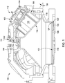
- FIG. 1 depicts a cross-sectional view of a multi-cathode process chamber (process chamber 100) in accordance with some embodiments of the present disclosure.
- the process chamber 100 includes a plurality of cathodes 102 coupled to an upper portion of the process chamber 100, a rotating shield 106 to selectively cover one or more of the plurality of cathodes 102, and a substrate support 110 disposed within the process chamber 100 below the plurality of cathodes 102.
- the substrate support 110 may be a rotating pedestal.
- the substrate support 110 may be vertically movable.
- the plurality of cathodes 102 can be used for sputtering different materials on a substrate 108.
- the substrate 108 is a structure having a semiconductor material used for fabrication of integrated circuits.
- the substrate 108 can represent a semiconductor structure including a wafer.
- the cathodes 102 are exposed through openings or holes 104 of the rotating shield 106, which are disposed over the substrate 108 on the substrate support 110. Materials from the cathodes 102 can be deposited onto the substrate 108 (e.g., materials 103 as shown in Figure 1 ) through the holes 104.
- a power supply 112 may be coupled to each of the plurality of cathodes 102.
- the power supply 112 may include direct current (DC), pulsed DC, or radio frequency (RF) power.
- the rotating shield 106 may expose two or more of the plurality of cathodes 102 and shield remaining cathodes 102 from cross-contamination during sputtering. The cross-contamination results from physical movement or transfer of a deposition material from one of the cathodes 102 to another one of the cathodes 102.
- Each cathode 102 is positioned over a corresponding target 114.
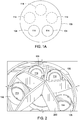
- the rotating shield 106 may have two or more holes 104 to selectively expose corresponding ones or more targets to be co-sputtered (two holes illustratively shown in Figure 1A ). To sputter selected targets, the rotating shield 106 is rotated to expose the selected targets to be sputtered.
- the targets 114 may be formed of any material desired to be sputtered onto the substrate 108.
- a motor 131 is coupled to the rotating shield 106 via a shaft 132 to facilitate the rotation of the rotating shield 106.
- each cathode 102 includes a shroud 126 which is a long tube that does not block a line of sight from the target 114 to a substrate disposed on the substrate support 110.
- Each shroud 126 includes a shroud rotation 128 to provide the cathodes 102 at an angle 130 of about 20 to 90 degrees. Different values of the angle 130 provide different uniformity profiles on a surface of the substrate. The angle 130 is measured between a plane of one of the targets 114 and a plane of the substrate support 110.
- Each shroud is configured to capture a majority of the target flux that is not directed towards and hence likely to land on substrate. As such, the shrouds significantly minimize target cross contamination. Additionally, the shroud material and surface treatment of the shroud may be tailored to specific target materials, thus improving defect performance.
- the substrate 108 Before the substrate 108 moves into or out of the chamber, the substrate 108 can move below a conical shield 118 disposed on a lower portion of the process chamber.
- a telescopic cover ring 120 is disposed on top of the conical shield 118 and surrounds the substrate 108.
- the substrate support 110 moves down, the substrate 108 can be lifted up with a robotic arm before the substrate 108 moves out of the chamber.
- the telescopic cover ring 120 can include a ring portion 122 that curves up and has a predefined thickness to form a dish or bowl in which the substrate can be disposed with the ring portion 122 surrounding and disposed above the substrate 108.
- the telescopic cover ring 120 can also include a predefined gap 124 and a predefined length with respect to the conical shield 118.
- Figure 2 depicts an isometric view of an alternative shield for use in a multi-cathode process chamber, such as the process chamber 100, which can be used in place of the rotating shield 106.
- a process shield (process shield 200) may be used to achieve similar results as the rotating shield 106, described above, but without any rotating parts.
- the process shield 200 extends between adjacent pairs of targets.
- the process shield 200 may comprise several walls disposed between adjacent targets.
- the process shield 200 may be star-shaped, for example, comprising several walls coupled at a centerline and extending radially outward toward the edges of the process cavity to prevent a direct line of site from a given target to any of the other targets.
- the process shield 200 may further include an outer wall (not shown) connecting the walls extending outward from the centerline to surround each target.
- the plurality of targets includes five targets and the process cavity is divided into five equivalent sections by the process shield 200.
- the process shield 200 has a length sufficient to avoid cross talk between targets 114.
- all of the targets 114 may be exposed so that any of the targets 114 may be selected for sputtering.
- the process shield 200 significantly reduces contamination of a non-sputtered target by a sputtered target by an order of magnitude more than without any shield or shrouds.
- the process shield 200 advantageously allows for the flexibility of choosing any one or more of targets to be sputtered without having to move any parts to selectively expose the targets to be sputtered.
- the process shield 200 may optionally have Z-Theta motion, so that sections of the process shield 200 may be positioned at different cathodes 102 during deposition on the substrate and, subsequently, rotated to different cathodes 102 during a paste step.
- the Z-theta motion comprises vertical movement of the process shield 200 followed by rotational movement to selectively expose a given section of the process shield 200, which was originally surrounding one of the targets 114, to a different one of the targets 114.
- the stress associated from deposition of materials from the deposition and paste cathodes at least partially offset each other, advantageously yielding a very low stress film with improved particle performance.
- materials deposited on a given section of the process shield 200 during a first step may exhibit a tensile stress.
- the process shield 200 is rotated so that the given section is disposed around a cathode yielding a material that exhibits a compressive stress.
- the tensile and compressive forces from the two different materials deposited on the given section offset each other.
- flexibility of co-sputtering from any number of cathodes is possible.
- each cathode 102 may alternatively include a shroud 226, which is shorter than the shrouds 126 depicted in the Figure 1 .
- the shrouds 226 may advantageously significantly reduce or eliminate contamination of the top adapter.
- the shrouds 226 may be about 1 inch (about 2.54 cm) long as opposed to the shrouds 126, which may be between about 5 inches (about 12.7 cm) and about 6 inches (about 15.24 cm) long.
- the shrouds 226 may be formed of aluminum or any other metal that has desirable thermal conductivity and surface finish to facilitate adherence of the sputtered material onto the shroud.
- the shrouds 226 may be texturized to improve particle adhesion.
- the shrouds 226 may be bead-blasted or coated with a coating to facilitate adherence of the sputtered material onto the shroud.
- the shrouds 126 of Figure 1 may be similarly texturized.
- the coating may be formed of an aluminum arc spray, a tantalum arc spray, a molybdenum arc spray, or the like.
- the process shield 200 may have any shape that divides each cathode 102 into a separate space without interfering with the deposition of the sputtered material onto the substrate being processed.
- the star shaped process shield 200 has a height less than about 15 inches (about 38.1 cm). The more the height of the process shield 200 exceeds 15 inches (38.1 cm), the more the process shield 200 begins to interfere with the deposition of the sputtered material onto the substrate being processed. If the target diameter is greater than 6 inches (15.24 cm), then the height of the process shield 200 may also be greater than 15 inches (38.1 cm) without adversely affecting the deposition process.
- the height of the process shield 200 is proportional to the diameter of each of the targets. In any case, each target has a diameter at least half of the diameter of the substrate to be processed.
- Figure 3 is a flow chart depicting a method of co-sputtering a plurality of targets.
- a first set of a plurality of targets is exposed through two or more holes of a process shield (e.g., rotating shield 106) while the remaining targets are covered by the shield.
- a process shield e.g., rotating shield 106
- the first set of targets is co-sputtered.
- DC or RF energy may be applied to each of the first set of targets to sputter material from the first set of targets onto the substrate.
- a process gas is supplied into the chamber, a plasma is formed from the process gas using RF energy supplied from each respective cathode, and ions from the plasma are caused to bombard the target to sputter materials from the respective target onto the substrate.
- the shield 106 is rotated to expose a second set of the plurality of targets while covering the remaining targets (i.e., the first set of targets and/or additional ones of the plurality of targets).
- the second set of targets is co-sputtered in a similar manner as the first set of targets, as detailed above. Because each target 114 includes a corresponding shroud 126, the accumulation of target material on a given shroud corresponds to one target. As such, cross-contamination is advantageously avoided. In some embodiments, targets that are not exposed through holes in the shield 106 may be sputtered onto the backside of the shield 106 in a cleaning process so that a cleaner film may be deposited onto the substrate from the cleaned target.
- the plurality of targets are all exposed and one or more of the targets are sputtered, as desired. That is, the method for co-sputtering targets using the process shield 200 is similar to the method 300, except that there is no need to expose a first and second set of targets to co-sputter each set. Instead, because all the targets are exposed in the embodiments in which the process shield 200 is used, a first set of the plurality of targets 114 is co-sputtered and, subsequently, a second set (different than the first set) of the plurality of targets 114 is co-sputtered. Because the process shield 200 is of sufficient height to avoid cross-contamination of the targets, rotation of the shield is not necessary to selectively expose different sets of targets. Thus, throughput is advantageously increased. In some embodiments, the process shield 200 may be coupled to the rotating shield 106 to provide further protection from cross-contamination.
Landscapes
- Chemical & Material Sciences (AREA)
- Engineering & Computer Science (AREA)
- Physics & Mathematics (AREA)
- Plasma & Fusion (AREA)
- Analytical Chemistry (AREA)
- Materials Engineering (AREA)
- Chemical Kinetics & Catalysis (AREA)
- Mechanical Engineering (AREA)
- Metallurgy (AREA)
- Organic Chemistry (AREA)
- Health & Medical Sciences (AREA)
- Toxicology (AREA)
- Epidemiology (AREA)
- Public Health (AREA)
- Physical Vapour Deposition (AREA)
Description
- Embodiments of the present disclosure relate to methods and apparatus for depositing materials on a substrate by physical vapor deposition (PVD).
- Physical vapor deposition (PVD) in semiconductor fabrication is typically performed with a target made of a desired film material. In the case of alloys, the targets are typically composed of the alloy to be sputtered. In the case of new nonvolatile memories, alloys of different compositions are used. As such, the inventors are investigating co-sputtering of multiple targets in a multi-cathode (e.g., multi-target) PVD chamber. However, because of the cross-contamination of the multiple targets, the targets are cleaned periodically to maintain film consistency. For example, one or more of the multiple targets may be covered by shutters during the cleaning process, which may lead to particle generation.
- Therefore, the inventors have provided embodiments of methods and apparatus for improved co-sputtering of multiple target materials in a PVD processing system. Prior art document
WO-A1 -2012/033198 relates to a sputtering apparatus including a plurality of targets, a ground shield, and a shutter mechanism having two rotatable shutters.US-A1-2013/0014700 discloses a multi-target deposition arrangement comprising a rotating target assembly turret and a shield arrangement that includes at least a set of static shields and a set of dynamic shields. The set of static shields is attached to the target assembly turret. The set of dynamic shields is aligned with the set of static shields when a first target is rotated into an operational position for sputtering, wherein the shield arrangement prevents cross contamination to other targets when the sputtering is occurring to the first target.US-B1-6290826 discloses a sputtering apparatus comprising a composite sputtering cathode assembly. The composite sputtering cathode assembly has a plurality of targets and a plurality of shields each disposed between adjacent ones of the targets.US-A1-2014/0034489 discloses a film-forming apparatus including a plurality of target electrodes, and a shutter member rotatably provided between the plurality of target electrodes and the substrate holder and having a plurality of openings and separating walls. - Embodiments of a method and apparatus for co-sputtering multiple target materials are provided herein. In an embodiment of the invention, a process chamber is defined in claim 1.
- In another embodiment of the invention, a physical vapor deposition (PVD) chamber is defined in claim 8.
- In yet another embodiment of the invention, a method of processing a substrate is defined in claim 13.
- Other and further embodiments of the present disclosure are described below.
- Embodiments of the present disclosure, briefly summarized above and discussed in greater detail below, can be understood by reference to the illustrative embodiments of the disclosure depicted in the appended drawings. However, the appended drawings illustrate only typical embodiments of the disclosure and are therefore not to be considered limiting of scope, for the disclosure may admit to other equally effective embodiments.
-
Figure 1 depicts a cross-sectional view of a multi-cathode processing chamber in accordance with some embodiments of the present disclosure. -
Figure 1A depicts a bottom schematic view of a rotating shield in the multi-cathode processing chamber ofFigure 1 . -
Figure 2 depicts an isometric view of a shield for use in a multi-cathode processing chamber in accordance with some embodiments of the present disclosure. -
Figure 3 is a flowchart depicting a method of processing a substrate in accordance with some embodiments of the present disclosure. - To facilitate understanding, identical reference numerals have been used, where possible, to designate identical elements that are common to the figures. The figures are not drawn to scale and may be simplified for clarity. Elements and features of one embodiment may be beneficially incorporated in other embodiments without further recitation.
- Embodiments of methods and apparatus for co-sputtering multiple target materials are provided herein. The disclosed methods and apparatus may advantageously allow co-sputtering of a plurality of targets while substantially minimizing or eliminating cross-contamination between targets.
- In some embodiments, a multi cathode-PVD chamber includes a plurality of cathodes, or targets, (for example, 5 cathodes) attached to a top adapter. Each cathode can have a DC/Pulse DC or RF target and an associated magnetron. Each cathode also has a shroud which is long tube which does not block a line of sight from the target to wafer. A common rotating shield is provided in the center of the chamber that is shared by all the cathodes. Depending on the number of targets that need to be sputtered at the same time, the rotating shield can have one or more holes, such as 1, 2, or 3 holes. The shroud surrounding each target advantageously captures a majority of the target flux that is not directed towards the wafer and hence likely to land on the wafer, thus significantly minimizing target cross-contamination. In some embodiments, the shroud material and surface treatment can be tailored to a specific target material being sputtered, thus improving defect performance.
- In some embodiments, a process shield can be provided to divide the process cavity into a number of sections corresponding to each cathode target. The process shield advantageously similarly limits or eliminates cross-contamination but with no rotating parts. For example, in some embodiments where five cathodes are provided, the process cavity can be divided into 5 equal sections with a process shield that is shaped like a star. The process shield is as long as possible to avoid cross talk. In some embodiments, the process shield can have Z-Theta motion. In such embodiments, the process shield can be positioned at different cathodes during deposition on the wafer. Then during a paste step the process shield can be rotated to a different cathode. The deposited stress from materials from the deposition and paste cathodes can cancel each other or at least reduce stress in the film deposited on the process shield, thus yielding a very low stress film with very good particle performance. When using a process shield as described herein, flexibility of co-sputtering from any number of cathodes is possible.
-
Figure 1 depicts a cross-sectional view of a multi-cathode process chamber (process chamber 100) in accordance with some embodiments of the present disclosure. Theprocess chamber 100 includes a plurality ofcathodes 102 coupled to an upper portion of theprocess chamber 100, arotating shield 106 to selectively cover one or more of the plurality ofcathodes 102, and asubstrate support 110 disposed within theprocess chamber 100 below the plurality ofcathodes 102. In some embodiments, thesubstrate support 110 may be a rotating pedestal. In some embodiments, thesubstrate support 110 may be vertically movable. - The plurality of
cathodes 102 can be used for sputtering different materials on asubstrate 108. In some embodiments, thesubstrate 108 is a structure having a semiconductor material used for fabrication of integrated circuits. For example, thesubstrate 108 can represent a semiconductor structure including a wafer. - The
cathodes 102 are exposed through openings orholes 104 of the rotatingshield 106, which are disposed over thesubstrate 108 on thesubstrate support 110. Materials from thecathodes 102 can be deposited onto the substrate 108 (e.g.,materials 103 as shown inFigure 1 ) through theholes 104. - A
power supply 112 may be coupled to each of the plurality ofcathodes 102. Thepower supply 112 may include direct current (DC), pulsed DC, or radio frequency (RF) power. The rotatingshield 106 may expose two or more of the plurality ofcathodes 102 andshield remaining cathodes 102 from cross-contamination during sputtering. The cross-contamination results from physical movement or transfer of a deposition material from one of thecathodes 102 to another one of thecathodes 102. Eachcathode 102 is positioned over acorresponding target 114. Depending on the number oftargets 114 that need to be sputtered, therotating shield 106 may have two ormore holes 104 to selectively expose corresponding ones or more targets to be co-sputtered (two holes illustratively shown inFigure 1A ). To sputter selected targets, therotating shield 106 is rotated to expose the selected targets to be sputtered. Thetargets 114 may be formed of any material desired to be sputtered onto thesubstrate 108. Amotor 131 is coupled to therotating shield 106 via ashaft 132 to facilitate the rotation of therotating shield 106. - In some embodiments, each
cathode 102 includes ashroud 126 which is a long tube that does not block a line of sight from thetarget 114 to a substrate disposed on thesubstrate support 110. Eachshroud 126 includes ashroud rotation 128 to provide thecathodes 102 at anangle 130 of about 20 to 90 degrees. Different values of theangle 130 provide different uniformity profiles on a surface of the substrate. Theangle 130 is measured between a plane of one of thetargets 114 and a plane of thesubstrate support 110. Each shroud is configured to capture a majority of the target flux that is not directed towards and hence likely to land on substrate. As such, the shrouds significantly minimize target cross contamination. Additionally, the shroud material and surface treatment of the shroud may be tailored to specific target materials, thus improving defect performance. - Before the
substrate 108 moves into or out of the chamber, thesubstrate 108 can move below aconical shield 118 disposed on a lower portion of the process chamber. Atelescopic cover ring 120 is disposed on top of theconical shield 118 and surrounds thesubstrate 108. When thesubstrate support 110 moves down, thesubstrate 108 can be lifted up with a robotic arm before thesubstrate 108 moves out of the chamber. - The
telescopic cover ring 120 can include aring portion 122 that curves up and has a predefined thickness to form a dish or bowl in which the substrate can be disposed with thering portion 122 surrounding and disposed above thesubstrate 108. Thetelescopic cover ring 120 can also include apredefined gap 124 and a predefined length with respect to theconical shield 118. Thus, whenmaterials 103 are deposited on thesubstrate 108, thematerials 103 are prevented or substantially prevented from depositing below thesubstrate support 110 or outside of theconical shield 118. Controlling the deposition ofmaterials 103 as described advantageously prevents or reduces the spread of contaminants to thesubstrate 108 or within the process chamber. -
Figure 2 depicts an isometric view of an alternative shield for use in a multi-cathode process chamber, such as theprocess chamber 100, which can be used in place of therotating shield 106. In some embodiments, a process shield (process shield 200) may be used to achieve similar results as therotating shield 106, described above, but without any rotating parts. In such embodiments, theprocess shield 200 extends between adjacent pairs of targets. In some embodiments, theprocess shield 200 may comprise several walls disposed between adjacent targets. In some embodiments, and as shown inFigure 2 , theprocess shield 200 may be star-shaped, for example, comprising several walls coupled at a centerline and extending radially outward toward the edges of the process cavity to prevent a direct line of site from a given target to any of the other targets. In some embodiments, theprocess shield 200 may further include an outer wall (not shown) connecting the walls extending outward from the centerline to surround each target. In some embodiments, the plurality of targets includes five targets and the process cavity is divided into five equivalent sections by theprocess shield 200. Theprocess shield 200 has a length sufficient to avoid cross talk betweentargets 114. In some embodiments, all of thetargets 114 may be exposed so that any of thetargets 114 may be selected for sputtering. In the embodiment in which all of the targets are exposed, theprocess shield 200 significantly reduces contamination of a non-sputtered target by a sputtered target by an order of magnitude more than without any shield or shrouds. In addition, theprocess shield 200 advantageously allows for the flexibility of choosing any one or more of targets to be sputtered without having to move any parts to selectively expose the targets to be sputtered. - In some embodiments, the
process shield 200 may optionally have Z-Theta motion, so that sections of theprocess shield 200 may be positioned atdifferent cathodes 102 during deposition on the substrate and, subsequently, rotated todifferent cathodes 102 during a paste step. The Z-theta motion comprises vertical movement of theprocess shield 200 followed by rotational movement to selectively expose a given section of theprocess shield 200, which was originally surrounding one of thetargets 114, to a different one of thetargets 114. The stress associated from deposition of materials from the deposition and paste cathodes at least partially offset each other, advantageously yielding a very low stress film with improved particle performance. For example, materials deposited on a given section of theprocess shield 200 during a first step may exhibit a tensile stress. To offset the tensile stress in the material deposited on the given section, theprocess shield 200 is rotated so that the given section is disposed around a cathode yielding a material that exhibits a compressive stress. As a result, the tensile and compressive forces from the two different materials deposited on the given section offset each other. Thus, when using theprocess shield 200, flexibility of co-sputtering from any number of cathodes is possible. - In some embodiments, the
cathodes 102 do not include shrouds since theprocess shield 200 significantly reduces or eliminates cross-contamination oftargets 114 being co-sputtered. In some embodiments, eachcathode 102 may alternatively include a shroud 226, which is shorter than theshrouds 126 depicted in theFigure 1 . The shrouds 226 may advantageously significantly reduce or eliminate contamination of the top adapter. For example, the shrouds 226 may be about 1 inch (about 2.54 cm) long as opposed to theshrouds 126, which may be between about 5 inches (about 12.7 cm) and about 6 inches (about 15.24 cm) long. In some embodiments, the shrouds 226 may be formed of aluminum or any other metal that has desirable thermal conductivity and surface finish to facilitate adherence of the sputtered material onto the shroud. In some embodiments, the shrouds 226 may be texturized to improve particle adhesion. For example, the shrouds 226 may be bead-blasted or coated with a coating to facilitate adherence of the sputtered material onto the shroud. In some embodiments, theshrouds 126 ofFigure 1 may be similarly texturized. In some embodiments, for example, the coating may be formed of an aluminum arc spray, a tantalum arc spray, a molybdenum arc spray, or the like. - Although depicted as star-shaped, the
process shield 200 may have any shape that divides eachcathode 102 into a separate space without interfering with the deposition of the sputtered material onto the substrate being processed. For example, assuming eachtarget 114 has a diameter of about 6 inches (about 15.24 cm), the star shapedprocess shield 200 has a height less than about 15 inches (about 38.1 cm). The more the height of theprocess shield 200 exceeds 15 inches (38.1 cm), the more theprocess shield 200 begins to interfere with the deposition of the sputtered material onto the substrate being processed. If the target diameter is greater than 6 inches (15.24 cm), then the height of theprocess shield 200 may also be greater than 15 inches (38.1 cm) without adversely affecting the deposition process. In other words, the height of theprocess shield 200 is proportional to the diameter of each of the targets. In any case, each target has a diameter at least half of the diameter of the substrate to be processed. -
Figure 3 is a flow chart depicting a method of co-sputtering a plurality of targets. At 302, a first set of a plurality of targets is exposed through two or more holes of a process shield (e.g., rotating shield 106) while the remaining targets are covered by the shield. - At 304, the first set of targets is co-sputtered. For example, DC or RF energy may be applied to each of the first set of targets to sputter material from the first set of targets onto the substrate. In some embodiments, a process gas is supplied into the chamber, a plasma is formed from the process gas using RF energy supplied from each respective cathode, and ions from the plasma are caused to bombard the target to sputter materials from the respective target onto the substrate.
- Optionally at 304, if another set of targets, different than the first set, is to be sputtered, the
shield 106 is rotated to expose a second set of the plurality of targets while covering the remaining targets (i.e., the first set of targets and/or additional ones of the plurality of targets). - At 306, the second set of targets is co-sputtered in a similar manner as the first set of targets, as detailed above. Because each
target 114 includes acorresponding shroud 126, the accumulation of target material on a given shroud corresponds to one target. As such, cross-contamination is advantageously avoided. In some embodiments, targets that are not exposed through holes in theshield 106 may be sputtered onto the backside of theshield 106 in a cleaning process so that a cleaner film may be deposited onto the substrate from the cleaned target. - In embodiments in which the
process shield 200 is utilized, the plurality of targets are all exposed and one or more of the targets are sputtered, as desired. That is, the method for co-sputtering targets using theprocess shield 200 is similar to themethod 300, except that there is no need to expose a first and second set of targets to co-sputter each set. Instead, because all the targets are exposed in the embodiments in which theprocess shield 200 is used, a first set of the plurality oftargets 114 is co-sputtered and, subsequently, a second set (different than the first set) of the plurality oftargets 114 is co-sputtered. Because theprocess shield 200 is of sufficient height to avoid cross-contamination of the targets, rotation of the shield is not necessary to selectively expose different sets of targets. Thus, throughput is advantageously increased. In some embodiments, theprocess shield 200 may be coupled to therotating shield 106 to provide further protection from cross-contamination. - While the foregoing is directed to embodiments of the present disclosure, other and further embodiments of the disclosure may be devised without departing from the basic scope thereof. The invention is defined by the claims.
Claims (14)
- A process chamber (100), comprising:a substrate support (110) arranged to support a substrate (108);a plurality of cathodes (102) coupled to a carrier and having a corresponding plurality of targets (114) to be sputtered onto the substrate (108); anda process shield (200) coupled to the carrier and extending between adjacent pairs of the plurality of targets (114), wherein the process shield (200) is configured to move vertically and rotate with respect to the plurality of cathodes (102).
- The process chamber of claim 1, wherein the process shield (200) is star-shaped.
- The process chamber of claim 1, wherein the process shield is arranged such that all of the plurality of targets (114) are exposed.
- The process chamber of any of claims 1 to 3, wherein a height of the process shield (200) is proportional to a diameter of each of the plurality of targets (114).
- The process chamber of any of claims 1 to 3, further comprising:
a plurality of shrouds (126) each surrounding a corresponding one of the plurality of targets (114). - The process chamber of claim 5, wherein each of the plurality of shrouds (126) has a height of about 1 inch (about 2.54 cm).
- The process chamber of claim 5, wherein the plurality of shrouds (126) are formed of aluminum.
- A physical vapor deposition (PVD) chamber, comprising:a substrate support (110) arranged to support a substrate (108);a plurality of targets (114) disposed opposite the substrate support (110), each target comprising a material to be sputtered onto the substrate (108);a shield (106) rotatably disposed between the substrate support (110) and the plurality of targets (114), wherein the shield includes two or more holes (104) sized and positioned to simultaneously expose a set of two or more of the plurality of targets (114) while covering the remainder of the plurality of targets (114), wherein the shield (106) is configured such that different sets of two or more of the plurality of targets (114) can be exposed while covering the remainder of the plurality of targets (114) by selection of the rotational position of the shield (106); anda process shield (200) coupled to the shield (106) and extending between adjacent pairs of the plurality of targets (114).
- The PVD chamber of claim 8, further comprising:
a plurality of shrouds (126) disposed between the shield (106) and the plurality of targets (114), wherein each of the plurality of shrouds surrounds a corresponding one of the plurality of targets. - The PVD chamber of claim 9, wherein the plurality of shrouds (126) are formed of aluminum.
- The PVD chamber of claim 10, wherein the plurality of shrouds (126) are texturized to improve particle adhesion of the plurality of shrouds.
- The PVD chamber of any of claims 9 to 11, wherein each of the plurality of shrouds (126) has a height of about 5 inches (about 12.7 cm) to about 6 inches (about 15.24 cm).
- A method for processing a substrate, comprising:exposing (302) a first set of a plurality of targets (114) through two or more holes (104) of a shield (106), wherein the shield is rotatably coupled to a carrier disposed above a substrate support (110) supporting a substrate (108), and wherein a process shield (200) is coupled to the shield (106) and extends between adjacent pairs of the plurality of targets (114); andco-sputtering (304) the first set of the plurality of targets (114).
- The method of claim 13, further comprising:rotating the shield (106) to expose a second set of the plurality of targets (114) different than the first set; andco-sputtering (306) the second set of the plurality of targets (114).
Applications Claiming Priority (3)
| Application Number | Priority Date | Filing Date | Title |
|---|---|---|---|
| IN2595DE2015 | 2015-08-21 | ||
| US15/240,927 US10468238B2 (en) | 2015-08-21 | 2016-08-18 | Methods and apparatus for co-sputtering multiple targets |
| PCT/US2016/047849 WO2017035008A1 (en) | 2015-08-21 | 2016-08-19 | Method and apparatus for co-sputtering multiple targets |
Publications (3)
| Publication Number | Publication Date |
|---|---|
| EP3337914A1 EP3337914A1 (en) | 2018-06-27 |
| EP3337914A4 EP3337914A4 (en) | 2019-04-17 |
| EP3337914B1 true EP3337914B1 (en) | 2021-03-03 |
Family
ID=58157818
Family Applications (1)
| Application Number | Title | Priority Date | Filing Date |
|---|---|---|---|
| EP16839899.8A Active EP3337914B1 (en) | 2015-08-21 | 2016-08-19 | Method and apparatus for co-sputtering multiple targets |
Country Status (6)
| Country | Link |
|---|---|
| US (2) | US10468238B2 (en) |
| EP (1) | EP3337914B1 (en) |
| JP (1) | JP6916789B2 (en) |
| KR (1) | KR102667749B1 (en) |
| CN (1) | CN107923033B (en) |
| TW (1) | TWI703236B (en) |
Families Citing this family (30)
| Publication number | Priority date | Publication date | Assignee | Title |
|---|---|---|---|---|
| US10224224B2 (en) | 2017-03-10 | 2019-03-05 | Micromaterials, LLC | High pressure wafer processing systems and related methods |
| US10622214B2 (en) | 2017-05-25 | 2020-04-14 | Applied Materials, Inc. | Tungsten defluorination by high pressure treatment |
| US10388533B2 (en) | 2017-06-16 | 2019-08-20 | Applied Materials, Inc. | Process integration method to tune resistivity of nickel silicide |
| US10276411B2 (en) | 2017-08-18 | 2019-04-30 | Applied Materials, Inc. | High pressure and high temperature anneal chamber |
| KR102405723B1 (en) | 2017-08-18 | 2022-06-07 | 어플라이드 머티어리얼스, 인코포레이티드 | High pressure and high temperature annealing chamber |
| EP3707746B1 (en) | 2017-11-11 | 2023-12-27 | Micromaterials LLC | Gas delivery system for high pressure processing chamber |
| JP2021503714A (en) | 2017-11-17 | 2021-02-12 | アプライド マテリアルズ インコーポレイテッドApplied Materials,Incorporated | Capacitor system for high pressure processing system |
| JP7001448B2 (en) * | 2017-12-05 | 2022-01-19 | 東京エレクトロン株式会社 | PVD processing method and PVD processing equipment |
| KR102702244B1 (en) | 2018-03-09 | 2024-09-03 | 어플라이드 머티어리얼스, 인코포레이티드 | High pressure annealing process for metal containing materials |
| US10916433B2 (en) | 2018-04-06 | 2021-02-09 | Applied Materials, Inc. | Methods of forming metal silicide layers and metal silicide layers formed therefrom |
| US10950429B2 (en) | 2018-05-08 | 2021-03-16 | Applied Materials, Inc. | Methods of forming amorphous carbon hard mask layers and hard mask layers formed therefrom |
| KR102180440B1 (en) | 2018-05-18 | 2020-11-18 | (주)이노시아 | Sputtering apparatus and sputtering method |
| US11275300B2 (en) | 2018-07-06 | 2022-03-15 | Applied Materials Inc. | Extreme ultraviolet mask blank defect reduction |
| US10748783B2 (en) | 2018-07-25 | 2020-08-18 | Applied Materials, Inc. | Gas delivery module |
| CN110819964A (en) * | 2018-08-13 | 2020-02-21 | 中兴通讯股份有限公司 | Vacuum coating equipment, method and preparation method of filter cavity film layer |
| WO2020117462A1 (en) | 2018-12-07 | 2020-06-11 | Applied Materials, Inc. | Semiconductor processing system |
| TWI845579B (en) | 2018-12-21 | 2024-06-21 | 美商應用材料股份有限公司 | Extreme ultraviolet mask absorber and processes for manufacture |
| TWI842830B (en) * | 2019-03-01 | 2024-05-21 | 美商應用材料股份有限公司 | Physical vapor deposition chamber and method of depositing alternating material layers |
| TWI870386B (en) | 2019-03-01 | 2025-01-21 | 美商應用材料股份有限公司 | Euv mask blank and the method making the same |
| TWI818151B (en) * | 2019-03-01 | 2023-10-11 | 美商應用材料股份有限公司 | Physical vapor deposition chamber and method of operation thereof |
| TWI845648B (en) | 2019-04-19 | 2024-06-21 | 美商應用材料股份有限公司 | Bragg reflector, extreme ultraviolet (euv) mask blank comprising the same, and method of manufacturing the same |
| KR20220038113A (en) * | 2019-07-25 | 2022-03-25 | 어드밴스드 에너지 인더스트리즈 인코포레이티드 | Pulsed DC sputtering systems and methods |
| US11901222B2 (en) | 2020-02-17 | 2024-02-13 | Applied Materials, Inc. | Multi-step process for flowable gap-fill film |
| US11479847B2 (en) * | 2020-10-14 | 2022-10-25 | Alluxa, Inc. | Sputtering system with a plurality of cathode assemblies |
| US11545347B2 (en) * | 2020-11-05 | 2023-01-03 | Applied Materials, Inc. | Internally divisible process chamber using a shutter disk assembly |
| CN112553587A (en) * | 2020-12-23 | 2021-03-26 | 长沙元戎科技有限责任公司 | Rotary multi-target magnetron sputtering cathode |
| US11815803B2 (en) | 2021-08-30 | 2023-11-14 | Applied Materials, Inc. | Multilayer extreme ultraviolet reflector materials |
| US11782337B2 (en) | 2021-09-09 | 2023-10-10 | Applied Materials, Inc. | Multilayer extreme ultraviolet reflectors |
| JP2023084589A (en) * | 2021-12-07 | 2023-06-19 | 東京エレクトロン株式会社 | Sputtering device and control method |
| JP2025508711A (en) * | 2022-02-14 | 2025-04-10 | アプライド マテリアルズ インコーポレイテッド | Apparatus and method for producing PVD perovskite films |
Family Cites Families (16)
| Publication number | Priority date | Publication date | Assignee | Title |
|---|---|---|---|---|
| DE3821207A1 (en) * | 1988-06-23 | 1989-12-28 | Leybold Ag | ARRANGEMENT FOR COATING A SUBSTRATE WITH DIELECTRICS |
| EP0837491A3 (en) * | 1996-10-21 | 2000-11-15 | Nihon Shinku Gijutsu Kabushiki Kaisha | Composite sputtering cathode assembly and sputtering apparatus with such composite sputtering cathode assembly |
| JP3808148B2 (en) * | 1996-10-21 | 2006-08-09 | 株式会社アルバック | Composite sputtering cathode and sputtering apparatus using the cathode |
| WO1998031845A1 (en) | 1997-01-16 | 1998-07-23 | Bottomfield, Layne, F. | Vapor deposition components and corresponding methods |
| JP4137277B2 (en) | 1999-04-15 | 2008-08-20 | 株式会社アルバック | Sputtering equipment |
| US20020144903A1 (en) * | 2001-02-09 | 2002-10-10 | Plasmion Corporation | Focused magnetron sputtering system |
| JP4437290B2 (en) * | 2003-05-14 | 2010-03-24 | シーワイジー技術研究所株式会社 | Sputtering equipment |
| JP4494047B2 (en) * | 2004-03-12 | 2010-06-30 | キヤノンアネルバ株式会社 | Double shutter control method for multi-source sputtering deposition system |
| US7785455B2 (en) * | 2005-04-14 | 2010-08-31 | Tango Systems, Inc. | Cross-contaminant shield in sputtering system |
| US8771483B2 (en) | 2007-09-05 | 2014-07-08 | Intermolecular, Inc. | Combinatorial process system |
| JP5584409B2 (en) * | 2008-02-21 | 2014-09-03 | キヤノンアネルバ株式会社 | Sputtering apparatus and control method thereof |
| WO2012033198A1 (en) | 2010-09-10 | 2012-03-15 | 株式会社 アルバック | Sputtering apparatus |
| KR101583122B1 (en) * | 2011-04-28 | 2016-01-07 | 캐논 아네르바 가부시키가이샤 | Film-forming apparatus |
| US20130014700A1 (en) | 2011-07-11 | 2013-01-17 | Hariharakeshava Sarpangala Hegde | Target shield designs in multi-target deposition system. |
| JP5865483B2 (en) * | 2012-03-14 | 2016-02-17 | キヤノンアネルバ株式会社 | Fastening member and vacuum device |
| US20140272684A1 (en) | 2013-03-12 | 2014-09-18 | Applied Materials, Inc. | Extreme ultraviolet lithography mask blank manufacturing system and method of operation therefor |
-
2016
- 2016-08-18 US US15/240,927 patent/US10468238B2/en active Active
- 2016-08-19 KR KR1020187007936A patent/KR102667749B1/en active Active
- 2016-08-19 TW TW105126614A patent/TWI703236B/en active
- 2016-08-19 CN CN201680048305.7A patent/CN107923033B/en active Active
- 2016-08-19 JP JP2018528214A patent/JP6916789B2/en active Active
- 2016-08-19 EP EP16839899.8A patent/EP3337914B1/en active Active
-
2019
- 2019-09-17 US US16/573,265 patent/US11101117B2/en active Active
Non-Patent Citations (1)
| Title |
|---|
| None * |
Also Published As
| Publication number | Publication date |
|---|---|
| EP3337914A4 (en) | 2019-04-17 |
| TWI703236B (en) | 2020-09-01 |
| US11101117B2 (en) | 2021-08-24 |
| JP6916789B2 (en) | 2021-08-11 |
| US20200013597A1 (en) | 2020-01-09 |
| KR102667749B1 (en) | 2024-05-20 |
| US20170053784A1 (en) | 2017-02-23 |
| CN107923033B (en) | 2020-11-27 |
| KR20180034679A (en) | 2018-04-04 |
| JP2018528330A (en) | 2018-09-27 |
| US10468238B2 (en) | 2019-11-05 |
| EP3337914A1 (en) | 2018-06-27 |
| TW201713796A (en) | 2017-04-16 |
| CN107923033A (en) | 2018-04-17 |
Similar Documents
| Publication | Publication Date | Title |
|---|---|---|
| US11101117B2 (en) | Methods and apparatus for co-sputtering multiple targets | |
| US10431440B2 (en) | Methods and apparatus for processing a substrate | |
| TWI756401B (en) | Plasma chamber target for reducing defects in workpiece during dielectric sputtering | |
| US11043364B2 (en) | Process kit for multi-cathode processing chamber | |
| WO2017035008A1 (en) | Method and apparatus for co-sputtering multiple targets | |
| KR102284028B1 (en) | Single Oxide Metal Deposition Chamber | |
| US11361950B2 (en) | Multi-cathode processing chamber with dual rotatable shields | |
| CN115244210B (en) | Plasma chamber targets for reducing defects in workpieces during dielectric sputtering | |
| WO2022098445A1 (en) | Internally divisible process chamber using a shutter disk assembly |
Legal Events
| Date | Code | Title | Description |
|---|---|---|---|
| STAA | Information on the status of an ep patent application or granted ep patent |
Free format text: STATUS: THE INTERNATIONAL PUBLICATION HAS BEEN MADE |
|
| PUAI | Public reference made under article 153(3) epc to a published international application that has entered the european phase |
Free format text: ORIGINAL CODE: 0009012 |
|
| STAA | Information on the status of an ep patent application or granted ep patent |
Free format text: STATUS: REQUEST FOR EXAMINATION WAS MADE |
|
| 17P | Request for examination filed |
Effective date: 20180302 |
|
| AK | Designated contracting states |
Kind code of ref document: A1 Designated state(s): AL AT BE BG CH CY CZ DE DK EE ES FI FR GB GR HR HU IE IS IT LI LT LU LV MC MK MT NL NO PL PT RO RS SE SI SK SM TR |
|
| AX | Request for extension of the european patent |
Extension state: BA ME |
|
| DAV | Request for validation of the european patent (deleted) | ||
| DAX | Request for extension of the european patent (deleted) | ||
| A4 | Supplementary search report drawn up and despatched |
Effective date: 20190319 |
|
| RIC1 | Information provided on ipc code assigned before grant |
Ipc: H01J 37/32 20060101ALI20190313BHEP Ipc: C23C 14/50 20060101ALI20190313BHEP Ipc: C23C 14/34 20060101AFI20190313BHEP Ipc: H01J 37/34 20060101ALI20190313BHEP Ipc: C23C 14/56 20060101ALI20190313BHEP |
|
| GRAP | Despatch of communication of intention to grant a patent |
Free format text: ORIGINAL CODE: EPIDOSNIGR1 |
|
| STAA | Information on the status of an ep patent application or granted ep patent |
Free format text: STATUS: GRANT OF PATENT IS INTENDED |
|
| INTG | Intention to grant announced |
Effective date: 20200914 |
|
| GRAS | Grant fee paid |
Free format text: ORIGINAL CODE: EPIDOSNIGR3 |
|
| GRAA | (expected) grant |
Free format text: ORIGINAL CODE: 0009210 |
|
| STAA | Information on the status of an ep patent application or granted ep patent |
Free format text: STATUS: THE PATENT HAS BEEN GRANTED |
|
| AK | Designated contracting states |
Kind code of ref document: B1 Designated state(s): AL AT BE BG CH CY CZ DE DK EE ES FI FR GB GR HR HU IE IS IT LI LT LU LV MC MK MT NL NO PL PT RO RS SE SI SK SM TR |
|
| REG | Reference to a national code |
Ref country code: GB Ref legal event code: FG4D |
|
| REG | Reference to a national code |
Ref country code: AT Ref legal event code: REF Ref document number: 1367280 Country of ref document: AT Kind code of ref document: T Effective date: 20210315 Ref country code: CH Ref legal event code: EP |
|
| REG | Reference to a national code |
Ref country code: DE Ref legal event code: R096 Ref document number: 602016053748 Country of ref document: DE |
|
| REG | Reference to a national code |
Ref country code: IE Ref legal event code: FG4D |
|
| REG | Reference to a national code |
Ref country code: LT Ref legal event code: MG9D |
|
| PG25 | Lapsed in a contracting state [announced via postgrant information from national office to epo] |
Ref country code: LT Free format text: LAPSE BECAUSE OF FAILURE TO SUBMIT A TRANSLATION OF THE DESCRIPTION OR TO PAY THE FEE WITHIN THE PRESCRIBED TIME-LIMIT Effective date: 20210303 Ref country code: BG Free format text: LAPSE BECAUSE OF FAILURE TO SUBMIT A TRANSLATION OF THE DESCRIPTION OR TO PAY THE FEE WITHIN THE PRESCRIBED TIME-LIMIT Effective date: 20210603 Ref country code: GR Free format text: LAPSE BECAUSE OF FAILURE TO SUBMIT A TRANSLATION OF THE DESCRIPTION OR TO PAY THE FEE WITHIN THE PRESCRIBED TIME-LIMIT Effective date: 20210604 Ref country code: HR Free format text: LAPSE BECAUSE OF FAILURE TO SUBMIT A TRANSLATION OF THE DESCRIPTION OR TO PAY THE FEE WITHIN THE PRESCRIBED TIME-LIMIT Effective date: 20210303 Ref country code: FI Free format text: LAPSE BECAUSE OF FAILURE TO SUBMIT A TRANSLATION OF THE DESCRIPTION OR TO PAY THE FEE WITHIN THE PRESCRIBED TIME-LIMIT Effective date: 20210303 Ref country code: NO Free format text: LAPSE BECAUSE OF FAILURE TO SUBMIT A TRANSLATION OF THE DESCRIPTION OR TO PAY THE FEE WITHIN THE PRESCRIBED TIME-LIMIT Effective date: 20210603 |
|
| REG | Reference to a national code |
Ref country code: NL Ref legal event code: MP Effective date: 20210303 |
|
| REG | Reference to a national code |
Ref country code: AT Ref legal event code: MK05 Ref document number: 1367280 Country of ref document: AT Kind code of ref document: T Effective date: 20210303 |
|
| PG25 | Lapsed in a contracting state [announced via postgrant information from national office to epo] |
Ref country code: SE Free format text: LAPSE BECAUSE OF FAILURE TO SUBMIT A TRANSLATION OF THE DESCRIPTION OR TO PAY THE FEE WITHIN THE PRESCRIBED TIME-LIMIT Effective date: 20210303 Ref country code: RS Free format text: LAPSE BECAUSE OF FAILURE TO SUBMIT A TRANSLATION OF THE DESCRIPTION OR TO PAY THE FEE WITHIN THE PRESCRIBED TIME-LIMIT Effective date: 20210303 Ref country code: LV Free format text: LAPSE BECAUSE OF FAILURE TO SUBMIT A TRANSLATION OF THE DESCRIPTION OR TO PAY THE FEE WITHIN THE PRESCRIBED TIME-LIMIT Effective date: 20210303 Ref country code: PL Free format text: LAPSE BECAUSE OF FAILURE TO SUBMIT A TRANSLATION OF THE DESCRIPTION OR TO PAY THE FEE WITHIN THE PRESCRIBED TIME-LIMIT Effective date: 20210303 |
|
| PG25 | Lapsed in a contracting state [announced via postgrant information from national office to epo] |
Ref country code: NL Free format text: LAPSE BECAUSE OF FAILURE TO SUBMIT A TRANSLATION OF THE DESCRIPTION OR TO PAY THE FEE WITHIN THE PRESCRIBED TIME-LIMIT Effective date: 20210303 |
|
| PG25 | Lapsed in a contracting state [announced via postgrant information from national office to epo] |
Ref country code: AT Free format text: LAPSE BECAUSE OF FAILURE TO SUBMIT A TRANSLATION OF THE DESCRIPTION OR TO PAY THE FEE WITHIN THE PRESCRIBED TIME-LIMIT Effective date: 20210303 Ref country code: SM Free format text: LAPSE BECAUSE OF FAILURE TO SUBMIT A TRANSLATION OF THE DESCRIPTION OR TO PAY THE FEE WITHIN THE PRESCRIBED TIME-LIMIT Effective date: 20210303 Ref country code: EE Free format text: LAPSE BECAUSE OF FAILURE TO SUBMIT A TRANSLATION OF THE DESCRIPTION OR TO PAY THE FEE WITHIN THE PRESCRIBED TIME-LIMIT Effective date: 20210303 Ref country code: CZ Free format text: LAPSE BECAUSE OF FAILURE TO SUBMIT A TRANSLATION OF THE DESCRIPTION OR TO PAY THE FEE WITHIN THE PRESCRIBED TIME-LIMIT Effective date: 20210303 |
|
| PG25 | Lapsed in a contracting state [announced via postgrant information from national office to epo] |
Ref country code: PT Free format text: LAPSE BECAUSE OF FAILURE TO SUBMIT A TRANSLATION OF THE DESCRIPTION OR TO PAY THE FEE WITHIN THE PRESCRIBED TIME-LIMIT Effective date: 20210705 Ref country code: RO Free format text: LAPSE BECAUSE OF FAILURE TO SUBMIT A TRANSLATION OF THE DESCRIPTION OR TO PAY THE FEE WITHIN THE PRESCRIBED TIME-LIMIT Effective date: 20210303 Ref country code: SK Free format text: LAPSE BECAUSE OF FAILURE TO SUBMIT A TRANSLATION OF THE DESCRIPTION OR TO PAY THE FEE WITHIN THE PRESCRIBED TIME-LIMIT Effective date: 20210303 Ref country code: IS Free format text: LAPSE BECAUSE OF FAILURE TO SUBMIT A TRANSLATION OF THE DESCRIPTION OR TO PAY THE FEE WITHIN THE PRESCRIBED TIME-LIMIT Effective date: 20210703 |
|
| REG | Reference to a national code |
Ref country code: DE Ref legal event code: R097 Ref document number: 602016053748 Country of ref document: DE |
|
| PLBE | No opposition filed within time limit |
Free format text: ORIGINAL CODE: 0009261 |
|
| STAA | Information on the status of an ep patent application or granted ep patent |
Free format text: STATUS: NO OPPOSITION FILED WITHIN TIME LIMIT |
|
| PG25 | Lapsed in a contracting state [announced via postgrant information from national office to epo] |
Ref country code: DK Free format text: LAPSE BECAUSE OF FAILURE TO SUBMIT A TRANSLATION OF THE DESCRIPTION OR TO PAY THE FEE WITHIN THE PRESCRIBED TIME-LIMIT Effective date: 20210303 Ref country code: AL Free format text: LAPSE BECAUSE OF FAILURE TO SUBMIT A TRANSLATION OF THE DESCRIPTION OR TO PAY THE FEE WITHIN THE PRESCRIBED TIME-LIMIT Effective date: 20210303 Ref country code: ES Free format text: LAPSE BECAUSE OF FAILURE TO SUBMIT A TRANSLATION OF THE DESCRIPTION OR TO PAY THE FEE WITHIN THE PRESCRIBED TIME-LIMIT Effective date: 20210303 |
|
| 26N | No opposition filed |
Effective date: 20211206 |
|
| PG25 | Lapsed in a contracting state [announced via postgrant information from national office to epo] |
Ref country code: SI Free format text: LAPSE BECAUSE OF FAILURE TO SUBMIT A TRANSLATION OF THE DESCRIPTION OR TO PAY THE FEE WITHIN THE PRESCRIBED TIME-LIMIT Effective date: 20210303 |
|
| REG | Reference to a national code |
Ref country code: CH Ref legal event code: PL |
|
| PG25 | Lapsed in a contracting state [announced via postgrant information from national office to epo] |
Ref country code: MC Free format text: LAPSE BECAUSE OF FAILURE TO SUBMIT A TRANSLATION OF THE DESCRIPTION OR TO PAY THE FEE WITHIN THE PRESCRIBED TIME-LIMIT Effective date: 20210303 |
|
| GBPC | Gb: european patent ceased through non-payment of renewal fee |
Effective date: 20210819 |
|
| PG25 | Lapsed in a contracting state [announced via postgrant information from national office to epo] |
Ref country code: LI Free format text: LAPSE BECAUSE OF NON-PAYMENT OF DUE FEES Effective date: 20210831 Ref country code: IT Free format text: LAPSE BECAUSE OF FAILURE TO SUBMIT A TRANSLATION OF THE DESCRIPTION OR TO PAY THE FEE WITHIN THE PRESCRIBED TIME-LIMIT Effective date: 20210303 Ref country code: CH Free format text: LAPSE BECAUSE OF NON-PAYMENT OF DUE FEES Effective date: 20210831 |
|
| PG25 | Lapsed in a contracting state [announced via postgrant information from national office to epo] |
Ref country code: IS Free format text: LAPSE BECAUSE OF FAILURE TO SUBMIT A TRANSLATION OF THE DESCRIPTION OR TO PAY THE FEE WITHIN THE PRESCRIBED TIME-LIMIT Effective date: 20210703 Ref country code: LU Free format text: LAPSE BECAUSE OF NON-PAYMENT OF DUE FEES Effective date: 20210819 |
|
| PG25 | Lapsed in a contracting state [announced via postgrant information from national office to epo] |
Ref country code: IE Free format text: LAPSE BECAUSE OF NON-PAYMENT OF DUE FEES Effective date: 20210819 Ref country code: GB Free format text: LAPSE BECAUSE OF NON-PAYMENT OF DUE FEES Effective date: 20210819 |
|
| PG25 | Lapsed in a contracting state [announced via postgrant information from national office to epo] |
Ref country code: HU Free format text: LAPSE BECAUSE OF FAILURE TO SUBMIT A TRANSLATION OF THE DESCRIPTION OR TO PAY THE FEE WITHIN THE PRESCRIBED TIME-LIMIT; INVALID AB INITIO Effective date: 20160819 |
|
| PG25 | Lapsed in a contracting state [announced via postgrant information from national office to epo] |
Ref country code: CY Free format text: LAPSE BECAUSE OF FAILURE TO SUBMIT A TRANSLATION OF THE DESCRIPTION OR TO PAY THE FEE WITHIN THE PRESCRIBED TIME-LIMIT Effective date: 20210303 |
|
| PG25 | Lapsed in a contracting state [announced via postgrant information from national office to epo] |
Ref country code: MK Free format text: LAPSE BECAUSE OF FAILURE TO SUBMIT A TRANSLATION OF THE DESCRIPTION OR TO PAY THE FEE WITHIN THE PRESCRIBED TIME-LIMIT Effective date: 20210303 |
|
| PG25 | Lapsed in a contracting state [announced via postgrant information from national office to epo] |
Ref country code: MT Free format text: LAPSE BECAUSE OF FAILURE TO SUBMIT A TRANSLATION OF THE DESCRIPTION OR TO PAY THE FEE WITHIN THE PRESCRIBED TIME-LIMIT Effective date: 20210303 |
|
| PGFP | Annual fee paid to national office [announced via postgrant information from national office to epo] |
Ref country code: DE Payment date: 20250724 Year of fee payment: 10 |
|
| PGFP | Annual fee paid to national office [announced via postgrant information from national office to epo] |
Ref country code: BE Payment date: 20250723 Year of fee payment: 10 |
|
| PGFP | Annual fee paid to national office [announced via postgrant information from national office to epo] |
Ref country code: FR Payment date: 20250725 Year of fee payment: 10 |
|
| PG25 | Lapsed in a contracting state [announced via postgrant information from national office to epo] |
Ref country code: TR Free format text: LAPSE BECAUSE OF FAILURE TO SUBMIT A TRANSLATION OF THE DESCRIPTION OR TO PAY THE FEE WITHIN THE PRESCRIBED TIME-LIMIT Effective date: 20210303 |