EP3334263B1 - Leiterplatte, entsprechendes beleuchtungsmodul, beleuchtungssystem und verfahren zur implementierung von beleuchtungsmodulen - Google Patents
Leiterplatte, entsprechendes beleuchtungsmodul, beleuchtungssystem und verfahren zur implementierung von beleuchtungsmodulen Download PDFInfo
- Publication number
- EP3334263B1 EP3334263B1 EP17205871.1A EP17205871A EP3334263B1 EP 3334263 B1 EP3334263 B1 EP 3334263B1 EP 17205871 A EP17205871 A EP 17205871A EP 3334263 B1 EP3334263 B1 EP 3334263B1
- Authority
- EP
- European Patent Office
- Prior art keywords
- contacts
- lighting
- positive terminal
- module
- terminal
- Prior art date
- Legal status (The legal status is an assumption and is not a legal conclusion. Google has not performed a legal analysis and makes no representation as to the accuracy of the status listed.)
- Active
Links
Images







Classifications
-
- H—ELECTRICITY
- H05—ELECTRIC TECHNIQUES NOT OTHERWISE PROVIDED FOR
- H05K—PRINTED CIRCUITS; CASINGS OR CONSTRUCTIONAL DETAILS OF ELECTRIC APPARATUS; MANUFACTURE OF ASSEMBLAGES OF ELECTRICAL COMPONENTS
- H05K1/00—Printed circuits
- H05K1/02—Details
- H05K1/0286—Programmable, customizable or modifiable circuits
- H05K1/029—Programmable, customizable or modifiable circuits having a programmable lay-out, i.e. adapted for choosing between a few possibilities
-
- H—ELECTRICITY
- H05—ELECTRIC TECHNIQUES NOT OTHERWISE PROVIDED FOR
- H05B—ELECTRIC HEATING; ELECTRIC LIGHT SOURCES NOT OTHERWISE PROVIDED FOR; CIRCUIT ARRANGEMENTS FOR ELECTRIC LIGHT SOURCES, IN GENERAL
- H05B45/00—Circuit arrangements for operating light-emitting diodes [LED]
- H05B45/40—Details of LED load circuits
- H05B45/44—Details of LED load circuits with an active control inside an LED matrix
- H05B45/48—Details of LED load circuits with an active control inside an LED matrix having LEDs organised in strings and incorporating parallel shunting devices
-
- H—ELECTRICITY
- H05—ELECTRIC TECHNIQUES NOT OTHERWISE PROVIDED FOR
- H05K—PRINTED CIRCUITS; CASINGS OR CONSTRUCTIONAL DETAILS OF ELECTRIC APPARATUS; MANUFACTURE OF ASSEMBLAGES OF ELECTRICAL COMPONENTS
- H05K1/00—Printed circuits
- H05K1/02—Details
- H05K1/11—Printed elements for providing electric connections to or between printed circuits
-
- H—ELECTRICITY
- H05—ELECTRIC TECHNIQUES NOT OTHERWISE PROVIDED FOR
- H05K—PRINTED CIRCUITS; CASINGS OR CONSTRUCTIONAL DETAILS OF ELECTRIC APPARATUS; MANUFACTURE OF ASSEMBLAGES OF ELECTRICAL COMPONENTS
- H05K1/00—Printed circuits
- H05K1/18—Printed circuits structurally associated with non-printed electric components
- H05K1/181—Printed circuits structurally associated with non-printed electric components associated with surface mounted components
-
- H—ELECTRICITY
- H05—ELECTRIC TECHNIQUES NOT OTHERWISE PROVIDED FOR
- H05K—PRINTED CIRCUITS; CASINGS OR CONSTRUCTIONAL DETAILS OF ELECTRIC APPARATUS; MANUFACTURE OF ASSEMBLAGES OF ELECTRICAL COMPONENTS
- H05K13/00—Apparatus or processes specially adapted for manufacturing or adjusting assemblages of electric components
-
- H—ELECTRICITY
- H05—ELECTRIC TECHNIQUES NOT OTHERWISE PROVIDED FOR
- H05B—ELECTRIC HEATING; ELECTRIC LIGHT SOURCES NOT OTHERWISE PROVIDED FOR; CIRCUIT ARRANGEMENTS FOR ELECTRIC LIGHT SOURCES, IN GENERAL
- H05B45/00—Circuit arrangements for operating light-emitting diodes [LED]
- H05B45/20—Controlling the colour of the light
-
- H—ELECTRICITY
- H05—ELECTRIC TECHNIQUES NOT OTHERWISE PROVIDED FOR
- H05B—ELECTRIC HEATING; ELECTRIC LIGHT SOURCES NOT OTHERWISE PROVIDED FOR; CIRCUIT ARRANGEMENTS FOR ELECTRIC LIGHT SOURCES, IN GENERAL
- H05B45/00—Circuit arrangements for operating light-emitting diodes [LED]
- H05B45/30—Driver circuits
- H05B45/37—Converter circuits
-
- H—ELECTRICITY
- H05—ELECTRIC TECHNIQUES NOT OTHERWISE PROVIDED FOR
- H05B—ELECTRIC HEATING; ELECTRIC LIGHT SOURCES NOT OTHERWISE PROVIDED FOR; CIRCUIT ARRANGEMENTS FOR ELECTRIC LIGHT SOURCES, IN GENERAL
- H05B45/00—Circuit arrangements for operating light-emitting diodes [LED]
- H05B45/30—Driver circuits
- H05B45/395—Linear regulators
-
- H—ELECTRICITY
- H05—ELECTRIC TECHNIQUES NOT OTHERWISE PROVIDED FOR
- H05K—PRINTED CIRCUITS; CASINGS OR CONSTRUCTIONAL DETAILS OF ELECTRIC APPARATUS; MANUFACTURE OF ASSEMBLAGES OF ELECTRICAL COMPONENTS
- H05K2201/00—Indexing scheme relating to printed circuits covered by H05K1/00
- H05K2201/10—Details of components or other objects attached to or integrated in a printed circuit board
- H05K2201/10007—Types of components
- H05K2201/10106—Light emitting diode [LED]
-
- H—ELECTRICITY
- H05—ELECTRIC TECHNIQUES NOT OTHERWISE PROVIDED FOR
- H05K—PRINTED CIRCUITS; CASINGS OR CONSTRUCTIONAL DETAILS OF ELECTRIC APPARATUS; MANUFACTURE OF ASSEMBLAGES OF ELECTRICAL COMPONENTS
- H05K2201/00—Indexing scheme relating to printed circuits covered by H05K1/00
- H05K2201/10—Details of components or other objects attached to or integrated in a printed circuit board
- H05K2201/10227—Other objects, e.g. metallic pieces
- H05K2201/10363—Jumpers, i.e. non-printed cross-over connections
-
- H—ELECTRICITY
- H05—ELECTRIC TECHNIQUES NOT OTHERWISE PROVIDED FOR
- H05K—PRINTED CIRCUITS; CASINGS OR CONSTRUCTIONAL DETAILS OF ELECTRIC APPARATUS; MANUFACTURE OF ASSEMBLAGES OF ELECTRICAL COMPONENTS
- H05K2203/00—Indexing scheme relating to apparatus or processes for manufacturing printed circuits covered by H05K3/00
- H05K2203/02—Details related to mechanical or acoustic processing, e.g. drilling, punching, cutting, using ultrasound
- H05K2203/0228—Cutting, sawing, milling or shearing
-
- H—ELECTRICITY
- H05—ELECTRIC TECHNIQUES NOT OTHERWISE PROVIDED FOR
- H05K—PRINTED CIRCUITS; CASINGS OR CONSTRUCTIONAL DETAILS OF ELECTRIC APPARATUS; MANUFACTURE OF ASSEMBLAGES OF ELECTRICAL COMPONENTS
- H05K2203/00—Indexing scheme relating to apparatus or processes for manufacturing printed circuits covered by H05K3/00
- H05K2203/17—Post-manufacturing processes
- H05K2203/173—Adding connections between adjacent pads or conductors, e.g. for modifying or repairing
-
- H—ELECTRICITY
- H05—ELECTRIC TECHNIQUES NOT OTHERWISE PROVIDED FOR
- H05K—PRINTED CIRCUITS; CASINGS OR CONSTRUCTIONAL DETAILS OF ELECTRIC APPARATUS; MANUFACTURE OF ASSEMBLAGES OF ELECTRICAL COMPONENTS
- H05K2203/00—Indexing scheme relating to apparatus or processes for manufacturing printed circuits covered by H05K3/00
- H05K2203/17—Post-manufacturing processes
- H05K2203/175—Configurations of connections suitable for easy deletion, e.g. modifiable circuits or temporary conductors for electroplating; Processes for deleting connections
-
- H—ELECTRICITY
- H05—ELECTRIC TECHNIQUES NOT OTHERWISE PROVIDED FOR
- H05K—PRINTED CIRCUITS; CASINGS OR CONSTRUCTIONAL DETAILS OF ELECTRIC APPARATUS; MANUFACTURE OF ASSEMBLAGES OF ELECTRICAL COMPONENTS
- H05K3/00—Apparatus or processes for manufacturing printed circuits
- H05K3/22—Secondary treatment of printed circuits
- H05K3/222—Completing of printed circuits by adding non-printed jumper connections
Definitions
- lighting module 20 V includes a positive input terminal 200a and a negative input terminal 200b, for the connection to the terminals 100a and 100b of electronic converter 10 V .
- lighting module 20 V may be connected, via a cable C1, to the electronic converter 10 V . Therefore, terminal 200a is connected to terminal 100a, and terminal 200b is connected to terminal 100b, and therefore the lighting module 20 receives the voltage V out .
- the lighting module 20 V1 also includes a positive output terminal 200c and a negative output terminal 200d, for the connection to a following lighting module, for example module 20 V2 .
- said terminals 200c/200d are connected (e.g. directly) to the terminals 200a/200b. Therefore, the voltage ( V out ) received at the terminals 200a and 200b is also applied to the terminals 200c and 200d.
- each lighting module 20 C moreover includes two terminals 200c and 200d for the connection to the terminals 200a and 200b of a following lighting module 20 C .
- the terminals 200c and 200d of the last lighting module 20 C for example module 20 C2 , are short-circuited (internally or externally) to close the current path.
- the lighting module 20 in order to improve the characteristics of a lighting module 20, in particular as regards efficiency, light emission and LED pitch, the lighting module 20 must be designed specifically. For example, the designer must choose the correct LEDs, e.g. as regards spectral characteristic (colour) and brightness, and he must design a rigid or a flexible printed circuit board. While designing said printed circuit board, the designer must also take into account the electric configuration of the circuit (current or voltage driving) and the sizing specifications of the printed circuit board.
- Document WO 89/11209 A1 discloses an apparatus and method for preparing electrically conductive traces on a circuit board using an additive technology, i.e. extrusion of a polymeric conductive material.
- the present description aims at providing solutions for implementing rigid or flexible printed circuit boards for lighting modules which may be re-used more easily.
- the printed circuit board includes metallic zones including a first positive terminal and a first negative terminal, typically used for the connection to an electronic converter.
- the metallic zones also include a second positive terminal, which may be used for connecting the respective lighting module to a previous module.
- the metallic zones may include a third positive terminal and a second negative terminal (connected via an electric trace to the first negative terminal) which may be used for connecting the respective lighting module to a following module.
- the printed circuit board may include a fourth positive terminal, connected (via an electric trace to the first negative terminal) to the first positive terminal. For example, this terminal may be useful if a plurality of lighting modules are connected in parallel to the electronic converter.
- the printed circuit board includes selection means, implemented by means of electric traces and metallic contacts adapted to be short-circuited via links, so as to enable all the following connections:
- the selection means enable configuring the lighting module either as a single module or as the first, intermediate or last module of a chain of modules.
- the lighting module is a single lighting module or if it belongs to a string of lighting modules.
- the selection means are set so that the LED string is connected between the first positive terminal and the first negative terminal, alternatively between the second positive terminal and the first negative terminal.
- the printed circuit board includes bypass means, implemented by means of electric traces, and/or metallic contacts configured to be short-circuited, in order to selectively bypass one or more of the LEDs.
- the same printed circuit board may therefore be used in order to implement:
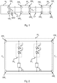
- the printed circuit board / lighting module 20' includes six terminals 200a-200f.
- the positive terminal 100a and the negative terminal 100b representing a ground, enable the reception of a supply signal from an electronic converter 10.
- the positive terminal 100c and the negative terminal 100d may be used for providing said supply signal to another lighting module 20'.
- the positive terminal 100c is connected (within module 20' and e.g. directly via electric traces) to terminal 100a
- the negative terminal 100d is connected (within module 20' and e.g. directly via electric traces) to terminal 100b.
- the terminals 100e and 100f enable a connection in series of a plurality of modules 20', and the operation of said terminals will be described in the following.
- module 20' includes a first LED string 22 a including two LEDs L 1 and L 2 connected in series, and a second LED string 22 b including two LEDs L 3 and L 4 connected in series.
- each lighting module 20' employs a printed circuit board enabling mounting six LEDs L, which may be distributed in strings 22a and 22b.
- said means enable the following connections:
- each LED L 1 , L 2 , L 3 and L 4 has, connected in parallel thereto, a connector having two contacts JP2 1 , JP2 2 , JP2 3 and JP2 4 , which therefore may be closed via a link, thereby bypassing the respective LED L.
- these connectors JP2 may be employed to bypass the connection terminals on a printed circuit board, if the respective LED is not mounted on the printed circuit board.
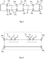
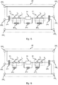
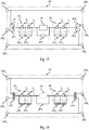
- Figures 7 and 8 show two embodiments of the electric connection of the printed circuit board shown in Figure 6 .
- Module 20' V may therefore be used in the lighting system described with reference to Figure 1 , and the corresponding description is applicable thereto in its entirety.
- the terminals 200e and 200f are unused.
- the presently considered embodiment therefore connects the LEDs L of lighting module 20' C directly between the terminals 200a and 200b.
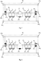
- the first lighting module 20 C1 (specifically the terminals 200a and 200b) is connected to the electronic converter 10 (specifically to the terminals 100a and 100b) by means of a first electric cable 50, having e.g. two wires.
- the second lighting 20 C2 (specifically the terminals 200e and 200b) is connected to the first lighting module 20 V1 (specifically to the terminals 200f and 200d) by means of a first electric cable 52, having e.g. two wires.
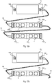
- the means JP2 may be used in order to bypass, i.e. deactivate, one or more of the LEDs L, so that the voltage of the LEDs is lower than the voltage provided by the electronic converter 10 V .
- Figure 16 shows an embodiment wherein some LEDs, e.g. LEDs L 2 and L 4 , are always active, while other LEDs, e.g. LEDs L 1 and L 3 may have respective means JP2 associated thereto.
- step 1004 the corresponding printed circuit board is implemented on the basis of the electric circuit designed in step 1002.
- module 20' is supplied with a regulated current (result "C" of step 1012)
- the corresponding selection means JP3 are set in such a way as to bypass the electric contacts of the current regulator 24.
- step 1028 the means JP4 are set in such a way as to connect the negative terminal of the last string of LEDs 22b to the terminal 200f, e.g. by short-circuiting the connectors / electric contacts JP4 a .
- the method proceeds to the step 1006 for determining the configuration of the next/following lighting module 20' in the chain.
Landscapes
- Engineering & Computer Science (AREA)
- Microelectronics & Electronic Packaging (AREA)
- Manufacturing & Machinery (AREA)
- Circuit Arrangement For Electric Light Sources In General (AREA)
Claims (10)
- Verfahren zum Herstellen einer Vielzahl von Beleuchtungsmodulen (20') einer Beleuchtungsmodulreihe, die ein erstes Beleuchtungsmodul und ein letztes Beleuchtungsmodul beinhaltet, das Verfahren umfassend die Schritte von:- Herstellen (1002, 1004) einer Leiterplatte für jedes Beleuchtungsmodul in der Vielzahl von Beleuchtungsmodulen (20') umfassend:- Metallische Bereiche umfassend:- einen ersten (200a), einen zweiten (200e) und einen dritten positiven Anschluss (200f),
einen ersten (200b) und einen zweiten (200d) negativen Anschluss, wobei der zweite negative Anschluss (200d) mit dem ersten negativen Anschluss (200b) verbunden ist,- elektrische Kontakte zum Anbringen einer Vielzahl von LEDs (L) und elektrische Leiterbahnen zwischen den elektrischen Kontakten, so dass die Vielzahl von LEDs (L) im montierten Zustand in Reihe geschaltet sind und eine LED-Kette (22) mit einem positiven Anschluss und einem negativen Anschluss bilden; und- erste Auswahlmittel (JP1), die mit elektrischen Leiterbahnen und metallischen Kontakten ausgeführt sind, die geeignet sind, über Verbindungen kurzgeschlossen zu werden, wobei die ersten Auswahlmittel (JP1) umfassen:- einen ersten Satz von zwei Kontakten (JP1a), die zwischen dem ersten positiven Anschluss (200a) und dem positiven Anschluss der LED-Kette (22) verbunden sind, und- einen zweiten Satz von zwei Kontakten (JP1b), die zwischen dem zweiten positiven Anschluss (200e) und dem positiven Anschluss der LED-Kette (22) verbunden sind;- zweite Auswahlmittel (JP4), die mit elektrischen Leiterbahnen und metallischen Kontakten ausgeführt sind, die geeignet sind, über Verbindungen kurzgeschlossen zu werden, wobei die zweiten Auswahlmittel (JP4) umfassen:- einen dritten Satz von zwei Kontakten (JP4a), die zwischen dem negativen Anschluss der LED-Kette (22) und dem dritten positiven Anschluss (200f) verbunden sind, und- einen vierten Satz von zwei Kontakten (JP4b), die zwischen dem negativen Anschluss der LED-Kette (22) und dem ersten negativen Anschluss (200b) verbunden sind;- Löten (1006) einer Vielzahl von LEDs (L) auf der Leiterplatte, um die LED-Kette (22) zu bilden;- Bestimmen (1008, 1018) für jedes der Beleuchtungsmodule in der Vielzahl von Beleuchtungsmodulen (20'), ob das Beleuchtungsmodul (20') das erste oder das letzte Beleuchtungsmodul (20') ist, unda) wenn das Beleuchtungsmodul (20') das erste Beleuchtungsmodul ist, Kurzschließen über eine Verbindung des ersten Satzes von zwei Kontakten (JP1a) oder des zweiten Satzes von zwei Kontakten (JP1b) und Kurzschließen über eine Verbindung des dritten Satzes von zwei Kontakten (JP4a), so dass die LED-Kette (22) zwischen dem ersten positiven Anschluss (200a) und dem dritten positiven Anschluss (200f) oder zwischen dem zweiten positiven Anschluss (200e) und dem dritten positiven Anschluss (200f) verbunden ist; undb) wenn das Beleuchtungsmodul (20') das letzte Beleuchtungsmodul ist, Kurzschließen über eine Verbindung des zweiten Satzes von zwei Kontakten (JP1b) und Kurzschließen über eine Verbindung des vierten Satzes von zwei Kontakten (JP4b), so dass die LED-Kette (22) zwischen dem zweiten positiven Anschluss (200e) und dem ersten negativen Anschluss (200b) verbunden ist. - Verfahren nach Anspruch 1, umfassend das Implementieren der beiden Kontakte des ersten (JP1a), zweiten (JP1b), dritten (JP4a) und vierten (JP4b) Satzes jedes der Beleuchtungsmodule in der Vielzahl der Beleuchtungsmodule (20') als metallische Kontakte mit einem SMD-Format 1H/0201, 1E/0402, 1J/0603, 2A/0805 oder 2B/1206.
- Verfahren nach einem der vorhergehenden Ansprüche, umfassend das Implementieren auf der Leiterplatte jedes der Beleuchtungsmodule aus der Vielzahl von Beleuchtungsmodulen (20') eines vierten positiven Anschlusses (200c), der mit dem ersten positiven Anschluss (200a) verbunden ist.
- Verfahren nach einem der vorhergehenden Ansprüche, umfassend das Implementieren auf der Leiterplatte jedes der Beleuchtungsmodule in der Vielzahl von Beleuchtungsmodulen (20') von Umgehungsmitteln (JP2), die mit elektrischen Leiterbahnen und/oder metallischen Kontakten implementiert sind, die ausgelegt sind, um kurzgeschlossen zu werden, um eine oder mehrere der LEDs (L) in der Vielzahl von LEDs (L) selektiv zu umgehen.
- Verfahren nach einem der vorhergehenden Ansprüche, umfassend das Implementieren auf der Leiterplatte von mindestens einem der Beleuchtungsmodule aus der Vielzahl der Beleuchtungsmodule (20'):- elektrische Kontakte für die Montage oder die Implementierung eines Stromreglers (24); und- weitere Umgehungsmittel (JP3), die mit elektrischen Leiterbahnen und/oder metallischen Kontakten implementiert sind, die ausgelegt sind, um kurzgeschlossen zu werden, um den Stromregler (24) selektiv zu umgehen.
- Beleuchtungssystem, umfassend einen elektronischen Wandler (10v; 10c), der ausgelegt ist, um eine geregelte Spannung (Vout) oder einen geregelten Strom (iout) bereitzustellen, und eine Vielzahl von Beleuchtungsmodulen (20'), die ein erstes Beleuchtungsmodul und ein letztes Beleuchtungsmodul beinhalten, wobei jedes der Beleuchtungsmodule in der Vielzahl von Beleuchtungsmodulen (20') eine Leiterplatte umfasst, die metallische Bereiche umfasst, die umfassen:- einen ersten (200a), einen zweiten (200e) und einen dritten positiven Anschluss (200f),Gekennzeichnet dadurch, dass die bedruckte Leiterplatte von jedem der Beleuchtungsmodule in der Vielzahl von Beleuchtungsmodulen (20') umfasst:
einen ersten (200b) und einen zweiten (200d) negativen Anschluss, wobei der zweite negative Anschluss (200d) mit dem ersten negativen Anschluss (200b) verbunden ist,- elektrische Kontakte, wobei eine Vielzahl von LEDs (L) auf den elektrischen Kontakten angebracht ist, und elektrische Leiterbahnen zwischen den elektrischen Kontakten, so dass die Vielzahl von LEDs (L) in Reihe geschaltet sind und eine LED-Kette (22) mit einem positiven Anschluss und einem negativen Anschluss bilden;- erste Auswahlmittel (JP1), die mit elektrischen Leiterbahnen und metallischen Kontakten ausgeführt sind, die geeignet sind, über Verbindungen kurzgeschlossen zu werden, die ersten Auswahlmittel (JP1) umfassend:- einen ersten Satz von zwei Kontakten (JP1a), die zwischen dem ersten positiven Anschluss (200a) und dem positiven Anschluss der LED-Kette (22) verbunden sind, und- einen zweiten Satz von zwei Kontakten (JP1b), die zwischen dem zweiten positiven Anschluss (200e) und dem positiven Anschluss der LED-Kette (22) verbunden sind;- zweite Auswahlmittel (JP4), die mit elektrischen Leiterbahnen und metallischen Kontakten ausgeführt sind, die geeignet sind, über Verbindungen kurzgeschlossen zu werden, die zweiten Auswahlmittel (JP4) umfassend:- einen dritten Satz von zwei Kontakten (JP4a), die zwischen dem negativen Anschluss der LED-Kette (22) und dem dritten positiven Anschluss (200f) verbunden sind, und- einen vierten Satz von zwei Kontakten (JP4b), die zwischen dem negativen Anschluss der LED-Kette (22) und dem ersten negativen Anschluss (200b) verbunden sind;Wobei der erste Satz von zwei Kontakten (JP1a) oder der zweite Satz von zwei Kontakten (JP1b) vom ersten Beleuchtungsmodul über eine Verbindung kurzgeschlossen sind, und der dritte Satz von zwei Kontakten (JP4a) des ersten Beleuchtungsmoduls kurzgeschlossen sind, so dass die LED-Kette (22) des ersten Beleuchtungsmoduls zwischen dem ersten positiven Anschluss (200a) und dem dritten positiven Anschluss (200f) oder zwischen dem zweiten positiven Anschluss (200e) und dem dritten positiven Anschluss (200f) des ersten Beleuchtungsmoduls verbunden ist; und
wobei der zweite Satz von zwei Kontakten (JP1b) und der vierte Satz von zwei Kontakten (JP4b) vom letzten Beleuchtungsmodul über eine jeweilige Verbindung kurzgeschlossen sind, so dass die LED-Kette (22) vom letzten Beleuchtungsmodul zwischen dem zweiten positiven Anschluss (200e) und dem ersten negativen Anschluss (200b) des letzten Beleuchtungsmoduls verbunden ist. - Beleuchtungssystem nach Anspruch 6, wobei die beiden Kontakte des ersten (JP1a), zweiten (JP1b), dritten (JP4a) und vierten (JP4b) Satzes jedes der Beleuchtungsmodule in der Vielzahl der Beleuchtungsmodule (20') metallische Kontakte mit einem SMD-Format 1H/0201, 1E/0402, 1J/0603, 2A/0805 oder 2B/1206 sind.
- Beleuchtungssystem nach Anspruch 6 oder Anspruch 7, wobei die Leiterplatte jedes der Beleuchtungsmodule in der Vielzahl der Beleuchtungsmodule (20') einen vierten positiven Anschluss (200c) umfasst, der mit dem ersten positiven Anschluss (200a) verbunden ist.
- Beleuchtungssystem nach einem der Ansprüche 6 bis 8, wobei die Leiterplatte jedes der Beleuchtungsmodule in der Vielzahl von Beleuchtungsmodulen (20') Umgehungsmittel (JP2) umfasst, die mit elektrischen Leiterbahnen und/oder metallischen Kontakten implementiert sind, die so konfiguriert sind, dass sie kurzgeschlossen sind, um eine oder mehrere der LEDs (L) selektiv zu umgehen.
- Beleuchtungssystem nach einem der Ansprüche 6 bis 9, wobei die Leiterplatte von mindestens einem der Beleuchtungsmodule in der Vielzahl der Beleuchtungsmodule (20') umfasst:- elektrische Kontakte für das Anbringen oder die Implementierung eines Stromreglers (24); und- ein weiteres Umgehungsmittel (JP3), das mit elektrischen Leiterbahnen und/oder metallischen Kontakten implementiert ist, die konfiguriert sind, um kurzgeschlossen zu werden, um den Stromregler (24) selektiv zu umgehen.
Applications Claiming Priority (1)
| Application Number | Priority Date | Filing Date | Title |
|---|---|---|---|
| IT201600125049 | 2016-12-12 |
Publications (2)
| Publication Number | Publication Date |
|---|---|
| EP3334263A1 EP3334263A1 (de) | 2018-06-13 |
| EP3334263B1 true EP3334263B1 (de) | 2019-08-21 |
Family
ID=58545083
Family Applications (1)
| Application Number | Title | Priority Date | Filing Date |
|---|---|---|---|
| EP17205871.1A Active EP3334263B1 (de) | 2016-12-12 | 2017-12-07 | Leiterplatte, entsprechendes beleuchtungsmodul, beleuchtungssystem und verfahren zur implementierung von beleuchtungsmodulen |
Country Status (2)
| Country | Link |
|---|---|
| US (1) | US10356862B2 (de) |
| EP (1) | EP3334263B1 (de) |
Families Citing this family (4)
| Publication number | Priority date | Publication date | Assignee | Title |
|---|---|---|---|---|
| US9468062B2 (en) * | 2013-01-02 | 2016-10-11 | Austin Ip Partners | Light emitting diode light structures |
| PL3715702T3 (pl) | 2019-03-28 | 2023-10-02 | Stepan Engineering Gmbh | Taśma LED na napięcie stale |
| FR3116589B1 (fr) * | 2020-11-23 | 2025-08-15 | Airstar Sas | Dispositif d'éclairage |
| GB2623763A (en) * | 2022-10-24 | 2024-05-01 | Light Science Tech Limited | Controlled environment agriculture lighting assembly, PCB and method |
Family Cites Families (4)
| Publication number | Priority date | Publication date | Assignee | Title |
|---|---|---|---|---|
| JPH0817269B2 (ja) * | 1988-05-11 | 1996-02-21 | 株式会社ソフィアシステムズ | 回路ライター |
| US20080144299A1 (en) * | 2004-07-15 | 2008-06-19 | Redmond Frank E | Systems for and methods of circuit construction |
| US7378600B2 (en) * | 2005-03-14 | 2008-05-27 | Chan Eric K D | Electronic circuit prototyping composite support |
| CN104053943A (zh) | 2012-01-16 | 2014-09-17 | 欧司朗有限公司 | 照明模块 |
-
2017
- 2017-12-07 EP EP17205871.1A patent/EP3334263B1/de active Active
- 2017-12-11 US US15/837,024 patent/US10356862B2/en active Active
Non-Patent Citations (1)
| Title |
|---|
| None * |
Also Published As
| Publication number | Publication date |
|---|---|
| EP3334263A1 (de) | 2018-06-13 |
| US20180168009A1 (en) | 2018-06-14 |
| US10356862B2 (en) | 2019-07-16 |
Similar Documents
| Publication | Publication Date | Title |
|---|---|---|
| EP3334263B1 (de) | Leiterplatte, entsprechendes beleuchtungsmodul, beleuchtungssystem und verfahren zur implementierung von beleuchtungsmodulen | |
| JP5430635B2 (ja) | 一体成形ledライトワイヤ | |
| US8305717B2 (en) | LED modules for sign channel letters and driving circuit | |
| WO2002089222A1 (en) | Light source coupler, illuminant device, patterned conductor, and method for manufcturing light source coupler | |
| JP2013508946A (ja) | Led回路及びアセンブリ | |
| EP2835034B1 (de) | Vorrichtung und verfahren für externe programmierung von led-treiber | |
| US10624168B2 (en) | Programmable light emitting diode luminaire | |
| WO2020178097A1 (en) | Modular led string | |
| JP4449753B2 (ja) | Ledモジュールの製造方法 | |
| US7408305B2 (en) | Codable electronic circuit arrangement and method for producing it | |
| US20200386374A1 (en) | Led string lamp, method of manufacturing the same, and led string lamp system | |
| EP3928030A1 (de) | Led-beleuchtungsanordnung mit integrierter leistungsumwandlung und digitalem sende-empfänger | |
| EP3389341B1 (de) | Leiterplatte einer leuchte und verfahren zur herstellung der leiterplatte einer leuchte | |
| CN109578840B (zh) | 线灯连接方法及线灯连接电路 | |
| CN217816314U (zh) | 一种可在任意位置裁剪的照明电路和灯带 | |
| CN104456475A (zh) | 一种调光装置以及驱动调光装置 | |
| CN204268416U (zh) | 一种调光装置以及驱动调光装置 | |
| WO2022046504A1 (en) | Linear lighting with selectable light output | |
| CN223566286U (zh) | Led显示屏 | |
| CZ308549B6 (cs) | Světelné zařízení vozidla, zejména sdružené světelné zařízení vozidla | |
| EP3358911B1 (de) | Leuchtdiodensystem mit mittels stromleitungen getragenen lichtsignalen | |
| CN223666512U (zh) | Led灯板 | |
| US9022602B2 (en) | Modular multichannel connector system and method | |
| US20250149837A1 (en) | Fused current tap and a cord connector for high voltage direct insert light string | |
| US10117305B2 (en) | Driving system and method for planar organic electroluminescent device |
Legal Events
| Date | Code | Title | Description |
|---|---|---|---|
| PUAI | Public reference made under article 153(3) epc to a published international application that has entered the european phase |
Free format text: ORIGINAL CODE: 0009012 |
|
| STAA | Information on the status of an ep patent application or granted ep patent |
Free format text: STATUS: THE APPLICATION HAS BEEN PUBLISHED |
|
| AK | Designated contracting states |
Kind code of ref document: A1 Designated state(s): AL AT BE BG CH CY CZ DE DK EE ES FI FR GB GR HR HU IE IS IT LI LT LU LV MC MK MT NL NO PL PT RO RS SE SI SK SM TR |
|
| AX | Request for extension of the european patent |
Extension state: BA ME |
|
| STAA | Information on the status of an ep patent application or granted ep patent |
Free format text: STATUS: REQUEST FOR EXAMINATION WAS MADE |
|
| 17P | Request for examination filed |
Effective date: 20181207 |
|
| RBV | Designated contracting states (corrected) |
Designated state(s): AL AT BE BG CH CY CZ DE DK EE ES FI FR GB GR HR HU IE IS IT LI LT LU LV MC MK MT NL NO PL PT RO RS SE SI SK SM TR |
|
| REG | Reference to a national code |
Ref country code: DE Ref legal event code: R079 Ref document number: 602017006352 Country of ref document: DE Free format text: PREVIOUS MAIN CLASS: H05K0013000000 Ipc: H05B0033080000 |
|
| GRAP | Despatch of communication of intention to grant a patent |
Free format text: ORIGINAL CODE: EPIDOSNIGR1 |
|
| STAA | Information on the status of an ep patent application or granted ep patent |
Free format text: STATUS: GRANT OF PATENT IS INTENDED |
|
| RIC1 | Information provided on ipc code assigned before grant |
Ipc: H05K 1/02 20060101ALI20190222BHEP Ipc: H05K 3/22 20060101ALI20190222BHEP Ipc: H05B 33/08 20060101AFI20190222BHEP |
|
| INTG | Intention to grant announced |
Effective date: 20190401 |
|
| GRAS | Grant fee paid |
Free format text: ORIGINAL CODE: EPIDOSNIGR3 |
|
| GRAA | (expected) grant |
Free format text: ORIGINAL CODE: 0009210 |
|
| STAA | Information on the status of an ep patent application or granted ep patent |
Free format text: STATUS: THE PATENT HAS BEEN GRANTED |
|
| AK | Designated contracting states |
Kind code of ref document: B1 Designated state(s): AL AT BE BG CH CY CZ DE DK EE ES FI FR GB GR HR HU IE IS IT LI LT LU LV MC MK MT NL NO PL PT RO RS SE SI SK SM TR |
|
| REG | Reference to a national code |
Ref country code: GB Ref legal event code: FG4D |
|
| REG | Reference to a national code |
Ref country code: CH Ref legal event code: EP |
|
| REG | Reference to a national code |
Ref country code: DE Ref legal event code: R096 Ref document number: 602017006352 Country of ref document: DE |
|
| REG | Reference to a national code |
Ref country code: AT Ref legal event code: REF Ref document number: 1171229 Country of ref document: AT Kind code of ref document: T Effective date: 20190915 |
|
| REG | Reference to a national code |
Ref country code: IE Ref legal event code: FG4D |
|
| REG | Reference to a national code |
Ref country code: DE Ref legal event code: R079 Ref document number: 602017006352 Country of ref document: DE Free format text: PREVIOUS MAIN CLASS: H05B0033080000 Ipc: H05B0045000000 |
|
| REG | Reference to a national code |
Ref country code: LT Ref legal event code: MG4D |
|
| REG | Reference to a national code |
Ref country code: NL Ref legal event code: MP Effective date: 20190821 |
|
| PG25 | Lapsed in a contracting state [announced via postgrant information from national office to epo] |
Ref country code: PT Free format text: LAPSE BECAUSE OF FAILURE TO SUBMIT A TRANSLATION OF THE DESCRIPTION OR TO PAY THE FEE WITHIN THE PRESCRIBED TIME-LIMIT Effective date: 20191223 Ref country code: BG Free format text: LAPSE BECAUSE OF FAILURE TO SUBMIT A TRANSLATION OF THE DESCRIPTION OR TO PAY THE FEE WITHIN THE PRESCRIBED TIME-LIMIT Effective date: 20191121 Ref country code: SE Free format text: LAPSE BECAUSE OF FAILURE TO SUBMIT A TRANSLATION OF THE DESCRIPTION OR TO PAY THE FEE WITHIN THE PRESCRIBED TIME-LIMIT Effective date: 20190821 Ref country code: LT Free format text: LAPSE BECAUSE OF FAILURE TO SUBMIT A TRANSLATION OF THE DESCRIPTION OR TO PAY THE FEE WITHIN THE PRESCRIBED TIME-LIMIT Effective date: 20190821 Ref country code: NL Free format text: LAPSE BECAUSE OF FAILURE TO SUBMIT A TRANSLATION OF THE DESCRIPTION OR TO PAY THE FEE WITHIN THE PRESCRIBED TIME-LIMIT Effective date: 20190821 Ref country code: HR Free format text: LAPSE BECAUSE OF FAILURE TO SUBMIT A TRANSLATION OF THE DESCRIPTION OR TO PAY THE FEE WITHIN THE PRESCRIBED TIME-LIMIT Effective date: 20190821 Ref country code: FI Free format text: LAPSE BECAUSE OF FAILURE TO SUBMIT A TRANSLATION OF THE DESCRIPTION OR TO PAY THE FEE WITHIN THE PRESCRIBED TIME-LIMIT Effective date: 20190821 Ref country code: NO Free format text: LAPSE BECAUSE OF FAILURE TO SUBMIT A TRANSLATION OF THE DESCRIPTION OR TO PAY THE FEE WITHIN THE PRESCRIBED TIME-LIMIT Effective date: 20191121 |
|
| PG25 | Lapsed in a contracting state [announced via postgrant information from national office to epo] |
Ref country code: AL Free format text: LAPSE BECAUSE OF FAILURE TO SUBMIT A TRANSLATION OF THE DESCRIPTION OR TO PAY THE FEE WITHIN THE PRESCRIBED TIME-LIMIT Effective date: 20190821 Ref country code: ES Free format text: LAPSE BECAUSE OF FAILURE TO SUBMIT A TRANSLATION OF THE DESCRIPTION OR TO PAY THE FEE WITHIN THE PRESCRIBED TIME-LIMIT Effective date: 20190821 Ref country code: GR Free format text: LAPSE BECAUSE OF FAILURE TO SUBMIT A TRANSLATION OF THE DESCRIPTION OR TO PAY THE FEE WITHIN THE PRESCRIBED TIME-LIMIT Effective date: 20191122 Ref country code: IS Free format text: LAPSE BECAUSE OF FAILURE TO SUBMIT A TRANSLATION OF THE DESCRIPTION OR TO PAY THE FEE WITHIN THE PRESCRIBED TIME-LIMIT Effective date: 20191221 Ref country code: RS Free format text: LAPSE BECAUSE OF FAILURE TO SUBMIT A TRANSLATION OF THE DESCRIPTION OR TO PAY THE FEE WITHIN THE PRESCRIBED TIME-LIMIT Effective date: 20190821 Ref country code: LV Free format text: LAPSE BECAUSE OF FAILURE TO SUBMIT A TRANSLATION OF THE DESCRIPTION OR TO PAY THE FEE WITHIN THE PRESCRIBED TIME-LIMIT Effective date: 20190821 |
|
| REG | Reference to a national code |
Ref country code: AT Ref legal event code: MK05 Ref document number: 1171229 Country of ref document: AT Kind code of ref document: T Effective date: 20190821 |
|
| PG25 | Lapsed in a contracting state [announced via postgrant information from national office to epo] |
Ref country code: TR Free format text: LAPSE BECAUSE OF FAILURE TO SUBMIT A TRANSLATION OF THE DESCRIPTION OR TO PAY THE FEE WITHIN THE PRESCRIBED TIME-LIMIT Effective date: 20190821 |
|
| PG25 | Lapsed in a contracting state [announced via postgrant information from national office to epo] |
Ref country code: RO Free format text: LAPSE BECAUSE OF FAILURE TO SUBMIT A TRANSLATION OF THE DESCRIPTION OR TO PAY THE FEE WITHIN THE PRESCRIBED TIME-LIMIT Effective date: 20190821 Ref country code: IT Free format text: LAPSE BECAUSE OF FAILURE TO SUBMIT A TRANSLATION OF THE DESCRIPTION OR TO PAY THE FEE WITHIN THE PRESCRIBED TIME-LIMIT Effective date: 20190821 Ref country code: AT Free format text: LAPSE BECAUSE OF FAILURE TO SUBMIT A TRANSLATION OF THE DESCRIPTION OR TO PAY THE FEE WITHIN THE PRESCRIBED TIME-LIMIT Effective date: 20190821 Ref country code: EE Free format text: LAPSE BECAUSE OF FAILURE TO SUBMIT A TRANSLATION OF THE DESCRIPTION OR TO PAY THE FEE WITHIN THE PRESCRIBED TIME-LIMIT Effective date: 20190821 Ref country code: PL Free format text: LAPSE BECAUSE OF FAILURE TO SUBMIT A TRANSLATION OF THE DESCRIPTION OR TO PAY THE FEE WITHIN THE PRESCRIBED TIME-LIMIT Effective date: 20190821 Ref country code: DK Free format text: LAPSE BECAUSE OF FAILURE TO SUBMIT A TRANSLATION OF THE DESCRIPTION OR TO PAY THE FEE WITHIN THE PRESCRIBED TIME-LIMIT Effective date: 20190821 |
|
| PG25 | Lapsed in a contracting state [announced via postgrant information from national office to epo] |
Ref country code: IS Free format text: LAPSE BECAUSE OF FAILURE TO SUBMIT A TRANSLATION OF THE DESCRIPTION OR TO PAY THE FEE WITHIN THE PRESCRIBED TIME-LIMIT Effective date: 20200224 Ref country code: SK Free format text: LAPSE BECAUSE OF FAILURE TO SUBMIT A TRANSLATION OF THE DESCRIPTION OR TO PAY THE FEE WITHIN THE PRESCRIBED TIME-LIMIT Effective date: 20190821 Ref country code: SM Free format text: LAPSE BECAUSE OF FAILURE TO SUBMIT A TRANSLATION OF THE DESCRIPTION OR TO PAY THE FEE WITHIN THE PRESCRIBED TIME-LIMIT Effective date: 20190821 Ref country code: CZ Free format text: LAPSE BECAUSE OF FAILURE TO SUBMIT A TRANSLATION OF THE DESCRIPTION OR TO PAY THE FEE WITHIN THE PRESCRIBED TIME-LIMIT Effective date: 20190821 |
|
| REG | Reference to a national code |
Ref country code: DE Ref legal event code: R097 Ref document number: 602017006352 Country of ref document: DE |
|
| PLBE | No opposition filed within time limit |
Free format text: ORIGINAL CODE: 0009261 |
|
| STAA | Information on the status of an ep patent application or granted ep patent |
Free format text: STATUS: NO OPPOSITION FILED WITHIN TIME LIMIT |
|
| PG2D | Information on lapse in contracting state deleted |
Ref country code: IS |
|
| 26N | No opposition filed |
Effective date: 20200603 |
|
| REG | Reference to a national code |
Ref country code: BE Ref legal event code: MM Effective date: 20191231 |
|
| PG25 | Lapsed in a contracting state [announced via postgrant information from national office to epo] |
Ref country code: MC Free format text: LAPSE BECAUSE OF FAILURE TO SUBMIT A TRANSLATION OF THE DESCRIPTION OR TO PAY THE FEE WITHIN THE PRESCRIBED TIME-LIMIT Effective date: 20190821 Ref country code: SI Free format text: LAPSE BECAUSE OF FAILURE TO SUBMIT A TRANSLATION OF THE DESCRIPTION OR TO PAY THE FEE WITHIN THE PRESCRIBED TIME-LIMIT Effective date: 20190821 |
|
| PG25 | Lapsed in a contracting state [announced via postgrant information from national office to epo] |
Ref country code: FR Free format text: LAPSE BECAUSE OF NON-PAYMENT OF DUE FEES Effective date: 20191231 Ref country code: LU Free format text: LAPSE BECAUSE OF NON-PAYMENT OF DUE FEES Effective date: 20191207 Ref country code: IE Free format text: LAPSE BECAUSE OF NON-PAYMENT OF DUE FEES Effective date: 20191207 |
|
| PG25 | Lapsed in a contracting state [announced via postgrant information from national office to epo] |
Ref country code: BE Free format text: LAPSE BECAUSE OF NON-PAYMENT OF DUE FEES Effective date: 20191231 |
|
| PG25 | Lapsed in a contracting state [announced via postgrant information from national office to epo] |
Ref country code: CY Free format text: LAPSE BECAUSE OF FAILURE TO SUBMIT A TRANSLATION OF THE DESCRIPTION OR TO PAY THE FEE WITHIN THE PRESCRIBED TIME-LIMIT Effective date: 20190821 |
|
| PG25 | Lapsed in a contracting state [announced via postgrant information from national office to epo] |
Ref country code: HU Free format text: LAPSE BECAUSE OF FAILURE TO SUBMIT A TRANSLATION OF THE DESCRIPTION OR TO PAY THE FEE WITHIN THE PRESCRIBED TIME-LIMIT; INVALID AB INITIO Effective date: 20171207 Ref country code: MT Free format text: LAPSE BECAUSE OF FAILURE TO SUBMIT A TRANSLATION OF THE DESCRIPTION OR TO PAY THE FEE WITHIN THE PRESCRIBED TIME-LIMIT Effective date: 20190821 |
|
| REG | Reference to a national code |
Ref country code: CH Ref legal event code: PL |
|
| PG25 | Lapsed in a contracting state [announced via postgrant information from national office to epo] |
Ref country code: CH Free format text: LAPSE BECAUSE OF NON-PAYMENT OF DUE FEES Effective date: 20201231 Ref country code: LI Free format text: LAPSE BECAUSE OF NON-PAYMENT OF DUE FEES Effective date: 20201231 |
|
| PG25 | Lapsed in a contracting state [announced via postgrant information from national office to epo] |
Ref country code: MK Free format text: LAPSE BECAUSE OF FAILURE TO SUBMIT A TRANSLATION OF THE DESCRIPTION OR TO PAY THE FEE WITHIN THE PRESCRIBED TIME-LIMIT Effective date: 20190821 |
|
| GBPC | Gb: european patent ceased through non-payment of renewal fee |
Effective date: 20211207 |
|
| PG25 | Lapsed in a contracting state [announced via postgrant information from national office to epo] |
Ref country code: GB Free format text: LAPSE BECAUSE OF NON-PAYMENT OF DUE FEES Effective date: 20211207 |
|
| REG | Reference to a national code |
Ref country code: DE Ref legal event code: R081 Ref document number: 602017006352 Country of ref document: DE Owner name: OPTOTRONIC GMBH, DE Free format text: FORMER OWNER: OSRAM GMBH, 80807 MUENCHEN, DE Ref country code: DE Ref legal event code: R081 Ref document number: 602017006352 Country of ref document: DE Owner name: INVENTRONICS GMBH, DE Free format text: FORMER OWNER: OSRAM GMBH, 80807 MUENCHEN, DE |
|
| REG | Reference to a national code |
Ref country code: DE Ref legal event code: R081 Ref document number: 602017006352 Country of ref document: DE Owner name: INVENTRONICS GMBH, DE Free format text: FORMER OWNER: OPTOTRONIC GMBH, 85748 GARCHING, DE |
|
| PGFP | Annual fee paid to national office [announced via postgrant information from national office to epo] |
Ref country code: DE Payment date: 20251222 Year of fee payment: 9 |