EP3334184A1 - Acoustic sensor and capacitive transducer - Google Patents
Acoustic sensor and capacitive transducer Download PDFInfo
- Publication number
- EP3334184A1 EP3334184A1 EP17198739.9A EP17198739A EP3334184A1 EP 3334184 A1 EP3334184 A1 EP 3334184A1 EP 17198739 A EP17198739 A EP 17198739A EP 3334184 A1 EP3334184 A1 EP 3334184A1
- Authority
- EP
- European Patent Office
- Prior art keywords
- electrode film
- back plate
- vibration electrode
- vibration
- semiconductor substrate
- Prior art date
- Legal status (The legal status is an assumption and is not a legal conclusion. Google has not performed a legal analysis and makes no representation as to the accuracy of the status listed.)
- Granted
Links
- 239000000758 substrate Substances 0.000 claims abstract description 122
- 230000009466 transformation Effects 0.000 claims abstract description 18
- 239000004065 semiconductor Substances 0.000 claims description 87
- 239000012530 fluid Substances 0.000 claims description 16
- 241000276425 Xiphophorus maculatus Species 0.000 claims description 9
- 230000008859 change Effects 0.000 claims description 6
- 239000011800 void material Substances 0.000 claims description 6
- 238000000034 method Methods 0.000 abstract description 17
- 239000010408 film Substances 0.000 description 295
- XUIMIQQOPSSXEZ-UHFFFAOYSA-N Silicon Chemical compound [Si] XUIMIQQOPSSXEZ-UHFFFAOYSA-N 0.000 description 8
- 229910052710 silicon Inorganic materials 0.000 description 8
- 239000010703 silicon Substances 0.000 description 8
- 230000005764 inhibitory process Effects 0.000 description 4
- 238000006073 displacement reaction Methods 0.000 description 3
- 239000012528 membrane Substances 0.000 description 3
- 230000008569 process Effects 0.000 description 3
- 230000005653 Brownian motion process Effects 0.000 description 2
- 238000005537 brownian motion Methods 0.000 description 2
- 238000004519 manufacturing process Methods 0.000 description 2
- 230000002093 peripheral effect Effects 0.000 description 2
- 230000001131 transforming effect Effects 0.000 description 2
- 230000001133 acceleration Effects 0.000 description 1
- 230000000903 blocking effect Effects 0.000 description 1
- 239000003990 capacitor Substances 0.000 description 1
- 238000006243 chemical reaction Methods 0.000 description 1
- 239000012141 concentrate Substances 0.000 description 1
- 238000005520 cutting process Methods 0.000 description 1
- 230000003247 decreasing effect Effects 0.000 description 1
- 230000006866 deterioration Effects 0.000 description 1
- 238000010030 laminating Methods 0.000 description 1
- 229910021421 monocrystalline silicon Inorganic materials 0.000 description 1
- 230000002265 prevention Effects 0.000 description 1
- 230000009467 reduction Effects 0.000 description 1
- 230000035945 sensitivity Effects 0.000 description 1
- 238000005549 size reduction Methods 0.000 description 1
- 239000010409 thin film Substances 0.000 description 1
Images


Classifications
-
- H—ELECTRICITY
- H04—ELECTRIC COMMUNICATION TECHNIQUE
- H04R—LOUDSPEAKERS, MICROPHONES, GRAMOPHONE PICK-UPS OR LIKE ACOUSTIC ELECTROMECHANICAL TRANSDUCERS; DEAF-AID SETS; PUBLIC ADDRESS SYSTEMS
- H04R19/00—Electrostatic transducers
- H04R19/005—Electrostatic transducers using semiconductor materials
-
- H—ELECTRICITY
- H04—ELECTRIC COMMUNICATION TECHNIQUE
- H04R—LOUDSPEAKERS, MICROPHONES, GRAMOPHONE PICK-UPS OR LIKE ACOUSTIC ELECTROMECHANICAL TRANSDUCERS; DEAF-AID SETS; PUBLIC ADDRESS SYSTEMS
- H04R19/00—Electrostatic transducers
- H04R19/04—Microphones
-
- H—ELECTRICITY
- H04—ELECTRIC COMMUNICATION TECHNIQUE
- H04R—LOUDSPEAKERS, MICROPHONES, GRAMOPHONE PICK-UPS OR LIKE ACOUSTIC ELECTROMECHANICAL TRANSDUCERS; DEAF-AID SETS; PUBLIC ADDRESS SYSTEMS
- H04R9/00—Transducers of moving-coil, moving-strip, or moving-wire type
- H04R9/08—Microphones
-
- B—PERFORMING OPERATIONS; TRANSPORTING
- B81—MICROSTRUCTURAL TECHNOLOGY
- B81B—MICROSTRUCTURAL DEVICES OR SYSTEMS, e.g. MICROMECHANICAL DEVICES
- B81B3/00—Devices comprising flexible or deformable elements, e.g. comprising elastic tongues or membranes
- B81B3/0064—Constitution or structural means for improving or controlling the physical properties of a device
- B81B3/0067—Mechanical properties
- B81B3/0072—For controlling internal stress or strain in moving or flexible elements, e.g. stress compensating layers
-
- H—ELECTRICITY
- H04—ELECTRIC COMMUNICATION TECHNIQUE
- H04R—LOUDSPEAKERS, MICROPHONES, GRAMOPHONE PICK-UPS OR LIKE ACOUSTIC ELECTROMECHANICAL TRANSDUCERS; DEAF-AID SETS; PUBLIC ADDRESS SYSTEMS
- H04R19/00—Electrostatic transducers
- H04R19/01—Electrostatic transducers characterised by the use of electrets
-
- B—PERFORMING OPERATIONS; TRANSPORTING
- B81—MICROSTRUCTURAL TECHNOLOGY
- B81B—MICROSTRUCTURAL DEVICES OR SYSTEMS, e.g. MICROMECHANICAL DEVICES
- B81B2201/00—Specific applications of microelectromechanical systems
- B81B2201/02—Sensors
- B81B2201/0257—Microphones or microspeakers
-
- B—PERFORMING OPERATIONS; TRANSPORTING
- B81—MICROSTRUCTURAL TECHNOLOGY
- B81B—MICROSTRUCTURAL DEVICES OR SYSTEMS, e.g. MICROMECHANICAL DEVICES
- B81B3/00—Devices comprising flexible or deformable elements, e.g. comprising elastic tongues or membranes
- B81B3/0018—Structures acting upon the moving or flexible element for transforming energy into mechanical movement or vice versa, i.e. actuators, sensors, generators
- B81B3/0021—Transducers for transforming electrical into mechanical energy or vice versa
-
- H—ELECTRICITY
- H04—ELECTRIC COMMUNICATION TECHNIQUE
- H04R—LOUDSPEAKERS, MICROPHONES, GRAMOPHONE PICK-UPS OR LIKE ACOUSTIC ELECTROMECHANICAL TRANSDUCERS; DEAF-AID SETS; PUBLIC ADDRESS SYSTEMS
- H04R1/00—Details of transducers, loudspeakers or microphones
- H04R1/20—Arrangements for obtaining desired frequency or directional characteristics
- H04R1/22—Arrangements for obtaining desired frequency or directional characteristics for obtaining desired frequency characteristic only
- H04R1/28—Transducer mountings or enclosures modified by provision of mechanical or acoustic impedances, e.g. resonator, damping means
- H04R1/2807—Enclosures comprising vibrating or resonating arrangements
- H04R1/2815—Enclosures comprising vibrating or resonating arrangements of the bass reflex type
- H04R1/2823—Vents, i.e. ports, e.g. shape thereof or tuning thereof with damping material
-
- H—ELECTRICITY
- H04—ELECTRIC COMMUNICATION TECHNIQUE
- H04R—LOUDSPEAKERS, MICROPHONES, GRAMOPHONE PICK-UPS OR LIKE ACOUSTIC ELECTROMECHANICAL TRANSDUCERS; DEAF-AID SETS; PUBLIC ADDRESS SYSTEMS
- H04R19/00—Electrostatic transducers
-
- H—ELECTRICITY
- H04—ELECTRIC COMMUNICATION TECHNIQUE
- H04R—LOUDSPEAKERS, MICROPHONES, GRAMOPHONE PICK-UPS OR LIKE ACOUSTIC ELECTROMECHANICAL TRANSDUCERS; DEAF-AID SETS; PUBLIC ADDRESS SYSTEMS
- H04R2201/00—Details of transducers, loudspeakers or microphones covered by H04R1/00 but not provided for in any of its subgroups
- H04R2201/003—Mems transducers or their use
Definitions
- the present invention relates to an acoustic sensor where a capacitive transducer is housed in a casing, and the capacitive transducer in the acoustic sensor. More specifically, the present invention relates to an acoustic sensor where a capacitive transducer is housed in a casing, the capacitive transducer being configured in a capacitor structure formed by the MEMS technique and including a vibration electrode film and a back plate. Further, the present invention relates to the capacitive transducer.
- an ECM Electronic Condenser Microphone
- MEMS Micro Electro Mechanical Systems
- Some of the acoustic sensors as described above house a capacitive transducer having achieved a figuration by using the MEMS technique, the figuration being where a vibration electrode film that vibrates under pressure is disposed facing a back plate fixed with the electrode film via a void.
- the figuration of the capacitive transducer as thus described can be achieved, for example, by the following step: forming on a silicon substrate a vibration electrode film and such a sacrifice layer as to cover the vibration electrode; forming a back plate on the sacrifice layer; and removing the sacrifice layer.
- the capacitive transducer prepared by using the MEMS technique is made up of the vibration electrode film and the back plate having been reduced in thickness, the vibration electrode film is liable to be greatly transformed and damaged when excessive pressure acts thereon, or in some other case.
- Such disadvantage may occur, for example, in a case where large sound pressure is applied into a casing (package) having a pressure hole while the capacitive transducer is housed in the casing. It may also occur in a case where air is blown to the pressure hole of the casing in a package process, or in a case where the capacitive transducer in the state of being housed in the casing falls. This also applies to a case where large sound pressure is applied or air is blown to a mobile electronic device such as a smart phone which includes the capacitive transducer in the state of being housed in the casing, or a case where the device is dropped.
- the vibration electrode film when compressed air flows in from the pressure hole that brings air into the capacitive transducer due to collision by falling or the use of an air gun, the vibration electrode film is greatly transformed to the back plate side (opposite the pressure hole) or the substrate side (at this point, the vibration electrode film may be damaged by coming into contact with the back plate or the substrate).
- the air having entered the capacitive transducer from the pressure hole passes through a gap between the vibration electrode film and the semiconductor substrate or the back plate and/or an opening of the semiconductor substrate or a sound hole of the back plate and gets more deeply into the casing, while transforming the vibration electrode film, to increase the pressure in the casing.
- the pressure in the casing may cause excessive transformation of the vibration electrode film to the pressure hole side and damage on the vibration electrode film.
- the present invention has been made in view of such circumstances as above, and is to particularly prevent internal pressure of a casing that houses a capacitive transducers from increasing due to compressed air flown in from a pressure hole of an acoustic sensor, and to prevent a vibration electrode film from being damaged by being excessively transformed to the pressure hole side caused by the pressure. That is, an object of the present invention is to provide a technique by which, when excessive pressure acts on an acoustic sensor, an increase in pressure in a casing is prevented to suppress excessive transformation of a vibration electrode film of a capacitive transducer caused by the increased pressure.
- an acoustic sensor including: a semiconductor substrate having an opening; a back plate disposed so as to face the opening of the semiconductor substrate, configured to function as a fixed electrode, and having sound holes that allow passage of air; a vibration electrode film disposed so as to face the back plate through a void; and a casing configured to house the substrate, the back plate, and the vibration electrode film, and having a pressure hole that allows inflow of air, the acoustic sensor converting transformation of the vibration electrode film into a change in capacitance between the vibration electrode film and the back plate to detect sound pressure.
- a flow path is formed, which includes any of the sound hole of the back plate, a gap between the back plate and the vibration electrode film, a gap between the vibration electrode film and the semiconductor substrate, and the opening of the semiconductor substrate, and in which a fluid having flown into the casing from the pressure hole moves to a space opposite the pressure hole in the casing across the vibration electrode film, and a flow path cutoff part is further provided, being configured to cut off at least a part of the flow path when the vibration electrode film is transformed to come close to the semiconductor substrate or the back plate due to the fluid flowing into the casing from the pressure hole.
- the air having entered the casing of the acoustic sensor from the pressure hole passes through the gap between the vibration electrode film and the semiconductor substrate or the back plate and/or the opening of the semiconductor substrate or the sound hole of the back plate and gets more deeply into the casing, while transforming the vibration electrode film of the capacitive transducer housed in the casing, to increase the pressure, especially in a region opposite the pressure hole across the vibration electrode film in the casing. Then, the vibration electrode film is excessively transformed to the pressure hole side caused by the increased pressure in the casing.
- a flow path is formed, which includes any of the sound hole of the back plate, the gap between the back plate and the vibration electrode film, the gap between the vibration electrode film and the semiconductor substrate, and the opening of the semiconductor substrate, and in which a fluid having flown in from the pressure hole to the casing moves to a space opposite the pressure hole across the vibration electrode film in the casing, and a flow path cutoff part is further provided, being configured to cut off at least a part of the flow path when the vibration electrode film is transformed to come close to the semiconductor substrate or the back plate due to the fluid flowing into the casing from the pressure hole.
- the present invention when excessive pressure acts on the acoustic sensor, it is possible to prevent passage of the air through the gap between the vibration electrode film and the semiconductor substrate or the back plate of the capacitive transducer housed in the casing and/or the opening of the semiconductor substrate or the sound hole of the back plate to suppress the increase in the pressure especially in a region opposite the pressure hole across the vibration electrode film in the casing, and to suppress excessive transformation of the vibration electrode film caused by the pressure. It is thereby possible to prevent damage on the vibration electrode film when excessive pressure acts on the acoustic sensor.
- the meaning of cutting off includes the case of leaving a part of passage of the fluid, in addition to the case of completely blocking passage of the fluid.
- the flow path cutoff part may be a projection provided in one of the vibration electrode film and the back plate, and configured to block each of at least some of the sound holes in the back plate by abutting with the other of the vibration electrode film and the back plate when the vibration electrode film is transformed to come close to the back plate.
- the vibration electrode film in the capacitive transducer is greatly transformed not to the semiconductor substrate side, but to the back plate side.
- the air passes through the gap between the vibration electrode film and the back plate and/or the sound hole of the back plate and gets more deeply into the casing to increase the pressure in the casing.
- the vibration electrode film transforms and comes close to the back plate, the projection provided in the back plate abuts with the vibration electrode film to block each of at least some of the sound holes in the back plate.
- the projection may block each of the sound holes all over the back plate. According to this, when excessive pressure acts on the acoustic sensor, it is possible to more reliably prevent the air from passing through the sound hole of the back plate in the capacitive transducer and getting more deeply into the casing to suppress the increase in the pressure in the casing.
- the vibration electrode film may be formed including a platy vibration part on which pressure acts, and a fixed part configured to fix the vibration part to the semiconductor substrate, and the projection may block the sound hole disposed in a portion in the back plate, the portion facing an outer periphery of the vibration part of the vibration electrode film.
- the projection by causing the projection to block the sound hole disposed in the portion in the back plate, the portion facing the outer periphery of the vibration part of the vibration electrode film, it is possible to prevent passage of the air through the sound hole disposed in the vicinity of the outer periphery of the vibration part of the vibration electrode film, and to prevent the flow of the air toward the center of the gap between the vibration electrode film and the back plate. It is thereby possible to more efficiently prevent passage of the air through the sound holes all over the back plate, and more efficiently prevent an increase in the pressure in the casing, and damage on the vibration electrode film caused by the pressure.
- the projection may have a cylindrical shape enclosing the sound hole in the back plate in a plan view. According to this, when the vibration electrode film is transformed to come close to the back plate, each of the sound holes in the back plate are surrounded by each of the cylindrical projections and the vibration electrode film, thus making it possible to more reliably block the sound holes. As a result, when excessive pressure acts on the acoustic sensor, it is possible to more reliably prevent the air from passing through the sound hole of the back plate and getting more deeply into the casing to suppress the increase in the pressure in the casing.
- the vibration electrode film may be formed including a platy vibration part on which pressure acts, and a fixed part configured to fix the vibration part to the semiconductor substrate or the back plate
- the flow path cutoff part may be a wall provided in one of the vibration electrode film and the back plate, and formed so as to surround at least a part of the vibration part in the vibration electrode film or surround at least a portion in the back plate, the portion facing a part of the vibration part of the vibration electrode film, and when the vibration electrode film is transformed to come close to the back plate, the flow path cutoff part abuts with the other of the vibration electrode film and the back plate to block up at least a part of a flow path for air that passes through the gap between the vibration electrode film and the back plate and/or the sound hole of the back plate.
- the projection does not block each of the sound holes in the back plate, but the wall formed so as to surround at least a portion in the back plate, in which the portion faces a part of the vibration part of the vibration electrode film, blocks all or at least some of the sound holes in the back plate. It is thus possible to more efficiently cut off the flow path for the air (inhibit the flow of the air) passing through the sound hole of the back plate. At the same time, it is possible to more efficiently cut off the flow path for the air passing through the gap between the vibration electrode film and the back plate.
- the back plate may be provided with a fixed electrode film and the flow path cutoff part, and the fixed electrode film may be provided only in a portion other than a tip of the flow path cutoff part in the back plate. That is, not forming the fixed electrode film at the tip of the flow path cutoff part (e.g., the projection or the wall described above) can prevent occurrence of an electrical short circuit when the flow path cutoff part abuts with the back plate, the semiconductor substrate, the vibration electrode film, or the like.
- the fixed electrode film may be provided only in a portion other than a tip of the flow path cutoff part in the back plate. That is, not forming the fixed electrode film at the tip of the flow path cutoff part (e.g., the projection or the wall described above) can prevent occurrence of an electrical short circuit when the flow path cutoff part abuts with the back plate, the semiconductor substrate, the vibration electrode film, or the like.
- a stopper may further be provided in one of the fixed electrode film and the back plate, the stopper being configured to abut with the other of the fixed electrode film and the back plate when the fixed electrode film and the stopper come close to each other, and the flow path cutoff part may be set as high as or higher than the stopper.
- the flow path cutoff part provided in the vibration electrode film or the back plate can be made higher than the stopper configured to prevent sticking between the vibration electrode film and the back plate when those come close to each other. It is thereby possible to avoid the stopper preventing the flow path cutoff part from abutting with the vibration electrode film or the back plate. Therefore, when excessive pressure acts on the acoustic sensor, it is possible to more reliably prevent an increase in the pressure in the casing and to suppress excessive transformation of the vibration electrode film caused by the above pressure, and to prevent damage on the vibration electrode film at that time.
- the vibration electrode film may be formed including a platy vibration part on which pressure acts, and a fixed part configured to fix the vibration part to the semiconductor substrate or the back plate
- the flow path cutoff part may be a wall provided in one of the vibration electrode film and the semiconductor substrate, and formed so as to surround at least the opening in the semiconductor substrate, or surround at least a portion in the vibration electrode film, the portion facing the opening of the semiconductor substrate, and abuts with the other of the vibration electrode film and the semiconductor substrate to cut off at least a part of a flow path for air that passes through the gap between the vibration electrode film and the semiconductor substrate and/or the opening of the semiconductor substrate when the vibration electrode film is transformed to come close to the semiconductor substrate.
- the wall as the flow path cutoff part is provided in one of the vibration electrode film and the semiconductor substrate, and formed so as to surround at least the opening in the semiconductor substrate or to surround at least a portion in the vibration electrode film, the portion facing the opening of the semiconductor substrate.
- the stopper is further provided in one of the vibration electrode film and the semiconductor substrate, the stopper being configured to abut with the other of the vibration electrode film and the semiconductor substrate when the vibration electrode film and the semiconductor substrate come close to each other, and the wall is made as high as or higher than the stopper. It is thereby possible to avoid the stopper preventing the flow path cutoff part from abutting with the vibration electrode film or the back plate.
- one aspect of the present invention is an acoustic sensor including: a semiconductor substrate having an opening; a back plate disposed so as to face the opening of the semiconductor substrate, and having sound holes that allow passage of air; a vibration electrode film disposed so as to face the back plate through a void; and a casing configured to house the substrate, the back plate, and the vibration electrode film, and having a pressure hole that allows inflow of air, the acoustic sensor converting transformation of the vibration electrode film into a change in capacitance between the vibration electrode film and the back plate to detect sound pressure.
- a flow path inhibition part may further be provided, being configured to inhibit a flow of a fluid that passes through the opening of the semiconductor substrate or the sound hole of the back plate when the vibration electrode film is transformed to come close to the semiconductor substrate or the back plate.
- one aspect of the present invention is a capacitive transducer which is used by being housed in a casing having a pressure hole that allows inflow of air, the capacitive transducer including: a semiconductor substrate having an opening; a back plate disposed so as to face the opening of the semiconductor substrate, configured to function as a fixed electrode, and having sound holes that allow passage of air; and a vibration electrode film disposed so as to face the back plate through a void.
- transformation of the vibration electrode film may be converted into a change in capacitance between the vibration electrode film and the back plate, and a flow path cutoff part may further be provided, being configured to cut off at least a part of a flow path for a fluid that passes through a gap between the vibration electrode film and the semiconductor substrate or the back plate and/or a flow path for a fluid that passes through the opening of the semiconductor substrate or the sound hole of the back plate when the vibration electrode film is transformed to come close to the semiconductor substrate or the back plate.
- the capacitive transducer in the present invention in a case where the capacitive transducer is housed in the casing and used as the acoustic sensor, when excessive pressure acts on the acoustic sensor, it is possible to prevent the air from passing through the gap between the vibration electrode film and the semiconductor substrate or the back plate of the capacitive transducer housed in the casing and/or the opening of the semiconductor substrate or the sound hole of the back plate to suppress the increase in the pressure especially in a region opposite the pressure hole across the vibration electrode film in the casing, and to suppress excessive transformation of the vibration electrode film caused by the pressure. It is thereby possible to prevent damage on the vibration electrode film of the capacitive transducer when excessive pressure acts on the acoustic sensor.
- the flow path cutoff part may be a projection provided in one of the vibration electrode film and the back plate, and configured to block each of at least some of the sound holes in the back plate by abutting with the other of the vibration electrode film and the back plate when the vibration electrode film is transformed to come close to the back plate.
- the projection may block each of the sound holes all over the back plate.
- the vibration electrode film may be formed including a platy vibration part on which pressure acts, and a fixed part configured to fix the vibration part to the semiconductor substrate or the back plate, and the projection may block the sound hole disposed in a portion in the back plate, the portion facing an outer periphery of the vibration part of the vibration electrode film.
- the projection has a cylindrical shape enclosing the sound hole in the back plate in a plan view.
- the vibration electrode film may be formed including a platy vibration part on which pressure acts, and a fixed part configured to fix the vibration part to the semiconductor substrate or the back plate
- the flow path cutoff part may be a wall provided in one of the vibration electrode film and the back plate, and formed so as to surround at least a part of the vibration part in the vibration electrode film or to surround at least a portion in the back plate, the portion facing a part of the vibration part of the vibration electrode film, and abuts with the other of the vibration electrode film and the back plate to cut off at least a part of a flow path for air that passes through the gap between the vibration electrode film and the back plate and/or the sound hole of the back plate when the vibration electrode film is transformed to come close to the back plate.
- the back plate may be provided with a fixed electrode film and the flow path cutoff part, and the fixed electrode film may be provided only in a portion other than a tip of the flow path cutoff part in the back plate.
- a stopper may further be provided in one of the vibration electrode film and the back plate, the stopper being configured to abut with the other of the vibration electrode film and the back plate when the vibration electrode film and the back plate come close to each other, and the flow path cutoff part may be set as high as or higher than the stopper.
- the vibration electrode film may be formed including a platy vibration part on which pressure acts, and a fixed part configured to fix the vibration part to the semiconductor substrate or the back plate
- the flow path cutoff part may be a wall provided in one of the vibration electrode film and the semiconductor substrate, and formed so as to surround at least the opening in the semiconductor substrate, or to surround at least a portion in the vibration electrode film, the portion facing the opening of the semiconductor substrate, and abuts with the other of the vibration electrode film and the semiconductor substrate to cut off at least a part of a flow path for air that passes through the gap between the vibration electrode film and the semiconductor substrate and/or the opening of the semiconductor substrate when the vibration electrode film is transformed to come close to the semiconductor substrate.
- a stopper may further be provided in one of the vibration electrode film and the semiconductor substrate, the stopper being configured to abut with the other of the vibration electrode film and the semiconductor substrate when the vibration electrode film and the semiconductor substrate come close to each other, and the wall may be set as high as or higher than the stopper.
- the capacitive transducer is a capacitive transducer which is used by being housed in a casing having a pressure hole that allows inflow of air, the capacitive transducer including: a semiconductor substrate having an opening on a surface; a back plate disposed so as to face the opening of the semiconductor substrate, and having sound holes that allow passage of air; and a vibration electrode film disposed so as to face the back plate through a void.
- transformation of the vibration electrode film may be converted into a change in capacitance between the vibration electrode film and the back plate, and a flow path inhibition part may further be provided, being configured to inhibit a flow of a fluid that passes through the opening of the semiconductor substrate or the sound hole of the back plate when the vibration electrode film is transformed to come close to the semiconductor substrate or the back plate.
- the present invention it is possible to prevent an increase in pressure in a casing when excessive pressure acts on an acoustic sensor, and to suppress excessive transformation of a vibration electrode film of a capacitive transducer caused by the increased pressure. It is thereby possible to improve tolerance of the acoustic sensor when excessive pressure acts on the acoustic sensor.
- the capacitive transducer is configured to detect displacement of a vibration electrode film, and can thus be used as a sensor other than the acoustic sensor.
- the capacitive transducer may be used as a pressure sensor, or may be used as an acceleration sensor, an inertia sensor, or some other sensor. It may also be used as an element other than the sensor, such as a speaker for converting an electrical signal into displacement.
- a back plate, a vibration electrode film, a back chamber, a semiconductor substrate, and the like in the following description is an example. This placement is not restrictive so long as an equivalent function is exerted. For example, the placement of the back plate and the vibration electrode film may be reversed.
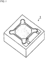
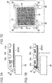
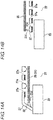
- Fig. 1 is a perspective view illustrating an example of a conventional acoustic sensor 1 manufactured by the MEMS technique.
- Fig. 2 is an exploded perspective view illustrating an example of an internal structure of the acoustic sensor 1.
- the acoustic sensor 1 is a laminated body formed by laminating an insulating film 4, a vibration electrode film (diaphragm) 5, and a back plate 7 on the top surface of a silicon substrate (hereinafter also referred to simply as a substrate) 3 provided with a back chamber 2.
- the back plate 7 has a structure where a fixed electrode film 8 is formed on a fixed plate 6, and is formed by disposing the fixed electrode film 8 on the fixed plate 6 on the silicon substrate 3 side.
- Sound holes are provided all over the fixed plate 6 of the back plate 7 as a large number of punched holes (each of meshed points on the fixed plate 6 illustrated in Fig. 2 corresponds to each of the sound holes). Further, a fixed electrode pad 10 for acquiring an output signal is provided at one of four corners of the fixed electrode film 8.
- the silicon substrate 3 can be formed by a single crystal silicon, for example.
- the vibration electrode film 5 can be formed by conductive polycrystal silicon, for example.
- the vibration electrode film 5 is a substantially rectangular thin film, in which fixed parts 12 are provided at four corners of a vibration part 11, having a substantially quadrilateral shape, that vibrates.
- the vibration electrode film 5 is disposed on the top surface of the silicon substrate 3 so as to cover the back chamber 2, and is fixed to the silicon substrate 3 at the four fixed parts 12 as anchor parts.
- the vibration part 11 of the vibration electrode film 5 reacts sensitively to sound pressure to vibrate vertically.
- the vibration electrode film 5 is not in contact with the silicon substrate 3 or the back plate 7 in a place other than the four fixed parts 12. This allows smoother vertical vibration of the vibration electrode film 5 after sensitive reaction to sound pressure. Further, a vibrating membrane electrode pad 9 is provided in one of the fixed parts 12 at the four corners of the vibration part 11.
- the fixed electrode film 8 provided in the back plate 7 is provided so as to correspond to the vibrating portion of the vibration electrode film 5 except for the fixed parts 12 at the four corners. This is because the fixed parts 12 at the four corners of the vibration electrode film 5 do not react sensitively to sound pressure to vibrate and hence capacitance between the vibration electrode film 5 and the fixed electrode film 8 remains unchanged.
- the sound passes through the sound hole to apply sound pressure to the vibration electrode film 5. That is, sound pressure is applied to the vibration electrode film 5 through this sound hole. Further, providing the sound hole can facilitate air in an air gap between the back plate 7 and the vibration electrode film 5 to escape to the outside, to reduce thermal noise, leading to noise reduction.
- the vibration electrode film 5 vibrates upon receipt of sound, and the distance between the vibration electrode film 5 and the fixed electrode film 8 changes.
- capacitance between the vibration electrode film 5 and the fixed electrode film 8 changes.
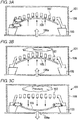
- FIGs. 3A to 3C are schematic views describing the case of excessive pressure acting on the acoustic sensor 1.
- the pressure acts on a vibration electrode film 105 from a pressure hole 106a provided at the bottom surface of a package 106 as the casing.
- the vibration electrode film 105 is greatly transformed to the back plate 107 side (opposite the pressure hole 106a), and the vibration electrode film 105 comes into contact with the back plate 107.
- the vibration electrode film 105 may be damaged at that time.
- the air having flown in from the pressure hole 106a in the above process passes through the gap between the vibration electrode film 105 and the back plate 107, further passes through a sound hole 107a of the back plate 107, and gets more deeply into the casing, to be compressed. Since this increases the pressure in the package 106, when the inflow of the air is ended, the increase in the pressure in the package 106 may then cause large transformation of the vibration electrode film 105 to the side opposite the back plate 107 (to the pressure hole 106a side), causing damage on the vibration electrode film 105. Such disadvantage can occur, for example, in a case where the acoustic sensor 1 falls or some other case in addition to the case where excessive air pressure acts on the acoustic sensor 1.
- Figs. 4A and 4B are considered. That is, as illustrated in Fig. 4A , by eliminating the sound hole 107a in a portion in the back plate 107, the portion facing the vicinity of the end of the vibration electrode film 105, it is possible to make it difficult for the air to pass through the back plate 107 via the sound hole 107a when excessive pressure acts from the pressure hole 106a.
- a projection is provided in the back plate, the projection cylindrically projecting to the vibration electrode film side so as to enclose the sound hole.
- the vibration electrode film is configured such that, when the vibration electrode film is transformed to the back plate side, the vibration electrode film abuts with the tip of the projection to block the sound hole and prevent passage of the air through the sound hole and through the back plate, and thereby prevent an increase in the pressure in the package.
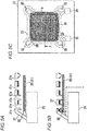
- Figs. 5A to 5C are views for describing a structure of the vicinity of a back plate 27 and a vibration electrode film 25 in the first embodiment.
- Fig. 5A is a sectional view illustrating a state before excessive pressure acts
- Fig. 5B is a sectional view illustrating a state where the excessive pressure has acted
- Fig. 5C is a plan view. Note that Figs. 5A and 5B are sectional views along an X-X cross section indicated in Fig. 5C .
- Fig. 5A and 5B are sectional views along an X-X cross section indicated in Fig. 5C .
- numeral 23 denotes a substrate
- numeral 29 denotes a vibrating membrane electrode pad
- numeral 30 denotes a fixed electrode pad
- numeral 31 denotes a vibration part in the vibration electrode film 25
- numeral 32 denotes a fixed part in the vibration electrode film 25.
- a projection 27c having a cylindrical shape is provided in the back plate 27 so as to enclose a sound hole 27a close to the end of the vibration electrode film 25 among sound holes 27a in the back plate 27.
- the vibration electrode film 25 abuts with the projection 27c to block the sound hole 27a, and can thus prevent the air from passing through the sound hole 27a to suppress the increase in the internal pressure of the package in terms of a region close to the end of the vibration electrode film 25.
- the presence of the projection 27c makes it difficult for the air to get into the gap between the back plate 27 and the vibration electrode film 25, and to reach the sound hole 27a disposed in a region close to the center of the vibration electrode film 25. It is thereby possible to prevent the air from passing through the sound hole 27a in the region to suppress the increase in the internal pressure of the package.
- the projection 27c may be provided at the sound hole 27a in a region A enclosing the vibration part 31 of the vibration electrode film 25, indicated by a dotted line in Fig. 5C , or may be provided at the sound hole 17a in a region extended in the center of the vibration part 31.
- the projection 27c may also be provided at the sound holes 27a in the whole region of the vibration part 31. Further, among the sound holes 27a in the above region, the projection 27c may be provided at each of all the sound holes 27a, or may be provided at each of some of the sound holes 27a.
- the size of the region provided with the projection 27c and the number of sound holes 27a provided with the projection 27c may be appropriately decided based on the degree of increase in the pressure in the package, the degree of occurrence of sticking, and the like, when excessive pressure acts on the acoustic sensor 1.
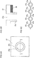
- Figs. 6A to 6C illustrate enlarged views of the sound hole 27a and the projection 27c.
- Fig. 6A is a plan view
- Fig. 6B is a Y-Y sectional view.
- the projection 27c is provided so as to enclose the sound hole 27a in a plan view, and has a cylindrical shape when the sound hole 27a has a circular shape.
- wall-shaped walls 27e link the projections 27c having a cylindrical shape as illustrated in the plan view of Fig. 6C . It is thereby possible to more reliably prevent the air from passing through the gap between the back plate 27 and the vibration electrode film 25 and through the sound hole 27a to suppress the increase in the pressure in the package.
- the projection 27c and the wall 27e correspond to the flow path cutoff part and the flow path inhibition part in the present invention.
- Figs. 7A to 7C are views for describing a structure of the vicinity of the back plate 27 and the vibration electrode film 25 in the second embodiment.
- Fig. 7A is a sectional view illustrating a state before excessive pressure acts
- Fig. 7B is a sectional view illustrating a state where the excessive pressure has acted
- Fig. 7C is a plan view. Note that Figs. 7A and 7B are sectional views along an X-X cross section indicated in Fig. 7C .
- a wall 27d is provided so as to surround a region, which is a portion facing the vibration part 31 of the vibration electrode film 25 and in which the sound holes 27a are distributed, in the back plate 27.
- the vibration part 31 of the vibration electrode film 25 abuts with the tip of the wall 27d to cut off a flow path for the air (inhibit the flow of the air) toward the region where the sound holes 27a are distributed in the back plate 27. It is thereby possible to prevent the air from passing through the sound hole 27a to suppress the increase in the pressure in the package.
- the wall 27d may be provided so as to surround a region B including all the sound holes 27a in Fig. 7C , or some of the sound holes 27a may be distributed outside the region surrounded by the wall 27d.
- the wall 27d may be provided so as to surround the whole of the vibration electrode film 25 including the fixed portion 32, as illustrated in Fig. 8C .
- Figs. 9A to 9C are views for describing a structure of the vicinity of the back plate 27 and the vibration electrode film 25 in a third embodiment.
- Fig. 9A is a sectional view illustrating a state before excessive pressure acts
- Fig. 9B is a sectional view illustrating a state where the excessive pressure has acted
- Fig. 9C is a plan view. Note that Figs. 9A and 9B are sectional views along an X-X cross section indicated in Fig. 9C .
- Fig. 9A and 9B are sectional views along an X-X cross section indicated in Fig. 9C .
- a projection 25a is provided in a position where each of the sound holes 27a disposed in the facing back plate 27 can be blocked in the vicinity of the end of the vibration part 31 of the vibration electrode film 25. That is, in a plan view, there has been provided the projection 25a having such a cross section in a columnar shape as to include each of the sound holes 27a.
- the projection 25a provided in the vibration electrode film 25 can block particularly the sound hole 27a disposed in a portion facing the vicinity of the end of the vibration part 31 of the vibration electrode film 25, which tends to be a flow path for the air. It is thereby possible to block the sound hole 27a disposed in the portion facing the vicinity of the end of the vibration part 31 of the vibration electrode film 25, and also possible to cut off a flow path for the air (inhibit the flow of the air) flowing into the gap between the vibration electrode film 25 and back plate 27 on the center side of the vibration electrode film 25. It is thereby possible to more efficiently prevent the air from passing through the sound hole 27a to suppress the increase in the pressure in the package.
- the projection 25a may be provided at the sound hole 27a in a region A enclosing the vibration part 31 of the vibration electrode film 25, indicated by a dotted line in Fig. 9C , or may be provided at the sound hole 27a in a region extended in the center of the vibration part 31.
- the projection 25a may be provided at each of the sound holes 27a facing the whole region of the vibration part 31 (i.e., at each of all the sound holes 27a disposed in the back plate 27). Further, among the sound holes 27a in the above region, the projection 25a may be provided at each of all the sound holes 27a, or may be provided at each of some of the extracted sound holes 27a.
- the size of the region provided with the projection 25a and the number of sound holes 27a provided with the projection 25a may be appropriately decided based on the degree of increase in the pressure in the package, the degree of occurrence of sticking, and the like, when excessive pressure acts on the acoustic sensor 1.
- the projection 25a having a columnar shape is provided in the vibration electrode film 25, the projection 25a being able to block each of the sound holes 27a in the facing back plate 27.
- the projection 25a may have a columnar shape being able to block a plurality of sound holes 27a.
- a wall is provided so as to surround at least a part of the vibration part 31 of the vibration electrode film 25, and when excessive pressure acts and the vibration electrode film 25 is transformed to the back plate 27 side, the sound hole 27a facing the region surrounded by this wall may be blocked.
- a structure where a hole 25b is provided in the vibration electrode film 25 Such a structure may be employed for the purpose of decreasing the sensitivity of a low-frequency region of the acoustic sensor 1.
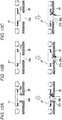
- Figs. 10A to 10C illustrate a structure of a projection 25c in the structure where the hole 25b is provided in the vibration electrode film 25.
- the projection 25c having a cylindrical shape may be provided in the vibration electrode film 25 so as to enclose the hole 25b.
- the projection 25c of the vibration electrode film 25 abuts with the back plate 27 to cut off a flow path for the air (inhibit the flow of the air) by the hole 25b in the vibration electrode film 25, so as to make it possible to prevent the air from passing through the hole 25b to suppress the increase in the pressure in the package.
- a projection 27e may be provided in the back plate 27, the projection 27e having a cross section that includes the hole 25b in a plan view. Accordingly, when excessive pressure acts and the vibration electrode film 25 is transformed to the back plate 27 side, the projection 27e of the back plate 27 abuts with the vibration electrode film 25 to cut off a flow path for the air (inhibit the flow of the air) by the hole 25b in the vibration electrode film 25, so as to make it possible to prevent the air from passing through the hole 25b to suppress the increase in the pressure in the package.
- a projection 27f may be provided in the back plate 27, the projection 27f having a cross section slightly smaller than the hole 25b in a plan view. Accordingly, when excessive pressure acts and the vibration electrode film 25 is transformed to the back plate 27 side, the projection 27f of the back plate 27 gets into the hole 25b in the vibration electrode film 25 to cut off a flow path for the air (inhibit the flow of the air), so as to make it possible to prevent the air from passing through the hole 25b to suppress the increase in the pressure in the package. Further, in this case, the risk of occurrence of sticking can be reduced by the projection abutting with the vibration electrode film 25.
- the flow path for the air passing through the hole 25b in the vibration electrode film 25 is cut off (the flow of the air is inhibited) directly. In the meantime, this indirectly cuts off at least a part of a flow path for a fluid passing through the gap between the vibration electrode film 25 and the back plate 27 and/or a flow path for a fluid passing through the sound hole of the back plate 27.
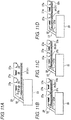
- the fixed electrode film is not provided in a portion in contact with the vibration electrode film, such as the tips of the projection and the wall provided on the back plate side (see Fig. 11A ). Accordingly, for example, even when the wall 27d illustrated in Fig. 11A comes into contact with the vibration electrode film 25 at the time of excessive pressure acting on the acoustic sensor 1, it is possible to prevent occurrence of an electrical short circuit between the vibration electrode film 25 and the back plate 27.
- Figs. 11B to 11D illustrate the relation of height between the wall 27d provided in the back plate 27 and a stopper 27b.
- the wall 27d is higher than the stopper 27b.
- the wall 27d is as high as the stopper 27b.
- the wall 27d it is preferable to make the wall 27d higher than the stopper 27b as illustrated in Fig. 11B , or make the wall 27d as high as the stopper 27b as illustrated in Fig. 11C . This also applies to the case where the projection is provided in the back plate 27.
- the air having flown in from the pressure hole 108b in the above process passes through the gap between the vibration electrode film 105 and the substrate 103, further passes through the opening of the substrate 103, and gets more deeply into the casing, to be compressed. Since the pressure in the package 108 thereby increases, when the inflow of the air is ended, the vibration electrode film 105 is greatly transformed to the back plate 107 side this time, to come into contact with the back plate 107. The vibration electrode film 105 may be damaged at that time.
- the wall is provided in the vibration electrode film on the substrate side, so as to make it difficult for the air to pass through an opening of the back chamber in the substrate to increase the pressure in the package.
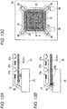
- Figs. 13A to 13C are views for describing a structure of the vicinity of the back plate 27 and the vibration electrode film 25 in the fifth embodiment.
- Fig. 13A is a sectional view illustrating a state before excessive pressure acts
- Fig. 13B is a sectional view illustrating a state where the excessive pressure has acted
- Fig. 13C is a plan view. Note that Figs. 13A and 13B are sectional views along an X-X cross section indicated in Fig. 13C .
- a wall 25d is provided in a portion, which faces a substrate 23, in the vibration electrode film 25 so as to surround a back chamber 22.
- the wall 25d of the vibration electrode film 25 abuts with the top surface of the substrate 23 to cut off a flow path for the air (inhibit the flow of the air) toward the back chamber 22, thereby enabling prevention of an increase in the pressure in the package.
- the wall 25d is provided so as to surround the opening of the back chamber 22 that is substantially square in a plan view, as indicated by a chain double-dashed line in Fig. 13C .
- the wall 25d is formed in a closed curve in a plan view in this case, the wall 25d may have a gap in a part thereof.
- a stopper (not illustrated) may be provided on the surface of the vibration electrode film 25 on the substrate 23 side in order to prevent occurrence of sticking between the vibration electrode film 25 and the substrate 23.
- a vibration electrode film 35 is disposed in a back plate 37 on the ceiling surface side (i.e., on the pressure hole side) as illustrated in Figs. 13A to 13C and Fig. 14A
- a wall 37d may be provided so as to surround a region where a sound hole 37a is disposed in the back plate 37.
- a cylindrical projection may be provided in the back plate 37 so as to surround the sound hole 37a. Further, such a projection as to block the sound hole 37a may be provided in the vibration electrode film 35.
- the projection or the wall may be formed by adding a curved shape to the back plate or the vibration electrode film.
- FIG. 15A and 15B illustrates a sectional view of the vicinity of the back plate and the vibration electrode film in such a modified example.
- Fig. 15A is an example where a curved shape is added to the obliquely formed side surface of the back plate 27 to form a wall 27f.
- the end surface of the vibration part 31 comes close to the wall 27f, to cut off a flow path (inhibit the flow) at the time of the air flowing into the gap between the back plate 27 and the vibration electrode film 25 and prevent passage of the air through the sound hole 27a. It is thereby possible to prevent an increase in the pressure in the package.
- the end surface of the vibration part 31 comes close to the wall 27f, to cut off a flow path (inhibit the flow) at the time of the air flowing into the gap between the back plate 27 and the vibration electrode film 25.
- the surface of the vibration electrode film 25 on the back plate 27 side may abut with the wall 27f, to cut off the flow path (inhibit the flow) at the time of the air flowing into the gap between the back plate 27 and the vibration electrode film 25.
- Fig. 15B is an example where a projection 25e of the vibration electrode film 25 is formed by adding a curved shape to a part of the end of the vibration part 31 in the vibration electrode film 25. Also in this example, when excessive pressure acts on the acoustic sensor 1 and the vibration electrode film 25 is transformed to the back plate 27 side, the projection 25e blocks the sound hole 27a of the back plate 27, to cut off a flow path (inhibit the flow) at the time of the air flowing into the gap between the back plate 27 and the vibration electrode film 25 and prevent passage of the air through the sound hole 27a. It is thereby possible to prevent an increase in the pressure in the package.
- the example has been described where excessive pressure acts on the acoustic sensor 1 and the air flows in from the pressure hole.
- the present invention is also applicable to a case where the acoustic sensor 1 is used in an atmosphere other than the air. That is, the flow path cutoff part and the flow path inhibition part in the present invention may cut off a flow path for a fluid other than the air or inhibit the flow of the fluid.
- the vibration part of the vibration electrode film has been in a substantially square shape and the fixed parts have been formed on its periphery.
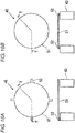
- the vibration part of the vibration electrode film may be in a circular shape as illustrated in Figs 16A and 16B or other shapes.
- one or more fixed parts 52 may be provided on the periphery of the circular vibration part 51 in a vibration electrode film 45 so as to radially extend as illustrated in Fig. 16A , or an outer peripheral portion of the circular vibration part 51 in the vibration electrode film 45 may directly function as the fixed part 52 that is fixed to the substrate 43 (or a back plate, not illustrated) as illustrated in Fig. 16B .
Abstract


Description
- This application is based on Japanese Patent Application No.
2016-240655 - The present invention relates to an acoustic sensor where a capacitive transducer is housed in a casing, and the capacitive transducer in the acoustic sensor. More specifically, the present invention relates to an acoustic sensor where a capacitive transducer is housed in a casing, the capacitive transducer being configured in a capacitor structure formed by the MEMS technique and including a vibration electrode film and a back plate. Further, the present invention relates to the capacitive transducer.
- There have been cases where a product using an acoustic sensor, called an ECM (Electret Condenser Microphone), is used as a small-sized microphone. However, the ECM is easily affected by heat, and in terms of digitization support and size reduction, a microphone using a capacitive transducer is more excellent, the capacitive transducer being manufactured by using the MEMS (Micro Electro Mechanical Systems) technique (hereinafter this microphone is also referred to as an MEMS microphone). Thus, in the recent years, the MEMS microphone is being employed (e.g., see Japanese Unexamined Patent Publication No.
2011-250170 - Some of the acoustic sensors as described above house a capacitive transducer having achieved a figuration by using the MEMS technique, the figuration being where a vibration electrode film that vibrates under pressure is disposed facing a back plate fixed with the electrode film via a void. The figuration of the capacitive transducer as thus described can be achieved, for example, by the following step: forming on a silicon substrate a vibration electrode film and such a sacrifice layer as to cover the vibration electrode; forming a back plate on the sacrifice layer; and removing the sacrifice layer. With the semiconductor manufacturing technique applied to the MEMS technique as above, it is possible to obtain an extremely small capacitive transducer.
- Meanwhile, since the capacitive transducer prepared by using the MEMS technique is made up of the vibration electrode film and the back plate having been reduced in thickness, the vibration electrode film is liable to be greatly transformed and damaged when excessive pressure acts thereon, or in some other case. Such disadvantage may occur, for example, in a case where large sound pressure is applied into a casing (package) having a pressure hole while the capacitive transducer is housed in the casing. It may also occur in a case where air is blown to the pressure hole of the casing in a package process, or in a case where the capacitive transducer in the state of being housed in the casing falls. This also applies to a case where large sound pressure is applied or air is blown to a mobile electronic device such as a smart phone which includes the capacitive transducer in the state of being housed in the casing, or a case where the device is dropped.
- More specifically, when compressed air flows in from the pressure hole that brings air into the capacitive transducer due to collision by falling or the use of an air gun, the vibration electrode film is greatly transformed to the back plate side (opposite the pressure hole) or the substrate side (at this point, the vibration electrode film may be damaged by coming into contact with the back plate or the substrate). The air having entered the capacitive transducer from the pressure hole passes through a gap between the vibration electrode film and the semiconductor substrate or the back plate and/or an opening of the semiconductor substrate or a sound hole of the back plate and gets more deeply into the casing, while transforming the vibration electrode film, to increase the pressure in the casing. When the inflow of the compressed air is ended due to the increased pressure in the casing, the pressure in the casing may cause excessive transformation of the vibration electrode film to the pressure hole side and damage on the vibration electrode film.
- In contrast, there is known a technique of mechanically suppressing displacement of a diaphragm to prevent damage due to excessive transformation of the diaphragm (e.g., see
US Patent No. 2008/0031476 ). However, in this technique, the transformation of the diaphragm can be suppressed, but an increase in the pressure itself cannot be prevented. There has thus been a risk that stress concentrates on a part of the diaphragm due to contact between the diaphragm and a transformation suppressing member to cause damage on the diaphragm. - There is also known a technique of disposing a support structure on the substrate side in a diaphragm to prevent collision of the diaphragm with a substrate due to excessive pressure, and damage on the diaphragm (e.g., see
US Patent No. 2015/0256924 ). However, in this technique, the placement of the support structure may complicate the structure to cause deterioration in productivity and an increase in manufacturing cost. Further, Brownian motion of the air present between the diaphragm and the support structure below the diaphragm may cause noise. - The present invention has been made in view of such circumstances as above, and is to particularly prevent internal pressure of a casing that houses a capacitive transducers from increasing due to compressed air flown in from a pressure hole of an acoustic sensor, and to prevent a vibration electrode film from being damaged by being excessively transformed to the pressure hole side caused by the pressure. That is, an object of the present invention is to provide a technique by which, when excessive pressure acts on an acoustic sensor, an increase in pressure in a casing is prevented to suppress excessive transformation of a vibration electrode film of a capacitive transducer caused by the increased pressure.
- One aspect of present invention for solving the above problem is an acoustic sensor including: a semiconductor substrate having an opening; a back plate disposed so as to face the opening of the semiconductor substrate, configured to function as a fixed electrode, and having sound holes that allow passage of air; a vibration electrode film disposed so as to face the back plate through a void; and a casing configured to house the substrate, the back plate, and the vibration electrode film, and having a pressure hole that allows inflow of air, the acoustic sensor converting transformation of the vibration electrode film into a change in capacitance between the vibration electrode film and the back plate to detect sound pressure. In the acoustic sensor, a flow path is formed, which includes any of the sound hole of the back plate, a gap between the back plate and the vibration electrode film, a gap between the vibration electrode film and the semiconductor substrate, and the opening of the semiconductor substrate, and in which a fluid having flown into the casing from the pressure hole moves to a space opposite the pressure hole in the casing across the vibration electrode film, and a flow path cutoff part is further provided, being configured to cut off at least a part of the flow path when the vibration electrode film is transformed to come close to the semiconductor substrate or the back plate due to the fluid flowing into the casing from the pressure hole.
- When excessive pressure acts on the acoustic sensor, the air having entered the casing of the acoustic sensor from the pressure hole passes through the gap between the vibration electrode film and the semiconductor substrate or the back plate and/or the opening of the semiconductor substrate or the sound hole of the back plate and gets more deeply into the casing, while transforming the vibration electrode film of the capacitive transducer housed in the casing, to increase the pressure, especially in a region opposite the pressure hole across the vibration electrode film in the casing. Then, the vibration electrode film is excessively transformed to the pressure hole side caused by the increased pressure in the casing. In contrast, in the present invention, a flow path is formed, which includes any of the sound hole of the back plate, the gap between the back plate and the vibration electrode film, the gap between the vibration electrode film and the semiconductor substrate, and the opening of the semiconductor substrate, and in which a fluid having flown in from the pressure hole to the casing moves to a space opposite the pressure hole across the vibration electrode film in the casing, and a flow path cutoff part is further provided, being configured to cut off at least a part of the flow path when the vibration electrode film is transformed to come close to the semiconductor substrate or the back plate due to the fluid flowing into the casing from the pressure hole. That is, according to the present invention, when excessive pressure acts on the acoustic sensor, it is possible to prevent passage of the air through the gap between the vibration electrode film and the semiconductor substrate or the back plate of the capacitive transducer housed in the casing and/or the opening of the semiconductor substrate or the sound hole of the back plate to suppress the increase in the pressure especially in a region opposite the pressure hole across the vibration electrode film in the casing, and to suppress excessive transformation of the vibration electrode film caused by the pressure. It is thereby possible to prevent damage on the vibration electrode film when excessive pressure acts on the acoustic sensor. Note that the meaning of cutting off includes the case of leaving a part of passage of the fluid, in addition to the case of completely blocking passage of the fluid.
- Further, in the present invention, the flow path cutoff part may be a projection provided in one of the vibration electrode film and the back plate, and configured to block each of at least some of the sound holes in the back plate by abutting with the other of the vibration electrode film and the back plate when the vibration electrode film is transformed to come close to the back plate.
- In the configuration where the pressure hole in the casing is positioned opposite the back place across the vibration electrode film, when excessive pressure acts on the acoustic sensor, the vibration electrode film in the capacitive transducer is greatly transformed not to the semiconductor substrate side, but to the back plate side. In such a case, the air passes through the gap between the vibration electrode film and the back plate and/or the sound hole of the back plate and gets more deeply into the casing to increase the pressure in the casing. In contrast, in the present invention, when the vibration electrode film transforms and comes close to the back plate, the projection provided in the back plate abuts with the vibration electrode film to block each of at least some of the sound holes in the back plate.
- According to this, when excessive pressure acts on the acoustic sensor, it is possible to prevent the air having entered from the pressure hole of the casing from passing through the sound hole of the back plate in the capacitive transducer and getting more deeply into the casing to suppress the increase in the pressure in the casing. It is thereby possible to prevent excessive transformation of the vibration electrode film to the pressure hole side caused by the increased pressure, and to avoid damage on the vibration electrode film.
- Further, in the present invention, the projection may block each of the sound holes all over the back plate. According to this, when excessive pressure acts on the acoustic sensor, it is possible to more reliably prevent the air from passing through the sound hole of the back plate in the capacitive transducer and getting more deeply into the casing to suppress the increase in the pressure in the casing.
- Further, in the present invention, the vibration electrode film may be formed including a platy vibration part on which pressure acts, and a fixed part configured to fix the vibration part to the semiconductor substrate, and the projection may block the sound hole disposed in a portion in the back plate, the portion facing an outer periphery of the vibration part of the vibration electrode film. When excessive pressure acts on the acoustic sensor and the vibration electrode film in the capacitive transducer is greatly transformed to the back plate side, the air having entered from the pressure hole first gets into the gap between the vibration electrode film and the back plate from the outer periphery of the vibration part of the vibration electrode film. Thereafter, the air passes the sound hole of the back plate and gets more deeply into the casing to increase the pressure in the casing. Therefore, by causing the projection to block the sound hole disposed in the portion in the back plate, the portion facing the outer periphery of the vibration part of the vibration electrode film, it is possible to prevent passage of the air through the sound hole disposed in the vicinity of the outer periphery of the vibration part of the vibration electrode film, and to prevent the flow of the air toward the center of the gap between the vibration electrode film and the back plate. It is thereby possible to more efficiently prevent passage of the air through the sound holes all over the back plate, and more efficiently prevent an increase in the pressure in the casing, and damage on the vibration electrode film caused by the pressure.
- Further, in the present invention, the projection may have a cylindrical shape enclosing the sound hole in the back plate in a plan view. According to this, when the vibration electrode film is transformed to come close to the back plate, each of the sound holes in the back plate are surrounded by each of the cylindrical projections and the vibration electrode film, thus making it possible to more reliably block the sound holes. As a result, when excessive pressure acts on the acoustic sensor, it is possible to more reliably prevent the air from passing through the sound hole of the back plate and getting more deeply into the casing to suppress the increase in the pressure in the casing.
- Further, in the present invention, the vibration electrode film may be formed including a platy vibration part on which pressure acts, and a fixed part configured to fix the vibration part to the semiconductor substrate or the back plate, and the flow path cutoff part may be a wall provided in one of the vibration electrode film and the back plate, and formed so as to surround at least a part of the vibration part in the vibration electrode film or surround at least a portion in the back plate, the portion facing a part of the vibration part of the vibration electrode film, and when the vibration electrode film is transformed to come close to the back plate, the flow path cutoff part abuts with the other of the vibration electrode film and the back plate to block up at least a part of a flow path for air that passes through the gap between the vibration electrode film and the back plate and/or the sound hole of the back plate.
- In this case, when the vibration electrode film comes close to the back plate, the projection does not block each of the sound holes in the back plate, but the wall formed so as to surround at least a portion in the back plate, in which the portion faces a part of the vibration part of the vibration electrode film, blocks all or at least some of the sound holes in the back plate. It is thus possible to more efficiently cut off the flow path for the air (inhibit the flow of the air) passing through the sound hole of the back plate. At the same time, it is possible to more efficiently cut off the flow path for the air passing through the gap between the vibration electrode film and the back plate.
- Further, in the present invention, the back plate may be provided with a fixed electrode film and the flow path cutoff part, and the fixed electrode film may be provided only in a portion other than a tip of the flow path cutoff part in the back plate. That is, not forming the fixed electrode film at the tip of the flow path cutoff part (e.g., the projection or the wall described above) can prevent occurrence of an electrical short circuit when the flow path cutoff part abuts with the back plate, the semiconductor substrate, the vibration electrode film, or the like.
- Further, in the present invention, a stopper may further be provided in one of the fixed electrode film and the back plate, the stopper being configured to abut with the other of the fixed electrode film and the back plate when the fixed electrode film and the stopper come close to each other, and the flow path cutoff part may be set as high as or higher than the stopper.
- According to this, the flow path cutoff part provided in the vibration electrode film or the back plate can be made higher than the stopper configured to prevent sticking between the vibration electrode film and the back plate when those come close to each other. It is thereby possible to avoid the stopper preventing the flow path cutoff part from abutting with the vibration electrode film or the back plate. Therefore, when excessive pressure acts on the acoustic sensor, it is possible to more reliably prevent an increase in the pressure in the casing and to suppress excessive transformation of the vibration electrode film caused by the above pressure, and to prevent damage on the vibration electrode film at that time.
- Further, in the present invention, the vibration electrode film may be formed including a platy vibration part on which pressure acts, and a fixed part configured to fix the vibration part to the semiconductor substrate or the back plate, and the flow path cutoff part may be a wall provided in one of the vibration electrode film and the semiconductor substrate, and formed so as to surround at least the opening in the semiconductor substrate, or surround at least a portion in the vibration electrode film, the portion facing the opening of the semiconductor substrate, and abuts with the other of the vibration electrode film and the semiconductor substrate to cut off at least a part of a flow path for air that passes through the gap between the vibration electrode film and the semiconductor substrate and/or the opening of the semiconductor substrate when the vibration electrode film is transformed to come close to the semiconductor substrate.
- Here, a configuration is assumed where the vibration electrode film is transformed to the semiconductor substrate side opposite the back plate when pressure acts on the acoustic sensor. In this case, the wall as the flow path cutoff part is provided in one of the vibration electrode film and the semiconductor substrate, and formed so as to surround at least the opening in the semiconductor substrate or to surround at least a portion in the vibration electrode film, the portion facing the opening of the semiconductor substrate. Thus, when the vibration electrode film is transformed to come close to the semiconductor substrate, the wall abuts with the other of the vibration electrode film and the semiconductor substrate to cut off the flow path for the air (inhibit the flow of the air) passing through the gap between the vibration electrode film and the semiconductor substrate and/or the opening of the semiconductor substrate. As a result, when excessive pressure acts on the capacitive transducer, it is possible to more reliably prevent the air from passing through the opening of the semiconductor substrate to suppress the increase in the pressure in the casing, and avoid the vibration electrode film being excessively transformed and damaged due to the pressure. Also in this case, the stopper is further provided in one of the vibration electrode film and the semiconductor substrate, the stopper being configured to abut with the other of the vibration electrode film and the semiconductor substrate when the vibration electrode film and the semiconductor substrate come close to each other, and the wall is made as high as or higher than the stopper. It is thereby possible to avoid the stopper preventing the flow path cutoff part from abutting with the vibration electrode film or the back plate.
- Further, one aspect of the present invention is an acoustic sensor including: a semiconductor substrate having an opening; a back plate disposed so as to face the opening of the semiconductor substrate, and having sound holes that allow passage of air; a vibration electrode film disposed so as to face the back plate through a void; and a casing configured to house the substrate, the back plate, and the vibration electrode film, and having a pressure hole that allows inflow of air, the acoustic sensor converting transformation of the vibration electrode film into a change in capacitance between the vibration electrode film and the back plate to detect sound pressure. In the acoustic sensor, a flow path inhibition part may further be provided, being configured to inhibit a flow of a fluid that passes through the opening of the semiconductor substrate or the sound hole of the back plate when the vibration electrode film is transformed to come close to the semiconductor substrate or the back plate.
- Also according to this, when excessive pressure acts on the acoustic sensor, it is possible to prevent the air from passing through the opening of the semiconductor substrate or the sound hole of the back plate to increase the pressure in the casing, and to suppress excessive transformation of the vibration electrode film caused by the pressure. It is thereby possible to prevent damage on the vibration electrode film when excessive pressure acts on the acoustic sensor.
- Further, one aspect of the present invention is a capacitive transducer which is used by being housed in a casing having a pressure hole that allows inflow of air, the capacitive transducer including: a semiconductor substrate having an opening; a back plate disposed so as to face the opening of the semiconductor substrate, configured to function as a fixed electrode, and having sound holes that allow passage of air; and a vibration electrode film disposed so as to face the back plate through a void. In the capacitive transducer, transformation of the vibration electrode film may be converted into a change in capacitance between the vibration electrode film and the back plate, and a flow path cutoff part may further be provided, being configured to cut off at least a part of a flow path for a fluid that passes through a gap between the vibration electrode film and the semiconductor substrate or the back plate and/or a flow path for a fluid that passes through the opening of the semiconductor substrate or the sound hole of the back plate when the vibration electrode film is transformed to come close to the semiconductor substrate or the back plate.
- According to the capacitive transducer in the present invention, in a case where the capacitive transducer is housed in the casing and used as the acoustic sensor, when excessive pressure acts on the acoustic sensor, it is possible to prevent the air from passing through the gap between the vibration electrode film and the semiconductor substrate or the back plate of the capacitive transducer housed in the casing and/or the opening of the semiconductor substrate or the sound hole of the back plate to suppress the increase in the pressure especially in a region opposite the pressure hole across the vibration electrode film in the casing, and to suppress excessive transformation of the vibration electrode film caused by the pressure. It is thereby possible to prevent damage on the vibration electrode film of the capacitive transducer when excessive pressure acts on the acoustic sensor.
- Further, in that case, the flow path cutoff part may be a projection provided in one of the vibration electrode film and the back plate, and configured to block each of at least some of the sound holes in the back plate by abutting with the other of the vibration electrode film and the back plate when the vibration electrode film is transformed to come close to the back plate.
- Further, in the capacitive transducer according to the present invention, the projection may block each of the sound holes all over the back plate.
- Further, in the capacitive transducer according to the present invention, the vibration electrode film may be formed including a platy vibration part on which pressure acts, and a fixed part configured to fix the vibration part to the semiconductor substrate or the back plate, and the projection may block the sound hole disposed in a portion in the back plate, the portion facing an outer periphery of the vibration part of the vibration electrode film.
- Further, in the capacitive transducer according to the present invention, the projection has a cylindrical shape enclosing the sound hole in the back plate in a plan view.
- Further, in the capacitive transducer according to the present invention, the vibration electrode film may be formed including a platy vibration part on which pressure acts, and a fixed part configured to fix the vibration part to the semiconductor substrate or the back plate, and the flow path cutoff part may be a wall provided in one of the vibration electrode film and the back plate, and formed so as to surround at least a part of the vibration part in the vibration electrode film or to surround at least a portion in the back plate, the portion facing a part of the vibration part of the vibration electrode film, and abuts with the other of the vibration electrode film and the back plate to cut off at least a part of a flow path for air that passes through the gap between the vibration electrode film and the back plate and/or the sound hole of the back plate when the vibration electrode film is transformed to come close to the back plate.
- Further, in the capacitive transducer according to the present invention, the back plate may be provided with a fixed electrode film and the flow path cutoff part, and the fixed electrode film may be provided only in a portion other than a tip of the flow path cutoff part in the back plate.
- Further, in the capacitive transducer according to the present invention, a stopper may further be provided in one of the vibration electrode film and the back plate, the stopper being configured to abut with the other of the vibration electrode film and the back plate when the vibration electrode film and the back plate come close to each other, and the flow path cutoff part may be set as high as or higher than the stopper.
- Further, in the capacitive transducer according to the present invention, the vibration electrode film may be formed including a platy vibration part on which pressure acts, and a fixed part configured to fix the vibration part to the semiconductor substrate or the back plate, and the flow path cutoff part may be a wall provided in one of the vibration electrode film and the semiconductor substrate, and formed so as to surround at least the opening in the semiconductor substrate, or to surround at least a portion in the vibration electrode film, the portion facing the opening of the semiconductor substrate, and abuts with the other of the vibration electrode film and the semiconductor substrate to cut off at least a part of a flow path for air that passes through the gap between the vibration electrode film and the semiconductor substrate and/or the opening of the semiconductor substrate when the vibration electrode film is transformed to come close to the semiconductor substrate.
- Further, in the capacitive transducer according to the present invention, a stopper may further be provided in one of the vibration electrode film and the semiconductor substrate, the stopper being configured to abut with the other of the vibration electrode film and the semiconductor substrate when the vibration electrode film and the semiconductor substrate come close to each other, and the wall may be set as high as or higher than the stopper.
- Further, the capacitive transducer according to one aspect of the present invention is a capacitive transducer which is used by being housed in a casing having a pressure hole that allows inflow of air, the capacitive transducer including: a semiconductor substrate having an opening on a surface; a back plate disposed so as to face the opening of the semiconductor substrate, and having sound holes that allow passage of air; and a vibration electrode film disposed so as to face the back plate through a void. In the capacitive transducer, transformation of the vibration electrode film may be converted into a change in capacitance between the vibration electrode film and the back plate, and a flow path inhibition part may further be provided, being configured to inhibit a flow of a fluid that passes through the opening of the semiconductor substrate or the sound hole of the back plate when the vibration electrode film is transformed to come close to the semiconductor substrate or the back plate.
- Note that means for solving the problem described above can be used in appropriate combination.
- According to the present invention, it is possible to prevent an increase in pressure in a casing when excessive pressure acts on an acoustic sensor, and to suppress excessive transformation of a vibration electrode film of a capacitive transducer caused by the increased pressure. It is thereby possible to improve tolerance of the acoustic sensor when excessive pressure acts on the acoustic sensor.
-
-
Fig. 1 is a perspective view illustrating an example of a conventional acoustic sensor manufactured by the MEMS technique; -
Fig. 2 is an exploded perspective view illustrating an example of an internal structure of the conventional acoustic sensor; -
Figs. 3A to 3C are views for describing disadvantage in the case of excessive pressure abruptly acting on the acoustic sensor; -
Figs. 4A and 4B are views for describing a conventional measure against the case of excessive pressure abruptly acting on the acoustic sensor; -
Figs. 5A to 5C are views illustrating a configuration of the vicinity of the vibration electrode film and the back plate in a first embodiment of the present invention; -
Figs. 6A to 6C are views illustrating a configuration of a projection in the first embodiment of the present invention; -
Figs. 7A to 7C are views illustrating a configuration of the vicinity of the vibration electrode film and the back plate in a second embodiment of the present invention; -
Figs. 8A to 8C are views illustrating another configuration of the vicinity of the vibration electrode film and the back plate in the second embodiment of the present invention. -
Figs. 9A to 9C are views illustrating a configuration of the vicinity of the vibration electrode film and the back plate in a third embodiment of the present invention; -
Figs. 10A to 10C are views illustrating a configuration of the vicinity of the vibration electrode film and the back plate in a fourth embodiment of the present invention; -
Figs. 11A to 11D are views for describing states of tips of the projection/wall and the relation between the stopper and heights of the projection/wall in the embodiments of the present invention. -
Figs. 12A to 12C are second views for describing disadvantage in the case of excessive pressure abruptly acting on the acoustic sensor. -
Figs. 13A to 13C are views illustrating a configuration of the vicinity of the vibration electrode film and the back plate in a fifth embodiment of the present invention; -
Figs 14A and 14B are views illustrating a configuration of the vicinity of the vibration electrode film and the back plate in the case of provision of a pressure hole on the ceiling surface of the package. -
Figs. 15A and 15B are views illustrating a configuration of the vicinity of the vibration electrode film and the back plate in a modified example of the present invention; and -
Figs. 16A and 16B are views illustrating another example of the vibration electrode film of the present invention. - Hereinafter, a first embodiment of the present invention will be described with reference to the drawings. Each of the embodiments shown below is an aspect of the present invention, and is not intended to restrict the technical scope of the present invention. In the following, the case of using a capacitive transducer as an acoustic sensor will be described. However, the capacitive transducer according to the present invention is configured to detect displacement of a vibration electrode film, and can thus be used as a sensor other than the acoustic sensor. For example, it may be used as a pressure sensor, or may be used as an acceleration sensor, an inertia sensor, or some other sensor. It may also be used as an element other than the sensor, such as a speaker for converting an electrical signal into displacement. Further, the placement of a back plate, a vibration electrode film, a back chamber, a semiconductor substrate, and the like in the following description is an example. This placement is not restrictive so long as an equivalent function is exerted. For example, the placement of the back plate and the vibration electrode film may be reversed.
-
Fig. 1 is a perspective view illustrating an example of a conventional acoustic sensor 1 manufactured by the MEMS technique.Fig. 2 is an exploded perspective view illustrating an example of an internal structure of the acoustic sensor 1. The acoustic sensor 1 is a laminated body formed by laminating an insulating film 4, a vibration electrode film (diaphragm) 5, and aback plate 7 on the top surface of a silicon substrate (hereinafter also referred to simply as a substrate) 3 provided with aback chamber 2. Theback plate 7 has a structure where a fixed electrode film 8 is formed on afixed plate 6, and is formed by disposing the fixed electrode film 8 on the fixedplate 6 on the silicon substrate 3 side. Sound holes are provided all over the fixedplate 6 of theback plate 7 as a large number of punched holes (each of meshed points on the fixedplate 6 illustrated inFig. 2 corresponds to each of the sound holes). Further, a fixedelectrode pad 10 for acquiring an output signal is provided at one of four corners of the fixed electrode film 8. - The silicon substrate 3 can be formed by a single crystal silicon, for example. The
vibration electrode film 5 can be formed by conductive polycrystal silicon, for example. Thevibration electrode film 5 is a substantially rectangular thin film, in which fixedparts 12 are provided at four corners of avibration part 11, having a substantially quadrilateral shape, that vibrates. Thevibration electrode film 5 is disposed on the top surface of the silicon substrate 3 so as to cover theback chamber 2, and is fixed to the silicon substrate 3 at the four fixedparts 12 as anchor parts. Thevibration part 11 of thevibration electrode film 5 reacts sensitively to sound pressure to vibrate vertically. - The
vibration electrode film 5 is not in contact with the silicon substrate 3 or theback plate 7 in a place other than the four fixedparts 12. This allows smoother vertical vibration of thevibration electrode film 5 after sensitive reaction to sound pressure. Further, a vibratingmembrane electrode pad 9 is provided in one of the fixedparts 12 at the four corners of thevibration part 11. The fixed electrode film 8 provided in theback plate 7 is provided so as to correspond to the vibrating portion of thevibration electrode film 5 except for the fixedparts 12 at the four corners. This is because the fixedparts 12 at the four corners of thevibration electrode film 5 do not react sensitively to sound pressure to vibrate and hence capacitance between thevibration electrode film 5 and the fixed electrode film 8 remains unchanged. - When sound reaches the acoustic sensor 1, the sound passes through the sound hole to apply sound pressure to the
vibration electrode film 5. That is, sound pressure is applied to thevibration electrode film 5 through this sound hole. Further, providing the sound hole can facilitate air in an air gap between theback plate 7 and thevibration electrode film 5 to escape to the outside, to reduce thermal noise, leading to noise reduction. - In the acoustic sensor 1, with the structure described above, the
vibration electrode film 5 vibrates upon receipt of sound, and the distance between thevibration electrode film 5 and the fixed electrode film 8 changes. When the distance between thevibration electrode film 5 and the fixed electrode film 8 changes, capacitance between thevibration electrode film 5 and the fixed electrode film 8 changes. Hence it is possible to detect sound pressure as an electrical signal by previously applying a direct-current voltage between the vibratingmembrane electrode pad 9 electrically connected with thevibration electrode film 5 and the fixedelectrode pad 10 electrically connected with the fixed electrode film 8, and taking out the above-mentioned change in capacitance as an electrical signal. - Next, a description will be given of disadvantage that can occur in the above conventional acoustic sensor 1.
Figs. 3A to 3C are schematic views describing the case of excessive pressure acting on the acoustic sensor 1. As illustrated inFigs. 3A to 3C , when excessive pressure acts on the acoustic sensor 1, the pressure acts on avibration electrode film 105 from apressure hole 106a provided at the bottom surface of apackage 106 as the casing. Then, thevibration electrode film 105 is greatly transformed to theback plate 107 side (opposite thepressure hole 106a), and thevibration electrode film 105 comes into contact with theback plate 107. Thevibration electrode film 105 may be damaged at that time. - Further, the air having flown in from the
pressure hole 106a in the above process passes through the gap between thevibration electrode film 105 and theback plate 107, further passes through asound hole 107a of theback plate 107, and gets more deeply into the casing, to be compressed. Since this increases the pressure in thepackage 106, when the inflow of the air is ended, the increase in the pressure in thepackage 106 may then cause large transformation of thevibration electrode film 105 to the side opposite the back plate 107 (to thepressure hole 106a side), causing damage on thevibration electrode film 105. Such disadvantage can occur, for example, in a case where the acoustic sensor 1 falls or some other case in addition to the case where excessive air pressure acts on the acoustic sensor 1. - Especially against the disadvantage caused by the increase in the pressure in the
package 106, measures as illustrated inFigs. 4A and 4B are considered. That is, as illustrated inFig. 4A , by eliminating thesound hole 107a in a portion in theback plate 107, the portion facing the vicinity of the end of thevibration electrode film 105, it is possible to make it difficult for the air to pass through theback plate 107 via thesound hole 107a when excessive pressure acts from thepressure hole 106a. - However, in this case, since the air is accumulated between the
vibration electrode film 105 and theback plate 107 in the vicinity of the end of thevibration electrode film 105, noise tends to occur due to Brownian motion of the air, which is disadvantageous. Further, as illustrated inFig. 4B , by eliminating astopper 107b of theback plate 107, when thevibration electrode film 105 is transformed to theback plate 107 side, it is possible to bring the whole surfaces of thevibration electrode film 105 and theback plate 107 into intimate contact with each other and make it difficult for the air to pass through theback plate 107 via thesound hole 107a. However, in this case, thevibration electrode film 105 and theback plate 107 are liable to stay in intimate contact and become unable to be separated, thus causing occurrence of sticking. - Accordingly, in the first embodiment, for dealing with the above disadvantage, a projection is provided in the back plate, the projection cylindrically projecting to the vibration electrode film side so as to enclose the sound hole. Namely, it is configured such that, when the vibration electrode film is transformed to the back plate side, the vibration electrode film abuts with the tip of the projection to block the sound hole and prevent passage of the air through the sound hole and through the back plate, and thereby prevent an increase in the pressure in the package.
-
Figs. 5A to 5C are views for describing a structure of the vicinity of aback plate 27 and avibration electrode film 25 in the first embodiment.Fig. 5A is a sectional view illustrating a state before excessive pressure acts,Fig. 5B is a sectional view illustrating a state where the excessive pressure has acted, andFig. 5C is a plan view. Note thatFigs. 5A and 5B are sectional views along an X-X cross section indicated inFig. 5C . InFig. 5A , numeral 23 denotes a substrate, numeral 29 denotes a vibrating membrane electrode pad, numeral 30 denotes a fixed electrode pad, numeral 31 denotes a vibration part in thevibration electrode film 25, and numeral 32 denotes a fixed part in thevibration electrode film 25. As illustrated inFig. 5A , aprojection 27c having a cylindrical shape is provided in theback plate 27 so as to enclose asound hole 27a close to the end of thevibration electrode film 25 amongsound holes 27a in theback plate 27. - Accordingly, when excessive pressure acts and the
vibration electrode film 25 is transformed to theback plate 27 side, thevibration electrode film 25 abuts with theprojection 27c to block thesound hole 27a, and can thus prevent the air from passing through thesound hole 27a to suppress the increase in the internal pressure of the package in terms of a region close to the end of thevibration electrode film 25. Further, the presence of theprojection 27c makes it difficult for the air to get into the gap between theback plate 27 and thevibration electrode film 25, and to reach thesound hole 27a disposed in a region close to the center of thevibration electrode film 25. It is thereby possible to prevent the air from passing through thesound hole 27a in the region to suppress the increase in the internal pressure of the package. - Note that the
projection 27c may be provided at thesound hole 27a in a region A enclosing thevibration part 31 of thevibration electrode film 25, indicated by a dotted line inFig. 5C , or may be provided at the sound hole 17a in a region extended in the center of thevibration part 31. Theprojection 27c may also be provided at thesound holes 27a in the whole region of thevibration part 31. Further, among thesound holes 27a in the above region, theprojection 27c may be provided at each of all thesound holes 27a, or may be provided at each of some of thesound holes 27a. The size of the region provided with theprojection 27c and the number ofsound holes 27a provided with theprojection 27c may be appropriately decided based on the degree of increase in the pressure in the package, the degree of occurrence of sticking, and the like, when excessive pressure acts on the acoustic sensor 1. -
Figs. 6A to 6C illustrate enlarged views of thesound hole 27a and theprojection 27c.Fig. 6A is a plan view, andFig. 6B is a Y-Y sectional view. As illustrated inFig. 6A , theprojection 27c is provided so as to enclose thesound hole 27a in a plan view, and has a cylindrical shape when thesound hole 27a has a circular shape. Note that in the first embodiment, wall-shapedwalls 27e link theprojections 27c having a cylindrical shape as illustrated in the plan view ofFig. 6C . It is thereby possible to more reliably prevent the air from passing through the gap between theback plate 27 and thevibration electrode film 25 and through thesound hole 27a to suppress the increase in the pressure in the package. Note that theprojection 27c and thewall 27e correspond to the flow path cutoff part and the flow path inhibition part in the present invention. - Next, as a second embodiment, a description will be given of an example where a wall is provided so as to surround a portion in the
back plate 27, the portion facing thevibration part 31 of thevibration electrode film 25, so as to make it difficult for the air to pass through thesound hole 27a when excessive pressure acts on the acoustic sensor 1 and thevibration electrode film 25 is transformed to theback plate 27 side. -
Figs. 7A to 7C are views for describing a structure of the vicinity of theback plate 27 and thevibration electrode film 25 in the second embodiment.Fig. 7A is a sectional view illustrating a state before excessive pressure acts,Fig. 7B is a sectional view illustrating a state where the excessive pressure has acted, andFig. 7C is a plan view. Note thatFigs. 7A and 7B are sectional views along an X-X cross section indicated inFig. 7C . In the second embodiment, as illustrated inFig. 7A , awall 27d is provided so as to surround a region, which is a portion facing thevibration part 31 of thevibration electrode film 25 and in which thesound holes 27a are distributed, in theback plate 27. - Accordingly, when excessive pressure acts and the
vibration electrode film 25 is transformed to theback plate 27 side, thevibration part 31 of thevibration electrode film 25 abuts with the tip of thewall 27d to cut off a flow path for the air (inhibit the flow of the air) toward the region where thesound holes 27a are distributed in theback plate 27. It is thereby possible to prevent the air from passing through thesound hole 27a to suppress the increase in the pressure in the package. Note that thewall 27d may be provided so as to surround a region B including all thesound holes 27a inFig. 7C , or some of thesound holes 27a may be distributed outside the region surrounded by thewall 27d. Thewall 27d may be provided so as to surround the whole of thevibration electrode film 25 including the fixedportion 32, as illustrated inFig. 8C . - Next, a description will be given of an example where a projection is provided in the vibration electrode film.
Figs. 9A to 9C are views for describing a structure of the vicinity of theback plate 27 and thevibration electrode film 25 in a third embodiment.Fig. 9A is a sectional view illustrating a state before excessive pressure acts,Fig. 9B is a sectional view illustrating a state where the excessive pressure has acted, andFig. 9C is a plan view. Note thatFigs. 9A and 9B are sectional views along an X-X cross section indicated inFig. 9C . In the third embodiment, as illustrated inFig. 9A , aprojection 25a is provided in a position where each of thesound holes 27a disposed in the facing backplate 27 can be blocked in the vicinity of the end of thevibration part 31 of thevibration electrode film 25. That is, in a plan view, there has been provided theprojection 25a having such a cross section in a columnar shape as to include each of thesound holes 27a. - Accordingly, as illustrated in
Fig. 9B , when excessive pressure acts and thevibration electrode film 25 is transformed to theback plate 27 side, among thesound holes 27a in theback plate 27, theprojection 25a provided in thevibration electrode film 25 can block particularly thesound hole 27a disposed in a portion facing the vicinity of the end of thevibration part 31 of thevibration electrode film 25, which tends to be a flow path for the air. It is thereby possible to block thesound hole 27a disposed in the portion facing the vicinity of the end of thevibration part 31 of thevibration electrode film 25, and also possible to cut off a flow path for the air (inhibit the flow of the air) flowing into the gap between thevibration electrode film 25 and backplate 27 on the center side of thevibration electrode film 25. It is thereby possible to more efficiently prevent the air from passing through thesound hole 27a to suppress the increase in the pressure in the package. - Note that in the
vibration electrode film 25, theprojection 25a may be provided at thesound hole 27a in a region A enclosing thevibration part 31 of thevibration electrode film 25, indicated by a dotted line inFig. 9C , or may be provided at thesound hole 27a in a region extended in the center of thevibration part 31. Theprojection 25a may be provided at each of thesound holes 27a facing the whole region of the vibration part 31 (i.e., at each of all thesound holes 27a disposed in the back plate 27). Further, among thesound holes 27a in the above region, theprojection 25a may be provided at each of all thesound holes 27a, or may be provided at each of some of the extractedsound holes 27a. The size of the region provided with theprojection 25a and the number ofsound holes 27a provided with theprojection 25a may be appropriately decided based on the degree of increase in the pressure in the package, the degree of occurrence of sticking, and the like, when excessive pressure acts on the acoustic sensor 1. - In the third embodiment, the
projection 25a having a columnar shape is provided in thevibration electrode film 25, theprojection 25a being able to block each of thesound holes 27a in the facing backplate 27. However, theprojection 25a may have a columnar shape being able to block a plurality ofsound holes 27a. Alternatively, for example, a wall is provided so as to surround at least a part of thevibration part 31 of thevibration electrode film 25, and when excessive pressure acts and thevibration electrode film 25 is transformed to theback plate 27 side, thesound hole 27a facing the region surrounded by this wall may be blocked. - Next, a case will be described where the present invention is applied to a structure where a
hole 25b is provided in thevibration electrode film 25. Such a structure may be employed for the purpose of decreasing the sensitivity of a low-frequency region of the acoustic sensor 1.Figs. 10A to 10C illustrate a structure of aprojection 25c in the structure where thehole 25b is provided in thevibration electrode film 25. In such a case, as illustrated inFig. 10A , theprojection 25c having a cylindrical shape may be provided in thevibration electrode film 25 so as to enclose thehole 25b. Accordingly, when excessive pressure acts and thevibration electrode film 25 is transformed to theback plate 27 side, theprojection 25c of thevibration electrode film 25 abuts with theback plate 27 to cut off a flow path for the air (inhibit the flow of the air) by thehole 25b in thevibration electrode film 25, so as to make it possible to prevent the air from passing through thehole 25b to suppress the increase in the pressure in the package. - Further, as illustrated in
Fig. 10B , aprojection 27e may be provided in theback plate 27, theprojection 27e having a cross section that includes thehole 25b in a plan view. Accordingly, when excessive pressure acts and thevibration electrode film 25 is transformed to theback plate 27 side, theprojection 27e of theback plate 27 abuts with thevibration electrode film 25 to cut off a flow path for the air (inhibit the flow of the air) by thehole 25b in thevibration electrode film 25, so as to make it possible to prevent the air from passing through thehole 25b to suppress the increase in the pressure in the package. - Alternatively, as illustrated in
Fig. 10C , aprojection 27f may be provided in theback plate 27, theprojection 27f having a cross section slightly smaller than thehole 25b in a plan view. Accordingly, when excessive pressure acts and thevibration electrode film 25 is transformed to theback plate 27 side, theprojection 27f of theback plate 27 gets into thehole 25b in thevibration electrode film 25 to cut off a flow path for the air (inhibit the flow of the air), so as to make it possible to prevent the air from passing through thehole 25b to suppress the increase in the pressure in the package. Further, in this case, the risk of occurrence of sticking can be reduced by the projection abutting with thevibration electrode film 25. In the fourth embodiment illustrated inFigs. 10A to 10C , the flow path for the air passing through thehole 25b in thevibration electrode film 25 is cut off (the flow of the air is inhibited) directly. In the meantime, this indirectly cuts off at least a part of a flow path for a fluid passing through the gap between thevibration electrode film 25 and theback plate 27 and/or a flow path for a fluid passing through the sound hole of theback plate 27. - It is assumed that in each of the above embodiments, the fixed electrode film is not provided in a portion in contact with the vibration electrode film, such as the tips of the projection and the wall provided on the back plate side (see
Fig. 11A ). Accordingly, for example, even when thewall 27d illustrated inFig. 11A comes into contact with thevibration electrode film 25 at the time of excessive pressure acting on the acoustic sensor 1, it is possible to prevent occurrence of an electrical short circuit between thevibration electrode film 25 and theback plate 27. - Further,
Figs. 11B to 11D illustrate the relation of height between thewall 27d provided in theback plate 27 and astopper 27b. InFig. 11B , thewall 27d is higher than thestopper 27b. InFig. 11C , thewall 27d is as high as thestopper 27b. In these cases, when excessive pressure acts and thevibration electrode film 25 is transformed to theback plate 27 side, thewall 27d reaches thevibration electrode film 25 earlier than or simultaneously with thestopper 27b. This allows thewall 27d and thevibration electrode film 25 to more reliably abut with each other. As a result, when excessive pressure acts on the acoustic sensor 1, it is possible to more reliably prevent the air from passing through thesound hole 27a to suppress the increase in the pressure in the package. - On the other hand, as illustrated in
Fig. 11D , in a case where thewall 27d is lower than thestopper 27b, when excessive pressure acts and thevibration electrode film 25 is transformed to theback plate 27 side, thestopper 27b reaches thevibration electrode film 25 earlier than thewall 27d, thus making it difficult for thewall 27d and thevibration electrode film 25 to reliably abut with each other. As a result, when excessive pressure acts on the acoustic sensor 1, it is difficult to reliably prevent an increase in the pressure in the package due to passage of the air through thesound hole 27a. - From the above, in the embodiments, it is preferable to make the
wall 27d higher than thestopper 27b as illustrated inFig. 11B , or make thewall 27d as high as thestopper 27b as illustrated inFig. 11C . This also applies to the case where the projection is provided in theback plate 27. - Next, a case will be described where the present invention is applied to a configuration where a
pressure hole 108b is present not on the bottom surface side (the substrate side with respect to the vibration electrode film) but on the ceiling surface side (opposite the substrate across the vibration electrode film) in apackage 108. With reference toFig. 12 , a description will be given of the disadvantage in the case of the excessive pressure acting on anacoustic sensor 101 in this configuration. When excessive pressure acts on the acoustic sensor 1 in this configuration, the pressure acts on thevibration electrode film 105 from thepressure hole 108b provided on the ceiling surface of thepackage 108 via thesound hole 107a of theback plate 107. Then, thevibration electrode film 105 is greatly transformed to the side opposite the back plate 107 (to thesubstrate 103 side), and thevibration electrode film 105 comes into contact with thesubstrate 103. Thevibration electrode film 105 may be damaged at this point. - Further, the air having flown in from the
pressure hole 108b in the above process passes through the gap between thevibration electrode film 105 and thesubstrate 103, further passes through the opening of thesubstrate 103, and gets more deeply into the casing, to be compressed. Since the pressure in thepackage 108 thereby increases, when the inflow of the air is ended, thevibration electrode film 105 is greatly transformed to theback plate 107 side this time, to come into contact with theback plate 107. Thevibration electrode film 105 may be damaged at that time. - For dealing with such disadvantage as described above, in a fifth embodiment, when the pressure hole is present not on the substrate side but on the opposite side of the substrate across the vibration electrode film in the package, the wall is provided in the vibration electrode film on the substrate side, so as to make it difficult for the air to pass through an opening of the back chamber in the substrate to increase the pressure in the package.
-
Figs. 13A to 13C are views for describing a structure of the vicinity of theback plate 27 and thevibration electrode film 25 in the fifth embodiment.Fig. 13A is a sectional view illustrating a state before excessive pressure acts,Fig. 13B is a sectional view illustrating a state where the excessive pressure has acted, andFig. 13C is a plan view. Note thatFigs. 13A and 13B are sectional views along an X-X cross section indicated inFig. 13C . In the fifth embodiment, as illustrated inFig. 13A , awall 25d is provided in a portion, which faces asubstrate 23, in thevibration electrode film 25 so as to surround aback chamber 22. - Accordingly, when excessive pressure acts and the
vibration electrode film 25 is transformed to thesubstrate 23 side, as illustrated inFig. 13B , thewall 25d of thevibration electrode film 25 abuts with the top surface of thesubstrate 23 to cut off a flow path for the air (inhibit the flow of the air) toward theback chamber 22, thereby enabling prevention of an increase in the pressure in the package. Note that thewall 25d is provided so as to surround the opening of theback chamber 22 that is substantially square in a plan view, as indicated by a chain double-dashed line inFig. 13C . Although thewall 25d is formed in a closed curve in a plan view in this case, thewall 25d may have a gap in a part thereof. Further, in the fifth embodiment, a stopper (not illustrated) may be provided on the surface of thevibration electrode film 25 on thesubstrate 23 side in order to prevent occurrence of sticking between thevibration electrode film 25 and thesubstrate 23. In this case, it is preferable to make thewall 25d as high as or higher than the stopper. Accordingly, when excessive pressure acts and thevibration electrode film 25 is transformed to thesubstrate 23 side, it is possible to more reliably cause thewall 25d of thevibration electrode film 25 to abut with the top surface of thesubstrate 23, and to prevent an increase in the pressure in the package. - When the pressure hole is provided on the ceiling surface of the package, there is considered a configuration where the
back plate 27 is disposed in thevibration electrode film 25 on the ceiling surface side (i.e., on the pressure hole side) as illustrated inFigs. 13A to 13C andFig. 14A , or a configuration where avibration electrode film 35 is disposed in aback plate 37 on the ceiling surface side (i.e., on the pressure hole side) as illustrated inFig. 14B . In such a case as illustrated inFig. 14B , awall 37d may be provided so as to surround a region where asound hole 37a is disposed in theback plate 37. Although not illustrated, a cylindrical projection may be provided in theback plate 37 so as to surround thesound hole 37a. Further, such a projection as to block thesound hole 37a may be provided in thevibration electrode film 35. - In the above embodiments, the description has been given assuming that the projection or the wall is formed by adding a projected shape to the surface of the back plate or the vibration electrode film. However, the projection or the wall may be formed by adding a curved shape to the back plate or the vibration electrode film.
- Each of
Fig. 15A and 15B illustrates a sectional view of the vicinity of the back plate and the vibration electrode film in such a modified example.Fig. 15A is an example where a curved shape is added to the obliquely formed side surface of theback plate 27 to form awall 27f. In this example, when excessive pressure acts on the acoustic sensor 1 and thevibration electrode film 25 is transformed to theback plate 27 side, the end surface of thevibration part 31 comes close to thewall 27f, to cut off a flow path (inhibit the flow) at the time of the air flowing into the gap between theback plate 27 and thevibration electrode film 25 and prevent passage of the air through thesound hole 27a. It is thereby possible to prevent an increase in the pressure in the package. - In this modified example, when the curved shape is added to the
vibration electrode film 25 on theback plate 27 side, the end surface of thevibration part 31 comes close to thewall 27f, to cut off a flow path (inhibit the flow) at the time of the air flowing into the gap between theback plate 27 and thevibration electrode film 25. In contrast, when the curved shape is extended in thewall 27f to the more central side of thevibration electrode film 25 and thevibration electrode film 25 is transformed to theback plate 27 side, the surface of thevibration electrode film 25 on theback plate 27 side may abut with thewall 27f, to cut off the flow path (inhibit the flow) at the time of the air flowing into the gap between theback plate 27 and thevibration electrode film 25. - Next,
Fig. 15B is an example where aprojection 25e of thevibration electrode film 25 is formed by adding a curved shape to a part of the end of thevibration part 31 in thevibration electrode film 25. Also in this example, when excessive pressure acts on the acoustic sensor 1 and thevibration electrode film 25 is transformed to theback plate 27 side, theprojection 25e blocks thesound hole 27a of theback plate 27, to cut off a flow path (inhibit the flow) at the time of the air flowing into the gap between theback plate 27 and thevibration electrode film 25 and prevent passage of the air through thesound hole 27a. It is thereby possible to prevent an increase in the pressure in the package. - In the above embodiments, the example has been described where excessive pressure acts on the acoustic sensor 1 and the air flows in from the pressure hole. However, the present invention is also applicable to a case where the acoustic sensor 1 is used in an atmosphere other than the air. That is, the flow path cutoff part and the flow path inhibition part in the present invention may cut off a flow path for a fluid other than the air or inhibit the flow of the fluid.
- In the above embodiments, the example has been described where the vibration part of the vibration electrode film has been in a substantially square shape and the fixed parts have been formed on its periphery. However, the vibration part of the vibration electrode film may be in a circular shape as illustrated in
Figs 16A and 16B or other shapes. For example, one or morefixed parts 52 may be provided on the periphery of thecircular vibration part 51 in avibration electrode film 45 so as to radially extend as illustrated inFig. 16A , or an outer peripheral portion of thecircular vibration part 51 in thevibration electrode film 45 may directly function as thefixed part 52 that is fixed to the substrate 43 (or a back plate, not illustrated) as illustrated inFig. 16B . When the whole outer peripheral portion of thecircular vibration part 51 in thevibration electrode film 45 functions as thefixed part 52, the air does not flow in from the gap between thecircular vibration part 51 and thesubstrate 43. Hence, previously forming a hole in thecircular vibration part 51 is a precondition of the present invention.
Claims (10)
- A capacitive transducer which is used by being housed in a casing having a pressure hole that allows inflow of air, the capacitive transducer comprising:a semiconductor substrate having an opening;a back plate disposed so as to face the opening of the semiconductor substrate, configured to function as a fixed electrode, and having sound holes that allow passage of air; anda vibration electrode film disposed so as to face the back plate through a void,
whereintransformation of the vibration electrode film is converted into a change in capacitance between the vibration electrode film and the back plate, anda flow path cutoff part is further provided, being configured to cut off at least a part of a flow path for a fluid that passes through a gap between the vibration electrode film and the semiconductor substrate or the back plate and/or a flow path for a fluid that passes through the opening of the semiconductor substrate or the sound hole of the back plate when the vibration electrode film is transformed to come close to the semiconductor substrate or the back plate. - The capacitive transducer according to claim 1, wherein the flow path cutoff part is a projection provided in one of the vibration electrode film and the back plate, and configured to block each of at least some of the sound holes in the back plate by abutting with the other of the vibration electrode film and the back plate. when the vibration electrode film is transformed to come close to the back plate
- The capacitive transducer according to claim 2, wherein the projection blocks each of the sound holes all over the back plate.
- The capacitive transducer according to claim 2 or 3, wherein
the vibration electrode film is formed including a platy vibration part on which pressure acts, and a fixed part configured to fix the vibration part to the semiconductor substrate or the back plate, and
the projection blocks the sound hole disposed in a portion in the back plate, the portion facing an outer periphery of the vibration part of the vibration electrode film. - The capacitive transducer according to any one of claims 2 to 4, wherein the projection has a cylindrical shape enclosing the sound hole in the back plate in a plan view.
- The capacitive transducer according to any of claims 1 to 5, wherein
the vibration electrode film is formed including a platy vibration part on which pressure acts, and a fixed part configured to fix the vibration part to the semiconductor substrate or the back plate, and
the flow path cutoff part is a wall provided in one of the vibration electrode film and the back plate, and formed so as to surround at least a part of the vibration part in the vibration electrode film or to surround at least a portion in the back plate, the portion facing a part of the vibration part of the vibration electrode film, and abuts with the other of the vibration electrode film and the back plate to cut off at least a part of a flow path for air that passes through the gap between the vibration electrode film and the back plate and/or the sound hole of the back plate when the vibration electrode film is transformed to come close to the back plate. - The capacitive transducer according to any one of claims 1 to 6, wherein
the back plate is provided with a fixed electrode film and the flow path cutoff part, and
the fixed electrode film is provided only in a portion other than a tip of the flow path cutoff part in the back plate. - The capacitive transducer according to any one of claims 1 to 7, wherein
a stopper is further provided in one of the vibration electrode film and the back plate, the stopper being configured to abut with the other of the vibration electrode film and the back plate when the vibration electrode film and the back plate come close to each other, and
the flow path cutoff part is as high as or higher than the stopper. - The capacitive transducer according to any of claims 1 to 8, wherein
the vibration electrode film is formed including a platy vibration part on which pressure acts, and a fixed part configured to fix the vibration part to the semiconductor substrate or the back plate, and
the flow path cutoff part is a wall provided in one of the vibration electrode film and the semiconductor substrate, and formed so as to surround at least the opening in the semiconductor substrate, or to surround at least a portion in the vibration electrode film, the portion facing the opening of the semiconductor substrate, and abuts with the other of the vibration electrode film and the semiconductor substrate to cut off at least a part of a flow path for air that passes through the gap between the vibration electrode film and the semiconductor substrate and/or the opening of the semiconductor substrate when the vibration electrode film is transformed to come close to the semiconductor substrate. - The capacitive transducer according to claim 9, wherein
a stopper is further provided in one of the vibration electrode film and the semiconductor substrate, the stopper being configured to abut with the other of the vibration electrode film and the semiconductor substrate when the vibration electrode film and the semiconductor substrate come close to each other, and
the wall is as high as or higher than the stopper.
Applications Claiming Priority (1)
| Application Number | Priority Date | Filing Date | Title |
|---|---|---|---|
| JP2016240655A JP6930101B2 (en) | 2016-12-12 | 2016-12-12 | Acoustic sensors and capacitive transducers |
Publications (2)
| Publication Number | Publication Date |
|---|---|
| EP3334184A1 true EP3334184A1 (en) | 2018-06-13 |
| EP3334184B1 EP3334184B1 (en) | 2021-10-13 |
Family
ID=60190685
Family Applications (1)
| Application Number | Title | Priority Date | Filing Date |
|---|---|---|---|
| EP17198739.9A Active EP3334184B1 (en) | 2016-12-12 | 2017-10-27 | Acoustic sensor and capacitive transducer |
Country Status (4)
| Country | Link |
|---|---|
| US (1) | US10555087B2 (en) |
| EP (1) | EP3334184B1 (en) |
| JP (1) | JP6930101B2 (en) |
| CN (1) | CN108235202B (en) |
Families Citing this family (3)
| Publication number | Priority date | Publication date | Assignee | Title |
|---|---|---|---|---|
| US10962427B2 (en) * | 2019-01-10 | 2021-03-30 | Nextinput, Inc. | Slotted MEMS force sensor |
| TWI770543B (en) * | 2020-06-29 | 2022-07-11 | 美律實業股份有限公司 | Microphone structure |
| TWI786895B (en) * | 2021-10-20 | 2022-12-11 | 大陸商美律電子(深圳)有限公司 | Electronic device |
Citations (8)
| Publication number | Priority date | Publication date | Assignee | Title |
|---|---|---|---|---|
| US20080031476A1 (en) | 2006-08-07 | 2008-02-07 | Silicon Matrix Pte. Ltd. | Silicon microphone with impact proof structure |
| EP2386840A2 (en) * | 2010-05-13 | 2011-11-16 | Omron Corporation | Acoustic sensor |
| JP2011250170A (en) | 2010-05-27 | 2011-12-08 | Omron Corp | Acoustic sensor, acoustic transducer and microphone using acoustic transducer, and method for producing acoustic transducer |
| US20140126762A1 (en) * | 2012-11-02 | 2014-05-08 | Robert Bosch Gmbh | Component having a micromechanical microphone structure |
| US20140319629A1 (en) * | 2013-04-25 | 2014-10-30 | Robert Bosch Gmbh | Component having a micromechanical microphone pattern |
| US20150014796A1 (en) * | 2013-07-12 | 2015-01-15 | Infineon Technologies Ag | Device with MEMS Structure and Ventilation Path in Support Structure |
| US20150256924A1 (en) | 2012-09-24 | 2015-09-10 | Cirrus Logic International (Uk) Ltd. | Mems device and process |
| WO2016029378A1 (en) * | 2014-08-27 | 2016-03-03 | Goertek. Inc | Mems device with valve mechanism |
Family Cites Families (11)
| Publication number | Priority date | Publication date | Assignee | Title |
|---|---|---|---|---|
| HU183590B (en) * | 1981-09-28 | 1984-05-28 | Richter Gedeon Vegyeszet | Process for the isolation of an active suastance influencing specifically the nutrition centre with a regulative effect on the appetite from human and/or animal blood serum |
| US6535460B2 (en) * | 2000-08-11 | 2003-03-18 | Knowles Electronics, Llc | Miniature broadband acoustic transducer |
| DK1469701T3 (en) * | 2000-08-11 | 2008-08-18 | Knowles Electronics Llc | Elevated microstructures |
| DE102006001493B4 (en) * | 2006-01-11 | 2007-10-18 | Austriamicrosystems Ag | MEMS sensor and method of manufacture |
| TW200746868A (en) * | 2006-02-24 | 2007-12-16 | Yamaha Corp | Condenser microphone |
| US20080019543A1 (en) * | 2006-07-19 | 2008-01-24 | Yamaha Corporation | Silicon microphone and manufacturing method therefor |
| KR20140040997A (en) * | 2012-09-27 | 2014-04-04 | 한국전자통신연구원 | Mems microphone and fabrication method thereof |
| JP6179297B2 (en) * | 2013-09-13 | 2017-08-16 | オムロン株式会社 | Acoustic transducer and microphone |
| JP6311375B2 (en) * | 2014-03-14 | 2018-04-18 | オムロン株式会社 | Capacitive transducer |
| US20160037263A1 (en) * | 2014-08-04 | 2016-02-04 | Knowles Electronics, Llc | Electrostatic microphone with reduced acoustic noise |
| US10375482B2 (en) * | 2015-03-12 | 2019-08-06 | Omron Corporation | Capacitance type transducer and acoustic sensor |
-
2016
- 2016-12-12 JP JP2016240655A patent/JP6930101B2/en active Active
-
2017
- 2017-10-18 CN CN201710998297.9A patent/CN108235202B/en active Active
- 2017-10-27 EP EP17198739.9A patent/EP3334184B1/en active Active
- 2017-11-09 US US15/808,712 patent/US10555087B2/en active Active
Patent Citations (8)
| Publication number | Priority date | Publication date | Assignee | Title |
|---|---|---|---|---|
| US20080031476A1 (en) | 2006-08-07 | 2008-02-07 | Silicon Matrix Pte. Ltd. | Silicon microphone with impact proof structure |
| EP2386840A2 (en) * | 2010-05-13 | 2011-11-16 | Omron Corporation | Acoustic sensor |
| JP2011250170A (en) | 2010-05-27 | 2011-12-08 | Omron Corp | Acoustic sensor, acoustic transducer and microphone using acoustic transducer, and method for producing acoustic transducer |
| US20150256924A1 (en) | 2012-09-24 | 2015-09-10 | Cirrus Logic International (Uk) Ltd. | Mems device and process |
| US20140126762A1 (en) * | 2012-11-02 | 2014-05-08 | Robert Bosch Gmbh | Component having a micromechanical microphone structure |
| US20140319629A1 (en) * | 2013-04-25 | 2014-10-30 | Robert Bosch Gmbh | Component having a micromechanical microphone pattern |
| US20150014796A1 (en) * | 2013-07-12 | 2015-01-15 | Infineon Technologies Ag | Device with MEMS Structure and Ventilation Path in Support Structure |
| WO2016029378A1 (en) * | 2014-08-27 | 2016-03-03 | Goertek. Inc | Mems device with valve mechanism |
Also Published As
| Publication number | Publication date |
|---|---|
| US10555087B2 (en) | 2020-02-04 |
| CN108235202B (en) | 2020-06-23 |
| EP3334184B1 (en) | 2021-10-13 |
| US20180167740A1 (en) | 2018-06-14 |
| JP6930101B2 (en) | 2021-09-01 |
| JP2018098615A (en) | 2018-06-21 |
| CN108235202A (en) | 2018-06-29 |
Similar Documents
| Publication | Publication Date | Title |
|---|---|---|
| US9462389B2 (en) | Anti-impact silicon based MEMS microphone, a system and a package with the same | |
| JP6445158B2 (en) | MEMS device with valve mechanism | |
| US9438972B2 (en) | Silicon based MEMS microphone, a system and a package with the same | |
| US20180044167A1 (en) | Mems device and process | |
| US9338559B2 (en) | Microphone system with a stop member | |
| US10158951B2 (en) | Silicon microphone with suspended diaphragm and system with the same | |
| EP3334184A1 (en) | Acoustic sensor and capacitive transducer | |
| CN106688246B (en) | Capacitance type converter and acoustic sensor | |
| JP6467837B2 (en) | Acoustic transducer and microphone | |
| US10425743B2 (en) | Capacitive transducer and acoustic sensor | |
| JP2008311940A (en) | Semiconductor device and manufacturing method thereof | |
| JP2008085507A (en) | Acoustic sensor, and sound module with acoustic sensor | |
| US10469957B2 (en) | Capacitive transducer and acoustic sensor | |
| US9674618B2 (en) | Acoustic sensor and manufacturing method of the same | |
| KR20150060469A (en) | Mems microphone package and manufacturing method thereof | |
| KR20140121623A (en) | Mems microphone having multiple sound pass hole | |
| TWI594940B (en) | Micro-electrical-mechanical system (mems) microphone | |
| KR20140122848A (en) | Mems microphone having piezo membrane | |
| JP7219525B2 (en) | transducer device | |
| JP2009060259A (en) | Capacitive sensor | |
| JP2011044792A (en) | Microphone | |
| JP2020014157A (en) | Microphone device |
Legal Events
| Date | Code | Title | Description |
|---|---|---|---|
| PUAI | Public reference made under article 153(3) epc to a published international application that has entered the european phase |
Free format text: ORIGINAL CODE: 0009012 |
|
| STAA | Information on the status of an ep patent application or granted ep patent |
Free format text: STATUS: REQUEST FOR EXAMINATION WAS MADE |
|
| 17P | Request for examination filed |
Effective date: 20171027 |
|
| AK | Designated contracting states |
Kind code of ref document: A1 Designated state(s): AL AT BE BG CH CY CZ DE DK EE ES FI FR GB GR HR HU IE IS IT LI LT LU LV MC MK MT NL NO PL PT RO RS SE SI SK SM TR |
|
| AX | Request for extension of the european patent |
Extension state: BA ME |
|
| STAA | Information on the status of an ep patent application or granted ep patent |
Free format text: STATUS: EXAMINATION IS IN PROGRESS |
|
| 17Q | First examination report despatched |
Effective date: 20191111 |
|
| STAA | Information on the status of an ep patent application or granted ep patent |
Free format text: STATUS: EXAMINATION IS IN PROGRESS |
|
| GRAP | Despatch of communication of intention to grant a patent |
Free format text: ORIGINAL CODE: EPIDOSNIGR1 |
|
| STAA | Information on the status of an ep patent application or granted ep patent |
Free format text: STATUS: GRANT OF PATENT IS INTENDED |
|
| INTG | Intention to grant announced |
Effective date: 20210511 |
|
| GRAS | Grant fee paid |
Free format text: ORIGINAL CODE: EPIDOSNIGR3 |
|
| GRAA | (expected) grant |
Free format text: ORIGINAL CODE: 0009210 |
|
| STAA | Information on the status of an ep patent application or granted ep patent |
Free format text: STATUS: THE PATENT HAS BEEN GRANTED |
|
| AK | Designated contracting states |
Kind code of ref document: B1 Designated state(s): AL AT BE BG CH CY CZ DE DK EE ES FI FR GB GR HR HU IE IS IT LI LT LU LV MC MK MT NL NO PL PT RO RS SE SI SK SM TR |
|
| REG | Reference to a national code |
Ref country code: GB Ref legal event code: FG4D |
|
| REG | Reference to a national code |
Ref country code: CH Ref legal event code: EP |
|
| REG | Reference to a national code |
Ref country code: DE Ref legal event code: R096 Ref document number: 602017047476 Country of ref document: DE |
|
| REG | Reference to a national code |
Ref country code: IE Ref legal event code: FG4D |
|
| REG | Reference to a national code |
Ref country code: AT Ref legal event code: REF Ref document number: 1439042 Country of ref document: AT Kind code of ref document: T Effective date: 20211115 |
|
| REG | Reference to a national code |
Ref country code: LT Ref legal event code: MG9D |
|
| REG | Reference to a national code |
Ref country code: NL Ref legal event code: MP Effective date: 20211013 |
|
| REG | Reference to a national code |
Ref country code: AT Ref legal event code: MK05 Ref document number: 1439042 Country of ref document: AT Kind code of ref document: T Effective date: 20211013 |
|
| REG | Reference to a national code |
Ref country code: DE Ref legal event code: R081 Ref document number: 602017047476 Country of ref document: DE Owner name: MMI SEMICONDUCTOR CO., LTD., TAMA-SHI, JP Free format text: FORMER OWNER: OMRON CORPORATION, KYOTO, JP |
|
| PG25 | Lapsed in a contracting state [announced via postgrant information from national office to epo] |
Ref country code: RS Free format text: LAPSE BECAUSE OF FAILURE TO SUBMIT A TRANSLATION OF THE DESCRIPTION OR TO PAY THE FEE WITHIN THE PRESCRIBED TIME-LIMIT Effective date: 20211013 Ref country code: LT Free format text: LAPSE BECAUSE OF FAILURE TO SUBMIT A TRANSLATION OF THE DESCRIPTION OR TO PAY THE FEE WITHIN THE PRESCRIBED TIME-LIMIT Effective date: 20211013 Ref country code: FI Free format text: LAPSE BECAUSE OF FAILURE TO SUBMIT A TRANSLATION OF THE DESCRIPTION OR TO PAY THE FEE WITHIN THE PRESCRIBED TIME-LIMIT Effective date: 20211013 Ref country code: BG Free format text: LAPSE BECAUSE OF FAILURE TO SUBMIT A TRANSLATION OF THE DESCRIPTION OR TO PAY THE FEE WITHIN THE PRESCRIBED TIME-LIMIT Effective date: 20220113 Ref country code: AT Free format text: LAPSE BECAUSE OF FAILURE TO SUBMIT A TRANSLATION OF THE DESCRIPTION OR TO PAY THE FEE WITHIN THE PRESCRIBED TIME-LIMIT Effective date: 20211013 |
|
| REG | Reference to a national code |
Ref country code: CH Ref legal event code: PL |
|
| PG25 | Lapsed in a contracting state [announced via postgrant information from national office to epo] |
Ref country code: IS Free format text: LAPSE BECAUSE OF FAILURE TO SUBMIT A TRANSLATION OF THE DESCRIPTION OR TO PAY THE FEE WITHIN THE PRESCRIBED TIME-LIMIT Effective date: 20220213 Ref country code: SE Free format text: LAPSE BECAUSE OF FAILURE TO SUBMIT A TRANSLATION OF THE DESCRIPTION OR TO PAY THE FEE WITHIN THE PRESCRIBED TIME-LIMIT Effective date: 20211013 Ref country code: PT Free format text: LAPSE BECAUSE OF FAILURE TO SUBMIT A TRANSLATION OF THE DESCRIPTION OR TO PAY THE FEE WITHIN THE PRESCRIBED TIME-LIMIT Effective date: 20220214 Ref country code: PL Free format text: LAPSE BECAUSE OF FAILURE TO SUBMIT A TRANSLATION OF THE DESCRIPTION OR TO PAY THE FEE WITHIN THE PRESCRIBED TIME-LIMIT Effective date: 20211013 Ref country code: NO Free format text: LAPSE BECAUSE OF FAILURE TO SUBMIT A TRANSLATION OF THE DESCRIPTION OR TO PAY THE FEE WITHIN THE PRESCRIBED TIME-LIMIT Effective date: 20220113 Ref country code: NL Free format text: LAPSE BECAUSE OF FAILURE TO SUBMIT A TRANSLATION OF THE DESCRIPTION OR TO PAY THE FEE WITHIN THE PRESCRIBED TIME-LIMIT Effective date: 20211013 Ref country code: LV Free format text: LAPSE BECAUSE OF FAILURE TO SUBMIT A TRANSLATION OF THE DESCRIPTION OR TO PAY THE FEE WITHIN THE PRESCRIBED TIME-LIMIT Effective date: 20211013 Ref country code: HR Free format text: LAPSE BECAUSE OF FAILURE TO SUBMIT A TRANSLATION OF THE DESCRIPTION OR TO PAY THE FEE WITHIN THE PRESCRIBED TIME-LIMIT Effective date: 20211013 Ref country code: GR Free format text: LAPSE BECAUSE OF FAILURE TO SUBMIT A TRANSLATION OF THE DESCRIPTION OR TO PAY THE FEE WITHIN THE PRESCRIBED TIME-LIMIT Effective date: 20220114 Ref country code: ES Free format text: LAPSE BECAUSE OF FAILURE TO SUBMIT A TRANSLATION OF THE DESCRIPTION OR TO PAY THE FEE WITHIN THE PRESCRIBED TIME-LIMIT Effective date: 20211013 |
|
| REG | Reference to a national code |
Ref country code: BE Ref legal event code: MM Effective date: 20211031 |
|
| REG | Reference to a national code |
Ref country code: DE Ref legal event code: R097 Ref document number: 602017047476 Country of ref document: DE |
|
| PG25 | Lapsed in a contracting state [announced via postgrant information from national office to epo] |
Ref country code: SM Free format text: LAPSE BECAUSE OF FAILURE TO SUBMIT A TRANSLATION OF THE DESCRIPTION OR TO PAY THE FEE WITHIN THE PRESCRIBED TIME-LIMIT Effective date: 20211013 Ref country code: SK Free format text: LAPSE BECAUSE OF FAILURE TO SUBMIT A TRANSLATION OF THE DESCRIPTION OR TO PAY THE FEE WITHIN THE PRESCRIBED TIME-LIMIT Effective date: 20211013 Ref country code: RO Free format text: LAPSE BECAUSE OF FAILURE TO SUBMIT A TRANSLATION OF THE DESCRIPTION OR TO PAY THE FEE WITHIN THE PRESCRIBED TIME-LIMIT Effective date: 20211013 Ref country code: MC Free format text: LAPSE BECAUSE OF FAILURE TO SUBMIT A TRANSLATION OF THE DESCRIPTION OR TO PAY THE FEE WITHIN THE PRESCRIBED TIME-LIMIT Effective date: 20211013 Ref country code: LU Free format text: LAPSE BECAUSE OF NON-PAYMENT OF DUE FEES Effective date: 20211027 Ref country code: EE Free format text: LAPSE BECAUSE OF FAILURE TO SUBMIT A TRANSLATION OF THE DESCRIPTION OR TO PAY THE FEE WITHIN THE PRESCRIBED TIME-LIMIT Effective date: 20211013 Ref country code: DK Free format text: LAPSE BECAUSE OF FAILURE TO SUBMIT A TRANSLATION OF THE DESCRIPTION OR TO PAY THE FEE WITHIN THE PRESCRIBED TIME-LIMIT Effective date: 20211013 Ref country code: CZ Free format text: LAPSE BECAUSE OF FAILURE TO SUBMIT A TRANSLATION OF THE DESCRIPTION OR TO PAY THE FEE WITHIN THE PRESCRIBED TIME-LIMIT Effective date: 20211013 Ref country code: BE Free format text: LAPSE BECAUSE OF NON-PAYMENT OF DUE FEES Effective date: 20211031 |
|
| PLBE | No opposition filed within time limit |
Free format text: ORIGINAL CODE: 0009261 |
|
| STAA | Information on the status of an ep patent application or granted ep patent |
Free format text: STATUS: NO OPPOSITION FILED WITHIN TIME LIMIT |
|
| PG25 | Lapsed in a contracting state [announced via postgrant information from national office to epo] |
Ref country code: LI Free format text: LAPSE BECAUSE OF NON-PAYMENT OF DUE FEES Effective date: 20211031 Ref country code: CH Free format text: LAPSE BECAUSE OF NON-PAYMENT OF DUE FEES Effective date: 20211031 |
|
| 26N | No opposition filed |
Effective date: 20220714 |
|
| GBPC | Gb: european patent ceased through non-payment of renewal fee |
Effective date: 20220113 |
|
| PG25 | Lapsed in a contracting state [announced via postgrant information from national office to epo] |
Ref country code: IE Free format text: LAPSE BECAUSE OF NON-PAYMENT OF DUE FEES Effective date: 20211027 Ref country code: GB Free format text: LAPSE BECAUSE OF NON-PAYMENT OF DUE FEES Effective date: 20220113 Ref country code: AL Free format text: LAPSE BECAUSE OF FAILURE TO SUBMIT A TRANSLATION OF THE DESCRIPTION OR TO PAY THE FEE WITHIN THE PRESCRIBED TIME-LIMIT Effective date: 20211013 |
|
| PG25 | Lapsed in a contracting state [announced via postgrant information from national office to epo] |
Ref country code: SI Free format text: LAPSE BECAUSE OF FAILURE TO SUBMIT A TRANSLATION OF THE DESCRIPTION OR TO PAY THE FEE WITHIN THE PRESCRIBED TIME-LIMIT Effective date: 20211013 Ref country code: FR Free format text: LAPSE BECAUSE OF NON-PAYMENT OF DUE FEES Effective date: 20211213 |
|
| PG25 | Lapsed in a contracting state [announced via postgrant information from national office to epo] |
Ref country code: IT Free format text: LAPSE BECAUSE OF FAILURE TO SUBMIT A TRANSLATION OF THE DESCRIPTION OR TO PAY THE FEE WITHIN THE PRESCRIBED TIME-LIMIT Effective date: 20211013 Ref country code: HU Free format text: LAPSE BECAUSE OF FAILURE TO SUBMIT A TRANSLATION OF THE DESCRIPTION OR TO PAY THE FEE WITHIN THE PRESCRIBED TIME-LIMIT; INVALID AB INITIO Effective date: 20171027 |
|
| PG25 | Lapsed in a contracting state [announced via postgrant information from national office to epo] |
Ref country code: CY Free format text: LAPSE BECAUSE OF FAILURE TO SUBMIT A TRANSLATION OF THE DESCRIPTION OR TO PAY THE FEE WITHIN THE PRESCRIBED TIME-LIMIT Effective date: 20211013 |
|
| PGFP | Annual fee paid to national office [announced via postgrant information from national office to epo] |
Ref country code: DE Payment date: 20231023 Year of fee payment: 7 |