JP6445158B2 - MEMS device with valve mechanism - Google Patents
MEMS device with valve mechanism Download PDFInfo
- Publication number
- JP6445158B2 JP6445158B2 JP2017527956A JP2017527956A JP6445158B2 JP 6445158 B2 JP6445158 B2 JP 6445158B2 JP 2017527956 A JP2017527956 A JP 2017527956A JP 2017527956 A JP2017527956 A JP 2017527956A JP 6445158 B2 JP6445158 B2 JP 6445158B2
- Authority
- JP
- Japan
- Prior art keywords
- movable part
- shutter structure
- movable
- substrate
- hole
- Prior art date
- Legal status (The legal status is an assumption and is not a legal conclusion. Google has not performed a legal analysis and makes no representation as to the accuracy of the status listed.)
- Active
Links
- 230000007246 mechanism Effects 0.000 title description 6
- 239000000758 substrate Substances 0.000 claims description 72
- 125000006850 spacer group Chemical group 0.000 claims description 37
- 230000002093 peripheral effect Effects 0.000 claims description 4
- 238000005192 partition Methods 0.000 claims description 2
- XLYOFNOQVPJJNP-UHFFFAOYSA-N water Substances O XLYOFNOQVPJJNP-UHFFFAOYSA-N 0.000 claims description 2
- ARXHIJMGSIYYRZ-UHFFFAOYSA-N 1,2,4-trichloro-3-(3,4-dichlorophenyl)benzene Chemical compound C1=C(Cl)C(Cl)=CC=C1C1=C(Cl)C=CC(Cl)=C1Cl ARXHIJMGSIYYRZ-UHFFFAOYSA-N 0.000 description 23
- 238000000034 method Methods 0.000 description 12
- 230000008569 process Effects 0.000 description 8
- XUIMIQQOPSSXEZ-UHFFFAOYSA-N Silicon Chemical compound [Si] XUIMIQQOPSSXEZ-UHFFFAOYSA-N 0.000 description 6
- 239000011796 hollow space material Substances 0.000 description 6
- 229910052710 silicon Inorganic materials 0.000 description 6
- 239000010703 silicon Substances 0.000 description 6
- 238000006243 chemical reaction Methods 0.000 description 5
- 239000002245 particle Substances 0.000 description 5
- 238000004519 manufacturing process Methods 0.000 description 4
- 230000008901 benefit Effects 0.000 description 3
- 238000005530 etching Methods 0.000 description 3
- 229910052581 Si3N4 Inorganic materials 0.000 description 2
- 230000004888 barrier function Effects 0.000 description 2
- 230000007613 environmental effect Effects 0.000 description 2
- 229910052751 metal Inorganic materials 0.000 description 2
- 239000002184 metal Substances 0.000 description 2
- 239000004033 plastic Substances 0.000 description 2
- 230000001681 protective effect Effects 0.000 description 2
- HQVNEWCFYHHQES-UHFFFAOYSA-N silicon nitride Chemical compound N12[Si]34N5[Si]62N3[Si]51N64 HQVNEWCFYHHQES-UHFFFAOYSA-N 0.000 description 2
- 229910001220 stainless steel Inorganic materials 0.000 description 2
- 239000010935 stainless steel Substances 0.000 description 2
- 239000000126 substance Substances 0.000 description 2
- 230000001133 acceleration Effects 0.000 description 1
- 230000009471 action Effects 0.000 description 1
- 229910052782 aluminium Inorganic materials 0.000 description 1
- XAGFODPZIPBFFR-UHFFFAOYSA-N aluminium Chemical compound [Al] XAGFODPZIPBFFR-UHFFFAOYSA-N 0.000 description 1
- 230000000903 blocking effect Effects 0.000 description 1
- 239000003990 capacitor Substances 0.000 description 1
- 239000000919 ceramic Substances 0.000 description 1
- 238000005520 cutting process Methods 0.000 description 1
- 230000007547 defect Effects 0.000 description 1
- 238000010586 diagram Methods 0.000 description 1
- 230000006870 function Effects 0.000 description 1
- 239000011521 glass Substances 0.000 description 1
- 239000012212 insulator Substances 0.000 description 1
- 239000000463 material Substances 0.000 description 1
- 238000012986 modification Methods 0.000 description 1
- 230000004048 modification Effects 0.000 description 1
- 230000003287 optical effect Effects 0.000 description 1
- 239000002985 plastic film Substances 0.000 description 1
- 229910021420 polycrystalline silicon Inorganic materials 0.000 description 1
- 229920000642 polymer Polymers 0.000 description 1
- 230000004044 response Effects 0.000 description 1
- 230000035939 shock Effects 0.000 description 1
- 229910000679 solder Inorganic materials 0.000 description 1
- 238000006467 substitution reaction Methods 0.000 description 1
Images


Classifications
-
- H—ELECTRICITY
- H04—ELECTRIC COMMUNICATION TECHNIQUE
- H04R—LOUDSPEAKERS, MICROPHONES, GRAMOPHONE PICK-UPS OR LIKE ACOUSTIC ELECTROMECHANICAL TRANSDUCERS; DEAF-AID SETS; PUBLIC ADDRESS SYSTEMS
- H04R1/00—Details of transducers, loudspeakers or microphones
- H04R1/08—Mouthpieces; Microphones; Attachments therefor
- H04R1/083—Special constructions of mouthpieces
-
- H—ELECTRICITY
- H04—ELECTRIC COMMUNICATION TECHNIQUE
- H04R—LOUDSPEAKERS, MICROPHONES, GRAMOPHONE PICK-UPS OR LIKE ACOUSTIC ELECTROMECHANICAL TRANSDUCERS; DEAF-AID SETS; PUBLIC ADDRESS SYSTEMS
- H04R19/00—Electrostatic transducers
- H04R19/005—Electrostatic transducers using semiconductor materials
-
- H—ELECTRICITY
- H04—ELECTRIC COMMUNICATION TECHNIQUE
- H04R—LOUDSPEAKERS, MICROPHONES, GRAMOPHONE PICK-UPS OR LIKE ACOUSTIC ELECTROMECHANICAL TRANSDUCERS; DEAF-AID SETS; PUBLIC ADDRESS SYSTEMS
- H04R1/00—Details of transducers, loudspeakers or microphones
- H04R1/02—Casings; Cabinets ; Supports therefor; Mountings therein
- H04R1/023—Screens for loudspeakers
-
- H—ELECTRICITY
- H04—ELECTRIC COMMUNICATION TECHNIQUE
- H04R—LOUDSPEAKERS, MICROPHONES, GRAMOPHONE PICK-UPS OR LIKE ACOUSTIC ELECTROMECHANICAL TRANSDUCERS; DEAF-AID SETS; PUBLIC ADDRESS SYSTEMS
- H04R19/00—Electrostatic transducers
- H04R19/01—Electrostatic transducers characterised by the use of electrets
- H04R19/016—Electrostatic transducers characterised by the use of electrets for microphones
-
- H—ELECTRICITY
- H04—ELECTRIC COMMUNICATION TECHNIQUE
- H04R—LOUDSPEAKERS, MICROPHONES, GRAMOPHONE PICK-UPS OR LIKE ACOUSTIC ELECTROMECHANICAL TRANSDUCERS; DEAF-AID SETS; PUBLIC ADDRESS SYSTEMS
- H04R19/00—Electrostatic transducers
- H04R19/04—Microphones
-
- H—ELECTRICITY
- H04—ELECTRIC COMMUNICATION TECHNIQUE
- H04R—LOUDSPEAKERS, MICROPHONES, GRAMOPHONE PICK-UPS OR LIKE ACOUSTIC ELECTROMECHANICAL TRANSDUCERS; DEAF-AID SETS; PUBLIC ADDRESS SYSTEMS
- H04R2201/00—Details of transducers, loudspeakers or microphones covered by H04R1/00 but not provided for in any of its subgroups
- H04R2201/003—Mems transducers or their use
-
- H—ELECTRICITY
- H04—ELECTRIC COMMUNICATION TECHNIQUE
- H04R—LOUDSPEAKERS, MICROPHONES, GRAMOPHONE PICK-UPS OR LIKE ACOUSTIC ELECTROMECHANICAL TRANSDUCERS; DEAF-AID SETS; PUBLIC ADDRESS SYSTEMS
- H04R3/00—Circuits for transducers, loudspeakers or microphones
- H04R3/007—Protection circuits for transducers
Description
本発明は、全体的に微小電気機械システム(MEMS)デバイスに関し、より具体的には、バルブ機構付きのMEMSデバイスに関する。 The present invention relates generally to microelectromechanical system (MEMS) devices, and more particularly to MEMS devices with a valve mechanism.
MEMSマイクロフォンは、音響トランスジューサシステムとも称され、既に開発されてから数年経過している。MEMSマイクロフォンは、既に多くのアプリケーション、例えば、携帯電話、タブレットPC、カメラ、補聴器、インテリジェント玩具及び監視装置などに幅広く応用されている。 MEMS microphones, also called acoustic transducer systems, have been in development for several years. MEMS microphones are already widely applied in many applications such as mobile phones, tablet PCs, cameras, hearing aids, intelligent toys and surveillance devices.
米国特許第6,781,231号は、表面実装部品(例えば、シリコンコンデンサ型マイクロフォンと集積回路)、基板、内部カップと外部カップを有するカバー、及びカバーに形成され音響信号を受信するのに用いられる孔又はアコースティック・ポートを含み、カバーはハウジングを形成するように基板に取り付けられているMEMSパッケージを開示している。孔又はアコースティック・ポートは、音響エネルギーのハウジング内部への進入を許可する自由の「音声ポート」経路として考えられる。各アコースティック・ポートは、水、粒子及び/又は光がパッケージに進入して内部部品を破損することを阻止するために、内部カップと外部カップの間に設置された環境バリア層を含むことができる。しかしながら、環境バリア層は空気の流れが音声ポートを介してハウジング内部に進入することを妨げることによって、音響信号が微小電気機械システムマイクロフォンに至る性能を低下させる。 US Pat. No. 6,781,231 is used to receive acoustic signals formed on surface mount components (eg, silicon capacitor microphones and integrated circuits), substrates, covers with inner and outer cups, and covers. Disclosed is a MEMS package that includes a hole or an acoustic port that is formed and the cover is attached to a substrate to form a housing. A hole or acoustic port can be thought of as a free “voice port” path that allows acoustic energy to enter the interior of the housing. Each acoustic port can include an environmental barrier layer placed between the inner and outer cups to prevent water, particles and / or light from entering the package and damaging the internal components. . However, the environmental barrier layer impedes the ability of the acoustic signal to reach the microelectromechanical system microphone by preventing air flow from entering the interior of the housing via the audio port.
米国特許第6,324,907号は、フレキシブル基板の変換モジュールを開示している。フレキシブル基板は、変換システムと変換モジュールを収容するための電子機器との間の接続性を提供する。複数の貫通孔は、外部環境に連通する第1チャネルを形成するように、フレキシブル基板の第2端部に形成されている。しかしながら、一つの好ましくない問題は、落下試験による気圧パルスは音響変換システムにおける音響トランスジューサ素子のダイヤフラムを破損させやすいことである。 US Pat. No. 6,324,907 discloses a flexible substrate conversion module. The flexible substrate provides connectivity between the conversion system and an electronic device for housing the conversion module. The plurality of through holes are formed in the second end of the flexible substrate so as to form a first channel communicating with the external environment. However, one undesirable problem is that atmospheric pressure pulses from drop tests tend to damage the diaphragm of the acoustic transducer element in the acoustic conversion system.
国際特許公開番号WO2013/097135にも、シリコン基板及びシリコン基板における音響センサ部を含むMEMSマイクロフォンが開示されている。メッシュ構造のバックホールは、複数のメッシュビーム及びメッシュビームと側壁により限定された複数のメッシュ孔を有し、基板に形成され、音響センサ部に合わせられている。メッシュ構造のバックホールは、気圧パルスを流線型にするのに役たつため、音響センサ部に対する影響を減少させ、且つ粒子などのような異物がマイクロフォンに進入することを阻止する保護フィルターとしても用いられる。 International Patent Publication No. WO2013 / 097135 also discloses a MEMS microphone including a silicon substrate and an acoustic sensor portion on the silicon substrate. The mesh-structure backhaul has a plurality of mesh beams and a plurality of mesh holes defined by the mesh beams and side walls, is formed in the substrate, and is aligned with the acoustic sensor unit. The mesh backhaul serves to make the atmospheric pressure pulse streamlined. Therefore, the mesh backhaul is used as a protective filter that reduces the influence on the acoustic sensor unit and prevents foreign substances such as particles from entering the microphone. .
しかしながら、上記二つの方法の欠点は、粒子などのような異物がフレキシブル基板における孔とメッシュ構造のバックホールのメッシュ孔などのような音声ポートを通過してMEMSマイクロフォンのダイヤフラムに落ち込みやすいことであり、特に落下試験による高い気圧パルスの場合において顕著になる。 However, a drawback of the above two methods is that foreign substances such as particles are likely to fall into the diaphragm of the MEMS microphone through a voice port such as a hole in the flexible substrate and a mesh hole in the backhaul of the mesh structure. This is particularly noticeable in the case of a high atmospheric pressure pulse from a drop test.
本発明の目的は、バルブ機構付きのMEMSデバイスを提供することにある。当該MEMSデバイスは、内部部品(例えば、トランスデューサチップ)が強い空気の流れのパルス又は高い音圧の影響を受けないように保護することができる。 An object of the present invention is to provide a MEMS device with a valve mechanism. The MEMS device can protect internal components (eg, transducer chips) from being affected by strong air flow pulses or high sound pressure.
本発明の一つの目的は、プリント回路基板と、前記プリント回路基板に取り付けられハウジングを形成するカバーと、前記ハウジングに形成された少なくとも一つのサウンドホールと、前記ハウジングの内部に位置し、ダイヤフラムを有するトランスジューサと、前記ハウジングの内部に位置する少なくとも一つのシャッタ構造とを含むMEMSデバイスを提供することである。前記シャッタ構造は、それぞれ対応する前記サウンドホールを取り囲んで前記ハウジングに装着可能である。前記シャッタ構造は、その中に形成された少なくとも一つの通気孔を有する基板と、その中に形成された空気隙間と可動部を有する可動部品とをそれぞれに備える。前記可動部品は、前記基板と前記ハウジングの間に接続されている。前記可動部は、前記サウンドホールから前記可動部品の少なくとも一つの空気隙間を介して前記基板の少なくとも一つの通気孔に至る空気の流れの経路が開放されるように、常圧で開放位置に保持され、高い外圧で第1閉鎖位置に移動することにより、前記基板の少なくとも一つの通気孔を閉塞し、前記空気の流れの経路を閉鎖する。 An object of the present invention is to provide a printed circuit board, a cover attached to the printed circuit board to form a housing, at least one sound hole formed in the housing, and a diaphragm located in the housing. It is an object of the present invention to provide a MEMS device that includes a transducer having the at least one shutter structure located inside the housing. The shutter structure can be mounted on the housing so as to surround the corresponding sound hole. The shutter structure includes a substrate having at least one vent hole formed therein, and a movable part having an air gap and a movable portion formed therein. The movable part is connected between the substrate and the housing. The movable part is held at an open position at normal pressure so that an air flow path from the sound hole to at least one vent hole of the substrate through at least one air gap of the movable part is opened. Then, by moving to the first closed position with a high external pressure, the air flow path is closed by closing at least one air hole of the substrate.
好ましい一実施形態において、前記少なくとも一つのサウンドホールは、前記プリント回路基板に形成された第1サウンドホールを含み、前記少なくとも一つのシャッタ構造は、前記第1サウンドホールに対応し、前記プリント回路基板の第1サウンドホールの上方に設置された第1シャッタ構造を含む。そして、前記トランスジューサは前記第1シャッタ構造の基板に設置されている。 In one preferred embodiment, the at least one sound hole includes a first sound hole formed in the printed circuit board, and the at least one shutter structure corresponds to the first sound hole, and the printed circuit board. Including a first shutter structure installed above the first sound hole. The transducer is installed on the substrate having the first shutter structure.
別の好ましい実施形態において、前記少なくとも一つのサウンドホールは、前記カバーに形成された第2サウンドホールを含み、前記少なくとも一つのシャッタ構造は、前記第2サウンドホールに対応する第2シャッタ構造を含む。前記第2シャッタ構造の可動部品は、前記カバーの内表面に接合可能であり、前記第2サウンドホールの上方に位置し、前記トランスジューサは、前記プリント回路基板の上方に設置されている。 In another preferred embodiment, the at least one sound hole includes a second sound hole formed in the cover, and the at least one shutter structure includes a second shutter structure corresponding to the second sound hole. . The movable part of the second shutter structure can be joined to the inner surface of the cover, is located above the second sound hole, and the transducer is installed above the printed circuit board.
一実施形態において、各シャッタ構造は、側壁により囲まれた第1開口部を有する第1スペーサを更に含む。前記可動部は前記基板に平行する。前記第1スペーサは、常圧で空気の流れが前記第1開口部を通過して前記少なくとも一つの通気口に至って、前記高い外圧で前記第1開口を通じて前記可動部が移動するように、前記基板と前記可動部品の間に接続される。 In one embodiment, each shutter structure further includes a first spacer having a first opening surrounded by a sidewall. The movable part is parallel to the substrate. The first spacer is configured so that an air flow at normal pressure passes through the first opening and reaches the at least one vent, and the movable part moves through the first opening at the high external pressure. Connected between the substrate and the movable part.
一実施形態において、MEMSデバイスは、側壁により囲まれた第2開口を有し、常圧で前記サウンドホールからの空気の流れが前記第2開口を通過するように、前記ハウジングと各シャッタ構造の可動部品の間に接続される第2スペーサを更に含む。 In one embodiment, the MEMS device has a second opening surrounded by a side wall, and the housing and each shutter structure are arranged such that air flow from the sound hole passes through the second opening at normal pressure. A second spacer connected between the movable parts is further included.
一実施形態において、前記第1サウンドホールに対して開放される凹溝は前記プリント回路基板の上部に形成されている。前記第1シャッタ構造は、前記凹溝を取り囲んで設置され、前記可動部品の可動部は前記凹溝の上方に吊り下がっている。 In one embodiment, a concave groove opened to the first sound hole is formed in an upper portion of the printed circuit board. The first shutter structure is installed so as to surround the concave groove, and the movable part of the movable part is suspended above the concave groove.
一実施形態において、前記可動部品は、前記可動部品の周縁に位置し、前記基板に接続されている固定部を更に含む。前記可動部は前記可動部品の中心部に位置する。前記少なくとも一つの空気隙間は、前記固定部と前記可動部を仕切っている。好ましくは、前記可動部品は、前記固定部と前記可動部の間に接続されるバネを更に含み、前記可動部の前記高い外圧での移動を促進する。 In one embodiment, the movable part further includes a fixed part that is located at a peripheral edge of the movable part and connected to the substrate. The movable part is located at the center of the movable part. The at least one air gap partitions the fixed part and the movable part. Preferably, the movable part further includes a spring connected between the fixed portion and the movable portion, and promotes movement of the movable portion at the high external pressure.
一実施形態において、前記可動部品の可動部は、単一の可動板又は可動板のアレイであってもよい。 In one embodiment, the movable part of the movable part may be a single movable plate or an array of movable plates.
一実施形態において、前記可動部品の可動部は、前記サウンドホール及び前記少なくとも一つの通気孔と連通する穴あき板であってもよい。 In one embodiment, the movable part of the movable part may be a perforated plate communicating with the sound hole and the at least one vent hole.
一実施形態において、対応するサウンドホールを閉塞するために、各前記シャッタ構造の前記可動部品の前記可動部は前記高い内圧で第2閉鎖位置に移動することができる。 In one embodiment, the movable part of the movable part of each of the shutter structures can be moved to a second closed position with the high internal pressure to close the corresponding sound hole.
一実施形態において、当該外圧又は内圧が解除されると、前記可動部は前記開放位置に戻って前記空気の流れの経路を開放することができる。 In one embodiment, when the external pressure or the internal pressure is released, the movable portion can return to the open position to open the air flow path.
一実施形態において、当該高い外圧又は内圧は、通常の音圧レベルの約500倍を超える音圧又は標準大気圧の約1.2倍を超える気圧であってもよい。 In one embodiment, the high external or internal pressure may be a sound pressure greater than about 500 times normal sound pressure level or a pressure greater than about 1.2 times normal atmospheric pressure.
本発明の別の目的は、プリント回路基板と、前記前記プリント回路基板に取り付けられハウジングを形成するカバーと、前記ハウジングに形成された第1貫通孔と、可動部、支持部及び前記可動部と前記支持部の間に形成された少なくとも一つの空気隙間を有するシャッタ構造とを含むMEMSデバイスを提供することである。前記シャッタ構造は、前記第1貫通孔を取り囲んで設置され、前記支持部を介して前記ハウジングに接合されることにより、前記第1貫通孔から前記シャッタ構造の少なくとも一つの空気隙間を通過して前記ハウジングの内部に至る空気の流れの経路を提供する。前記シャッタ構造の可動部は、前記空気の流れの経路を開放するように、常圧で開放位置に保持され、高圧で閉鎖位置に移動することにより、前記空気の流れの経路を閉鎖する。 Another object of the present invention is to provide a printed circuit board, a cover attached to the printed circuit board to form a housing, a first through hole formed in the housing, a movable part, a support part, and the movable part. And a shutter structure having at least one air gap formed between the support portions. The shutter structure is installed so as to surround the first through hole, and is joined to the housing through the support portion so as to pass through at least one air gap of the shutter structure from the first through hole. Providing an air flow path to the interior of the housing; The movable part of the shutter structure is held in an open position at normal pressure so as to open the air flow path, and closes the air flow path by moving to a closed position at high pressure.
一実施形態において、前記シャッタ構造は、側壁により囲まれた第1開口部を有する第1スペーサを介して前記ハウジングの外表面に接合され、前記第1開口部を閉塞するために、前記シャッタ構造の可動部は高圧で前記第1開口部を通じて前記閉鎖位置に移動する。 In one embodiment, the shutter structure is joined to an outer surface of the housing via a first spacer having a first opening surrounded by a side wall, so as to close the first opening. The movable part moves to the closed position through the first opening at high pressure.
一実施形態において、前記シャッタ構造は前記ハウジングの内表面に接合されている。前記シャッタ構造の支持部は、少なくとも一つの通気孔を有し前記可動部に平行する基板と、側壁により囲まれた第2開口部を有する第2スペーサとを含み、前記第2スペーサは、前記基板と前記可動部の間に接続されることにより、常圧で空気の流れが順に前記第1貫通孔、前記少なくとも一つの空間隙間、前記第2開口及び前記少なくとも一つの通気孔を通過して前記ハウジングの音響チャンバに入ることができ、且つ、高圧で可動部が前記第2開口を通じて基板に向かって移動することにより、前記少なくとも一つの通気孔を閉塞することができる。 In one embodiment, the shutter structure is joined to the inner surface of the housing. The support portion of the shutter structure includes a substrate having at least one vent hole and parallel to the movable portion, and a second spacer having a second opening surrounded by a side wall. By being connected between the substrate and the movable part, an air flow at normal pressure sequentially passes through the first through hole, the at least one space gap, the second opening, and the at least one vent hole. The at least one vent hole can be closed by entering the acoustic chamber of the housing and moving the movable part toward the substrate through the second opening at a high pressure.
一実施形態において、前記MEMSデバイスは、ダイヤフラムを有し、前記ハウジングの内部に設置され、前記プリント回路基板の上方に位置するトランスジューサを更に含む。 In one embodiment, the MEMS device further includes a transducer having a diaphragm, disposed within the housing, and positioned above the printed circuit board.
一実施形態において、前記高圧は通常の音圧レベルの約500倍を超える音圧及び標準大気圧の約1.2倍を超える気圧であってもよい。 In one embodiment, the high pressure may be a sound pressure greater than about 500 times normal sound pressure level and a pressure greater than about 1.2 times normal atmospheric pressure.
一実施形態において、前記シャッタ構造は、CMOSモノリシック集積型マイクロフォンデバイス、MEMSマイクロフォンデバイス又はその他のMEMSデバイスに応用される。 In one embodiment, the shutter structure is applied to a CMOS monolithic integrated microphone device, a MEMS microphone device or other MEMS devices.
本発明の別の目的は、ダイヤフラムを有するトランスジューサ素子とシャッタ構造を含む音響トランスジューサデバイスを提供することである。前記シャッタ構造は、その中に形成された少なくとも一つの孔を有する基板と、その中に形成された少なくとも一つの空気隙間と可動部を有する可動部品とを備え、前記可動部品と前記基板の間に囲まれた空間が形成されるように、前記可動部品は前記基板の第1表面に接合されている。前記トランスジューサ素子は、前記基板の第2表面に接合され、前記トランスジューサ素子のダイヤフラムは前記第1表面に対向する前記第2表面に面する。前記可動部は、常圧でレスト位置に保持されることにより、可動板の少なくとも一つの空気隙間から前記基板の少なくとも一つの孔を通過して前記トランスジューサ素子のダイヤフラムに至る空気の流れの経路を提供し、高圧で前記囲まれた空間を通じて基板に向かって移動することにより、前記基板の少なくとも一つの孔を閉塞する。 Another object of the present invention is to provide an acoustic transducer device including a transducer element having a diaphragm and a shutter structure. The shutter structure includes a substrate having at least one hole formed therein, and at least one air gap formed in the shutter structure and a movable component having a movable portion, and between the movable component and the substrate. The movable part is bonded to the first surface of the substrate so that a space surrounded by is formed. The transducer element is bonded to the second surface of the substrate, and the diaphragm of the transducer element faces the second surface opposite the first surface. The movable portion is held at a rest position at normal pressure, thereby passing an air flow path from at least one air gap of the movable plate through at least one hole of the substrate to the diaphragm of the transducer element. Providing and closing at least one hole in the substrate by moving toward the substrate through the enclosed space at high pressure.
一実施形態において、前記可動部品の可動部は単一の可動板又は可動板のアレイであってもよい。 In one embodiment, the movable part of the movable part may be a single movable plate or an array of movable plates.
本発明の実施形態によれば、MEMSデバイス又はマイクロフォンに対し、シャッタ構造を提供することができる。シャッタ構造は、通常の条件において音響信号をデバイス内部のトランスジューサ素子又はその他の内部部品に接触させることができるが、非常に激しい圧力条件において比較的に高い音響圧力又は強い空気の流れのパルスがそれらの内部部品に接触することを自動的に阻止し、そのため、バルブ機構付きのMEMSデバイス又はマイクロフォンデバイスを提供することによって、その内部デバイスを破損されないように保護する。そして、その他の物理量(例えば、電気信号、電子信号、磁気信号又は光学信号など)との変換が必要しないため、本発明のMEMSデバイスは構造が簡単で、コストが低く、信頼性が高いという利点を有する。シャッタ構造の可動部が空気の流れが通過する孔の真上に設置される場合、シャッタ構造は粒子などのような異物がMEMSデバイスに進入することを阻止するように保護フィルターとしても使用されることができる。 According to the embodiment of the present invention, a shutter structure can be provided for a MEMS device or a microphone. The shutter structure allows acoustic signals to contact transducer elements or other internal components inside the device under normal conditions, but pulses of relatively high acoustic pressure or strong air flow are present in very severe pressure conditions. Automatically preventing contact with internal components of the device, and thus protecting the internal device from damage by providing a MEMS or microphone device with a valve mechanism. In addition, since conversion with other physical quantities (for example, an electric signal, an electronic signal, a magnetic signal, or an optical signal) is not necessary, the MEMS device of the present invention has an advantage that the structure is simple, the cost is low, and the reliability is high. Have When the moving part of the shutter structure is installed directly above the hole through which the air flow passes, the shutter structure is also used as a protective filter to prevent foreign objects such as particles from entering the MEMS device. be able to.
本発明及びその利点をより完全に理解させるために、図面に基づいて以下のように説明する。 In order to more fully understand the present invention and its advantages, the following description is based on the drawings.
別途に説明しない限り、異なる図面における該当の番号及び符号は一般的に該当の部品を指す。作成した図面は、各実施形態にかかる態様を例示的に説明するためのものであるため、比例して作成しなくてもよい。 Unless otherwise explained, the corresponding numbers and symbols in different drawings generally refer to the corresponding parts. The created drawings are for illustrative purposes of the aspects according to the embodiments, and thus do not have to be created in proportion.
以下、幾つかの実施形態の製造と使用を詳細に説明する。しかしながら、本発明は様々な具体的な環境において実現できる多くの応用可能な概念を提供していることを理解すべきである。検討した具体的な実施形態は、本発明を製造及び使用する具体的な態様のみを示すものであり、本発明の範囲を限定するためのものではない。 In the following, the manufacture and use of some embodiments will be described in detail. However, it should be understood that the present invention provides many applicable concepts that can be implemented in a variety of specific environments. The specific embodiments discussed are merely illustrative of specific ways to make and use the invention and are not intended to limit the scope of the invention.
異なる特徴を実現するために、以下に開示した文言は複数の異なる実施形態又は実例を提供していることを理解すべきである。以下、本発明を簡単化するために、部品又は構成の具体的な実例を説明する。当然ながら、これらは例示的なものに過ぎず、本発明を限定するためのものではない。また、本発明の異なる実例において、番号及び/又はアルファベットを繰り返して使用することができる。このような繰り返しは簡単化及び明瞭化を目的とし、且つ、それ自体は説明した異なる実施形態及び/又は構造の間の関係を指定しない。そして、以下の明細書において、第1部品は第2部品の上方に形成される態様は第1部品と第2部品が直接接触して形成される実施形態を含むことができ、更に付加部品が第1部品と第2部品の間に介在して形成することにより、第1部品と第2部品を直接接触させずに形成する実施形態を含むことができる。 It should be understood that the wording disclosed below provides a number of different embodiments or examples to implement different features. Hereinafter, in order to simplify the present invention, specific examples of parts or configurations will be described. Of course, these are merely exemplary and are not intended to limit the invention. Also, numbers and / or alphabets can be used repeatedly in different examples of the present invention. Such repetition is intended for simplicity and clarity and as such does not specify relationships between the different embodiments and / or structures described. In the following specification, the aspect in which the first component is formed above the second component can include an embodiment in which the first component and the second component are in direct contact with each other. An embodiment in which the first component and the second component are formed without being in direct contact with each other by being formed between the first component and the second component can be included.
関連する空間の用語、例えば、「…の下に」、「下面の」、「…の上に」、「上面の」、「…の上方に」などは、図面に示された一つの素子又は部品ともう一つ(また一部)の素子又は部品との関係を説明しやすくするために、本明細書に使用されることができる。関連する空間の用語は、図面に作成された方向以外の装置を使用又は操作する異なる方向を含むことを理解できる。例えば、図面におけるデバイスが反転された場合、その他の素子又は部品の下又は下面に位置すると説明された素子がその他の素子又は部品の上に位置付けられる。このため、例示的な用語「…の下に」は「…の上に」と「…の下に」という方向を含むことができる。前記デバイスはその他の態様で位置付けられる(90度回転する又はその他の方向に)ことができ、本明細書に使用される空間に関連する説明用符号は同じように解釈されることができる。 Related space terms, for example, “under”, “under”, “above”, “above”, “above ...”, etc. It can be used herein to help explain the relationship between a component and another (or part) element or component. It can be understood that the terminology of related spaces includes different directions for using or operating the device other than the directions created in the drawings. For example, when a device in the drawing is inverted, an element that is described as being located under or under the other element or component is positioned over the other element or component. Thus, the exemplary term “under ...” may include the directions “above ...” and “under…”. The device can be positioned in other ways (rotating 90 degrees or in other directions), and the descriptive symbols associated with the spaces used herein can be interpreted in the same way.
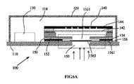
図1は本発明の一実施形態によるMEMSデバイスの断面図である。図1に示すように、MEMSデバイス100は、その中に形成されたサウンドホール112を有するプリント回路基板(PCB)110と、カバー120と、ASICチップ130と、トランスジューサ140及びシャッタ構造150とを含む。カバー120は、プリント回路基板110に取り付けられて囲まれたハウジングを形成し、該ハウジングは内部素子を保護する。ASICチップ130、トランスジューサ140及びシャッタ構造150はハウジングの内部に設置される。シャッタ構造150は、サウンドホール112に取り囲まれるようにPCB110の上方に設置されることができる。トランスジューサ140は、PCB110の上方に設置され、シャッタ構造150の上に位置する。シャッタ構造150はハウジングに連結され音響トランスジューサ140のための音響チャンバ114を形成する。
FIG. 1 is a cross-sectional view of a MEMS device according to an embodiment of the present invention. As shown in FIG. 1, the
図2は本発明の一実施形態による図1に示すMEMSデバイスに応用されるシャッタ構造の一部の斜視図である。図3は図2におけるシャッタ構造の可動部品の上面図である。図1〜図3に示すように、シャッタ構造150は、基板152、スペーサ154及び可動部品156を含む。基板152は通気孔1521を有する。スペーサ154は側壁1541により囲まれた中空空間1543を有する。可動部品156は、固定部1561、可動部1563及びストリップ1565を含むことができる。一実施形態において、固定部1561から可動部1563に延伸するストリップ1565を形成するために、複数の開口溝1564は可動部品156に形成されることができる。例えば、エッチング工程、切断工程などの工程を採用し予め定義されたパターンで板をエッチングすることにより、固定部1561、可動部1563及びストリップ1565を形成することができる。可動部1563の移動及び空気の流れが可動部品156を通過できるという目的を実現するために、開口溝1564とストリップ1565を介して可動部1563と固定部1562を仕切る。可動部1563の寸法は、可動部1563が移動でき(又は曲げて)スペーサ154の中空空間1543を通過できるように設計される。固定部1561と可動部1563の間に位置するストリップ1565は、可動部の柔軟性を向上させ、可動部1563の機械的強度を低下させることができる。
FIG. 2 is a perspective view of a part of a shutter structure applied to the MEMS device shown in FIG. 1 according to an embodiment of the present invention. FIG. 3 is a top view of the movable part having the shutter structure in FIG. As shown in FIGS. 1 to 3, the
スペーサ154は基板152に設置される。可動部品156の固定部1561はスペーサ154の側壁1541に設置され(図1参照)、そのため、可動部1563はスペーサ154の中空空間1543(図1参照)の上方に吊り下がっている。適切な外力が可動部1563に印加された場合、可動部1563は基板152に向かって移動して中空空間1543を通過することができる。
The
図1に戻って、通常の音圧で、可動部品156の開口溝1564、中空空間1543及び通気孔1521が存在するため、空気の流れはサウンドホール112からシャッタ構造150を通過して音響チャンバ114に入ることができ、MEMSの性能に影響を与えることがない。比較的に高い音圧又は空気の流れの衝撃のみで可動部1563の大きな移動を引き起こせることによって音響チャンバへの空気の流れの経路を閉塞することができ、よってMEMSデバイスのダイヤフラムとバックプレートを保護することができる。
Returning to FIG. 1, since the
図4Aと図4Bは本発明の実施形態によるシャッタ構造の動作原理を示す図である。シャッタ構造150は、可動部品156、可動部品156に設置されたスペーサ154及びスペーサ154に設置された基板152を含む。図4Aに示すように、通常の音圧で、可動部品はレスト位置(又は開放位置)に保持されることにより、空気の流れが可動部品156における二つの空気隙間、スペーサ154の開口及び基板152の通気孔を通過することを許可する。更に、図4Bに示すように、高い音圧で、可動部品156の可動部は上方向へ閉鎖位置まで移動することにより、基板152の通気孔を閉塞し、よって空気の流れは通気孔を通過することができない。シャッタ構造の可動部はガス流路に使用されるバルブに類似するため、このような空気の流れを制御する機構はバルブ機構とも称される。
4A and 4B are diagrams illustrating an operation principle of the shutter structure according to the embodiment of the present invention. The
図2に示されたシャッタ構造150がPCB110に取り付けられた場合、常圧で空気の流れがサウンドホール112から通気孔1521に流れることができるように、可動部品156の可動部1563とPCB110の間には一定の空間が控えすべきである。図1に示すように、PCB110の上部をエッチングすることによってサウンドホール112に対して開放された凹溝116を形成することができる。可動部品156の固定部1561はPCB110の凹溝116を取り囲む表面と接触することができ、可動部品156の可動部1563は凹溝116の上方に吊り下がる。そのため、空気の流れ又は音響エネルギーの経路は、サウンドホール112から始まり、凹溝116、中空空間1543及び基板152の通気孔1521を通過してチャンバ115に至ってもよい。好ましくは、凹溝の寸法は可動部1563の凹溝116内での移動を許可するように選ばれることができる。好ましくは、シャッタ構造150は、貫通孔を有する支持部材を介してPCB110に設置されることにより、サウンドホール112から基板152の通気孔1521に流れる空気の流れ及び可動部1563の支持部材の貫通孔内での移動を許可することができる。
When the
シャッタ構造150は音響学的及び機械的に環境に応答している。例えば、落下試験による高い気圧パルス、高い音圧、高い加速度振動(例えば機械的衝撃)などの激しい条件によってMEMSデバイスに用いられる高圧を発生することができる。マイクロフォンの技術分野又はMEMS技術分野に関連する用語である「高圧」とは、MEMSデバイスの内部部品(例えば、MEMSパッケージにおける割れやすいダイヤフラム、バックプレート、カンチレバーとその他の可動構造)に潜在的又は実質的損傷を与えることができる圧力を指すということを理解すべきである。
The
例えば、MEMSデバイスに落下試験による高い気圧パルスが与えられる場合、本発明のMEMSデバイスに用いられるシャッタ構造150の可動部1563は基板152に向かって移動することができる。一般的に、標準大気圧の約1.2倍を超える気圧が本発明のMEMSデバイスに印加される場合、可動部1563は閉鎖位置に移動して基板152の通気孔1521を閉塞することができ、このため、外部環境から音響チャンバへの空気の流れの経路を閉鎖する。
For example, when a high atmospheric pressure pulse by a drop test is given to the MEMS device, the
また、通常の音圧で、シャッタ構造150は開放され、MEMSデバイスは正常に動作し、MEMSデバイスはいかなる影響を受けない。しかしながら、MEMSデバイスに高い音圧が印加される場合、例えば通常の音圧レベルの約500倍を超える音圧が印加される場合、可動部品156の可動部は移動し基板152の通気孔1521を閉塞することができるため、空気の流れの経路を閉鎖してMEMSデバイスが衝撃又は影響を受けないように保護されている。
Also, at normal sound pressure, the
続いて、このような激しい条件が消えた場合、可動部に印加される外力がなくなり、バネの作用により可動部1563は初期位置に戻って空気の流れの経路を開放し、そのため、MEMSは通常の動作状態に戻る。
Subsequently, when such a severe condition disappears, the external force applied to the movable part disappears, and the
そして、高い内部空気圧が発生して可動部品156の可動部1563に印加されると、可動部はPCB110に向かって移動する。そして、内部空気圧が十分に高い場合、可動部1563は移動しPCB110のサウンドホール112を閉塞することができ、よって空気の流れの経路を閉鎖する。
When a high internal air pressure is generated and applied to the
図5は本発明の実施形態による別のMEMSデバイスの断面図である。図5に示すように、MEMSデバイス100は、PCB110、及びその中に形成されたサウンドホール122を有するカバー120を含む。カバー120はPCB110に取り付けられて囲まれたハウジングを形成する。ASICチップ130とトランスジューサ140は前記ハウジングの内部に位置し、PCB110に設置される。シャッタ構造150もハウジングの内部に設置される。しかしながら、シャッタ構造150は、PCB110ではなく、支持部材128を介してサウンドホール122を取り囲んでカバー120に配置される。シャッタ構造150はハウジングに連結されチャンバ114を形成する。支持部材28は、金属板、プラスチック板、バルクシリコン、ボンディングパッド、半田バンプなどであってもよい。好ましくは、図2と図3に示されたシャッタ構造150は、例えばウェハ接合の工程により本実施形態のMEMSデバイスに適用されることができる。
FIG. 5 is a cross-sectional view of another MEMS device according to an embodiment of the present invention. As shown in FIG. 5, the
常圧で、空気の流れは、サウンドホール122、シャッタ構造150に存在する空間及びシャッタ構造150における基板152の通気孔1521を流れることができる。しかしながら、高圧で、シャッタ構造150の可動部1563は、閉鎖位置に移動し基板152の通気孔1521を閉塞することにより、ハウジングの内部に位置するトランスジューサがチャンバ114に進入する強い空気の流れにより損傷されることを防止する。
At normal pressure, the air flow can flow through the
図6Aと図6Bは本発明の実施例によるまた別のMEMSデバイスの断面図を示す。図6Aに示すように、MEMSデバイス100は、PCB110とPCB110に取り付けられたカバー120により構成されるハウジングと、ASICチップ130と、ダイヤフラム142とバックプレート144を有するトランスジューサ140、及びハウジングの内部に設置されたシャッタ構造150とを含む。シャッタ構造150は、PCB110に設置されPCB110のサウンドホール112を取り囲んで設置され、ハウジングとともに使用され音響チャンバ114を形成する。ASICチップ130は、PCB110のシャッタ構造150に近接する位置に設置される。トランスジューサ140は、シャッタ構造150の上方に設置される。シャッタ構造150は、基板152、スペーサ154及び可動部品156を含む。基板152は通気孔1521を有し、スペーサ154は側壁と側壁により囲まれた開口を有し、可動部品156は固定部1561、固定部1561に接続された可動部1563及び固定部1561と可動部1563の間に形成された少なくとも一つの空気隙間を有する。スペーサ154は可動部品156に設置され、基板152はスペーサ154に設置される。図6Aに示すように、スペーサ154は開口を有するため、基板152と可動部品156の間には空間が形成されている。
6A and 6B show cross-sectional views of another MEMS device according to an embodiment of the present invention. As shown in FIG. 6A, the
当該実施例において、可動部品156の固定部はPCB110に直接に設置されることができる。固定部1561は可動部1563より厚いため、可動部1563はサウンドホール112の上方に吊り下がれ、シャッタ構造150の可動部1563とPCB110の間に空間を形成させることができ、よって空気の流れが可動部品156を流れることを許可する。好ましくは、常圧で、可動部1563はPCB110に平行することができる。図1に示されたMEMSデバイスと同様に、常圧で、シャッタ構造150の可動部1563は開放位置に位置して空気の流れの経路を開放し、そのため、空気の流れ又は音声はサウンドホール112、可動部品156、スペーサ154の開口及び基板152の通気孔1521により構成された通気道を通過してチャンバ114に入ることができる。しかしながら、サウンドホール112からの強い空気パルスがシャッタ構造150(図6B参照)を流れると、強い空気パルスによる外力のため、可動部1563は上方向へ曲げ又は移動して基板152の通気孔1521を閉塞する。この場合、MEMSデバイスの空気入口は閉鎖される。可動部品から外力が除去された場合、可動部は初期位置に戻って、MEMSデバイスの空気入口を開放する。
In this embodiment, the fixed part of the
図7Aは本発明の実施形態によるMEMSデバイスに応用される別のシャッタ構造の断面図を示す。図7Aに示すように、シャッタ構造60は、基板層602、スペーサ層604及び可動板層606を含むことができる。スペーサ層604は可動板層606に設置され、基板層602はスペーサ層604に設置される。図7B〜7Dはそれぞれ図7Aにおけるシャッタ構造の一層の上面図を示す。図7Bと7Cに示すように、基板層602は4つの貫通孔6021を有し、スペーサ層604は側壁6041により囲まれた開口6043を有する。可動板606は4つのスロット6061と孔6063を有する。各スロット6061は長方形の可動板606の一側に平行するように形成され、孔6063は板606の中央に位置する。可動板606の外周部分はスペーサ604の側壁6041に接続される固定部6065として使用され、可動板606の中央部分は比較的に大きい力の作用で上方向へ曲げ4つの貫通孔6021を被覆するため、可動部6067として使用される。力が除去されると、可動部6067の材料特性の原因で、可動部6067は初期位置に戻る。本発明により提供されるシャッタ構造60は典型的な実装工程により組み立てられる。
FIG. 7A shows a cross-sectional view of another shutter structure applied to a MEMS device according to an embodiment of the present invention. As shown in FIG. 7A, the shutter structure 60 can include a
示された一実施例において、可動板は長さと厚さが約1.1mm、且つ厚さが約20umの穴あきのステンレス鋼板であってもよく、ステンレス鋼板に対して4つのスロット(図7D参照)を切削加工した場合、可動板の可動部のたわみは約20umから約40umであり、激しい条件において十分に可動部6067を上方向へ移動させ4つの貫通孔6021を閉塞する。好ましくは、可動板は硬質プラスチックシート(例えば、PET、PVC)であってもよく、この場合、可動板における溝削りは不必要である。一実施例において、可動板は中央部分に孔6063を有しなくてもよい。孔6063のない板に比べて、穴あき板の音響抵抗は小さく、且つマイクロフォンの低周波応答に対する影響も小さく、これはマイクロフォンデバイスの騒音を低くするが、例えば粒子の外部位置がMEMSマイクロフォンデバイスの内部に落ち込やすくなるという欠陥を有する。
In one embodiment shown, the movable plate may be a perforated stainless steel plate having a length and thickness of about 1.1 mm and a thickness of about 20 um, with four slots (see FIG. 7D) for the stainless steel plate. ), The deflection of the movable portion of the movable plate is about 20 μm to about 40 μm, and the
本発明のシャッタ構造は、金属(例えばアルミニウム)、シリコン、窒化シリコン(Si3N4)、多結晶シリコン、ガラス、セラミックス、PCB、ポリマー、プラスチック、弾性体又は類似体、或いはそれらの組み合わせ物からなることができる。 The shutter structure of the present invention may be made of metal (for example, aluminum), silicon, silicon nitride (Si3N4), polycrystalline silicon, glass, ceramics, PCB, polymer, plastic, elastic body or analog, or a combination thereof. it can.
本発明の実施形態において、MEMSデバイスの実例はハウジングにおける一つのサウンドホールのみ示しているが、MEMSデバイスのハウジングに複数のサウンドホールを形成してもよい。例えば、一つのサウンドホールはPCBに形成され、別のサウンドホールはカバーに形成される。この場合、MEMSデバイスに複数のシャッタ構造を使用することができ、各シャッタ構造は一つのサウンドホールを取り囲んで設置することができる。これらのシャッタ構造は、MEMSデバイスにおけるダイヤフラムとその他の可動構造が高い音圧又は強い空気の流れで大きく変形することを阻止することができる。 In the embodiment of the present invention, the MEMS device example shows only one sound hole in the housing, but a plurality of sound holes may be formed in the housing of the MEMS device. For example, one sound hole is formed on the PCB and another sound hole is formed on the cover. In this case, a plurality of shutter structures can be used in the MEMS device, and each shutter structure can be installed surrounding one sound hole. These shutter structures can prevent the diaphragm and other movable structures in the MEMS device from being greatly deformed by high sound pressure or strong air flow.
本発明の好ましい実施形態において、シャッタ構造はハウジングの外部に設置されることができ、例えば、PCB110のサウンドホール112を取り囲む外表面に設置することができる。このような実施例において、シャッタ構造は、側壁により囲まれた開口を有するスペーサと可動部品を含むことができ、少なくとも一つの通気孔を有する基板を省略することができる。シャッタ構造のスペーサはPCB110の外表面に接合され、サウンドホールを取り囲むことができ、可動部品はスペーサに設置されることができる。常圧で、シャッタ構造の可動部は開放位置に保持されることにより、空気の流れ又は音響エネルギーがシャッタ構造とサウンドホールにより構成される経路を通過してハウジングの内部に入るようにすることができ、激しい条件において、可動部品の可動部は上方向へ移動し(又は曲げ)サウンドホールを閉塞し、よって空気の流れの経路を閉鎖することができる。
In a preferred embodiment of the present invention, the shutter structure can be installed outside the housing, for example, on the outer surface surrounding the
同様に、一実施形態において、カバーが一つのサウンドホールを有する場合、シャッタ構造は前記サウンドホールを取り囲んでカバーの外表面に設置される。 Similarly, in one embodiment, when the cover has one sound hole, the shutter structure is installed on the outer surface of the cover so as to surround the sound hole.
好ましい実施例において、シャッタ構造の可動部品とスペーサは2つの独立した部品ではなく、一体構造に構成されることができる。例えば、可動部品の外周部分に沿って突出部を形成することによって可動部品の可動部が基板に向かって移動する時に可動部を収容する開口が形成される。別の好ましい実施例において、可動部品、スペーサ及び基板は一体構造に構成されることができる。また別の好ましい実施例において、可動部品の可動部は互いに空気隙間により仕切られた可動バーのアレイであってもよい。 In a preferred embodiment, the movable part and the spacer of the shutter structure can be constructed in one piece rather than two separate parts. For example, by forming the protruding portion along the outer peripheral portion of the movable component, an opening for accommodating the movable portion is formed when the movable portion of the movable component moves toward the substrate. In another preferred embodiment, the movable part, the spacer and the substrate can be constructed in one piece. In another preferred embodiment, the movable part of the movable part may be an array of movable bars separated from each other by an air gap.
好ましくは、本発明により提供されるシャッタ構造とトランスジューサ素子により、独立した市販のデバイスに構成されることができる。シャッタ構造は独立したトランスジューサ素子に取り付けられ、トランスジューサ素子のダイヤフラムはシャッタ構造の基板に臨む。シャッタ構造は更にCMOSモノリシック集積型マイクロフォンデバイスに応用されることができる。シャッタ構造は更に絶縁体におけるシリコン(SOI)ウェハに適用されることにより、MEMSマイクロフォンデバイスと異なるMEMSデバイスを形成することができる。そして、本発明によるシャッタ構造はウェハ接合工程によりMEMSデバイスに応用されることもできる。 Preferably, the shutter structure and the transducer element provided by the present invention can be configured as an independent commercially available device. The shutter structure is attached to an independent transducer element, and the diaphragm of the transducer element faces the shutter structure substrate. The shutter structure can also be applied to CMOS monolithic integrated microphone devices. The shutter structure can also be applied to a silicon (SOI) wafer in an insulator to form a MEMS device that is different from the MEMS microphone device. The shutter structure according to the present invention can be applied to a MEMS device by a wafer bonding process.
以上のように本発明の実施形態及びその優位性を詳細に説明したが、特許請求の範囲に限定された趣旨と範囲を逸脱しない限り、本明細書に対して様々な変形、置換及び変更を行うことができることを理解すべきである。 As described above, the embodiments of the present invention and the advantages thereof have been described in detail. However, various modifications, substitutions, and changes may be made to the present specification without departing from the spirit and scope limited to the claims. It should be understood that it can be done.
また、本出願の範囲は明細書に記載された工程、設備、製造、及びイベント、態様、方法とステップにより構成された具体的な実施形態を限定するためのものではない。当業者は、開示文献に基づいて、現在示された又は後に開発される基本的に同じ機能を実行する又は本明細書を実現するために利用できる前述の対応する実施形態結果が基本的に同じである開示文献、工程、設備、製造、及びイベント、態様、方法とステップの構成を容易に理解できるであろう。従って、添付の特許請求の範囲は、こられの工程、設備、製造、及びイベント、態様、方法とステップの構成の範囲内に含まれるべきである。 In addition, the scope of the present application is not intended to limit specific embodiments configured by processes, equipment, manufacturing, and events, aspects, methods, and steps described in the specification. Based on the disclosure literature, those skilled in the art will perform essentially the same functions currently shown or later developed, or the results of the corresponding embodiments described above that can be used to realize the present specification are basically the same. The disclosure literature, processes, equipment, manufacturing, and events, aspects, methods and steps of the present invention will be easily understood. Accordingly, the appended claims are to be embraced within the scope of these processes, facilities, manufacture, and events, aspects, methods and steps.
Claims (19)
前記プリント回路基板に取り付けられ、ハウジングを形成するカバーと、
前記ハウジングに形成された少なくとも一つのサウンドホールと、
前記ハウジングの内部に位置し、ダイヤフラムを有するトランスジューサと、
前記ハウジングの内部に位置し、それぞれ対応する前記サウンドホールを取り囲んで前記ハウジングに装着される少なくとも一つのシャッタ構造と、
を備えるMEMSデバイスであって、
前記シャッタ構造は、
その中に形成された少なくとも一つの通気孔を有する基板と、
その中に形成された少なくとも一つの空気隙間と可動部を有し、前記基板と前記ハウジングの間に接続された可動部品と、
をそれぞれに備え、
前記可動部は、
常圧で、前記サウンドホールから前記可動部品の少なくとも一つの空気隙間を介して前記基板の少なくとも一つの通気孔に至る空気の流れの経路が開放されるように、開放位置に保持され、
高い外圧で、第1閉鎖位置に移動することにより、前記基板の少なくとも一つの通気孔を閉塞して、前記空気の流れの経路を閉鎖する
ことを特徴とするMEMSデバイス。 A printed circuit board;
A cover attached to the printed circuit board and forming a housing;
At least one sound hole formed in the housing;
A transducer located within the housing and having a diaphragm;
At least one shutter structure located inside the housing and surrounding the corresponding sound hole and mounted on the housing;
A MEMS device comprising:
The shutter structure is
A substrate having at least one vent formed therein;
A movable part having at least one air gap and a movable part formed therein, and connected between the substrate and the housing;
For each
The movable part is
At normal pressure, it is held in an open position so that an air flow path from the sound hole through at least one air gap in the movable part to at least one vent hole in the substrate is opened.
The MEMS device, wherein the air flow path is closed by closing at least one vent hole of the substrate by moving to a first closed position with a high external pressure.
前記少なくとも一つのシャッタ構造は、前記第1サウンドホールに対応し、前記プリント回路基板の第1サウンドホールの上方に設置された第1シャッタ構造を含み、
前記トランスジューサは、前記第1シャッタ構造の基板に設置されることを特徴とする請求項1に記載のMEMSデバイス。 The at least one sound hole includes a first sound hole formed in the printed circuit board;
The at least one shutter structure includes a first shutter structure corresponding to the first sound hole and disposed above the first sound hole of the printed circuit board;
The MEMS device according to claim 1, wherein the transducer is installed on a substrate having the first shutter structure.
前記少なくとも一つのシャッタ構造は、前記第2サウンドホールに対応し、その可動部品が前記カバーの内表面に接合され、前記第2サウンドホールの上方に位置する第2シャッタ構造を含み、
前記トランスジューサは、前記プリント回路基板の上方に設置されることを特徴とする請求項1に記載のMEMSデバイス。 The at least one sound hole includes a second sound hole formed in the cover;
The at least one shutter structure includes a second shutter structure corresponding to the second sound hole, a movable part of which is joined to an inner surface of the cover, and located above the second sound hole;
The MEMS device according to claim 1, wherein the transducer is installed above the printed circuit board.
前記可動部は前記基板に平行し、
前記第1スペーサは、前記基板と前記可動部品の間に接続され、常圧では、空気の流れが前記第1開口を通過して前記少なくとも一つの通気口に至ることを許可し、前記高い外圧で、前記第1開口を通じて前記可動部が移動することを許可する、ことを特徴とする請求項1に記載のMEMSデバイス。 The shutter structure further includes a first spacer having a first opening surrounded by a sidewall,
The movable part is parallel to the substrate;
The first spacer is connected between the substrate and the movable part, and at normal pressure, allows an air flow to pass through the first opening to reach the at least one vent, and the high external pressure. The MEMS device according to claim 1, wherein the movable portion is allowed to move through the first opening.
前記第1シャッタ構造は前記凹溝を取り囲んで設置され、前記可動部品の可動部は前記凹溝の上方に吊り下がっていることを特徴とする請求項2に記載のMEMSデバイス。 A concave groove that opens to the first sound hole is formed on the printed circuit board.
3. The MEMS device according to claim 2, wherein the first shutter structure is disposed so as to surround the concave groove, and a movable part of the movable part is suspended above the concave groove. 4.
前記少なくとも一つの空気隙間は、前記固定部と前記可動部を仕切り、前記可動部は前記可動部品の中心部に位置することを特徴とする請求項1〜請求項4のいずれかに記載のMEMSデバイス。 The movable part further includes a fixed part connected to the substrate, and the fixed part is located at a peripheral edge of the movable part,
5. The MEMS according to claim 1, wherein the at least one air gap partitions the fixed portion and the movable portion, and the movable portion is located at a central portion of the movable component. device.
前記可動部品は、前記固定部と前記可動部の間に接続されるバネを更に含んで、前記高い外圧での前記可動部の移動を促進することを特徴とする請求項7に記載のMEMSデバイス。 The movable part of the movable part is a perforated plate communicating with the sound hole and the at least one vent hole, and / or
The MEMS device according to claim 7, wherein the movable part further includes a spring connected between the fixed part and the movable part to promote movement of the movable part at the high external pressure. .
前記プリント回路基板に取り付けられ、ハウジングを形成するカバーと、
前記ハウジングに形成された第1貫通孔と、
可動部、支持部及び前記可動部と前記支持部の間に形成された少なくとも一つの空気隙間を有するシャッタ構造と、
を備えるMEMSデバイスであって、
前記シャッタ構造は、前記第1貫通孔を取り囲んで設置され、前記支持部を介して前記ハウジングに接合されることにより、前記第1貫通孔から前記シャッタ構造の少なくとも一つの空気隙間を通過して前記ハウジングの内部に至る空気の流れの経路を提供し、
前記シャッタ構造の可動部は、
常圧で、前記空気の流れの経路を開放するように、開放位置に保持され、
高圧で、閉鎖位置に移動することにより、前記空気の流れの経路を閉鎖し、
前記シャッタ構造は前記ハウジングの内表面に接合され、
前記シャッタ構造の支持部は、少なくとも一つの通気孔を有し前記可動部に平行する基板を含み、
前記シャッタ構造は、側壁により密閉された第2開口を有する第2スペーサを含み、
前記第2スペーサは、前記基板と前記可動部の間に接続されることにより、常圧で空気の流れが順に前記第1貫通孔、前記少なくとも一つの空間隙間、前記第2開口及び前記少なくとも一つの通気孔を通過して前記ハウジングの音響チャンバに入ることができ、且つ、高圧で可動部が基板に向かって移動し前記第2開口を通過することにより、前記少なくとも一つの通気孔を閉塞することができることを特徴とするMEMSデバイス。 A printed circuit board and a cover attached to the printed circuit board and forming a housing;
A first through hole formed in the housing;
A movable portion, a support portion, and a shutter structure having at least one air gap formed between the movable portion and the support portion;
A MEMS device comprising:
The shutter structure is installed so as to surround the first through hole, and is joined to the housing through the support portion so as to pass through at least one air gap of the shutter structure from the first through hole. Providing an air flow path to the interior of the housing;
The movable part of the shutter structure is
Held at an open position so as to open the air flow path at normal pressure,
Closing the air flow path by moving to a closed position at high pressure ,
The shutter structure is joined to the inner surface of the housing;
The support portion of the shutter structure includes a substrate having at least one vent hole and parallel to the movable portion,
The shutter structure includes a second spacer having a second opening sealed by a side wall;
The second spacer is connected between the substrate and the movable part, so that air flows in order at normal pressure in the order of the first through hole, the at least one space gap, the second opening, and the at least one. The at least one vent hole is closed by passing through one vent hole and entering the acoustic chamber of the housing and moving the movable part toward the substrate at high pressure and passing through the second opening. MEMS device, characterized in that it is possible.
前記高圧で、前記シャッタ構造の可動部は前記第1開口部を通じて前記閉鎖位置に移動して、前記第1貫通孔を閉塞することを特徴とする請求項13に記載のMEMSデバイス。 The shutter structure is joined to the outer surface of the housing via a first spacer having a first opening surrounded by a side wall,
14. The MEMS device according to claim 13, wherein the movable part of the shutter structure moves to the closed position through the first opening at the high pressure to close the first through hole.
シャッタ構造と、
を備える音響トランスジューサデバイスであって、
前記シャッタ構造は、
その中に形成された少なくとも一つの孔を有する基板と、
その中に形成された少なくとも一つの空気隙間と可動部を有する可動部品と
を備え、
前記可動部品と前記基板の間に囲まれた空間が形成されるように、前記可動部品は前記基板の第1表面に接合され、
前記トランスジューサ素子は、前記基板の第2表面に接合され、前記トランスジューサ素子のダイヤフラムは前記第1表面に対向する前記第2表面に面し、
前記可動部は、常圧でレスト位置に保持されることにより、可動部品の少なくとも一つの空気隙間から前記基板の少なくとも一つの孔を通過して前記トランスジューサ素子のダイヤフラムに至る空気の流れの経路を提供し、高圧で前記囲まれた空間を通じて基板に向かって移動することにより、前記基板の少なくとも一つの孔を閉塞することを特徴とする音響トランスジューサデバイス。 A transducer element having a diaphragm;
A shutter structure;
An acoustic transducer device comprising:
The shutter structure is
A substrate having at least one hole formed therein;
Comprising at least one air gap formed therein and a movable part having a movable part,
The movable component is bonded to the first surface of the substrate so that a space surrounded by the movable component and the substrate is formed,
The transducer element is bonded to a second surface of the substrate, and the diaphragm of the transducer element faces the second surface opposite the first surface;
The movable part is held at a rest position at normal pressure, thereby passing an air flow path from at least one air gap of the movable part through the at least one hole of the substrate to the diaphragm of the transducer element. An acoustic transducer device is provided that closes at least one hole in the substrate by moving toward the substrate through the enclosed space at high pressure.
Applications Claiming Priority (1)
| Application Number | Priority Date | Filing Date | Title |
|---|---|---|---|
| PCT/CN2014/085274 WO2016029378A1 (en) | 2014-08-27 | 2014-08-27 | Mems device with valve mechanism |
Publications (2)
| Publication Number | Publication Date |
|---|---|
| JP2017530659A JP2017530659A (en) | 2017-10-12 |
| JP6445158B2 true JP6445158B2 (en) | 2018-12-26 |
Family
ID=55398593
Family Applications (1)
| Application Number | Title | Priority Date | Filing Date |
|---|---|---|---|
| JP2017527956A Active JP6445158B2 (en) | 2014-08-27 | 2014-08-27 | MEMS device with valve mechanism |
Country Status (5)
| Country | Link |
|---|---|
| US (1) | US10212501B2 (en) |
| EP (1) | EP3186979A4 (en) |
| JP (1) | JP6445158B2 (en) |
| CN (1) | CN105493519B (en) |
| WO (1) | WO2016029378A1 (en) |
Cited By (1)
| Publication number | Priority date | Publication date | Assignee | Title |
|---|---|---|---|---|
| US11350220B2 (en) | 2020-01-17 | 2022-05-31 | Sae Magnetics (H.K.) Ltd. | MEMS package, MEMS microphone and method of manufacturing the MEMS package |
Families Citing this family (30)
| Publication number | Priority date | Publication date | Assignee | Title |
|---|---|---|---|---|
| WO2016029378A1 (en) * | 2014-08-27 | 2016-03-03 | Goertek. Inc | Mems device with valve mechanism |
| KR101807040B1 (en) * | 2016-05-26 | 2017-12-08 | 현대자동차 주식회사 | Microphone |
| US9975760B2 (en) * | 2016-06-28 | 2018-05-22 | Robert Bosch Gmbh | MEMS sensor device package housing with an embedded controllable device |
| US10469940B2 (en) * | 2016-09-23 | 2019-11-05 | Apple Inc. | Valve for acoustic port |
| JP6930101B2 (en) * | 2016-12-12 | 2021-09-01 | オムロン株式会社 | Acoustic sensors and capacitive transducers |
| EP3635974A4 (en) * | 2017-06-05 | 2021-03-10 | Robert Bosch GmbH | Microphone with encapsulated moving electrode |
| US10654712B2 (en) * | 2017-09-21 | 2020-05-19 | Knowles Electronics, Llc | Elevated MEMS device in a microphone with ingress protection |
| CN111108758B (en) * | 2017-09-22 | 2022-01-18 | 罗伯特·博世有限公司 | MEMS microphone system |
| US10609474B2 (en) | 2017-10-18 | 2020-03-31 | xMEMS Labs, Inc. | Air pulse generating element and manufacturing method thereof |
| US10609463B2 (en) * | 2017-10-30 | 2020-03-31 | Taiwan Semiconductor Manufacturing Co., Ltd. | Integrated microphone device and manufacturing method thereof |
| DE102018200190B4 (en) * | 2018-01-08 | 2019-08-14 | Infineon Technologies Ag | Microelectromechanical system with filter structure |
| US11181627B2 (en) | 2018-02-05 | 2021-11-23 | Denso Corporation | Ultrasonic sensor |
| US10425732B1 (en) * | 2018-04-05 | 2019-09-24 | xMEMS Labs, Inc. | Sound producing device |
| US10771891B2 (en) * | 2018-08-19 | 2020-09-08 | xMEMS Labs, Inc. | Method for manufacturing air pulse generating element |
| CN110958512A (en) * | 2018-09-27 | 2020-04-03 | 北京小米移动软件有限公司 | Microphone module and terminal equipment |
| CN110958541A (en) | 2018-09-27 | 2020-04-03 | 北京小米移动软件有限公司 | Microphone module and terminal |
| CN109379684B (en) * | 2018-10-09 | 2020-05-29 | 歌尔股份有限公司 | Microphone and electronic device |
| JP7211220B2 (en) * | 2019-04-05 | 2023-01-24 | 株式会社デンソー | ultrasonic sensor |
| CN110049419A (en) * | 2019-04-12 | 2019-07-23 | 苏州敏芯微电子技术股份有限公司 | Silicon microphone |
| US10783866B1 (en) * | 2019-07-07 | 2020-09-22 | xMEMS Labs, Inc. | Sound producing device |
| JP7226154B2 (en) | 2019-07-10 | 2023-02-21 | 株式会社デンソー | ultrasonic sensor |
| US11046576B1 (en) * | 2019-12-04 | 2021-06-29 | Motorola Mobility Llc | Pressure relief device for microphone protection in an electronic device and corresponding methods |
| CN111131988B (en) * | 2019-12-30 | 2021-06-18 | 歌尔股份有限公司 | Vibration sensor and audio device |
| CN111757223B (en) * | 2020-06-30 | 2021-12-14 | 瑞声声学科技(深圳)有限公司 | MEMS microphone chip |
| US11778367B2 (en) | 2020-09-25 | 2023-10-03 | Apple Inc. | Impulse pressure rejecting valve for an electronic device |
| DE102021203360A1 (en) | 2021-04-01 | 2022-10-06 | Fraunhofer-Gesellschaft zur Förderung der angewandten Forschung eingetragener Verein | MEMS SOUND TRANSDUCER |
| CN218162856U (en) * | 2021-04-23 | 2022-12-27 | 深圳市韶音科技有限公司 | Vibration sensor |
| CN113905318A (en) * | 2021-09-16 | 2022-01-07 | 歌尔微电子股份有限公司 | Microphone structure |
| EP4206120A1 (en) * | 2021-12-29 | 2023-07-05 | Infineon Technologies AG | Mems device having a mechanical barrier structure |
| WO2023189141A1 (en) * | 2022-03-31 | 2023-10-05 | ソニーグループ株式会社 | Sound reproduction device |
Family Cites Families (28)
| Publication number | Priority date | Publication date | Assignee | Title |
|---|---|---|---|---|
| US5452268A (en) * | 1994-08-12 | 1995-09-19 | The Charles Stark Draper Laboratory, Inc. | Acoustic transducer with improved low frequency response |
| US6324907B1 (en) | 1999-11-29 | 2001-12-04 | Microtronic A/S | Flexible substrate transducer assembly |
| US8623709B1 (en) * | 2000-11-28 | 2014-01-07 | Knowles Electronics, Llc | Methods of manufacture of top port surface mount silicon condenser microphone packages |
| US7434305B2 (en) * | 2000-11-28 | 2008-10-14 | Knowles Electronics, Llc. | Method of manufacturing a microphone |
| US6781231B2 (en) | 2002-09-10 | 2004-08-24 | Knowles Electronics Llc | Microelectromechanical system package with environmental and interference shield |
| GB0605576D0 (en) * | 2006-03-20 | 2006-04-26 | Oligon Ltd | MEMS device |
| JP5237069B2 (en) * | 2008-12-05 | 2013-07-17 | 株式会社オーディオテクニカ | Omnidirectional condenser microphone unit and omnidirectional condenser microphone |
| US8325951B2 (en) * | 2009-01-20 | 2012-12-04 | General Mems Corporation | Miniature MEMS condenser microphone packages and fabrication method thereof |
| CN202178856U (en) * | 2011-08-17 | 2012-03-28 | 瑞声声学科技(深圳)有限公司 | Microphone |
| CN103347808B (en) | 2011-12-29 | 2016-02-10 | 歌尔声学股份有限公司 | Silica-based MEMS microphone, the system comprising this microphone and encapsulation |
| JP5741487B2 (en) * | 2012-02-29 | 2015-07-01 | オムロン株式会社 | microphone |
| US9002037B2 (en) * | 2012-02-29 | 2015-04-07 | Infineon Technologies Ag | MEMS structure with adjustable ventilation openings |
| CN202551279U (en) * | 2012-04-28 | 2012-11-21 | 歌尔声学股份有限公司 | Microphone |
| CN202587316U (en) * | 2012-05-24 | 2012-12-05 | 歌尔声学股份有限公司 | Microphone |
| CN103517169B (en) * | 2012-06-22 | 2017-06-09 | 英飞凌科技股份有限公司 | MEMS structure and MEMS device with adjustable ventilation opening |
| US9078063B2 (en) * | 2012-08-10 | 2015-07-07 | Knowles Electronics, Llc | Microphone assembly with barrier to prevent contaminant infiltration |
| US8724841B2 (en) * | 2012-08-30 | 2014-05-13 | Apple Inc. | Microphone with acoustic mesh to protect against sudden acoustic shock |
| GB2506174A (en) * | 2012-09-24 | 2014-03-26 | Wolfson Microelectronics Plc | Protecting a MEMS device from excess pressure and shock |
| US9137595B2 (en) * | 2012-11-14 | 2015-09-15 | Knowles Electronics, Llc | Apparatus for prevention of pressure transients in microphones |
| US9357299B2 (en) * | 2012-11-16 | 2016-05-31 | Apple Inc. | Active protection for acoustic device |
| US9185480B2 (en) * | 2012-12-14 | 2015-11-10 | Apple Inc. | Acoustically actuated mechanical valve for acoustic transducer protection |
| WO2016029378A1 (en) * | 2014-08-27 | 2016-03-03 | Goertek. Inc | Mems device with valve mechanism |
| GB2533410B (en) * | 2014-12-19 | 2017-03-01 | Cirrus Logic Int Semiconductor Ltd | MEMS devices and processes |
| CN107211222B (en) * | 2015-01-26 | 2020-03-24 | 思睿逻辑国际半导体有限公司 | MEMS transducer |
| US9794661B2 (en) * | 2015-08-07 | 2017-10-17 | Knowles Electronics, Llc | Ingress protection for reducing particle infiltration into acoustic chamber of a MEMS microphone package |
| GB2556280B (en) * | 2016-01-28 | 2020-05-27 | Cirrus Logic Int Semiconductor Ltd | MEMS device and process |
| GB2546827B (en) * | 2016-01-28 | 2020-01-29 | Cirrus Logic Int Semiconductor Ltd | MEMS device and process |
| GB2560774B (en) * | 2017-03-24 | 2019-11-13 | Cirrus Logic Int Semiconductor Ltd | MEMS devices and processes |
-
2014
- 2014-08-27 WO PCT/CN2014/085274 patent/WO2016029378A1/en active Application Filing
- 2014-08-27 CN CN201480037351.8A patent/CN105493519B/en active Active
- 2014-08-27 US US15/505,001 patent/US10212501B2/en active Active
- 2014-08-27 JP JP2017527956A patent/JP6445158B2/en active Active
- 2014-08-27 EP EP14900342.8A patent/EP3186979A4/en not_active Withdrawn
Cited By (1)
| Publication number | Priority date | Publication date | Assignee | Title |
|---|---|---|---|---|
| US11350220B2 (en) | 2020-01-17 | 2022-05-31 | Sae Magnetics (H.K.) Ltd. | MEMS package, MEMS microphone and method of manufacturing the MEMS package |
Also Published As
| Publication number | Publication date |
|---|---|
| EP3186979A1 (en) | 2017-07-05 |
| CN105493519B (en) | 2020-08-25 |
| CN105493519A (en) | 2016-04-13 |
| EP3186979A4 (en) | 2018-02-28 |
| JP2017530659A (en) | 2017-10-12 |
| WO2016029378A1 (en) | 2016-03-03 |
| US10212501B2 (en) | 2019-02-19 |
| US20170280218A1 (en) | 2017-09-28 |
Similar Documents
| Publication | Publication Date | Title |
|---|---|---|
| JP6445158B2 (en) | MEMS device with valve mechanism | |
| CN106537938B (en) | MEMS acoustic transducer with stopper mechanism and acoustic transducer device | |
| US11059716B2 (en) | Directional microphone and associated packing techniques | |
| TWI616104B (en) | Reduced footprint microphone system with spacer member having through-hole | |
| US9338559B2 (en) | Microphone system with a stop member | |
| US8447054B2 (en) | Microphone with variable low frequency cutoff | |
| US20200137501A1 (en) | Mems devices and processes | |
| US9137595B2 (en) | Apparatus for prevention of pressure transients in microphones | |
| WO2018064803A1 (en) | Mems microphone device and electronics apparatus | |
| KR101452396B1 (en) | Mems microphone having multiple sound pass hole | |
| WO2018064804A1 (en) | Mems device and electronics apparatus | |
| CN110679159B (en) | Microphone with encapsulated moving electrode | |
| CN101010983A (en) | Silicon based condenser microphone and mounting method for the same | |
| CN112788508B (en) | Structure of micro-electromechanical system microphone and manufacturing method thereof | |
| EP3334184B1 (en) | Acoustic sensor and capacitive transducer | |
| CN109309884B (en) | Microphone and electronic equipment | |
| KR101496192B1 (en) | Mems microphone having piezo membrane | |
| CN208739421U (en) | A kind of sensor device | |
| KR101452402B1 (en) | Mems microphone having sound pass hole by downward curve | |
| KR101496200B1 (en) | Mems microphone having multiple diaphragm | |
| TWI665153B (en) | Stress decoupling in mems transducers |
Legal Events
| Date | Code | Title | Description |
|---|---|---|---|
| A131 | Notification of reasons for refusal |
Free format text: JAPANESE INTERMEDIATE CODE: A131 Effective date: 20180424 |
|
| A601 | Written request for extension of time |
Free format text: JAPANESE INTERMEDIATE CODE: A601 Effective date: 20180723 |
|
| A521 | Request for written amendment filed |
Free format text: JAPANESE INTERMEDIATE CODE: A523 Effective date: 20180925 |
|
| TRDD | Decision of grant or rejection written | ||
| A01 | Written decision to grant a patent or to grant a registration (utility model) |
Free format text: JAPANESE INTERMEDIATE CODE: A01 Effective date: 20181113 |
|
| A61 | First payment of annual fees (during grant procedure) |
Free format text: JAPANESE INTERMEDIATE CODE: A61 Effective date: 20181128 |
|
| R150 | Certificate of patent or registration of utility model |
Ref document number: 6445158 Country of ref document: JP Free format text: JAPANESE INTERMEDIATE CODE: R150 |
|
| S111 | Request for change of ownership or part of ownership |
Free format text: JAPANESE INTERMEDIATE CODE: R313113 |
|
| R350 | Written notification of registration of transfer |
Free format text: JAPANESE INTERMEDIATE CODE: R350 |
|
| R250 | Receipt of annual fees |
Free format text: JAPANESE INTERMEDIATE CODE: R250 |
|
| R250 | Receipt of annual fees |
Free format text: JAPANESE INTERMEDIATE CODE: R250 |
|
| R250 | Receipt of annual fees |
Free format text: JAPANESE INTERMEDIATE CODE: R250 |