EP2386840A2 - Acoustic sensor - Google Patents
Acoustic sensor Download PDFInfo
- Publication number
- EP2386840A2 EP2386840A2 EP11161591A EP11161591A EP2386840A2 EP 2386840 A2 EP2386840 A2 EP 2386840A2 EP 11161591 A EP11161591 A EP 11161591A EP 11161591 A EP11161591 A EP 11161591A EP 2386840 A2 EP2386840 A2 EP 2386840A2
- Authority
- EP
- European Patent Office
- Prior art keywords
- electrode film
- diaphragm
- back plate
- acoustic sensor
- vibration electrode
- Prior art date
- Legal status (The legal status is an assumption and is not a legal conclusion. Google has not performed a legal analysis and makes no representation as to the accuracy of the status listed.)
- Granted
Links
- 230000002093 peripheral effect Effects 0.000 claims abstract description 52
- 239000000758 substrate Substances 0.000 claims description 40
- 239000004065 semiconductor Substances 0.000 claims description 19
- 239000011800 void material Substances 0.000 claims description 6
- 230000001939 inductive effect Effects 0.000 abstract description 2
- 239000010408 film Substances 0.000 description 79
- XUIMIQQOPSSXEZ-UHFFFAOYSA-N Silicon Chemical compound [Si] XUIMIQQOPSSXEZ-UHFFFAOYSA-N 0.000 description 22
- 229910052710 silicon Inorganic materials 0.000 description 22
- 239000010703 silicon Substances 0.000 description 22
- 238000000605 extraction Methods 0.000 description 6
- 230000000694 effects Effects 0.000 description 5
- 229910021420 polycrystalline silicon Inorganic materials 0.000 description 5
- 229920005591 polysilicon Polymers 0.000 description 5
- VYPSYNLAJGMNEJ-UHFFFAOYSA-N Silicium dioxide Chemical compound O=[Si]=O VYPSYNLAJGMNEJ-UHFFFAOYSA-N 0.000 description 4
- 238000000034 method Methods 0.000 description 4
- 230000002829 reductive effect Effects 0.000 description 4
- 239000010409 thin film Substances 0.000 description 4
- 238000009423 ventilation Methods 0.000 description 4
- 239000012790 adhesive layer Substances 0.000 description 3
- 239000003990 capacitor Substances 0.000 description 3
- 238000004519 manufacturing process Methods 0.000 description 3
- 230000001681 protective effect Effects 0.000 description 3
- 229910052681 coesite Inorganic materials 0.000 description 2
- 230000008094 contradictory effect Effects 0.000 description 2
- 229910052906 cristobalite Inorganic materials 0.000 description 2
- 239000000377 silicon dioxide Substances 0.000 description 2
- 229910052682 stishovite Inorganic materials 0.000 description 2
- 229910052905 tridymite Inorganic materials 0.000 description 2
- 230000001133 acceleration Effects 0.000 description 1
- 238000004140 cleaning Methods 0.000 description 1
- 230000005611 electricity Effects 0.000 description 1
- 230000002708 enhancing effect Effects 0.000 description 1
- 238000005530 etching Methods 0.000 description 1
- 230000002401 inhibitory effect Effects 0.000 description 1
- 239000010410 layer Substances 0.000 description 1
- 239000012811 non-conductive material Substances 0.000 description 1
- 230000002441 reversible effect Effects 0.000 description 1
- 125000006850 spacer group Chemical group 0.000 description 1
- 230000003068 static effect Effects 0.000 description 1
- XLYOFNOQVPJJNP-UHFFFAOYSA-N water Substances O XLYOFNOQVPJJNP-UHFFFAOYSA-N 0.000 description 1
- 238000009736 wetting Methods 0.000 description 1
Images


Classifications
-
- G—PHYSICS
- G01—MEASURING; TESTING
- G01H—MEASUREMENT OF MECHANICAL VIBRATIONS OR ULTRASONIC, SONIC OR INFRASONIC WAVES
- G01H11/00—Measuring mechanical vibrations or ultrasonic, sonic or infrasonic waves by detecting changes in electric or magnetic properties
- G01H11/06—Measuring mechanical vibrations or ultrasonic, sonic or infrasonic waves by detecting changes in electric or magnetic properties by electric means
-
- G—PHYSICS
- G01—MEASURING; TESTING
- G01H—MEASUREMENT OF MECHANICAL VIBRATIONS OR ULTRASONIC, SONIC OR INFRASONIC WAVES
- G01H3/00—Measuring characteristics of vibrations by using a detector in a fluid
-
- H—ELECTRICITY
- H04—ELECTRIC COMMUNICATION TECHNIQUE
- H04R—LOUDSPEAKERS, MICROPHONES, GRAMOPHONE PICK-UPS OR LIKE ACOUSTIC ELECTROMECHANICAL TRANSDUCERS; DEAF-AID SETS; PUBLIC ADDRESS SYSTEMS
- H04R19/00—Electrostatic transducers
- H04R19/005—Electrostatic transducers using semiconductor materials
-
- H—ELECTRICITY
- H04—ELECTRIC COMMUNICATION TECHNIQUE
- H04R—LOUDSPEAKERS, MICROPHONES, GRAMOPHONE PICK-UPS OR LIKE ACOUSTIC ELECTROMECHANICAL TRANSDUCERS; DEAF-AID SETS; PUBLIC ADDRESS SYSTEMS
- H04R19/00—Electrostatic transducers
- H04R19/04—Microphones
-
- H—ELECTRICITY
- H04—ELECTRIC COMMUNICATION TECHNIQUE
- H04R—LOUDSPEAKERS, MICROPHONES, GRAMOPHONE PICK-UPS OR LIKE ACOUSTIC ELECTROMECHANICAL TRANSDUCERS; DEAF-AID SETS; PUBLIC ADDRESS SYSTEMS
- H04R31/00—Apparatus or processes specially adapted for the manufacture of transducers or diaphragms therefor
- H04R31/006—Interconnection of transducer parts
Definitions
- the present invention relates to acoustic sensors, and specifically to a MEMS (Micro Electro Mechanical Systems) type acoustic sensor manufactured using a MEMS technique.
- MEMS Micro Electro Mechanical Systems
- a capacitance type acoustic sensor is disclosed in Japanese Patent No. 4338395 .
- a capacitor is configured by facing a thin film diaphragm and a fixed electrode film arranged in a back plate through a microscopic air gap.
- the gap distance between the diaphragm and the fixed electrode film changes by such vibration, and hence the acoustic vibration can be detected by detecting the change in electrostatic capacitance between the diaphragm and the fixed electrode film.
- the diaphragm In such a capacitance type acoustic sensor, the diaphragm sometimes fixes to the fixed electrode film (hereinafter a state or a phenomenon in which the diaphragm is partially or substantially entirely fixed to the fixed electrode film so that the gap is eliminated is called a stick) in the manufacturing process or during use.
- a state or a phenomenon in which the diaphragm is partially or substantially entirely fixed to the fixed electrode film so that the gap is eliminated is called a stick
- the acoustic vibration cannot be detected by the acoustic sensor since the vibration of the diaphragm is inhibited.
- the cause of sticking in the acoustic sensor is as follows (details in Japanese Unexamined Patent Publication No. 2008-301430 ).
- moisture infiltrates to the air gap between the diaphragm and the fixed electrode film.
- moisture may infiltrates to the air gap between the diaphragm and the fixed electrode film due to humidity and water wetting even during the use of the acoustic sensor.
- the gap distance of the acoustic sensor is only a few micrometers and furthermore, the diaphragm only has a film thickness of about 1 ⁇ m and has a weak spring property.
- the diaphragm gets adsorbed to the fixed electrode film (this is a first stage of sticking) by capillary force or surface tension, and such a sticking state of the diaphragm is held by the inters molecular force, inter-surface force, electrostatic fore and the like acting between the diaphragm and the fixed electrode film even after the moisture has evaporated (this is a second stage of sticking).
- the first stage of sticking may also occur, such as the diaphragm may attach to the fixed electrode film when a large sound pressure or drop impact is applied on the diaphragm thereby greatly displacing the diaphragm, or the diaphragm may attach to the fixed electrode film when charged with static electricity.
- An acoustic sensor in which a great number of stoppers (projections) are arranged on a surface facing the diaphragm of the fixed electrode film to prevent the sticking of the diaphragm is known.
- Such an acoustic sensor is disclosed in Japanese Unexamined Patent Publication No. 2006-157863 , and the like.
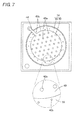
- Fig. 1 and Fig .2 is a plan view and a cross-sectional view each showing an acoustic sensor including a stopper.
- a mode similar to the acoustic sensor of a first embodiment of a conventional example is shown to facilitate the comparison with a first embodiment of the present invention.
- a back chamber 15 passes through from an upper surface to a lower surface of a silicon substrate 12, and a diaphragm 13 of thin film form made of polysilicon is arranged on the upper surface of the silicon substrate 12 to cover an upper surface of the back chamber 15.
- a canopy shaped back plate 14 is fixed to the upper surface of the silicon substrate 12 so as to cover the diaphragm 13.
- the back plate 14 has a fixed electrode film 20 made of polysilicon arranged on a lower surface of a plate portion 19 made of SiN.
- a microscopic air gap is formed between the diaphragm 13 and the fixed electrode film 20, where the diaphragm 13 and the fixed electrode film 20 configure a capacitor.
- a great number of acoustic holes 18 for passing the acoustic vibration are opened in the entire back plate 14.
- a plurality of stoppers 22 each having projection shape of the same length and the same diameter are arranged at substantially equal interval over the entire lower surface of a region facing the diaphragm 13 of the back plate 14.
- each stopper 22 comes into contact with the diaphragm 13 even when the diaphragm 13 is greatly displaced thereby preventing the diaphragm 13 from overly approaching the back plate 14 and inhibiting the sticking of the diaphragm 13.
- the holding force between the diaphragm 13 and the back plate 14 in the second stage of sticking is known to have correlation with a contacting area of the diaphragm 13 and the back plate 14.
- the contacting area of the diaphragm 13 and the stopper 22 becomes large and the holding force of the diaphragm 13 becomes large if the diameter of the stopper 22 is large even if the stopper 22 is arranged on the back plate 14. Therefore, sticking easily occurs if the diameter of the stopper 22 is large even if the stopper 22 is arranged on the back plate 14.
- the stopper 22 is to be arranged on the back plate 14 and the diameter of the stopper 22 is to be preferably made as small as possible to reduce the contacting area of the diaphragm 13 and the back plate 14 in order to prevent sticking of the diaphragm 13.
- the diaphragm 13 hits the stopper 22 when the acoustic sensor 11 is dropped thereby applying a mechanical load on the diaphragm 13. Therefore, if the diameter of the stopper 22 is narrow, a large mechanical load applies on the diaphragm 13 and the diaphragm 13 may easily break when the acoustic sensor 11 is dropped and the diaphragm 13 hits the stopper 22.
- Japanese Unexamined Patent Publication No. 2008-301430 discloses the acoustic sensor in which the interval of the stopper is differed depending on the region to arrange the stopper, but the performance of preventing sticking and the drop resistance property cannot be simultaneously satisfied with such a technique.
- the present invention has been devised to solve the problems described above, and an object thereof is to provide an acoustic sensor in which sticking of the diaphragm can be prevented and also in which the diaphragm is less likely to break by impact when the sensor is dropped.
- an acoustic sensor including a back plate inducing a fixed film arranged on an upper side of a semiconductor substrate and a fixed electrode film arranged on the fixed film, and a vibration electrode film arranged on an upper side of the semiconductor substrate to face the back plate through a void, for converting an acoustic vibration to change in electrostatic capacitance between the vibration electrode film and the fixed electrode film, wherein a plurality of projections are arranged on a surface on the void side of at least one of the back plate and the vibration electrode film, and a cross-sectional area of the projection is differed according to a projection forming region in at least one of the back plate and the vibration electrode film.
- the semiconductor substrate is formed with the hollow portion from the upper surface to the lower side
- the vibration electrode film is arranged on the upper surface of the semiconductor substrate
- the back plate is fixed on the upper surface of the semiconductor substrate so as to cover the vibration electrode film, and a plurality of acoustic holes are opened in the back plate.
- the back plate may be fixed on the upper surface of the semiconductor substrate, and the vibration electrode film may be arranged on the upper side of the back plate.
- a plurality of types of projections having different cross-sectional areas are arranged so that the forming region of the projection having a relatively small cross-sectional area where sticking is less likely to occur and the forming region of the projection having a relatively large cross-sectional area where impact applied on the vibration electrode film can be reduced are differed, so that the sticking of the vibration electrode film can be prevented by optimizing the forming region of the projections having different cross-sectional areas, and the breakage of the vibration electrode film is less likely to occur by the impact when the sensor is dropped.
- the projections are arranged so that the cross-sectional area sequentially becomes smaller toward the outer peripheral side from the center of at least one of the back plate and the vibration electrode film.
- the cross-sectional area of the projection is small in the outer peripheral area where the elastic restoring force when the vibration electrode film is the free end and sticks to the back plate is weak, so that the holding force in the outer peripheral area when the vibration electrode film sticks can be reduced and the sticking of the vibration electrode film is less likely to occur.
- the cross-sectional area of the projection is large at the central part where the vibration electrode film tends to easily hit the back plate the first when receiving the impact or the like, the impact to be applied on the vibration electrode film can be alleviated. Therefore, according to this aspect, the sticking of the vibration electrode film can be prevented and the breakage of the vibration electrode film due to the impact when the sensor is dropped can be prevented.
- the projection having a relatively small cross-sectional area is arranged in the outer peripheral area of at least one of the back plate and the vibration electrode film, and the projection having a relatively large cross-sectional area is arranged in the internal area of at least one of the back plate and the vibration electrode film.
- the cross-sectional area of the projection is small in the outer peripheral area where the elastic restoring force when the vibration electrode film is a free end and sticks to the back plate is weak, so that the holding force in the outer peripheral area when the vibration electrode film sticks can be reduced and sticking is less likely to occur.
- the cross-sectional of the projection is large in the internal where the vibration electrode film tends to easily hit the back plate the first when receiving the impact or the like, the impact to be applied on the vibration electrode film can be alleviated. Therefore, according to this aspect, the sticking of the vibration electrode film can be prevented and the breakage of the vibration electrode film due to the impact when the sensor is dropped can be prevented.
- the width of the outer peripheral area where the projection having a relatively small cross-sectional area is arranged is preferably smaller than or equal to 1/4 of the width of the back plate or the vibration electrode film. If the width of the outer peripheral area is greater 1/4, the vibration electrode film may be in contact with the projection having a small cross-sectional area and break when impact is applied, and hence the impact resistance may be affected.
- the vibration electrode film is arranged on the upper surface of the semiconductor substrate and the back plate is arranged on the upper surface of the semiconductor substrate so as to cover the vibration electrode film
- a plurality of projections are arranged in a region facing the upper surface of the semiconductor substrate of the lower surface of the vibration electrode film, and the cross-sectional area of the projection arranged at the outer peripheral part of the region may be smaller than the cross-sectional area of the projection arranged at the inner peripheral part of the region.
- the means for solving the problems of the invention has a characteristic of appropriately combining the configuring elements described above, and the present invention enables a great number of variations by the combination of the configuring elements.
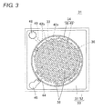
- Fig. 3 is a plan view showing the acoustic sensor 31 of the first embodiment.
- Fig. 4 is a cross-sectional view of the acoustic sensor 31.
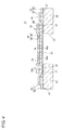
- Fig. 5 is a bottom view of a back plate 14.
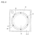
- Fig. 6 is a plan view of a state in which the back plate 14 is removed from the acoustic sensor 31.
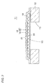
- Fig. 7 is a bottom view of the back plate 14 in which acoustic holes 38 are not shown and only stoppers 42a, 42b are shown.
- the acoustic sensor 31 is a capacitance type element formed using a MEMS technique, where a diaphragm 33 (vibration electrode film) is arranged on an upper surface of a silicon substrate 32 (semiconductor substrate) through an anchor 37, and a back plate 34 is fixed thereon through a microscopic air gap (void), as shown in Fig. 4 .
- a back chamber 35 (hollow portion) passing through from a front surface to a rear surface is opened in the silicon substrate 32 made of monocrystal silicon.
- the back chamber 35 may have an inner peripheral surface serving as a perpendicular surface, or may be incline to a tapered shape.
- a plurality of anchors 37 each for supporting a beam portion 36 of the diaphragm 33 are arranged on the upper surface of silicon substrate 32. Furthermore, as shown in Fig. 6 , a base part 41 is formed on the upper surface of the silicon substrate 32 so as to surround the diaphragm 33. Furthermore, the region on the outer side than the base part 41 of the upper surface of the silicon substrate 32 is covered with an adhesive layer 47 thinner than the base part 41.
- the anchor 37 and the base part 41 are made from SiO 2
- the adhesive layer 47 is made from SiO 2 or polysilicon.
- the diaphragm 33 is formed by a substantially circular plate shaped polysilicon thin film having conductivity.
- a plurality of beam portions 36 are extended from the outer peripheral edge of the diaphragm 33, and the beam portions 36 are arranged at equal interval.
- a band plate shaped extraction wiring 43 is extended toward the outer side from the diaphragm 33.
- the diaphragm 33 is arranged on the upper surface of the silicon substrate 32 so as to cover the upper surface of the back chamber 35, and the lower surface of the beam portion 36 is fixed to the anchor 37. Therefore, the diaphragm 33 is supported in air, and a narrow ventilation hole 57 for passing through the acoustic vibration is formed between the lower surface at the outer peripheral part of the diaphragm 33 and the upper surface of the silicon substrate 32.
- the back plate 34 has a fixed electrode film 40 made of polysilicon arranged on the lower surface of a plate portion 39 (fixed film) made of SiN-
- the back plate 34 is formed to a dome shape and includes a hollow portion thereunder, which hollow portion covers the diaphragm 33.
- the height of the hollow portion under the back plate 34 (height from the upper surface of the silicon substrate 32 to the lower surface of the fixed electrode film 40) is equal to the thickness of the base part 41 formed on the upper surface of the silicon substrate 32 from reasons of manufacturing.
- a microscopic air gap (void) is formed between the lower surface of the back plate 34 (i.e., lower surface of the fixed electrode film 40) and the upper surface of the diaphragm 33.
- the fixed electrode film 40 and the diaphragm 33 face each other and configure a capacitor.
- a great number of acoustic holes (acoustic perforations) 38 for passing the acoustic vibration are perforated so as to pass through from the upper surface to the lower surface over substantially the entire back plate 34.
- the acoustic holes 38 are regularly arrayed.
- the acoustic holes 38 are arrayed to a triangular shape along three directions forming an angle of 120° with respect to each other, but may be formed to a rectangular or a concentric shape.
- two types of microscopic stoppers 42a, 42b having a cylindrical shape are projecting out at the lower surface of the back plate 34.
- the stoppers 42a, 42b are integrally projecting out from the lower surface of the plate portion 39, pass through the fixed electrode film 40, and projected out to the lower surface of the back plate 34.
- the stoppers 42a, 42b are made of SiN same as the plate portion 39, and have insulating property.
- the stopper 42a and the stopper 42b have equal projection length, and the lower end faces of the stoppers 42a, 42b are aligned on the same plane, but the stopper 42a has a diameter greater than the stopper 42b.
- the thin stoppers 42b are arranged at the outer peripheral area of the back plate 34, and the thick stoppers 42a are arranged at the interior area (region on the inner side than the outer peripheral area) of the back plate 34.
- the diaphragm 33 has a larger area than the fixed electrode film 40 in the illustrated example of the first embodiment, and the thin stoppers 42b are arranged in a region that is on the outer side than the fixed electrode film 40 and that faces the diaphragm 33.
- the thick stoppers 42a are arranged in a region where the fixed electrode film 40 is arranged.
- the stoppers 42a and 42b are regularly arranged as a whole, The stoppers 42a, 42b may be arranged at the center of the region surrounded with the acoustic holes 38 or may be arranged at positions proximate to one of the acoustic holes 38.
- a protective film 53 is continuously extended over the entire periphery from the outer peripheral edge of the canopy-shaped plate portion 39.
- the inner peripheral part of the protective film 53 is a base covering part 51 having a reverse groove shaped cross-section, and the outer peripheral part of the protective film 53 is a flat part 52,
- the plate portion 39 is fixed to the upper surface of the silicon substrate 32, the base covering part 51 covers the base part 41, and the flat part 52 covers the upper surface of the adhesive layer 47.
- the extraction wiring 43 is fixed to the base part 41, and the extraction wiring 44 extended from the fixed electrode film 40 is also fixed to the upper surface o the base part 41.
- An opening is formed in the base covering part 51, where a movable side electrode pad 46 is formed on the upper surface of the extraction wiring 43 through the relevant opening and the movable side electrode pad 46 is conducted to the extraction wiring 43 (therefore, to the diaphragm 33).
- the fixed side electrode pad 45 arranged on the upper surface of the plate portion 39 is conducted to the extraction wiring 44 (therefore, to the fixed electrode film 40) through the through hole and the like.
- the diaphragm 33 which is a thin film, vibrates by the acoustic vibration.
- the electrostatic capacitance between the diaphragm 33 and the fixed electrode film 40 changes when the diaphragm 33 vibrates and a gap distance between the diaphragm 33 and the fixed electrode film 40 changes.
- the acoustic vibration (change in sound pressure) sensed by the diaphragm 33 becomes the change in electrostatic capacitance between the diaphragm 33 and the fixed electrode film 40, and is outputted as an electrical signal.
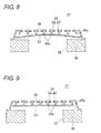
- Such an acoustic sensor 31 has satisfactory impact resistance. Since the diaphragm 33 has the outer peripheral part held by the beam portions 36, the central part of the diaphragm 33 first hits the stopper, as shown in Fig. 8 , when the acoustic sensor 31 drops. In such an acoustic sensor 31, however, the stoppers 42a in the interior area have a large diameter and hence the contacting area when the diaphragm 33 hits the stoppers 42a is large and the impact on the diaphragm 33 is alleviated. Therefore, the diaphragm 33 is less likely to break and the drop resistance of the acoustic sensor 31 increases.
- the diaphragm 33 may hit the stoppers other than when the acoustic sensor 31 is dropped such as when wind pressure is applied from the back chamber 35 to the diaphragm 33, or when acceleration is applied on the acoustic sensor 31. In such cases as well, the impact is alleviated and the diaphragm 33 is less likely to break since the central part of the diaphragm 33 hits the thick stoppers 42a. Therefore, according to the acoustic sensor 31, the impact resistance of the diaphragm 33 can be enhanced without being limited to the drop resistance.
- the sticking resistance property also increases. Even if the entire diaphragm 33 sticks to the lower surface of the stoppers 42a, 42b as shown in Fig. 9 , the elastic restoring force of returning to the original position is strong at the central part of the diaphragm 33 compared to its outer peripheral part and hence the central part of the diaphragm 33 tends to easily strip from the stoppers 42a and return to the original position as shown in Fig. 10 even if the diameter of the stopper 42a is large.
- the outer peripheral part of the diaphragm 33 portion not fixed with the beam portion 36 of the outer peripheral part
- the outer peripheral part of the diaphragm 33 has weak elastic restoring force compared to the central part.
- the contacting area between the outer peripheral part of the diaphragm 33 and the stopper 42b is small since the diameter of the stopper 42b is small, so that the outer peripheral part of the diaphragm 33 easily strips from the stopper 42b and returns to the original position even with a relatively small elastic restoring force and hence sticking is less likely to occur.
- the diameter of the stopper 42a arranged in the interior area of the back plate 34 is increased and the diameter of the stopper 42b arranged in the outer peripheral area is reduced to achieve the contradicting effect of enhancing impact resistance and preventing sticking of the acoustic sensor 31.
- the dimension or the like of the stopper 42a, 42b that can optimize the functional effects of the present invention will now be described.
- the stopper 42a arranged at the central area desirably has a diameter of greater than or equal to 1 ⁇ m to alleviate the impact in time of drop test or the like. If the diameter is smaller than 1 ⁇ m, the contacting area with the diaphragm 33 becomes too small and the alleviation of the impact property in the case where the diaphragm 33 hits becomes insufficient.
- the stopper 42b arranged at the outer peripheral area desirably has a diameter of smaller than or equal to 5 ⁇ m (but smaller than the diameter of the stopper 42a) to prevent sticking of the diaphragm 33. If the diameter is greater than 5 ⁇ m, the contacting area with the diaphragm 33 becomes too large and the holding force at the stopper 42b becomes too large, and the sticking of the diaphragm 33 cannot be reliably prevented,
- the width X of the outer peripheral area is desirably smaller than or equal to 1/4 (i.e., X ⁇ W/4) of the width W of the deforming region of the diaphragm 33. If the width W of the outer peripheral area is greater than 1/4, the area where the stopper 42b of small diameter is arranged becomes wide, and hence the vicinity of the central part of the diaphragm 33 may be in contact with the stopper 42b having a small diameter when impact is applied on the acoustic sensor 31, and the impact resistance may be affected.
- the stoppers 42a, 42b may not sufficiently exhibit the effect in the respective area. Therefore, the ratio of the cross-sectional area of the stopper 42b with respect to the cross-sectional area of the stopper 42a is preferably smaller than or equal to 0.75, so that the resistance impact and the sticking resistance property are easily satisfied.
- the diameter and the arrangement of the stoppers 42a, 42b are determined according to the strength of the diaphragm 33, the spring constant of the diaphragm 33, the distance (gap distance) between the diaphragm 33 and the back plate 34, the applied load, or the like.
- the diaphragm 33 is a substantially square shape in which the length of one side is 720 ⁇ m, where the strength of the diaphragm 33 is weak if the film thickness is smaller than or equal to 1 ⁇ m, and hence the diameter of the stopper 42a in the interior area is preferably greater than or equal to 3 ⁇ m (e.g., diameter of 5 ⁇ m) in view of the impact resistance in the interior area.
- the diameter of the stopper 42b in the outer peripheral area is preferably a diameter of about half of the cross-sectional area of the stopper 42 (e.g., if diameter of the stopper 42a is 5 ⁇ m, the diameter of the stopper 42b is about 3,5 ⁇ m) in view of the sticking resistance property of the diaphragm 33.
- the width X of the outer peripheral area is preferably about 50 ⁇ m.
- Second to sixth embodiments have structures substantially similar to the acoustic sensor 31 of the first embodiment, and thus schematic views in which the detailed structure is not shown so that aspects different from the first embodiment are clearly illustrated are shown.
- the same reference numerals are denoted in the drawings for portions of the same structure as the first embodiment, and the description thereof will not be given.
- Fig. 11 is a schematic cross-sectional view showing an acoustic sensor 61 according to a second embodiment of the present invention.
- the acoustic sensor 31 of the first embodiment two types of stoppers 42a, 42b having different diameters are arranged on the lower surface of the back plate 34. but three or more types of stoppers having different diameters may be arranged.
- a stopper 42e having the smallest diameter is arranged at the outermost peripheral area E
- a stopper 42d having the second smallest diameter is arranged in an outer peripheral area D on the inner side of the outermost peripheral area E
- a stopper 42c having the largest diameter is arranged in an internal area C on the inner side of the outer peripheral area D at the tower surface of the back plate 34.
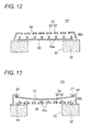
- Fig. 12 is a schematic cross-sectional view showing an acoustic sensor 62 according to a third embodiment of the present invention.
- the stoppers 42a, 42b are arranged on the back plate 34, but the stoppers 42a, 42b are arranged on the upper surface of the diaphragm 33 in the acoustic sensor 62 of the third embodiment.
- the stopper 42b having a small diameter is arranged at the outer peripheral area, and the stopper 42a having a large diameter is arranged in the internal area at the upper surface of the diaphragm 33.
- a hole is formed in the fixed electrode film 40 at the area facing the distal end of the stopper 42a, 42b, so that the upper surface of the diaphragm 33 and the fixed electrode film 40 are prevented from being electrically short circuited.
- the hole may not be formed if a non-conductive material is applied on the surface of the fixed electrode film 40 or the diaphragm 33.
- Fig. 13 is a schematic cross-sectional view showing an acoustic sensor 63 according to a fourth embodiment of the present invention.
- the back plate 34 is arranged on the upper surface of the silicon substrate 32, and the diaphragm 33 is arranged on the back plate 34 facing the back plate 34.
- the back plate 34 has the fixed electrode film 40 formed on the upper surface of the plate portion 39, and is fixed to the upper surface of the silicon substrate 32 by a spacer 55.
- the diaphragm 33 is supported by a supporting portion 54 fixed to the silicon substrate 32.
- the stoppers 42a, 42b are projected out from the upper surface of the back plate 34, where the stopper 42a having a large diameter is arrayed in the internal area of the back plate 34 and the stopper 42b having a small diameter is arrayed in the outer peripheral area.
- Fig. 14 is a schematic cross-sectional view showing an acoustic sensor 64 according to a fifth embodiment of the present invention.
- the configurations of the diaphragm 33 and the back plate 34 are similar to the fourth embodiment.
- This embodiment differs from the fourth embodiment in that the stoppers 42a, 42b are arranged on the lower surface of the diaphragm 33.
- Fig. 15 is a cross-sectional view showing an acoustic sensor 65 according to a sixth embodiment of the present invention.
- projections 56a, 56b are arranged on the lower surface of the diaphragm 33 in the ventilation hole 57.
- the projection 56b arranged in the outer peripheral area has a smaller diameter than the projection 56a arranged in the inner peripheral area.
- the gap distance between the diaphragm 33 and the back plate 34 can be prevented from changing when the edge of the diaphragm 33 sticks to the upper surface of the silicon substrate 32 since the projections 56a, 56b are arranged on the lower surface of the diaphragm 33. Furthermore, the ventilation hole 57 can be prevented from narrowing and the ventilation hole 57 can be prevented from being blocked,
- the inner peripheral area of the diaphragm 33 tends to strongly hit the silicon substrate 32, but the impact of the diaphragm 33 is alleviated since the diameter of the projection 56a of the inner peripheral area is large.
- the projection 56b in the outer peripheral area that is likely to stick to the silicon substrate 32 as a free end has a small diameter, and the contacting area with the silicon substrate 32 is small, so that the sticking of the diaphragm 33 and the silicon substrate 32 can be prevented.
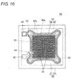
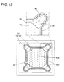
- Fig. 16 its a plan view showing an acoustic sensor 66 according to a seventh embodiment of the present invention.
- Fig. 17 is a plan view showing the fixed electrode film 40 and the diaphragm 33 with the plate portion 39 removed.
- Fig. 18 is a bottom view of the back plate 34 showing the arrangement of the stoppers 42a, 42b in the acoustic sensor 66, where one part is shown in an enlarged manner
- the acoustic sensor 66 has a structure substantially similar to the acoustic sensor 31 of the first embodiment, but the diaphragm 33 and the back plate 34 have a substantially rectangular shape.
- the beam portions 36 are extended in the diagonal direction from the four corners of the substantially rectangular diaphragm 33, and the lower surface of each beam portion 36 is supported by the anchor 37.
- the back plate 34 has the fixed electrode film 40 of octagon shape formed at the lower surface of the substantially rectangular plate portion 39.
- the stopper 42b having a small diameter is projected out in the outer peripheral area of the lower surface of the back plate 34, and the stopper 42a having a large diameter is projected out in the interior area thereof. Therefore, in the acoustic sensor 66 as well, the impact resistance of the diaphragm 33 can be enhanced so that the breakage of the diaphragm 33 can be prevented, and furthermore, the sticking of the diaphragm 33 is less likely to occur.
Landscapes
- Physics & Mathematics (AREA)
- General Physics & Mathematics (AREA)
- Engineering & Computer Science (AREA)
- Acoustics & Sound (AREA)
- Signal Processing (AREA)
- Electrostatic, Electromagnetic, Magneto- Strictive, And Variable-Resistance Transducers (AREA)
- Pressure Sensors (AREA)
- Micromachines (AREA)
Abstract
Description
- The present invention relates to acoustic sensors, and specifically to a MEMS (Micro Electro Mechanical Systems) type acoustic sensor manufactured using a MEMS technique.
- A capacitance type acoustic sensor is disclosed in Japanese Patent No.
4338395 4338395 - In such a capacitance type acoustic sensor, the diaphragm sometimes fixes to the fixed electrode film (hereinafter a state or a phenomenon in which the diaphragm is partially or substantially entirely fixed to the fixed electrode film so that the gap is eliminated is called a stick) in the manufacturing process or during use. When the diaphragm sticks to the fixed electrode film, the acoustic vibration cannot be detected by the acoustic sensor since the vibration of the diaphragm is inhibited.
- The cause of sticking in the acoustic sensor is as follows (details in Japanese Unexamined Patent Publication No.
2008-301430 - The first stage of sticking may also occur, such as the diaphragm may attach to the fixed electrode film when a large sound pressure or drop impact is applied on the diaphragm thereby greatly displacing the diaphragm, or the diaphragm may attach to the fixed electrode film when charged with static electricity.
- An acoustic sensor in which a great number of stoppers (projections) are arranged on a surface facing the diaphragm of the fixed electrode film to prevent the sticking of the diaphragm is known. Such an acoustic sensor is disclosed in Japanese Unexamined Patent Publication No.
2006-157863 -
Fig. 1 andFig .2 is a plan view and a cross-sectional view each showing an acoustic sensor including a stopper. InFig, 1 andFig. 2 , a mode similar to the acoustic sensor of a first embodiment of a conventional example is shown to facilitate the comparison with a first embodiment of the present invention. In anacoustic sensor 11, aback chamber 15 passes through from an upper surface to a lower surface of asilicon substrate 12, and adiaphragm 13 of thin film form made of polysilicon is arranged on the upper surface of thesilicon substrate 12 to cover an upper surface of theback chamber 15. Furthermore, a canopy shapedback plate 14 is fixed to the upper surface of thesilicon substrate 12 so as to cover thediaphragm 13. Theback plate 14 has a fixedelectrode film 20 made of polysilicon arranged on a lower surface of aplate portion 19 made of SiN. A microscopic air gap is formed between thediaphragm 13 and thefixed electrode film 20, where thediaphragm 13 and thefixed electrode film 20 configure a capacitor. A great number ofacoustic holes 18 for passing the acoustic vibration are opened in theentire back plate 14. A plurality ofstoppers 22 each having projection shape of the same length and the same diameter are arranged at substantially equal interval over the entire lower surface of a region facing thediaphragm 13 of theback plate 14. - According to such an
acoustic sensor 11, a distal end face of eachstopper 22 comes into contact with thediaphragm 13 even when thediaphragm 13 is greatly displaced thereby preventing thediaphragm 13 from overly approaching theback plate 14 and inhibiting the sticking of thediaphragm 13. - The holding force between the
diaphragm 13 and theback plate 14 in the second stage of sticking is known to have correlation with a contacting area of thediaphragm 13 and theback plate 14. In other words, the contacting area of thediaphragm 13 and thestopper 22 becomes large and the holding force of thediaphragm 13 becomes large if the diameter of thestopper 22 is large even if thestopper 22 is arranged on theback plate 14. Therefore, sticking easily occurs if the diameter of thestopper 22 is large even if thestopper 22 is arranged on theback plate 14. - Therefore, the
stopper 22 is to be arranged on theback plate 14 and the diameter of thestopper 22 is to be preferably made as small as possible to reduce the contacting area of thediaphragm 13 and theback plate 14 in order to prevent sticking of thediaphragm 13. - however, in the drop accident at the time of actual use or the drop test, the
diaphragm 13 hits thestopper 22 when theacoustic sensor 11 is dropped thereby applying a mechanical load on thediaphragm 13. Therefore, if the diameter of thestopper 22 is narrow, a large mechanical load applies on thediaphragm 13 and thediaphragm 13 may easily break when theacoustic sensor 11 is dropped and thediaphragm 13 hits thestopper 22. - Therefore, in the conventional acoustic sensor, the performance of preventing sticking and the drop resistance property are in contradicting relationship with each other, and an acoustic sensor that satisfies both properties could not be formed. Japanese Unexamined Patent Publication No.
2008-301430 - The present invention has been devised to solve the problems described above, and an object thereof is to provide an acoustic sensor in which sticking of the diaphragm can be prevented and also in which the diaphragm is less likely to break by impact when the sensor is dropped.
- In accordance with one aspect of the present invention, there is provided an acoustic sensor, including a back plate inducing a fixed film arranged on an upper side of a semiconductor substrate and a fixed electrode film arranged on the fixed film, and a vibration electrode film arranged on an upper side of the semiconductor substrate to face the back plate through a void, for converting an acoustic vibration to change in electrostatic capacitance between the vibration electrode film and the fixed electrode film, wherein a plurality of projections are arranged on a surface on the void side of at least one of the back plate and the vibration electrode film, and a cross-sectional area of the projection is differed according to a projection forming region in at least one of the back plate and the vibration electrode film.
- In the acoustic sensor described above, the semiconductor substrate is formed with the hollow portion from the upper surface to the lower side, the vibration electrode film is arranged on the upper surface of the semiconductor substrate, the back plate is fixed on the upper surface of the semiconductor substrate so as to cover the vibration electrode film, and a plurality of acoustic holes are opened in the back plate. Alternatively, the back plate may be fixed on the upper surface of the semiconductor substrate, and the vibration electrode film may be arranged on the upper side of the back plate.
- According to the acoustic sensor of the present invention, a plurality of types of projections having different cross-sectional areas are arranged so that the forming region of the projection having a relatively small cross-sectional area where sticking is less likely to occur and the forming region of the projection having a relatively large cross-sectional area where impact applied on the vibration electrode film can be reduced are differed, so that the sticking of the vibration electrode film can be prevented by optimizing the forming region of the projections having different cross-sectional areas, and the breakage of the vibration electrode film is less likely to occur by the impact when the sensor is dropped.
- In an aspect of the acoustic sensor according to the present invention, three or more types of projections having different cross-sectional areas are arranged, where the projections are arranged so that the cross-sectional area sequentially becomes smaller toward the outer peripheral side from the center of at least one of the back plate and the vibration electrode film. In such an aspect, the cross-sectional area of the projection is small in the outer peripheral area where the elastic restoring force when the vibration electrode film is the free end and sticks to the back plate is weak, so that the holding force in the outer peripheral area when the vibration electrode film sticks can be reduced and the sticking of the vibration electrode film is less likely to occur. Since the cross-sectional area of the projection is large at the central part where the vibration electrode film tends to easily hit the back plate the first when receiving the impact or the like, the impact to be applied on the vibration electrode film can be alleviated. Therefore, according to this aspect, the sticking of the vibration electrode film can be prevented and the breakage of the vibration electrode film due to the impact when the sensor is dropped can be prevented.
- In another aspect of the acoustic sensor according to the present invention, the projection having a relatively small cross-sectional area is arranged in the outer peripheral area of at least one of the back plate and the vibration electrode film, and the projection having a relatively large cross-sectional area is arranged in the internal area of at least one of the back plate and the vibration electrode film. In such an aspect, the cross-sectional area of the projection is small in the outer peripheral area where the elastic restoring force when the vibration electrode film is a free end and sticks to the back plate is weak, so that the holding force in the outer peripheral area when the vibration electrode film sticks can be reduced and sticking is less likely to occur. Furthermore, since the cross-sectional of the projection is large in the internal where the vibration electrode film tends to easily hit the back plate the first when receiving the impact or the like, the impact to be applied on the vibration electrode film can be alleviated. Therefore, according to this aspect, the sticking of the vibration electrode film can be prevented and the breakage of the vibration electrode film due to the impact when the sensor is dropped can be prevented.
- In such an aspect, the width of the outer peripheral area where the projection having a relatively small cross-sectional area is arranged is preferably smaller than or equal to 1/4 of the width of the back plate or the vibration electrode film. If the width of the outer peripheral area is greater 1/4, the vibration electrode film may be in contact with the projection having a small cross-sectional area and break when impact is applied, and hence the impact resistance may be affected.
- In an aspect where the vibration electrode film is arranged on the upper surface of the semiconductor substrate and the back plate is arranged on the upper surface of the semiconductor substrate so as to cover the vibration electrode film, a plurality of projections are arranged in a region facing the upper surface of the semiconductor substrate of the lower surface of the vibration electrode film, and the cross-sectional area of the projection arranged at the outer peripheral part of the region may be smaller than the cross-sectional area of the projection arranged at the inner peripheral part of the region. According to such an aspect, the vibration electrode film can be prevented from sticking to the upper surface of the semiconductor substrate, and the vibration electrode film can be prevented from hitting the semiconductor substrate and breaking due to the impact or the like.
- The means for solving the problems of the invention has a characteristic of appropriately combining the configuring elements described above, and the present invention enables a great number of variations by the combination of the configuring elements.
-
-
Fig. 1 is a plan view of an acoustic sensor of a conventional example; -
Fig. 2 is a cross-sectional view of the acoustic sensor shown inFig. 1 ; -
Fig. 3 is a plan view showing an acoustic sensor of a first embodiment according to the present invention; -
Fig. 4 is a cross-sectional view showing the acoustic sensor of the first embodiment; -
Fig. 5 is a bottom view of a back plate in the acoustic sensor of the first embodiment; -
Fig. 6 is a plan view showing a state in which a back plate is removed from the acoustic sensor of a first embodiment; -
Fig, 7 is a bottom view of the back plate showing an arrangement of stoppers according to the first embodiment; -
Fig. 8 is a schematic cross-sectional view for describing functional effects of the acoustic sensor of the first embodiment; -
Fig. 9 is a schematic cross-sectional view for describing the functional effects of the acoustic sensor of the first embodiment; -
Fig. 10 is a schematic cross-sectional view for describing the functional effects of the acoustic sensor of the first embodiment; -
Fig, 11 is a schematic cross-sectional view showing an acoustic sensor according to a second embodiment of the present invention; -
Fig. 12 is a schematic cross-sectional view showing an acoustic sensor according to a third embodiment of the present invention; -
Fig. 13 is a schematic cross-sectional view showing an acoustic sensor according to a fourth embodiment of the present invention; - Fin. 14 is a schematic cross-sectional view showing an acoustic sensor according to a fifth embodiment of the present invention;
-
Fig. 15 is a cross-sectional view showing an acoustic sensor according to a sixth embodiment of the present invention; - Pig. 16 is a plan view showing an acoustic sensor according to a seventh embodiment of the present invention:
-
Fig. 17 is a plan view showing a state in which a plate portion is removed in the acoustic sensor of the seventh embodiment; and -
Fig. 18 is a bottom view of a back plate showing an arrangement of stoppers in the seventh embodiment. - Hereinafter, preferred embodiments of the present invention will be described with reference to the accompanying drawings. Note that the present invention is not limited to the following embodiments, and various design changes can be made within a scope not deviating from the gist of the present invention.
- The structure of an
acoustic sensor 31 according to a first embodiment of the present invention will be described with reference toFigs. 3 to 7 .Fig. 3 is a plan view showing theacoustic sensor 31 of the first embodiment.Fig. 4 is a cross-sectional view of theacoustic sensor 31.Fig. 5 is a bottom view of aback plate 14.Fig. 6 is a plan view of a state in which theback plate 14 is removed from theacoustic sensor 31.Fig. 7 is a bottom view of theback plate 14 in whichacoustic holes 38 are not shown and onlystoppers - The
acoustic sensor 31 is a capacitance type element formed using a MEMS technique, where a diaphragm 33 (vibration electrode film) is arranged on an upper surface of a silicon substrate 32 (semiconductor substrate) through ananchor 37, and aback plate 34 is fixed thereon through a microscopic air gap (void), as shown inFig. 4 . - A back chamber 35 (hollow portion) passing through from a front surface to a rear surface is opened in the
silicon substrate 32 made of monocrystal silicon. Theback chamber 35 may have an inner peripheral surface serving as a perpendicular surface, or may be incline to a tapered shape. - A plurality of
anchors 37 each for supporting abeam portion 36 of thediaphragm 33 are arranged on the upper surface ofsilicon substrate 32.
Furthermore, as shown inFig. 6 , abase part 41 is formed on the upper surface of thesilicon substrate 32 so as to surround thediaphragm 33. Furthermore, the region on the outer side than thebase part 41 of the upper surface of thesilicon substrate 32 is covered with anadhesive layer 47 thinner than thebase part 41. Theanchor 37 and thebase part 41 are made from SiO2 Theadhesive layer 47 is made from SiO2 or polysilicon. - As shown in
Fig. 6 , thediaphragm 33 is formed by a substantially circular plate shaped polysilicon thin film having conductivity. A plurality ofbeam portions 36 are extended from the outer peripheral edge of thediaphragm 33, and thebeam portions 36 are arranged at equal interval. A band plate shapedextraction wiring 43 is extended toward the outer side from thediaphragm 33. - The
diaphragm 33 is arranged on the upper surface of thesilicon substrate 32 so as to cover the upper surface of theback chamber 35, and the lower surface of thebeam portion 36 is fixed to theanchor 37. Therefore, thediaphragm 33 is supported in air, and anarrow ventilation hole 57 for passing through the acoustic vibration is formed between the lower surface at the outer peripheral part of thediaphragm 33 and the upper surface of thesilicon substrate 32. - The
back plate 34 has a fixedelectrode film 40 made of polysilicon arranged on the lower surface of a plate portion 39 (fixed film) made of SiN- Theback plate 34 is formed to a dome shape and includes a hollow portion thereunder, which hollow portion covers thediaphragm 33. The height of the hollow portion under the back plate 34 (height from the upper surface of thesilicon substrate 32 to the lower surface of the fixed electrode film 40) is equal to the thickness of thebase part 41 formed on the upper surface of thesilicon substrate 32 from reasons of manufacturing. A microscopic air gap (void) is formed between the lower surface of the back plate 34 (i.e., lower surface of the fixed electrode film 40) and the upper surface of thediaphragm 33. The fixedelectrode film 40 and thediaphragm 33 face each other and configure a capacitor. - A great number of acoustic holes (acoustic perforations) 38 for passing the acoustic vibration are perforated so as to pass through from the upper surface to the lower surface over substantially the
entire back plate 34. As shown inFig. 3 andFig. 5 , theacoustic holes 38 are regularly arrayed. In the illustrated example, theacoustic holes 38 are arrayed to a triangular shape along three directions forming an angle of 120° with respect to each other, but may be formed to a rectangular or a concentric shape. - As shown in
Fig. 4 andFig. 5 , two types ofmicroscopic stoppers back plate 34. Thestoppers plate portion 39, pass through the fixedelectrode film 40, and projected out to the lower surface of theback plate 34. Thestoppers plate portion 39, and have insulating property. Thestopper 42a and thestopper 42b have equal projection length, and the lower end faces of thestoppers stopper 42a has a diameter greater than thestopper 42b. - As shown in
Fig. 7 (acoustic holes 38 are not shown), thethin stoppers 42b are arranged at the outer peripheral area of theback plate 34, and thethick stoppers 42a are arranged at the interior area (region on the inner side than the outer peripheral area) of theback plate 34. in particular, thediaphragm 33 has a larger area than the fixedelectrode film 40 in the illustrated example of the first embodiment, and thethin stoppers 42b are arranged in a region that is on the outer side than the fixedelectrode film 40 and that faces thediaphragm 33. Thethick stoppers 42a are arranged in a region where the fixedelectrode film 40 is arranged. - The
stoppers stoppers acoustic holes 38 or may be arranged at positions proximate to one of theacoustic holes 38. - A
protective film 53 is continuously extended over the entire periphery from the outer peripheral edge of the canopy-shapedplate portion 39. The inner peripheral part of theprotective film 53 is abase covering part 51 having a reverse groove shaped cross-section, and the outer peripheral part of theprotective film 53 is aflat part 52, Theplate portion 39 is fixed to the upper surface of thesilicon substrate 32, thebase covering part 51 covers thebase part 41, and theflat part 52 covers the upper surface of theadhesive layer 47. - The
extraction wiring 43 is fixed to thebase part 41, and theextraction wiring 44 extended from the fixedelectrode film 40 is also fixed to the upper surface o thebase part 41. An opening is formed in thebase covering part 51, where a movableside electrode pad 46 is formed on the upper surface of theextraction wiring 43 through the relevant opening and the movableside electrode pad 46 is conducted to the extraction wiring 43 (therefore, to the diaphragm 33). The fixedside electrode pad 45 arranged on the upper surface of theplate portion 39 is conducted to the extraction wiring 44 (therefore, to the fixed electrode film 40) through the through hole and the like. - However, if the acoustic vibration enters the air gap between the
back plate 34 and thediaphragm 33 through theacoustic hole 38 in such anacoustic sensor 31, thediaphragm 33, which is a thin film, vibrates by the acoustic vibration. The electrostatic capacitance between thediaphragm 33 and the fixedelectrode film 40 changes when thediaphragm 33 vibrates and a gap distance between thediaphragm 33 and the fixedelectrode film 40 changes. As a result, in such anacoustic sensor 31, the acoustic vibration (change in sound pressure) sensed by thediaphragm 33 becomes the change in electrostatic capacitance between thediaphragm 33 and the fixedelectrode film 40, and is outputted as an electrical signal. - Such an
acoustic sensor 31 has satisfactory impact resistance. Since thediaphragm 33 has the outer peripheral part held by thebeam portions 36, the central part of thediaphragm 33 first hits the stopper, as shown inFig. 8 , when theacoustic sensor 31 drops. In such anacoustic sensor 31, however, thestoppers 42a in the interior area have a large diameter and hence the contacting area when thediaphragm 33 hits thestoppers 42a is large and the impact on thediaphragm 33 is alleviated. Therefore, thediaphragm 33 is less likely to break and the drop resistance of theacoustic sensor 31 increases. - The
diaphragm 33 may hit the stoppers other than when theacoustic sensor 31 is dropped such as when wind pressure is applied from theback chamber 35 to thediaphragm 33, or when acceleration is applied on theacoustic sensor 31. In such cases as well, the impact is alleviated and thediaphragm 33 is less likely to break since the central part of thediaphragm 33 hits thethick stoppers 42a. Therefore, according to theacoustic sensor 31, the impact resistance of thediaphragm 33 can be enhanced without being limited to the drop resistance. - In the
acoustic sensor 31, the sticking resistance property also increases. Even if theentire diaphragm 33 sticks to the lower surface of thestoppers Fig. 9 , the elastic restoring force of returning to the original position is strong at the central part of thediaphragm 33 compared to its outer peripheral part and hence the central part of thediaphragm 33 tends to easily strip from thestoppers 42a and return to the original position as shown inFig. 10 even if the diameter of thestopper 42a is large. The outer peripheral part of the diaphragm 33 (portion not fixed with thebeam portion 36 of the outer peripheral part) is the free end, and thus the outer peripheral part of thediaphragm 33 has weak elastic restoring force compared to the central part. However, in such anacoustic sensor 31, the contacting area between the outer peripheral part of thediaphragm 33 and thestopper 42b is small since the diameter of thestopper 42b is small, so that the outer peripheral part of thediaphragm 33 easily strips from thestopper 42b and returns to the original position even with a relatively small elastic restoring force and hence sticking is less likely to occur. - According to the
acoustic sensor 31, the diameter of thestopper 42a arranged in the interior area of theback plate 34 is increased and the diameter of thestopper 42b arranged in the outer peripheral area is reduced to achieve the contradicting effect of enhancing impact resistance and preventing sticking of theacoustic sensor 31. - The dimension or the like of the
stopper stopper 42a arranged at the central area desirably has a diameter of greater than or equal to 1 µm to alleviate the impact in time of drop test or the like. If the diameter is smaller than 1 µm, the contacting area with thediaphragm 33 becomes too small and the alleviation of the impact property in the case where thediaphragm 33 hits becomes insufficient. - The
stopper 42b arranged at the outer peripheral area desirably has a diameter of smaller than or equal to 5 µm (but smaller than the diameter of thestopper 42a) to prevent sticking of thediaphragm 33. If the diameter is greater than 5 µm, the contacting area with thediaphragm 33 becomes too large and the holding force at thestopper 42b becomes too large, and the sticking of thediaphragm 33 cannot be reliably prevented, - Assuming the width of the outer peripheral area arranged with the
stopper 42b having a small diameter as shown inFig. 4 is X and the width of the deforming region of thediaphragm 33 is W, the width X of the outer peripheral area is desirably smaller than or equal to 1/4 (i.e., X ≤ W/4) of the width W of the deforming region of thediaphragm 33. If the width W of the outer peripheral area is greater than 1/4, the area where thestopper 42b of small diameter is arranged becomes wide, and hence the vicinity of the central part of thediaphragm 33 may be in contact with thestopper 42b having a small diameter when impact is applied on theacoustic sensor 31, and the impact resistance may be affected. - If the area ratio (ratio of cross-sectional areas perpendicular to the length direction) of the
stopper 42a of the interior area and thestopper 42b of the outer peripheral area is too dose, thestoppers stopper 42b with respect to the cross-sectional area of thestopper 42a is preferably smaller than or equal to 0.75, so that the resistance impact and the sticking resistance property are easily satisfied. - The diameter and the arrangement of the
stoppers diaphragm 33, the spring constant of thediaphragm 33, the distance (gap distance) between thediaphragm 33 and theback plate 34, the applied load, or the like. For instance, thediaphragm 33 is a substantially square shape in which the length of one side is 720 µm, where the strength of thediaphragm 33 is weak if the film thickness is smaller than or equal to 1 µm, and hence the diameter of thestopper 42a in the interior area is preferably greater than or equal to 3 µm (e.g., diameter of 5 µm) in view of the impact resistance in the interior area. Since the restoring force of thediaphragm 33 is small in the outer peripheral area, the diameter of thestopper 42b in the outer peripheral area is preferably a diameter of about half of the cross-sectional area of the stopper 42 (e.g., if diameter of thestopper 42a is 5 µm, the diameter of thestopper 42b is about 3,5 µm) in view of the sticking resistance property of thediaphragm 33. In such a case, the width X of the outer peripheral area is preferably about 50 µm. - Other embodiments will now be described. Second to sixth embodiments have structures substantially similar to the
acoustic sensor 31 of the first embodiment, and thus schematic views in which the detailed structure is not shown so that aspects different from the first embodiment are clearly illustrated are shown. The same reference numerals are denoted in the drawings for portions of the same structure as the first embodiment, and the description thereof will not be given. -
Fig. 11 is a schematic cross-sectional view showing anacoustic sensor 61 according to a second embodiment of the present invention. In theacoustic sensor 31 of the first embodiment, two types ofstoppers back plate 34. but three or more types of stoppers having different diameters may be arranged. - In the
acoustic sensor 61 shown inFig. 11 , astopper 42e having the smallest diameter is arranged at the outermost peripheral area E, astopper 42d having the second smallest diameter is arranged in an outer peripheral area D on the inner side of the outermost peripheral area E, and astopper 42c having the largest diameter is arranged in an internal area C on the inner side of the outer peripheral area D at the tower surface of theback plate 34. -
Fig. 12 is a schematic cross-sectional view showing anacoustic sensor 62 according to a third embodiment of the present invention. In theacoustic sensor 31 of the first embodiment, thestoppers back plate 34, but thestoppers diaphragm 33 in theacoustic sensor 62 of the third embodiment. In theacoustic sensor 62 as well, thestopper 42b having a small diameter is arranged at the outer peripheral area, and thestopper 42a having a large diameter is arranged in the internal area at the upper surface of thediaphragm 33. As a result, the impact resistance of theacoustic sensor 62 can be enhanced, and at the same time, the sticking of thediaphragm 33 can be prevented in the acoustic,sensor 62 as well. InFig. 12 , a hole is formed in the fixedelectrode film 40 at the area facing the distal end of thestopper diaphragm 33 and the fixedelectrode film 40 are prevented from being electrically short circuited. The hole may not be formed if a non-conductive material is applied on the surface of the fixedelectrode film 40 or thediaphragm 33. -
Fig. 13 is a schematic cross-sectional view showing anacoustic sensor 63 according to a fourth embodiment of the present invention. In theacoustic sensor 63, theback plate 34 is arranged on the upper surface of thesilicon substrate 32, and thediaphragm 33 is arranged on theback plate 34 facing theback plate 34. Theback plate 34 has the fixedelectrode film 40 formed on the upper surface of theplate portion 39, and is fixed to the upper surface of thesilicon substrate 32 by aspacer 55. Thediaphragm 33 is supported by a supportingportion 54 fixed to thesilicon substrate 32. Thestoppers back plate 34, where thestopper 42a having a large diameter is arrayed in the internal area of theback plate 34 and thestopper 42b having a small diameter is arrayed in the outer peripheral area. -
Fig. 14 is a schematic cross-sectional view showing anacoustic sensor 64 according to a fifth embodiment of the present invention. In this embodiment, the configurations of thediaphragm 33 and theback plate 34 are similar to the fourth embodiment. This embodiment differs from the fourth embodiment in that thestoppers diaphragm 33. -
Fig. 15 is a cross-sectional view showing anacoustic sensor 65 according to a sixth embodiment of the present invention. In such anacoustic sensor 65,projections diaphragm 33 in theventilation hole 57. Theprojection 56b arranged in the outer peripheral area has a smaller diameter than theprojection 56a arranged in the inner peripheral area. - In this embodiment, the gap distance between the
diaphragm 33 and theback plate 34 can be prevented from changing when the edge of thediaphragm 33 sticks to the upper surface of thesilicon substrate 32 since theprojections diaphragm 33. Furthermore, theventilation hole 57 can be prevented from narrowing and theventilation hole 57 can be prevented from being blocked, - When the acoustic sensor 56 is dropped, the inner peripheral area of the
diaphragm 33 tends to strongly hit thesilicon substrate 32, but the impact of thediaphragm 33 is alleviated since the diameter of theprojection 56a of the inner peripheral area is large. Theprojection 56b in the outer peripheral area that is likely to stick to thesilicon substrate 32 as a free end has a small diameter, and the contacting area with thesilicon substrate 32 is small, so that the sticking of thediaphragm 33 and thesilicon substrate 32 can be prevented. -
Fig. 16 its a plan view showing anacoustic sensor 66 according to a seventh embodiment of the present invention.Fig. 17 is a plan view showing the fixedelectrode film 40 and thediaphragm 33 with theplate portion 39 removed.Fig. 18 is a bottom view of theback plate 34 showing the arrangement of thestoppers acoustic sensor 66, where one part is shown in an enlarged manner - The
acoustic sensor 66 has a structure substantially similar to theacoustic sensor 31 of the first embodiment, but thediaphragm 33 and theback plate 34 have a substantially rectangular shape. Thebeam portions 36 are extended in the diagonal direction from the four corners of the substantiallyrectangular diaphragm 33, and the lower surface of eachbeam portion 36 is supported by theanchor 37. Theback plate 34 has the fixedelectrode film 40 of octagon shape formed at the lower surface of the substantiallyrectangular plate portion 39. - In this
acoustic sensor 66 as well, thestopper 42b having a small diameter is projected out in the outer peripheral area of the lower surface of theback plate 34, and thestopper 42a having a large diameter is projected out in the interior area thereof. Therefore, in theacoustic sensor 66 as well, the impact resistance of thediaphragm 33 can be enhanced so that the breakage of thediaphragm 33 can be prevented, and furthermore, the sticking of thediaphragm 33 is less likely to occur.
Claims (7)
- An acoustic sensor (31, 61, 62, 63, 64, 65, 66), comprising:a back plate (34) including a fixed film arranged on an upper side of a semiconductor substrate and a fixed electrode film (40) arranged on the fixed film; anda vibration electrode film arranged on an upper side of the semiconductor substrate to face the back plate (34) through a void, for converting an acoustic vibration to change in electrostatic capacitance between the vibration electrode film and the fixed electrode film (40), characterized in thata plurality of projections (42a, 42b, 42c, 42d, 42e) are arranged on a surface on the void side of at least one of the back plate (34) and the vibration electrode film, anda cross-sectional area of the projection (42a, 42b, 42c, 42d, 42e) is differed according to a projection forming region in at least one of the back plate (34) and the vibration electrode film,
- The acoustic sensor (31,61, 62, 63, 64, 65, 66) according to claim 1, characterized in that
three or more types of projections (42a, 42b, 42c, 42d, 42e) having different cross-sectional areas are arranged, and
the projections (42a, 42b, 42c, 42d, 42e) are arranged so that the cross-sectional area sequentially becomes smaller toward an outer peripheral side from a center of at least one of the back plate (34) and the vibration electrode film. - The acoustic sensor (31, 61, 62, 63, 64, 65, 66) according to claim 1, characterized in that the projection (42a, 42b, 42c, 42d, 42e) having a relatively small cross-sectional area is arranged in an outer peripheral area of at least one of the back plate (34) and the vibration electrode film, and the projection (42a, 42b, 42c, 42d, 42e) having a relatively large cross-sectional area is arranged in an internal area of at least one of the back plate (34) and the vibration electrode film
- The acoustic sensor (31, 61, 62, 63, 64, 65, 66) according to claim 3, characterized in that a width of the outer peripheral area where the projection (42a, 42b, 42c, 42d, 42e) having a relatively small cross-sectional area is arranged is smaller than or equal to 1/4 of a width of the back plate (34) or the vibration electrode film
- The acoustic sensor (31, 61, 62, 63, 64, 65, 66) according to claim 1, characterized in that the semiconductor substrate is formed with a hollow portion from an upper surface to a lower side, the vibration electrode film is arranged on the upper surface of the semiconductor substrate, the back plate (34) is fixed on the upper surface of the semiconductor substrate so as to cover the vibration electrode film, and a plurality of acoustic holes (38) are opened in the back plate (34).
- The acoustic sensor (31, 61, 62, 63, 64, 65, 66) according to claim 1, characterized in that a plurality of projection (56a, 56b)s are arranged in a region facing an upper surface of the semiconductor substrate of a lower surface of the vibration electrode film, and the cross-sectional area of the projection (56a, 56b) arranged at an outer peripheral part of the region is smaller than the cross-sectional area of the projection (56a, 56b) arranged at an inner peripheral part of the region.
- The acoustic sensor (31, 61, 62, 63, 64, 65, 66) according to claim 1, characterized in that the back plate (34) is fixed on the upper surface of the semiconductor substrate, and the vibration electrode film is arranged on an upper side of the back plate (34).
Applications Claiming Priority (1)
| Application Number | Priority Date | Filing Date | Title |
|---|---|---|---|
| JP2010110946A JP5402823B2 (en) | 2010-05-13 | 2010-05-13 | Acoustic sensor |
Publications (3)
| Publication Number | Publication Date |
|---|---|
| EP2386840A2 true EP2386840A2 (en) | 2011-11-16 |
| EP2386840A3 EP2386840A3 (en) | 2017-03-22 |
| EP2386840B1 EP2386840B1 (en) | 2020-04-01 |
Family
ID=44504361
Family Applications (1)
| Application Number | Title | Priority Date | Filing Date |
|---|---|---|---|
| EP11161591.0A Active EP2386840B1 (en) | 2010-05-13 | 2011-04-08 | Acoustic sensor |
Country Status (5)
| Country | Link |
|---|---|
| US (1) | US8541852B2 (en) |
| EP (1) | EP2386840B1 (en) |
| JP (1) | JP5402823B2 (en) |
| KR (1) | KR101202102B1 (en) |
| CN (1) | CN102325294B (en) |
Cited By (4)
| Publication number | Priority date | Publication date | Assignee | Title |
|---|---|---|---|---|
| EP3334184A1 (en) * | 2016-12-12 | 2018-06-13 | Omron Corporation | Acoustic sensor and capacitive transducer |
| EP3474573A1 (en) * | 2017-10-18 | 2019-04-24 | Omron Corporation | Mems transducer |
| DE102015200490B4 (en) | 2014-03-14 | 2019-07-11 | Omron Corp. | Acoustic transducer |
| US11064299B2 (en) | 2016-07-08 | 2021-07-13 | Omron Corporation | MEMS structure, capacitive sensor, piezoelectric sensor, acoustic sensor having mems structure |
Families Citing this family (35)
| Publication number | Priority date | Publication date | Assignee | Title |
|---|---|---|---|---|
| JP2010271302A (en) * | 2009-04-24 | 2010-12-02 | Seiko Epson Corp | Mems sensor, method of manufacturing mems sensor, and electronic apparatus |
| JP5454345B2 (en) * | 2010-05-11 | 2014-03-26 | オムロン株式会社 | Acoustic sensor and manufacturing method thereof |
| JP5177311B1 (en) * | 2012-02-15 | 2013-04-03 | オムロン株式会社 | Capacitance type sensor and manufacturing method thereof |
| US8987842B2 (en) * | 2012-09-14 | 2015-03-24 | Solid State System Co., Ltd. | Microelectromechanical system (MEMS) device and fabrication method thereof |
| JP5991475B2 (en) * | 2012-09-14 | 2016-09-14 | オムロン株式会社 | Acoustic transducer |
| US9338559B2 (en) * | 2013-04-16 | 2016-05-10 | Invensense, Inc. | Microphone system with a stop member |
| CN103281659B (en) * | 2013-05-03 | 2015-12-23 | 歌尔声学股份有限公司 | MEMS microphone and preparation method thereof |
| JP6288410B2 (en) * | 2013-09-13 | 2018-03-07 | オムロン株式会社 | Capacitive transducer, acoustic sensor and microphone |
| JP6345926B2 (en) * | 2013-10-07 | 2018-06-20 | 新日本無線株式会社 | MEMS device and manufacturing method thereof |
| JP6315429B2 (en) * | 2014-01-24 | 2018-04-25 | 国立大学法人 東京大学 | Sensor |
| US9448126B2 (en) * | 2014-03-06 | 2016-09-20 | Infineon Technologies Ag | Single diaphragm transducer structure |
| JP6311375B2 (en) * | 2014-03-14 | 2018-04-18 | オムロン株式会社 | Capacitive transducer |
| JP6252767B2 (en) * | 2014-03-14 | 2017-12-27 | オムロン株式会社 | Capacitive transducer |
| US10812900B2 (en) | 2014-06-02 | 2020-10-20 | Invensense, Inc. | Smart sensor for always-on operation |
| DE102014212314A1 (en) * | 2014-06-26 | 2015-12-31 | Robert Bosch Gmbh | Micromechanical sensor device |
| KR101610129B1 (en) * | 2014-11-26 | 2016-04-20 | 현대자동차 주식회사 | Microphone and method manufacturing the same |
| KR101619253B1 (en) * | 2014-11-26 | 2016-05-10 | 현대자동차 주식회사 | Microphone and method manufacturing the same |
| US10150664B2 (en) * | 2014-12-15 | 2018-12-11 | Taiwan Semiconductor Manufacturing Co., Ltd. | Microelectromechanical systems (MEMS) stopper structure for stiction improvement |
| TWI549897B (en) * | 2014-12-19 | 2016-09-21 | 立錡科技股份有限公司 | MEMS Chip |
| CN105916084B (en) * | 2015-02-23 | 2019-11-12 | 因文森斯公司 | The intelligence sensor of always-on operation |
| KR102486586B1 (en) * | 2016-06-13 | 2023-01-10 | 주식회사 디비하이텍 | MEMS microphone and method of fabricating the same |
| CN106115607A (en) * | 2016-06-30 | 2016-11-16 | 杭州士兰集成电路有限公司 | MEMS and manufacture method thereof |
| US10281485B2 (en) | 2016-07-29 | 2019-05-07 | Invensense, Inc. | Multi-path signal processing for microelectromechanical systems (MEMS) sensors |
| KR101916052B1 (en) * | 2016-09-09 | 2018-11-07 | 현대자동차 주식회사 | Microphone, manufacturing method and control method therefor |
| CN107857233A (en) * | 2016-09-22 | 2018-03-30 | 中芯国际集成电路制造(上海)有限公司 | A kind of MEMS and preparation method thereof and electronic installation |
| CN108124227B (en) * | 2016-11-29 | 2020-04-28 | 中芯国际集成电路制造(北京)有限公司 | Microphone and method for manufacturing the same |
| CN107105377B (en) * | 2017-05-15 | 2021-01-22 | 潍坊歌尔微电子有限公司 | MEMS microphone |
| CN109704271A (en) * | 2017-10-26 | 2019-05-03 | 中芯国际集成电路制造(上海)有限公司 | A kind of MEMS device and preparation method, electronic device |
| JP7120543B2 (en) * | 2018-08-22 | 2022-08-17 | 日清紡マイクロデバイス株式会社 | Manufacturing method of MEMS element |
| CN110230031B (en) * | 2019-06-28 | 2021-03-02 | 中北大学 | Broadband passive high-temperature-resistant flexible vibration sensor and preparation process thereof |
| JP7522541B2 (en) * | 2019-07-12 | 2024-07-25 | 日清紡マイクロデバイス株式会社 | Piezoelectric element |
| CN110839196B (en) * | 2019-10-28 | 2021-06-08 | 华为终端有限公司 | Electronic equipment and playing control method thereof |
| TWI770543B (en) * | 2020-06-29 | 2022-07-11 | 美律實業股份有限公司 | Microphone structure |
| US11172306B1 (en) * | 2020-08-20 | 2021-11-09 | Shenzhen Ausounds Intelligent Co., Ltd. | Vibration system, panel speaker and active noise reduction wearable electronic device |
| CN111935620B (en) * | 2020-09-23 | 2020-12-25 | 瑶芯微电子科技(上海)有限公司 | MEMS microphone and preparation method thereof |
Citations (3)
| Publication number | Priority date | Publication date | Assignee | Title |
|---|---|---|---|---|
| JP2006157863A (en) | 2004-11-04 | 2006-06-15 | Omron Corp | Capacitive vibration sensor and method for manufacturing same |
| JP2008301430A (en) | 2007-06-04 | 2008-12-11 | Omron Corp | Acoustic sensor |
| JP4338395B2 (en) | 2000-08-11 | 2009-10-07 | ノールズ エレクトロニクス,リミテッド ライアビリティ カンパニー | Small broadband converter |
Family Cites Families (16)
| Publication number | Priority date | Publication date | Assignee | Title |
|---|---|---|---|---|
| JP4045090B2 (en) * | 2001-11-06 | 2008-02-13 | オムロン株式会社 | Adjustment method of electrostatic actuator |
| JP2003163998A (en) * | 2001-11-27 | 2003-06-06 | Seiko Epson Corp | Capacitor microphone, method for manufacturing the same, and electronic equipment |
| JP4036866B2 (en) | 2004-07-30 | 2008-01-23 | 三洋電機株式会社 | Acoustic sensor |
| WO2007015218A2 (en) * | 2005-08-03 | 2007-02-08 | Kolo Technologies, Inc. | Micro-electro-mechanical transducer having an optimized non-flat surface |
| US8126167B2 (en) * | 2006-03-29 | 2012-02-28 | Yamaha Corporation | Condenser microphone |
| CN101123827B (en) * | 2006-08-11 | 2011-11-09 | 中国科学院声学研究所 | Adhesion preventive silicon capacitance sound transmitter chip and its making method |
| JP4144640B2 (en) * | 2006-10-13 | 2008-09-03 | オムロン株式会社 | Method for manufacturing vibration sensor |
| US20080247573A1 (en) * | 2007-04-06 | 2008-10-09 | Novusonic Corporation | Miniature capacitive acoustic sensor with stress-relieved actively clamped diaphragm |
| JP2009028807A (en) * | 2007-07-24 | 2009-02-12 | Rohm Co Ltd | Mems sensor |
| CN101389155A (en) * | 2007-09-12 | 2009-03-18 | 美律实业股份有限公司 | Silicon wafer capacitor microphone |
| JPWO2009101757A1 (en) * | 2008-02-14 | 2011-06-09 | パナソニック株式会社 | Condenser microphone and MEMS device |
| JP2010074523A (en) * | 2008-09-18 | 2010-04-02 | Rohm Co Ltd | Method of etching sacrificial layer, method of manufacturing mems device, and mems device |
| US20100065930A1 (en) * | 2008-09-18 | 2010-03-18 | Rohm Co., Ltd. | Method of etching sacrificial layer, method of manufacturing MEMS device, MEMS device and MEMS sensor |
| JP2010103701A (en) | 2008-10-22 | 2010-05-06 | Rohm Co Ltd | Mems sensor |
| KR101019071B1 (en) | 2009-05-08 | 2011-03-07 | 주식회사 경인전자 | A Capacitive Type MEMS Microphone and Manufacturing Method thereof |
| CN101568057A (en) * | 2009-05-27 | 2009-10-28 | 瑞声声学科技(深圳)有限公司 | Capacitance microphone |
-
2010
- 2010-05-13 JP JP2010110946A patent/JP5402823B2/en not_active Expired - Fee Related
-
2011
- 2011-04-08 EP EP11161591.0A patent/EP2386840B1/en active Active
- 2011-04-14 KR KR1020110034737A patent/KR101202102B1/en active IP Right Grant
- 2011-05-11 CN CN201110120750.9A patent/CN102325294B/en active Active
- 2011-05-12 US US13/106,288 patent/US8541852B2/en active Active
Patent Citations (3)
| Publication number | Priority date | Publication date | Assignee | Title |
|---|---|---|---|---|
| JP4338395B2 (en) | 2000-08-11 | 2009-10-07 | ノールズ エレクトロニクス,リミテッド ライアビリティ カンパニー | Small broadband converter |
| JP2006157863A (en) | 2004-11-04 | 2006-06-15 | Omron Corp | Capacitive vibration sensor and method for manufacturing same |
| JP2008301430A (en) | 2007-06-04 | 2008-12-11 | Omron Corp | Acoustic sensor |
Cited By (7)
| Publication number | Priority date | Publication date | Assignee | Title |
|---|---|---|---|---|
| DE102015200490B4 (en) | 2014-03-14 | 2019-07-11 | Omron Corp. | Acoustic transducer |
| US11064299B2 (en) | 2016-07-08 | 2021-07-13 | Omron Corporation | MEMS structure, capacitive sensor, piezoelectric sensor, acoustic sensor having mems structure |
| DE112017003453B4 (en) | 2016-07-08 | 2021-08-12 | Omron Corporation | MEMS structure, capacitive sensor, piezoelectric sensor, acoustic sensor with MEMS structure |
| EP3334184A1 (en) * | 2016-12-12 | 2018-06-13 | Omron Corporation | Acoustic sensor and capacitive transducer |
| US10555087B2 (en) | 2016-12-12 | 2020-02-04 | Omron Corporation | Acoustic sensor and capacitive transducer |
| EP3474573A1 (en) * | 2017-10-18 | 2019-04-24 | Omron Corporation | Mems transducer |
| US10555089B2 (en) | 2017-10-18 | 2020-02-04 | Omron Corporation | Transducer |
Also Published As
| Publication number | Publication date |
|---|---|
| KR20110125584A (en) | 2011-11-21 |
| EP2386840B1 (en) | 2020-04-01 |
| CN102325294B (en) | 2014-07-09 |
| KR101202102B1 (en) | 2012-11-16 |
| US8541852B2 (en) | 2013-09-24 |
| US20110278684A1 (en) | 2011-11-17 |
| CN102325294A (en) | 2012-01-18 |
| JP5402823B2 (en) | 2014-01-29 |
| JP2011239324A (en) | 2011-11-24 |
| EP2386840A3 (en) | 2017-03-22 |
Similar Documents
| Publication | Publication Date | Title |
|---|---|---|
| EP2386840B1 (en) | Acoustic sensor | |
| EP2387255B1 (en) | Acoustic sensor and microphone | |
| US9544697B2 (en) | Acoustic transducer and microphone | |
| US8379887B2 (en) | Acoustic sensor | |
| JP6252767B2 (en) | Capacitive transducer | |
| US7804969B2 (en) | Silicon microphone with impact proof structure | |
| US8374364B2 (en) | Acoustic sensor and method of manufacturing the same | |
| US9493338B2 (en) | Capacitance type sensor and method of manufacturing the same | |
| US20100176821A1 (en) | Acoustic sensor | |
| EP2386521B1 (en) | Acoustic sensor having protective film and method of manufacturing the same | |
| US9869692B2 (en) | Micromechanical Z-sensor | |
| US20150264476A1 (en) | Acoustic transducer | |
| KR102193337B1 (en) | MEMS structure and capacitive sensor, piezoelectric sensor, acoustic sensor with MEMS structure | |
| JP5267697B2 (en) | Acoustic sensor |
Legal Events
| Date | Code | Title | Description |
|---|---|---|---|
| AK | Designated contracting states |
Kind code of ref document: A2 Designated state(s): AL AT BE BG CH CY CZ DE DK EE ES FI FR GB GR HR HU IE IS IT LI LT LU LV MC MK MT NL NO PL PT RO RS SE SI SK SM TR |
|
| AX | Request for extension of the european patent |
Extension state: BA ME |
|
| PUAI | Public reference made under article 153(3) epc to a published international application that has entered the european phase |
Free format text: ORIGINAL CODE: 0009012 |
|
| PUAL | Search report despatched |
Free format text: ORIGINAL CODE: 0009013 |
|
| AK | Designated contracting states |
Kind code of ref document: A3 Designated state(s): AL AT BE BG CH CY CZ DE DK EE ES FI FR GB GR HR HU IE IS IT LI LT LU LV MC MK MT NL NO PL PT RO RS SE SI SK SM TR |
|
| AX | Request for extension of the european patent |
Extension state: BA ME |
|
| RIC1 | Information provided on ipc code assigned before grant |
Ipc: H04R 19/00 20060101ALI20170210BHEP Ipc: G01H 11/06 20060101AFI20170210BHEP |
|
| STAA | Information on the status of an ep patent application or granted ep patent |
Free format text: STATUS: REQUEST FOR EXAMINATION WAS MADE |
|
| 17P | Request for examination filed |
Effective date: 20170922 |
|
| RBV | Designated contracting states (corrected) |
Designated state(s): AL AT BE BG CH CY CZ DE DK EE ES FI FR GB GR HR HU IE IS IT LI LT LU LV MC MK MT NL NO PL PT RO RS SE SI SK SM TR |
|
| STAA | Information on the status of an ep patent application or granted ep patent |
Free format text: STATUS: EXAMINATION IS IN PROGRESS |
|
| 17Q | First examination report despatched |
Effective date: 20190301 |
|
| GRAP | Despatch of communication of intention to grant a patent |
Free format text: ORIGINAL CODE: EPIDOSNIGR1 |
|
| STAA | Information on the status of an ep patent application or granted ep patent |
Free format text: STATUS: GRANT OF PATENT IS INTENDED |
|
| INTG | Intention to grant announced |
Effective date: 20191022 |
|
| RIN1 | Information on inventor provided before grant (corrected) |
Inventor name: KASAI, TAKASHI |
|
| GRAS | Grant fee paid |
Free format text: ORIGINAL CODE: EPIDOSNIGR3 |
|
| GRAA | (expected) grant |
Free format text: ORIGINAL CODE: 0009210 |
|
| STAA | Information on the status of an ep patent application or granted ep patent |
Free format text: STATUS: THE PATENT HAS BEEN GRANTED |
|
| AK | Designated contracting states |
Kind code of ref document: B1 Designated state(s): AL AT BE BG CH CY CZ DE DK EE ES FI FR GB GR HR HU IE IS IT LI LT LU LV MC MK MT NL NO PL PT RO RS SE SI SK SM TR |
|
| REG | Reference to a national code |
Ref country code: GB Ref legal event code: FG4D |
|
| RIN1 | Information on inventor provided before grant (corrected) |
Inventor name: KASAI, TAKASHI |
|
| REG | Reference to a national code |
Ref country code: CH Ref legal event code: EP Ref country code: AT Ref legal event code: REF Ref document number: 1251967 Country of ref document: AT Kind code of ref document: T Effective date: 20200415 |
|
| REG | Reference to a national code |
Ref country code: DE Ref legal event code: R096 Ref document number: 602011065934 Country of ref document: DE |
|
| REG | Reference to a national code |
Ref country code: IE Ref legal event code: FG4D |
|
| PG25 | Lapsed in a contracting state [announced via postgrant information from national office to epo] |
Ref country code: BG Free format text: LAPSE BECAUSE OF FAILURE TO SUBMIT A TRANSLATION OF THE DESCRIPTION OR TO PAY THE FEE WITHIN THE PRESCRIBED TIME-LIMIT Effective date: 20200701 |
|
| REG | Reference to a national code |
Ref country code: NL Ref legal event code: MP Effective date: 20200401 |
|
| REG | Reference to a national code |
Ref country code: LT Ref legal event code: MG4D |
|
| PG25 | Lapsed in a contracting state [announced via postgrant information from national office to epo] |
Ref country code: CZ Free format text: LAPSE BECAUSE OF FAILURE TO SUBMIT A TRANSLATION OF THE DESCRIPTION OR TO PAY THE FEE WITHIN THE PRESCRIBED TIME-LIMIT Effective date: 20200401 Ref country code: NL Free format text: LAPSE BECAUSE OF FAILURE TO SUBMIT A TRANSLATION OF THE DESCRIPTION OR TO PAY THE FEE WITHIN THE PRESCRIBED TIME-LIMIT Effective date: 20200401 Ref country code: LT Free format text: LAPSE BECAUSE OF FAILURE TO SUBMIT A TRANSLATION OF THE DESCRIPTION OR TO PAY THE FEE WITHIN THE PRESCRIBED TIME-LIMIT Effective date: 20200401 Ref country code: PT Free format text: LAPSE BECAUSE OF FAILURE TO SUBMIT A TRANSLATION OF THE DESCRIPTION OR TO PAY THE FEE WITHIN THE PRESCRIBED TIME-LIMIT Effective date: 20200817 Ref country code: GR Free format text: LAPSE BECAUSE OF FAILURE TO SUBMIT A TRANSLATION OF THE DESCRIPTION OR TO PAY THE FEE WITHIN THE PRESCRIBED TIME-LIMIT Effective date: 20200702 Ref country code: FI Free format text: LAPSE BECAUSE OF FAILURE TO SUBMIT A TRANSLATION OF THE DESCRIPTION OR TO PAY THE FEE WITHIN THE PRESCRIBED TIME-LIMIT Effective date: 20200401 Ref country code: SE Free format text: LAPSE BECAUSE OF FAILURE TO SUBMIT A TRANSLATION OF THE DESCRIPTION OR TO PAY THE FEE WITHIN THE PRESCRIBED TIME-LIMIT Effective date: 20200401 Ref country code: IS Free format text: LAPSE BECAUSE OF FAILURE TO SUBMIT A TRANSLATION OF THE DESCRIPTION OR TO PAY THE FEE WITHIN THE PRESCRIBED TIME-LIMIT Effective date: 20200801 Ref country code: NO Free format text: LAPSE BECAUSE OF FAILURE TO SUBMIT A TRANSLATION OF THE DESCRIPTION OR TO PAY THE FEE WITHIN THE PRESCRIBED TIME-LIMIT Effective date: 20200701 |
|
| REG | Reference to a national code |
Ref country code: AT Ref legal event code: MK05 Ref document number: 1251967 Country of ref document: AT Kind code of ref document: T Effective date: 20200401 |
|
| PG25 | Lapsed in a contracting state [announced via postgrant information from national office to epo] |
Ref country code: HR Free format text: LAPSE BECAUSE OF FAILURE TO SUBMIT A TRANSLATION OF THE DESCRIPTION OR TO PAY THE FEE WITHIN THE PRESCRIBED TIME-LIMIT Effective date: 20200401 Ref country code: RS Free format text: LAPSE BECAUSE OF FAILURE TO SUBMIT A TRANSLATION OF THE DESCRIPTION OR TO PAY THE FEE WITHIN THE PRESCRIBED TIME-LIMIT Effective date: 20200401 Ref country code: LV Free format text: LAPSE BECAUSE OF FAILURE TO SUBMIT A TRANSLATION OF THE DESCRIPTION OR TO PAY THE FEE WITHIN THE PRESCRIBED TIME-LIMIT Effective date: 20200401 |
|
| REG | Reference to a national code |
Ref country code: CH Ref legal event code: PL |
|
| PG25 | Lapsed in a contracting state [announced via postgrant information from national office to epo] |
Ref country code: AL Free format text: LAPSE BECAUSE OF FAILURE TO SUBMIT A TRANSLATION OF THE DESCRIPTION OR TO PAY THE FEE WITHIN THE PRESCRIBED TIME-LIMIT Effective date: 20200401 |
|
| REG | Reference to a national code |
Ref country code: DE Ref legal event code: R097 Ref document number: 602011065934 Country of ref document: DE |
|
| PG25 | Lapsed in a contracting state [announced via postgrant information from national office to epo] |
Ref country code: EE Free format text: LAPSE BECAUSE OF FAILURE TO SUBMIT A TRANSLATION OF THE DESCRIPTION OR TO PAY THE FEE WITHIN THE PRESCRIBED TIME-LIMIT Effective date: 20200401 Ref country code: CH Free format text: LAPSE BECAUSE OF NON-PAYMENT OF DUE FEES Effective date: 20200430 Ref country code: DK Free format text: LAPSE BECAUSE OF FAILURE TO SUBMIT A TRANSLATION OF THE DESCRIPTION OR TO PAY THE FEE WITHIN THE PRESCRIBED TIME-LIMIT Effective date: 20200401 Ref country code: AT Free format text: LAPSE BECAUSE OF FAILURE TO SUBMIT A TRANSLATION OF THE DESCRIPTION OR TO PAY THE FEE WITHIN THE PRESCRIBED TIME-LIMIT Effective date: 20200401 Ref country code: LI Free format text: LAPSE BECAUSE OF NON-PAYMENT OF DUE FEES Effective date: 20200430 Ref country code: SM Free format text: LAPSE BECAUSE OF FAILURE TO SUBMIT A TRANSLATION OF THE DESCRIPTION OR TO PAY THE FEE WITHIN THE PRESCRIBED TIME-LIMIT Effective date: 20200401 Ref country code: ES Free format text: LAPSE BECAUSE OF FAILURE TO SUBMIT A TRANSLATION OF THE DESCRIPTION OR TO PAY THE FEE WITHIN THE PRESCRIBED TIME-LIMIT Effective date: 20200401 Ref country code: RO Free format text: LAPSE BECAUSE OF FAILURE TO SUBMIT A TRANSLATION OF THE DESCRIPTION OR TO PAY THE FEE WITHIN THE PRESCRIBED TIME-LIMIT Effective date: 20200401 Ref country code: LU Free format text: LAPSE BECAUSE OF NON-PAYMENT OF DUE FEES Effective date: 20200408 Ref country code: MC Free format text: LAPSE BECAUSE OF FAILURE TO SUBMIT A TRANSLATION OF THE DESCRIPTION OR TO PAY THE FEE WITHIN THE PRESCRIBED TIME-LIMIT Effective date: 20200401 |
|
| REG | Reference to a national code |
Ref country code: BE Ref legal event code: MM Effective date: 20200430 |
|
| PLBE | No opposition filed within time limit |
Free format text: ORIGINAL CODE: 0009261 |
|
| STAA | Information on the status of an ep patent application or granted ep patent |
Free format text: STATUS: NO OPPOSITION FILED WITHIN TIME LIMIT |
|
| PG25 | Lapsed in a contracting state [announced via postgrant information from national office to epo] |
Ref country code: PL Free format text: LAPSE BECAUSE OF FAILURE TO SUBMIT A TRANSLATION OF THE DESCRIPTION OR TO PAY THE FEE WITHIN THE PRESCRIBED TIME-LIMIT Effective date: 20200401 Ref country code: SK Free format text: LAPSE BECAUSE OF FAILURE TO SUBMIT A TRANSLATION OF THE DESCRIPTION OR TO PAY THE FEE WITHIN THE PRESCRIBED TIME-LIMIT Effective date: 20200401 Ref country code: BE Free format text: LAPSE BECAUSE OF NON-PAYMENT OF DUE FEES Effective date: 20200430 |
|
| 26N | No opposition filed |
Effective date: 20210112 |
|
| PG25 | Lapsed in a contracting state [announced via postgrant information from national office to epo] |
Ref country code: IE Free format text: LAPSE BECAUSE OF NON-PAYMENT OF DUE FEES Effective date: 20200408 |
|
| PG25 | Lapsed in a contracting state [announced via postgrant information from national office to epo] |
Ref country code: SI Free format text: LAPSE BECAUSE OF FAILURE TO SUBMIT A TRANSLATION OF THE DESCRIPTION OR TO PAY THE FEE WITHIN THE PRESCRIBED TIME-LIMIT Effective date: 20200401 |
|
| REG | Reference to a national code |
Ref country code: DE Ref legal event code: R081 Ref document number: 602011065934 Country of ref document: DE Owner name: MMI SEMICONDUCTOR CO., LTD., JP Free format text: FORMER OWNER: OMRON CORPORATION, KYOTO, JP |
|
| PG25 | Lapsed in a contracting state [announced via postgrant information from national office to epo] |
Ref country code: TR Free format text: LAPSE BECAUSE OF FAILURE TO SUBMIT A TRANSLATION OF THE DESCRIPTION OR TO PAY THE FEE WITHIN THE PRESCRIBED TIME-LIMIT Effective date: 20200401 Ref country code: MT Free format text: LAPSE BECAUSE OF FAILURE TO SUBMIT A TRANSLATION OF THE DESCRIPTION OR TO PAY THE FEE WITHIN THE PRESCRIBED TIME-LIMIT Effective date: 20200401 Ref country code: CY Free format text: LAPSE BECAUSE OF FAILURE TO SUBMIT A TRANSLATION OF THE DESCRIPTION OR TO PAY THE FEE WITHIN THE PRESCRIBED TIME-LIMIT Effective date: 20200401 |
|
| PG25 | Lapsed in a contracting state [announced via postgrant information from national office to epo] |
Ref country code: MK Free format text: LAPSE BECAUSE OF FAILURE TO SUBMIT A TRANSLATION OF THE DESCRIPTION OR TO PAY THE FEE WITHIN THE PRESCRIBED TIME-LIMIT Effective date: 20200401 |
|
| PGFP | Annual fee paid to national office [announced via postgrant information from national office to epo] |
Ref country code: GB Payment date: 20240229 Year of fee payment: 14 |
|
| PGFP | Annual fee paid to national office [announced via postgrant information from national office to epo] |
Ref country code: IT Payment date: 20240313 Year of fee payment: 14 Ref country code: FR Payment date: 20240308 Year of fee payment: 14 |
|
| PGFP | Annual fee paid to national office [announced via postgrant information from national office to epo] |
Ref country code: DE Payment date: 20240227 Year of fee payment: 14 |