EP3334021A1 - Gate driver circuit for power converters incorporating normally on transistors and method - Google Patents
Gate driver circuit for power converters incorporating normally on transistors and method Download PDFInfo
- Publication number
- EP3334021A1 EP3334021A1 EP17184982.1A EP17184982A EP3334021A1 EP 3334021 A1 EP3334021 A1 EP 3334021A1 EP 17184982 A EP17184982 A EP 17184982A EP 3334021 A1 EP3334021 A1 EP 3334021A1
- Authority
- EP
- European Patent Office
- Prior art keywords
- voltage
- gate driver
- power converter
- converter
- normally
- Prior art date
- Legal status (The legal status is an assumption and is not a legal conclusion. Google has not performed a legal analysis and makes no representation as to the accuracy of the status listed.)
- Withdrawn
Links
- 238000000034 method Methods 0.000 title claims abstract description 11
- 230000001360 synchronised effect Effects 0.000 claims abstract description 17
- 239000004065 semiconductor Substances 0.000 claims abstract description 8
- 229910044991 metal oxide Inorganic materials 0.000 claims abstract description 5
- 150000004706 metal oxides Chemical class 0.000 claims abstract description 5
- 238000006243 chemical reaction Methods 0.000 claims abstract description 4
- 239000003990 capacitor Substances 0.000 claims description 14
- 230000001268 conjugating effect Effects 0.000 claims description 2
- 230000005669 field effect Effects 0.000 abstract description 5
- HBMJWWWQQXIZIP-UHFFFAOYSA-N silicon carbide Chemical compound [Si+]#[C-] HBMJWWWQQXIZIP-UHFFFAOYSA-N 0.000 description 3
- 229910010271 silicon carbide Inorganic materials 0.000 description 3
- 229910002601 GaN Inorganic materials 0.000 description 2
- XUIMIQQOPSSXEZ-UHFFFAOYSA-N Silicon Chemical compound [Si] XUIMIQQOPSSXEZ-UHFFFAOYSA-N 0.000 description 2
- 230000015556 catabolic process Effects 0.000 description 2
- 238000012986 modification Methods 0.000 description 2
- 230000004048 modification Effects 0.000 description 2
- 229910052710 silicon Inorganic materials 0.000 description 2
- 239000010703 silicon Substances 0.000 description 2
- 239000000243 solution Substances 0.000 description 2
- JMASRVWKEDWRBT-UHFFFAOYSA-N Gallium nitride Chemical compound [Ga]#N JMASRVWKEDWRBT-UHFFFAOYSA-N 0.000 description 1
- 238000003491 array Methods 0.000 description 1
- 238000004519 manufacturing process Methods 0.000 description 1
- 230000003071 parasitic effect Effects 0.000 description 1
- 230000001105 regulatory effect Effects 0.000 description 1
- 239000012086 standard solution Substances 0.000 description 1
- 230000001052 transient effect Effects 0.000 description 1
- 238000010200 validation analysis Methods 0.000 description 1
Images



Classifications
-
- H—ELECTRICITY
- H02—GENERATION; CONVERSION OR DISTRIBUTION OF ELECTRIC POWER
- H02M—APPARATUS FOR CONVERSION BETWEEN AC AND AC, BETWEEN AC AND DC, OR BETWEEN DC AND DC, AND FOR USE WITH MAINS OR SIMILAR POWER SUPPLY SYSTEMS; CONVERSION OF DC OR AC INPUT POWER INTO SURGE OUTPUT POWER; CONTROL OR REGULATION THEREOF
- H02M1/00—Details of apparatus for conversion
- H02M1/08—Circuits specially adapted for the generation of control voltages for semiconductor devices incorporated in static converters
-
- H—ELECTRICITY
- H02—GENERATION; CONVERSION OR DISTRIBUTION OF ELECTRIC POWER
- H02M—APPARATUS FOR CONVERSION BETWEEN AC AND AC, BETWEEN AC AND DC, OR BETWEEN DC AND DC, AND FOR USE WITH MAINS OR SIMILAR POWER SUPPLY SYSTEMS; CONVERSION OF DC OR AC INPUT POWER INTO SURGE OUTPUT POWER; CONTROL OR REGULATION THEREOF
- H02M3/00—Conversion of DC power input into DC power output
- H02M3/02—Conversion of DC power input into DC power output without intermediate conversion into AC
- H02M3/04—Conversion of DC power input into DC power output without intermediate conversion into AC by static converters
- H02M3/10—Conversion of DC power input into DC power output without intermediate conversion into AC by static converters using discharge tubes with control electrode or semiconductor devices with control electrode
- H02M3/145—Conversion of DC power input into DC power output without intermediate conversion into AC by static converters using discharge tubes with control electrode or semiconductor devices with control electrode using devices of a triode or transistor type requiring continuous application of a control signal
- H02M3/155—Conversion of DC power input into DC power output without intermediate conversion into AC by static converters using discharge tubes with control electrode or semiconductor devices with control electrode using devices of a triode or transistor type requiring continuous application of a control signal using semiconductor devices only
-
- H—ELECTRICITY
- H03—ELECTRONIC CIRCUITRY
- H03K—PULSE TECHNIQUE
- H03K17/00—Electronic switching or gating, i.e. not by contact-making and –breaking
- H03K17/04—Modifications for accelerating switching
- H03K17/042—Modifications for accelerating switching by feedback from the output circuit to the control circuit
- H03K17/04206—Modifications for accelerating switching by feedback from the output circuit to the control circuit in field-effect transistor switches
-
- H—ELECTRICITY
- H02—GENERATION; CONVERSION OR DISTRIBUTION OF ELECTRIC POWER
- H02M—APPARATUS FOR CONVERSION BETWEEN AC AND AC, BETWEEN AC AND DC, OR BETWEEN DC AND DC, AND FOR USE WITH MAINS OR SIMILAR POWER SUPPLY SYSTEMS; CONVERSION OF DC OR AC INPUT POWER INTO SURGE OUTPUT POWER; CONTROL OR REGULATION THEREOF
- H02M1/00—Details of apparatus for conversion
- H02M1/0048—Circuits or arrangements for reducing losses
-
- H—ELECTRICITY
- H03—ELECTRONIC CIRCUITRY
- H03K—PULSE TECHNIQUE
- H03K17/00—Electronic switching or gating, i.e. not by contact-making and –breaking
- H03K17/06—Modifications for ensuring a fully conducting state
- H03K2017/066—Maximizing the OFF-resistance instead of minimizing the ON-resistance
-
- H—ELECTRICITY
- H03—ELECTRONIC CIRCUITRY
- H03K—PULSE TECHNIQUE
- H03K17/00—Electronic switching or gating, i.e. not by contact-making and –breaking
- H03K17/51—Electronic switching or gating, i.e. not by contact-making and –breaking characterised by the components used
- H03K17/56—Electronic switching or gating, i.e. not by contact-making and –breaking characterised by the components used by the use, as active elements, of semiconductor devices
- H03K17/687—Electronic switching or gating, i.e. not by contact-making and –breaking characterised by the components used by the use, as active elements, of semiconductor devices the devices being field-effect transistors
- H03K2017/6875—Electronic switching or gating, i.e. not by contact-making and –breaking characterised by the components used by the use, as active elements, of semiconductor devices the devices being field-effect transistors using self-conductive, depletion FETs
-
- H—ELECTRICITY
- H03—ELECTRONIC CIRCUITRY
- H03K—PULSE TECHNIQUE
- H03K2217/00—Indexing scheme related to electronic switching or gating, i.e. not by contact-making or -breaking covered by H03K17/00
- H03K2217/0081—Power supply means, e.g. to the switch driver
-
- Y—GENERAL TAGGING OF NEW TECHNOLOGICAL DEVELOPMENTS; GENERAL TAGGING OF CROSS-SECTIONAL TECHNOLOGIES SPANNING OVER SEVERAL SECTIONS OF THE IPC; TECHNICAL SUBJECTS COVERED BY FORMER USPC CROSS-REFERENCE ART COLLECTIONS [XRACs] AND DIGESTS
- Y02—TECHNOLOGIES OR APPLICATIONS FOR MITIGATION OR ADAPTATION AGAINST CLIMATE CHANGE
- Y02B—CLIMATE CHANGE MITIGATION TECHNOLOGIES RELATED TO BUILDINGS, e.g. HOUSING, HOUSE APPLIANCES OR RELATED END-USER APPLICATIONS
- Y02B70/00—Technologies for an efficient end-user side electric power management and consumption
- Y02B70/10—Technologies improving the efficiency by using switched-mode power supplies [SMPS], i.e. efficient power electronics conversion e.g. power factor correction or reduction of losses in power supplies or efficient standby modes
Definitions
- the present invention is related to the field of electronics.
- the invention is in relation to a gate driving system that can generate programmable bipolar voltage, in order to drive normally on metal oxide based semiconductor field effect transistors.
- the present invention is capable of driving both the top and the bottom switches of a synchronous buck converter by using bootstrap technique.
- the proposed system uses available positive power supply and employs standard off the shelf drivers that produce unipolar positive voltage.
- Point of Load converter is a DC/DC switched mode power supply that supplies special integrated circuits (IC) such as micro-controllers, field-programmable gate arrays (FPGA) and the like, meeting high peak current demands with low noise margins.
- Synchronous buck converters are widely used as point of load converters for conversion of high DC voltage to low DC voltage with a function rating ranging from about 15V to about 3.3V, at around 6W.
- a conventional buck converter utilizes enhancement mode transistors for example Silicon based power metal oxide semiconductor field effect transistor (MOSFET) for point of load converters.
- MOSFET Silicon based power metal oxide semiconductor field effect transistor
- JFET Silicon Carbide based Junction field effect transistors
- HEMT Gallium Nitride(GaN) based high electron mobility transistors
- SMPS switched mode power supply
- SPGD self-powered gate driver
- SMPS switched mode power supply
- the details provided in the disclosure describes a circuit that translates a unipolar positive gate driver output to a unipolar negative voltage pulse to drive a normally on GaN transistor.
- the driver applies zero voltage when the switch is in on.
- a positive gate source voltage is necessary to ensure low drain source voltage drop across the transistor to minimize the on state conduction losses.
- gate driver circuits capable of providing bipolar voltage from a positive power supply without using SMPS; wherein existing gate drivers for normally off devices can be reused for normally on devices and also wherein the gate driver system that can utilize cost effective fabrications, for a synchronous buck converter with normally on semiconductor devices.
- the present invention discloses a gate driver system for normally on semiconductor switches with standard gate drivers for normally off devices and passive elements capable of providing programmable bipolar gate driving signals from unipolar positive power supply, without making use of extra components such as switched mode power supply, thus offering a cost effective system with improved efficiency.
- the proposed system also employs a boot strapping technique obviating any need of an isolated SMPS to drive the top switch in a synchronous buck converter.
- the present invention is in relation to a synchronous buck converter comprising gate driver system with passive elements incorporated in the circuit to translate unipolar voltage produced by the standard gate driver to a programmable bipolar voltage along with bootstrap technique to drive the pair of, normally on MOSFETs in the synchronous buck converter.
- the present invention is in relation to a power converter comprising-
- the converter is a synchronous buck converter.
- the converter drives a normally on metal oxide semiconductor switch.
- the gate driver of the system is a voltage level shifter and current booster circuit.
- the passive elements comprises
- the bootstrap device is used to drive the top driver (M1).
- the bootstrap device is a capacitor.
- the capacitor is charged from the power source through a diode and resistor when the bottom driver (M2) is on.
- the present invention is also in relation to a method for conversion of unipolar voltage to a bipolar voltage, said method comprising, conjugating power converter of present invention in voltage translator circuit.
- the present invention discloses a synchronous buck converter comprising a gate driver system to control the switches of the power converter.
- the invention describes a circuit with passive elements for converting a unipolar voltage produced by the gate driver to a programmable bipolar voltage, necessary to drive the normally on switches. Also a bootstrap technique is used to drive the top MOSFET that does not require any additional isolated switched mode power supply.
- the present design of the invention bypasses the use of an additional switch mode power supply for obtaining bipolar voltage to drive normally on MOSFETs.
- Figure 1 describes the proposed gate driver system (GDS) along with the power circuit of a synchronous buck converter (SB) supplying a microcontroller IC as a load.
- the entire system as shown in Figure 1 is called a point of load converter.
- the first transistor (MOSFET (M 1 )) and second transistor (MOSFET (M 2 )) are normally on devices.
- V DC is the input voltage
- V o is the regulated output voltage.
- GDS is the gate drive system of the synchronous buck converter (SB) which accepts the signal from PWM 1 and PWM 2 as digital signals and is powered by two positive voltage sources V CCi and V CC .
- the GDS employs a standard gate driver (GD) as shown in the Figure 1 .
- the gate driver (GD) is essentially a voltage level shifter and a current booster circuit.
- a pulse with an amplitude of V CCi with respect to the ground (GND), applied at the input PWM 2 of GD, is translated to a pulse of an amplitude Vcc with respect to the same ground (V EE2 is connected to the ground) at the output pin OP 2 to drive the bottom device M 2 .
- V EE2 is connected to the ground
- a pulse at the input PWM 1 is translated to a pulse of an amplitude (V CC1 - V EE1 ) with respect to the pin V EE1 at the output pin OP 1 of GD.
- the bottom driver uses the positive power source Vcc connected at terminal V CC2 .
- This power supply is referenced to the system ground connected at terminal V EE2 .
- V CC1 referenced at the terminal V EE1 , which is floating and cannot be connected to the system ground.
- a bootstrap capacitor C B is used to provide the supply for the top driver. This capacitor is charged through the diode D B and resistance R B from the source Vcc when the said second transistor (MOSFET M 2 ) is on.
- the charging path of the boot strap capacitor C B shown as red in Figure 1 .
- the resistance R B is used to limit the charging current and the diode D B ensures uni-directional charging. This explains boot strapping. This solution does not require an isolated power supply to drive the top switch.
- Output of GD is unipolar.
- the high level is V CC and the low level is ground or zero.
- this signal needs to be translated to a bipolar signal, with levels V P and -V N respectively with respect to the ground or the V EE2 .
- This bi-polar voltage levels V P and V N can be designed based on the MOSFET characteristics.
- the positive voltage level V P relates to the on state voltage drop of the device which results in conduction loss.
- the negative voltage level V N must ensure proper turn off of the transistor.
- the circuit with resistance (R 1,2 ), capacitance (C 1,2 ) and Zener (Z P1,2 and Z N1,2 ) is used to change the unipolar voltage to a bipolar voltage.
- This voltage translator circuit is identical for both the top and the bottom switches and shown in Figure 2 .
- Zeners Z P and Z N are used to control the positive (V P ) and the negative (-V N ) voltage across gate source terminals of the MOSFET.
- the Zener also protects the gate source terminal from transient over voltages.
- Capacitance C is used to provide the negative voltage required to discharge the internal input capacitance (C iss ) of the MOSFET.
- Resistance Ris used to limit the peak gate current and to control rise and fall time of the gate source voltage or in the other words the switching speed of the MOSFET. During the turn on and turn off transients, the power dissipation occurs in the proposed voltage translator circuit.
- the Zener Z 1 When the transistor is off, the Zener Z 1 is in the break down mode, applying a negative voltage of -V N across the gate source terminals of the MOSFET.
- the gate driver output voltage is zero and the capacitor C is charged to V N .
- a positive voltage of V CC is applied across the gate driver output. This results in charging C and the voltage across the gate source terminal of the MOSFET also rises eventually.
- the Zener Z P breaks down and clamps the gate source voltage at V P .
- the capacitance of C must be close to C iss /( ⁇ -1). This also ensures minimum loss in the gate resistance R.
- the gate resistance can be designed to minimize the switching time. After the gate voltage is clamped to V P , the voltage across the capacitor asymptotically rises to (V CC -V P ). To turn off the switch, a zero voltage is applied at the driver output causing the capacitor to discharge and the gate source voltage to fall. Once the gate source voltage falls below -V N , the Zener Z N breaks down and continues to clamp the gate source voltage to the same level. The capacitor C asymptotically discharges to a voltage of V N .
- the efficiency and power density of the present gate driver circuit is compared with a standard gate driver circuit which uses a bipolar gate driver ( Figure 3 ), capable of applying V P and -V N to charge and discharge the internal capacitance, C iss , of the MOSFET.
- the bipolar gate driver needs to be supplied with an additional switched mode power supply (SMPS) to generate bipolar voltage from unipolar supply.
- SMPS switched mode power supply
- P SMPS accounts for the additional loss in the SMPS. Both K and ⁇ can be chosen close to unity. This shows that the present invention incurs similar loss when compared with a standard gate driver circuit involving additional SMPS and bipolar gate driver. In these circuits, the power loss is independent of the resistance R. If a bootstrap circuit is used in the standard gate driver circuit, it will incur similar loss when compared with the present invention.
- the standard gate driver circuit and present invention uses a resistance (R) to charge or discharge C iss .
- the present invention has additional pair of Zeners (Z P,N ) and capacitor (C).
- the standard gate driver circuit requires an additional SMPS and associated components. Additional bootstrapping may also will be required to provide bipolar voltage in the standard solution leading to lower power density. Hence, comparatively, the proposed solution will achieve better power density.
- the present invention is cost effective as it does not require an SMPS and bipolar gate driver. Off the shelf, unipolar gate driver, widely used for POLs with normally off MOSFETs can also be used in the present invention for generating unipolar voltage.
- FIG 4 shows a working example of the invention.
- the proposed gate driver system (GDS as in Figure 1 ) is implemented with a commercially available gate driver (GD as in Figure 1 ) AD ⁇ M7234, capable of driving normally off devices with unipolar positive voltage pulses.
- the GDS drives the two normally on transistors IXTA6N50D2 (M 1 , M 2 as in Figure 1 ) of a Synchronous buck converter (SB as in Figure 1 ).
- the boot strap circuit parameters are as follows: 1) Boot strap capacitance (C B as in Figure 1 ) 0.22 micro F 2) Boot strap Resistance (R B as in Figure 1 ) 1.3 ⁇ 3) Boot strap diode (D B as in Figure 1 ).
- the operating conditions are as follows: Input Voltage: 15V, Output voltage: 3V, Output power: 6W, Switching frequency, f: 250 kHz,
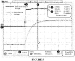
- Figure 5 shows an oscilloscope capture of the output signal of the GD the voltage across the terminals OP 2 and V EE2 (as shown in Figure 1 ) the unipolar pulse in colour code red. This is a pulse of levels zero and 15 V.
- the positive input voltage 15V provides the supply to the GDS system and in particular to GD.
- the proposed voltage translator circuit converts this unipolar pulse to a bipolar one with levels -6V and 2V and applies it to the gate source terminals of normally on transistor M 2 .
- This waveform is also shown in Figure 5 , with colour code green. This confirms the operation of the voltage translator circuit.
- Figure 6 shows the typical voltage and current wave forms of a synchronous buck (SB) converter.
- SB synchronous buck
- the green is the pole voltage waveform (that is the voltage across the bottom transistor M 2 ) with levels 15V and zero. This confirms the proper switching of both the top and the bottom devices of the SB confirming boot strap operation.
- the red signal is the filter inductor current and finally blue is the desired output or load voltage of 3V.
- the present invention is in relation to a synchronous buck converter comprising gate driver system with passive elements for converting unipolar voltage to bipolar voltage along with bootstrap technique to drive pair of normally on MOSFETs in a synchronous buck converter.
Landscapes
- Engineering & Computer Science (AREA)
- Power Engineering (AREA)
- Power Conversion In General (AREA)
- Dc-Dc Converters (AREA)
Abstract
The present invention is in relation to a synchronous buck converter comprising gate driver circuit, incorporated with passive elements for conversion of unipolar voltage produced by a standard gate driver to a bipolar voltage along with bootstrap technique to drive the normally on metal oxide semiconductor field effect transistor.
Description
- The present invention is related to the field of electronics. In particular, the invention is in relation to a gate driving system that can generate programmable bipolar voltage, in order to drive normally on metal oxide based semiconductor field effect transistors. The present invention is capable of driving both the top and the bottom switches of a synchronous buck converter by using bootstrap technique. The proposed system uses available positive power supply and employs standard off the shelf drivers that produce unipolar positive voltage.
- Point of Load converter is a DC/DC switched mode power supply that supplies special integrated circuits (IC) such as micro-controllers, field-programmable gate arrays (FPGA) and the like, meeting high peak current demands with low noise margins. Synchronous buck converters are widely used as point of load converters for conversion of high DC voltage to low DC voltage with a function rating ranging from about 15V to about 3.3V, at around 6W. A conventional buck converter utilizes enhancement mode transistors for example Silicon based power metal oxide semiconductor field effect transistor (MOSFET) for point of load converters. Similarly, wide band gap devices such as Silicon Carbide based Junction field effect transistors (JFET) and Gallium Nitride(GaN) based high electron mobility transistors (HEMT) have been identified as promising power semiconductor devices due to their excellent switching characteristic along with very low on state voltage drop.
- In comparison with Silicon based MOSFET's which are normally off devices, the normally on devices need a negative voltage to turn the switches off. If the control circuit has only positive power supply, a switched mode power supply (SMPS) is required to provide the negative voltage leading to reduction in efficiency of the system, with increase in size and cost.
- In "Self powered gate driver for normally on silicon carbide junction field effect transistors without external power supply"; IEEE Transactions on Power Electronics, Volume: 28, Issue: 3, March 2013, a self-powered gate driver for normally ON silicon carbide JFETs is presented.
- The details provided in the document describes a self-powered gate driver (SPGD)that derives power from the input dc voltage of the converter. As the available dc voltage is positive and unipolar, the SPGD employs a switched mode power supply (SMPS) to provide the negative voltage leading to reduction in efficiency and increase in size and cost.
- Another disclosure titled "Experimental Validation of Normally-On GaN HEMT and Its Gate Drive Circuit in IEEE Transactions on Industry Applications, Volume: 51, Issue: 3, May-June 2015.
- The details provided in the disclosure describes a circuit that translates a unipolar positive gate driver output to a unipolar negative voltage pulse to drive a normally on GaN transistor. The driver applies zero voltage when the switch is in on. A positive gate source voltage is necessary to ensure low drain source voltage drop across the transistor to minimize the on state conduction losses.
- Thus, there is a need for gate driver circuits capable of providing bipolar voltage from a positive power supply without using SMPS; wherein existing gate drivers for normally off devices can be reused for normally on devices and also wherein the gate driver system that can utilize cost effective fabrications, for a synchronous buck converter with normally on semiconductor devices.
- The present invention discloses a gate driver system for normally on semiconductor switches with standard gate drivers for normally off devices and passive elements capable of providing programmable bipolar gate driving signals from unipolar positive power supply, without making use of extra components such as switched mode power supply, thus offering a cost effective system with improved efficiency. The proposed system also employs a boot strapping technique obviating any need of an isolated SMPS to drive the top switch in a synchronous buck converter.
- Accordingly, the present invention is in relation to a synchronous buck converter comprising gate driver system with passive elements incorporated in the circuit to translate unipolar voltage produced by the standard gate driver to a programmable bipolar voltage along with bootstrap technique to drive the pair of, normally on MOSFETs in the synchronous buck converter.
- The features of the present invention can be understood in detail with the aid of appended figures. It is to be noted however, that the appended figures illustrate only typical embodiments of this invention and are therefore not to be considered limiting of its scope for the invention.
-
Figure 1 provides the schematic of the proposed gate driver system (GDS) incorporating a unipolar positive gate driver (GD), proposed voltage translator circuit along with boot strapping, supplied by a positive voltage. It also shows the target application of a PoL converter implemented with a synchronous buck converter which comprises of two normally on devices. -
Figure 2 provides the schematic of the proposed voltage translator circuit. -
Figure 3 provides the traditional gate driving circuit of a normally on device, driven by a bi-polar gate driver. -
Figure 4 provides the photograph of the working example of the present invention. -
Figure 5 and6 provides oscilloscope captures of various different electrical signals described in details in the working example section confirming the operation of the proposed invention. - The foregoing description of the embodiments of the invention has been presented for the purpose of illustration. It is not intended to be exhaustive or to limit the invention to the precise form disclosed as many modifications and variations are possible in light of this disclosure for a person skilled in the art in view of the Figures, description and claims. It may further be noted that as used herein and in the appended claims, the singular "a" "an" and "the" include plural reference unless the context clearly dictates otherwise. Unless defined otherwise, all technical and scientific terms used herein have the same meanings as commonly understood by person skilled in the art.
- The present invention is in relation to a power converter comprising-
- a) a gate driver system with passive elements in circuit; and
- b) configured with a bootstrap device;
- In an embodiment of the present invention, the converter is a synchronous buck converter.
- In another embodiment of the present invention, the converter drives a normally on metal oxide semiconductor switch.
- In still another embodiment of the present invention, the gate driver of the system is a voltage level shifter and current booster circuit.
- In yet another embodiment of the present invention, the passive elements comprises
- a)Zener to control the voltage across the top driver (M1) and bottom driver (M2) of the gate driver system;
- b) Resistor to limit the switching speed of the transistor; and
- c) Capacitor to provide the negative voltage required to discharge the internal input capacitance of the transistors.
- In yet another embodiment of the present invention, the bootstrap device is used to drive the top driver (M1).
- In yet another embodiment of the present invention, the bootstrap device is a capacitor.
- In yet another embodiment of the present invention, the capacitor is charged from the power source through a diode and resistor when the bottom driver (M2) is on.
- The present invention is also in relation to a method for conversion of unipolar voltage to a bipolar voltage, said method comprising, conjugating power converter of present invention in voltage translator circuit.
- The present invention discloses a synchronous buck converter comprising a gate driver system to control the switches of the power converter. The invention describes a circuit with passive elements for converting a unipolar voltage produced by the gate driver to a programmable bipolar voltage, necessary to drive the normally on switches. Also a bootstrap technique is used to drive the top MOSFET that does not require any additional isolated switched mode power supply. The present design of the invention bypasses the use of an additional switch mode power supply for obtaining bipolar voltage to drive normally on MOSFETs.
-
Figure 1 describes the proposed gate driver system (GDS) along with the power circuit of a synchronous buck converter (SB) supplying a microcontroller IC as a load. The entire system as shown inFigure 1 is called a point of load converter. InFigure 1 , the first transistor (MOSFET (M1)) and second transistor (MOSFET (M2)) are normally on devices. VDC is the input voltage and Vo is the regulated output voltage. GDS is the gate drive system of the synchronous buck converter (SB) which accepts the signal from PWM1 and PWM2 as digital signals and is powered by two positive voltage sources VCCi and VCC. - The GDS employs a standard gate driver (GD) as shown in the
Figure 1 . The gate driver (GD) is essentially a voltage level shifter and a current booster circuit. A pulse with an amplitude of VCCi with respect to the ground (GND), applied at the input PWM2 of GD, is translated to a pulse of an amplitude Vcc with respect to the same ground (VEE2 is connected to the ground) at the output pin OP2 to drive the bottom device M2. Similarly, for the said first transistor (M1) a pulse at the input PWM1 is translated to a pulse of an amplitude (VCC1 - VEE1) with respect to the pin VEE1 at the output pin OP1 of GD. - The bottom driver uses the positive power source Vcc connected at terminal VCC2. This power supply is referenced to the system ground connected at terminal VEE2. Similarly we need another power supply at VCC1 referenced at the terminal VEE1, which is floating and cannot be connected to the system ground. So there is a need for an isolated power supply to drive the top MOSFET M1. A bootstrap capacitor CB is used to provide the supply for the top driver. This capacitor is charged through the diode DB and resistance RB from the source Vcc when the said second transistor (MOSFET M2) is on. The charging path of the boot strap capacitor CB shown as red in
Figure 1 . The resistance RB is used to limit the charging current and the diode DB ensures uni-directional charging. This explains boot strapping. This solution does not require an isolated power supply to drive the top switch. - Output of GD, is unipolar. For example, at the output pin OP2, the high level is VCC and the low level is ground or zero. To drive a normally on MOSFET this signal needs to be translated to a bipolar signal, with levels VP and -VN respectively with respect to the ground or the VEE2. This bi-polar voltage levels VP and VN can be designed based on the MOSFET characteristics. The positive voltage level VP relates to the on state voltage drop of the device which results in conduction loss. The negative voltage level VN must ensure proper turn off of the transistor. The circuit with resistance (R1,2), capacitance (C1,2) and Zener (ZP1,2 and ZN1,2) is used to change the unipolar voltage to a bipolar voltage. This voltage translator circuit is identical for both the top and the bottom switches and shown in
Figure 2 . - Zeners ZP and ZN are used to control the positive (VP) and the negative (-VN) voltage across gate source terminals of the MOSFET. The Zener also protects the gate source terminal from transient over voltages. Capacitance C is used to provide the negative voltage required to discharge the internal input capacitance (Ciss) of the MOSFET. Resistance Ris used to limit the peak gate current and to control rise and fall time of the gate source voltage or in the other words the switching speed of the MOSFET. During the turn on and turn off transients, the power dissipation occurs in the proposed voltage translator circuit.
- The operation of the voltage translator circuit for the MOSFET, consisting of the resistance (R), capacitance (C) and Zener (ZP and ZN) for converting unipolar voltage to bipolar voltage as shown in
Figure 2 , is explained below: - When the transistor is off, the Zener Z1 is in the break down mode, applying a negative voltage of -VN across the gate source terminals of the MOSFET. The gate driver output voltage is zero and the capacitor C is charged to VN. To turn on the switch, a positive voltage of VCC is applied across the gate driver output. This results in charging C and the voltage across the gate source terminal of the MOSFET also rises eventually. When this voltage reaches VP, the Zener ZP breaks down and clamps the gate source voltage at VP. In order to ensure, the voltage actually reaches VP, the capacitance of C must be greater than Ciss/(λ-1), where λ=VCC/(VP+VN). To avoid any voltage overshoot across the gate source terminal, due to parasitic inductance, the capacitance of C must be close to Ciss/(λ-1). This also ensures minimum loss in the gate resistance R. Given the peak current capability of the driver, the gate resistance can be designed to minimize the switching time. After the gate voltage is clamped to VP, the voltage across the capacitor asymptotically rises to (VCC-VP). To turn off the switch, a zero voltage is applied at the driver output causing the capacitor to discharge and the gate source voltage to fall. Once the gate source voltage falls below -VN, the Zener ZN breaks down and continues to clamp the gate source voltage to the same level. The capacitor C asymptotically discharges to a voltage of VN.
- The efficiency and power density of the present gate driver circuit is compared with a standard gate driver circuit which uses a bipolar gate driver (
Figure 3 ), capable of applying VP and -VN to charge and discharge the internal capacitance, Ciss, of the MOSFET. The bipolar gate driver needs to be supplied with an additional switched mode power supply (SMPS) to generate bipolar voltage from unipolar supply. - Power supplied by the driver in the present invention is
P = fKλ (VP + VN) 2Ciss, where f is the switching frequency, λ = Vcc/ (VP + VN) and K = C(λ - 1) /Ciss. - The power loss in the standard gate driver circuit is P = f(VP + VN) 2Ciss + PSMPS. PSMPS accounts for the additional loss in the SMPS. Both K and λ can be chosen close to unity. This shows that the present invention incurs similar loss when compared with a standard gate driver circuit involving additional SMPS and bipolar gate driver. In these circuits, the power loss is independent of the resistance R. If a bootstrap circuit is used in the standard gate driver circuit, it will incur similar loss when compared with the present invention. The standard gate driver circuit and present invention uses a resistance (R) to charge or discharge Ciss. The present invention has additional pair of Zeners (ZP,N) and capacitor (C). But the standard gate driver circuit requires an additional SMPS and associated components. Additional bootstrapping may also will be required to provide bipolar voltage in the standard solution leading to lower power density. Hence, comparatively, the proposed solution will achieve better power density. The present invention is cost effective as it does not require an SMPS and bipolar gate driver. Off the shelf, unipolar gate driver, widely used for POLs with normally off MOSFETs can also be used in the present invention for generating unipolar voltage.
-
Figure 4 shows a working example of the invention. The proposed gate driver system (GDS as inFigure 1 ) is implemented with a commercially available gate driver (GD as inFigure 1 ) ADµM7234, capable of driving normally off devices with unipolar positive voltage pulses. The GDS drives the two normally on transistors IXTA6N50D2 (M1, M2 as inFigure 1 ) of a Synchronous buck converter (SB as inFigure 1 ). The voltage translator circuit parameters are as follows: 1) Resistance (R as inFigure 2 ) =25.5Ω, 2) Capacitance (C as inFigure 2 ) =6.8 nF, 3) Positive Zener (ZP as inFigure 2 ) with breakdown voltage VP=2V and 4) Negative Zener (ZN as inFigure 2 ) with breakdown voltage VN=6V. The boot strap circuit parameters are as follows: 1) Boot strap capacitance (CB as inFigure 1 ) 0.22 micro F 2) Boot strap Resistance (RB as inFigure 1 ) 1.3 Ω3) Boot strap diode (DB as inFigure 1 ). - The operating conditions are as follows: Input Voltage: 15V, Output voltage: 3V, Output power: 6W, Switching frequency, f: 250 kHz,
-
Figure 5 shows an oscilloscope capture of the output signal of the GD the voltage across the terminals OP2 and VEE2 (as shown inFigure 1 ) the unipolar pulse in colour code red. This is a pulse of levels zero and 15 V. The positive input voltage 15V provides the supply to the GDS system and in particular to GD. The proposed voltage translator circuit converts this unipolar pulse to a bipolar one with levels -6V and 2V and applies it to the gate source terminals of normally on transistor M2. This waveform is also shown inFigure 5 , with colour code green. This confirms the operation of the voltage translator circuit.Figure 6 shows the typical voltage and current wave forms of a synchronous buck (SB) converter. The green is the pole voltage waveform (that is the voltage across the bottom transistor M2) with levels 15V and zero. This confirms the proper switching of both the top and the bottom devices of the SB confirming boot strap operation. The red signal is the filter inductor current and finally blue is the desired output or load voltage of 3V. - Thus the present invention is in relation to a synchronous buck converter comprising gate driver system with passive elements for converting unipolar voltage to bipolar voltage along with bootstrap technique to drive pair of normally on MOSFETs in a synchronous buck converter.
- The aforesaid description is enabled to capture the nature of the invention. It is to be noted however that the aforesaid description and the appended figures illustrate only a typical embodiment of the invention and therefore not to be considered limiting of its scope for the invention may admit other equally effective embodiments.
- It is an object of the appended claims to cover all such variations and modifications as can come within the true spirit and scope of the invention.
Claims (9)
- A power converter comprising-a) a gate driver system with passive elements in circuit; andb) configured with a bootstrap device;to generate programmable bipolar output voltage from unipolar input voltage.
- The power converter as claimed in claim 1, wherein converter is a synchronous buck converter.
- The power converter as claimed in claim 1, wherein the converter drives a normally on metal oxide semiconductor switch.
- The power converter as claimed in claim 1, wherein the gate driver of the system is a voltage level shifter and current booster circuit.
- The power converter as claimed in claim 1, wherein the passive elements comprisesa)Zener to control the voltage across the top driver (M1) and bottom driver (M2) of the gate driver system;b) Resistor to limit the switching speed of the transistor; andc) Capacitor to provide the negative voltage required to discharge the internal input capacitance of the transistors.
- The power converter as claimed in claim1, wherein the bootstrap device is used to drive the top driver (M1).
- The power converter as claimed in claim 1, wherein the bootstrap device is a capacitor.
- The power converter as claimed in claim 7, wherein the capacitor is charged from the power source through a diode and resistor when the bottom driver (M2) is on.
- A method for conversion of unipolar voltage to a bipolar voltage, said method comprising, conjugating power converter of claim 1 in voltage translator circuit.
Applications Claiming Priority (1)
| Application Number | Priority Date | Filing Date | Title |
|---|---|---|---|
| IN201641041580 | 2016-12-06 |
Publications (1)
| Publication Number | Publication Date |
|---|---|
| EP3334021A1 true EP3334021A1 (en) | 2018-06-13 |
Family
ID=59558292
Family Applications (1)
| Application Number | Title | Priority Date | Filing Date |
|---|---|---|---|
| EP17184982.1A Withdrawn EP3334021A1 (en) | 2016-12-06 | 2017-08-04 | Gate driver circuit for power converters incorporating normally on transistors and method |
Country Status (3)
| Country | Link |
|---|---|
| US (1) | US20180159418A1 (en) |
| EP (1) | EP3334021A1 (en) |
| JP (1) | JP2018093702A (en) |
Cited By (1)
| Publication number | Priority date | Publication date | Assignee | Title |
|---|---|---|---|---|
| TWI875797B (en) * | 2019-08-12 | 2025-03-11 | 英商瑟其福耐斯特有限公司 | A circuit and device including a transistor and diode |
Families Citing this family (7)
| Publication number | Priority date | Publication date | Assignee | Title |
|---|---|---|---|---|
| CN108649805B (en) * | 2018-06-14 | 2023-11-10 | 成都信息工程大学 | High-power DC-DC power supply conversion circuit based on isolation and delay technology |
| JP7143754B2 (en) * | 2018-12-20 | 2022-09-29 | 株式会社村田製作所 | Power supply protection circuit and power supply |
| US10742115B1 (en) * | 2019-03-14 | 2020-08-11 | United States Of America As Represented By The Administrator Of Nasa | Self-regulating current circuit apparatus and method |
| CN110729990B (en) | 2019-09-29 | 2023-08-22 | 上海艾为电子技术股份有限公司 | Bootstrap circuit supporting rapid charge and discharge and chip |
| US11307368B2 (en) | 2020-04-07 | 2022-04-19 | Cisco Technology, Inc. | Integration of power and optics through cold plates for delivery to electronic and photonic integrated circuits |
| CN115051535B (en) * | 2021-03-09 | 2025-06-24 | 深圳市鹏源电子有限公司 | Negative voltage fast self-building circuit and gate drive circuit based on bootstrap boost |
| US12395168B2 (en) | 2022-04-26 | 2025-08-19 | Hamilton Sundstrand Corporation | Bipolar gate drive systems |
Citations (4)
| Publication number | Priority date | Publication date | Assignee | Title |
|---|---|---|---|---|
| JPS62256526A (en) * | 1986-04-30 | 1987-11-09 | Nippon Hoso Kyokai <Nhk> | Drive circuit for static induction transistor |
| JP2006314154A (en) * | 2005-05-06 | 2006-11-16 | Sumitomo Electric Ind Ltd | Power converter |
| US20110074375A1 (en) * | 2007-06-27 | 2011-03-31 | International Rectifier Corporation | Gate Driver in Buck Converters |
| US7965522B1 (en) * | 2008-09-26 | 2011-06-21 | Arkansas Power Electronics International, Inc. | Low-loss noise-resistant high-temperature gate driver circuits |
Family Cites Families (2)
| Publication number | Priority date | Publication date | Assignee | Title |
|---|---|---|---|---|
| US4393316A (en) * | 1981-03-11 | 1983-07-12 | Reliance Electric Co. | Transistor drive circuit |
| KR101394612B1 (en) * | 2007-05-02 | 2014-05-14 | 페어차일드코리아반도체 주식회사 | Lamp ballast circuit |
-
2017
- 2017-08-04 EP EP17184982.1A patent/EP3334021A1/en not_active Withdrawn
- 2017-08-04 US US15/669,421 patent/US20180159418A1/en not_active Abandoned
- 2017-08-04 JP JP2017151786A patent/JP2018093702A/en not_active Withdrawn
Patent Citations (4)
| Publication number | Priority date | Publication date | Assignee | Title |
|---|---|---|---|---|
| JPS62256526A (en) * | 1986-04-30 | 1987-11-09 | Nippon Hoso Kyokai <Nhk> | Drive circuit for static induction transistor |
| JP2006314154A (en) * | 2005-05-06 | 2006-11-16 | Sumitomo Electric Ind Ltd | Power converter |
| US20110074375A1 (en) * | 2007-06-27 | 2011-03-31 | International Rectifier Corporation | Gate Driver in Buck Converters |
| US7965522B1 (en) * | 2008-09-26 | 2011-06-21 | Arkansas Power Electronics International, Inc. | Low-loss noise-resistant high-temperature gate driver circuits |
Non-Patent Citations (2)
| Title |
|---|
| "Experimental Validation of Normally-On GaN HEMT and Its Gate Drive Circuit", IEEE TRANSACTIONS ON INDUSTRY APPLICATIONS, vol. 51, May 2015 (2015-05-01), pages 3 |
| "Self powered gate driver for normally on silicon carbide junction field effect transistors without external power supply", IEEE TRANSACTIONS ON POWER ELECTRONICS, vol. 28, March 2013 (2013-03-01), pages 3 |
Cited By (1)
| Publication number | Priority date | Publication date | Assignee | Title |
|---|---|---|---|---|
| TWI875797B (en) * | 2019-08-12 | 2025-03-11 | 英商瑟其福耐斯特有限公司 | A circuit and device including a transistor and diode |
Also Published As
| Publication number | Publication date |
|---|---|
| US20180159418A1 (en) | 2018-06-07 |
| JP2018093702A (en) | 2018-06-14 |
Similar Documents
| Publication | Publication Date | Title |
|---|---|---|
| US20180159418A1 (en) | Gate driver circuit for power converters incorporating normally on transistors and method thereof | |
| CN104170254B (en) | System and apparatus for protecting a driver circuit of a gate of a gallium nitride field effect transistor | |
| US10084448B2 (en) | Driver interface methods and apparatus for switch-mode power converters, switch-mode power amplifiers, and other switch-based circuits | |
| US9559683B2 (en) | System and method for a switch having a normally-on transistor and a normally-off transistor | |
| US10418987B2 (en) | Level shifting circuit | |
| EP3681038B1 (en) | Transformer based gate drive circuit | |
| JP2014512765A (en) | Cascade switch including normally-off device and normally-on device, and circuit including the switch | |
| CN114546011A (en) | Bootstrap circuit for gate driver | |
| CN111758210B (en) | Rectifier circuit and power supply device | |
| US20150256152A1 (en) | System and Method for Driving Transistors | |
| US10050553B2 (en) | Rectifier circuit including a self-clamping transistor | |
| KR20060059996A (en) | Control circuit and resonant driver circuit operation method | |
| KR101758808B1 (en) | Intelligent Power Module And Power Driving Module Thereof | |
| Rodriguez et al. | Pulsewidth modulated three-level buck converter based on stacking switch-cells for high power envelope tracking applications | |
| US8416015B2 (en) | Active rectifying apparatus | |
| KR20190011494A (en) | GATE DRIVING CIRCUIT FOR SiC MOSFET | |
| JP5527187B2 (en) | Semiconductor device | |
| CN112532220A (en) | Semiconductor device with a plurality of semiconductor chips | |
| WO2019026045A1 (en) | A gate driver with bipolar bootstrap capability | |
| Manuel et al. | A simulation study of SiC MOSFET characteristics and design of gate drive card using TLP250 | |
| KR20190014374A (en) | Active Clamp Forward Converter And Method Of Driving The Same | |
| US9276476B1 (en) | Forced commutating a current through a diode | |
| Parashar et al. | A gate driver for synchronous buck converter with normally on semiconductor switches | |
| Rodríguez Méndez et al. | Pulse-width modulated 3-level buck converter based on stacking switch-cells for high power envelope tracking applications | |
| JP2013192132A (en) | Drive circuit |
Legal Events
| Date | Code | Title | Description |
|---|---|---|---|
| PUAI | Public reference made under article 153(3) epc to a published international application that has entered the european phase |
Free format text: ORIGINAL CODE: 0009012 |
|
| STAA | Information on the status of an ep patent application or granted ep patent |
Free format text: STATUS: THE APPLICATION HAS BEEN PUBLISHED |
|
| AK | Designated contracting states |
Kind code of ref document: A1 Designated state(s): AL AT BE BG CH CY CZ DE DK EE ES FI FR GB GR HR HU IE IS IT LI LT LU LV MC MK MT NL NO PL PT RO RS SE SI SK SM TR |
|
| AX | Request for extension of the european patent |
Extension state: BA ME |
|
| STAA | Information on the status of an ep patent application or granted ep patent |
Free format text: STATUS: THE APPLICATION IS DEEMED TO BE WITHDRAWN |
|
| 18D | Application deemed to be withdrawn |
Effective date: 20181214 |