EP3333972B1 - An einem mobilen endgerät angewandte vorrichtungsanordnung und mobiles endgerät - Google Patents
An einem mobilen endgerät angewandte vorrichtungsanordnung und mobiles endgerät Download PDFInfo
- Publication number
- EP3333972B1 EP3333972B1 EP17192056.4A EP17192056A EP3333972B1 EP 3333972 B1 EP3333972 B1 EP 3333972B1 EP 17192056 A EP17192056 A EP 17192056A EP 3333972 B1 EP3333972 B1 EP 3333972B1
- Authority
- EP
- European Patent Office
- Prior art keywords
- antenna
- assembly
- fingerprint
- mobile terminal
- device assembly
- Prior art date
- Legal status (The legal status is an assumption and is not a legal conclusion. Google has not performed a legal analysis and makes no representation as to the accuracy of the status listed.)
- Active
Links
Images


Classifications
-
- H—ELECTRICITY
- H01—ELECTRIC ELEMENTS
- H01Q—ANTENNAS, i.e. RADIO AERIALS
- H01Q1/00—Details of, or arrangements associated with, antennas
- H01Q1/44—Details of, or arrangements associated with, antennas using equipment having another main function to serve additionally as an antenna, e.g. means for giving an antenna an aesthetic aspect
-
- G—PHYSICS
- G06—COMPUTING OR CALCULATING; COUNTING
- G06V—IMAGE OR VIDEO RECOGNITION OR UNDERSTANDING
- G06V40/00—Recognition of biometric, human-related or animal-related patterns in image or video data
- G06V40/10—Human or animal bodies, e.g. vehicle occupants or pedestrians; Body parts, e.g. hands
- G06V40/12—Fingerprints or palmprints
- G06V40/13—Sensors therefor
- G06V40/1329—Protecting the fingerprint sensor against damage caused by the finger
-
- H—ELECTRICITY
- H01—ELECTRIC ELEMENTS
- H01Q—ANTENNAS, i.e. RADIO AERIALS
- H01Q1/00—Details of, or arrangements associated with, antennas
- H01Q1/12—Supports; Mounting means
- H01Q1/22—Supports; Mounting means by structural association with other equipment or articles
- H01Q1/24—Supports; Mounting means by structural association with other equipment or articles with receiving set
- H01Q1/241—Supports; Mounting means by structural association with other equipment or articles with receiving set used in mobile communications, e.g. GSM
- H01Q1/242—Supports; Mounting means by structural association with other equipment or articles with receiving set used in mobile communications, e.g. GSM specially adapted for hand-held use
- H01Q1/243—Supports; Mounting means by structural association with other equipment or articles with receiving set used in mobile communications, e.g. GSM specially adapted for hand-held use with built-in antennas
-
- H—ELECTRICITY
- H01—ELECTRIC ELEMENTS
- H01Q—ANTENNAS, i.e. RADIO AERIALS
- H01Q21/00—Antenna arrays or systems
- H01Q21/30—Combinations of separate antenna units operating in different wavebands and connected to a common feeder system
-
- H—ELECTRICITY
- H01—ELECTRIC ELEMENTS
- H01Q—ANTENNAS, i.e. RADIO AERIALS
- H01Q9/00—Electrically-short antennas having dimensions not more than twice the operating wavelength and consisting of conductive active radiating elements
- H01Q9/04—Resonant antennas
- H01Q9/30—Resonant antennas with feed to end of elongated active element, e.g. unipole
- H01Q9/40—Element having extended radiating surface
-
- H—ELECTRICITY
- H04—ELECTRIC COMMUNICATION TECHNIQUE
- H04B—TRANSMISSION
- H04B1/00—Details of transmission systems, not covered by a single one of groups H04B3/00 - H04B13/00; Details of transmission systems not characterised by the medium used for transmission
- H04B1/005—Details of transmission systems, not covered by a single one of groups H04B3/00 - H04B13/00; Details of transmission systems not characterised by the medium used for transmission adapting radio receivers, transmitters andtransceivers for operation on two or more bands, i.e. frequency ranges
- H04B1/0064—Details of transmission systems, not covered by a single one of groups H04B3/00 - H04B13/00; Details of transmission systems not characterised by the medium used for transmission adapting radio receivers, transmitters andtransceivers for operation on two or more bands, i.e. frequency ranges with separate antennas for the more than one band
-
- H—ELECTRICITY
- H04—ELECTRIC COMMUNICATION TECHNIQUE
- H04M—TELEPHONIC COMMUNICATION
- H04M1/00—Substation equipment, e.g. for use by subscribers
- H04M1/02—Constructional features of telephone sets
- H04M1/0202—Portable telephone sets, e.g. cordless phones, mobile phones or bar type handsets
- H04M1/026—Details of the structure or mounting of specific components
-
- G—PHYSICS
- G06—COMPUTING OR CALCULATING; COUNTING
- G06F—ELECTRIC DIGITAL DATA PROCESSING
- G06F21/00—Security arrangements for protecting computers, components thereof, programs or data against unauthorised activity
- G06F21/30—Authentication, i.e. establishing the identity or authorisation of security principals
- G06F21/31—User authentication
- G06F21/32—User authentication using biometric data, e.g. fingerprints, iris scans or voiceprints
-
- H—ELECTRICITY
- H01—ELECTRIC ELEMENTS
- H01Q—ANTENNAS, i.e. RADIO AERIALS
- H01Q5/00—Arrangements for simultaneous operation of antennas on two or more different wavebands, e.g. dual-band or multi-band arrangements
- H01Q5/30—Arrangements for providing operation on different wavebands
- H01Q5/307—Individual or coupled radiating elements, each element being fed in an unspecified way
- H01Q5/314—Individual or coupled radiating elements, each element being fed in an unspecified way using frequency dependent circuits or components, e.g. trap circuits or capacitors
- H01Q5/328—Individual or coupled radiating elements, each element being fed in an unspecified way using frequency dependent circuits or components, e.g. trap circuits or capacitors between a radiating element and ground
-
- H—ELECTRICITY
- H01—ELECTRIC ELEMENTS
- H01Q—ANTENNAS, i.e. RADIO AERIALS
- H01Q5/00—Arrangements for simultaneous operation of antennas on two or more different wavebands, e.g. dual-band or multi-band arrangements
- H01Q5/30—Arrangements for providing operation on different wavebands
- H01Q5/307—Individual or coupled radiating elements, each element being fed in an unspecified way
- H01Q5/314—Individual or coupled radiating elements, each element being fed in an unspecified way using frequency dependent circuits or components, e.g. trap circuits or capacitors
- H01Q5/335—Individual or coupled radiating elements, each element being fed in an unspecified way using frequency dependent circuits or components, e.g. trap circuits or capacitors at the feed, e.g. for impedance matching
-
- H—ELECTRICITY
- H01—ELECTRIC ELEMENTS
- H01Q—ANTENNAS, i.e. RADIO AERIALS
- H01Q5/00—Arrangements for simultaneous operation of antennas on two or more different wavebands, e.g. dual-band or multi-band arrangements
- H01Q5/30—Arrangements for providing operation on different wavebands
- H01Q5/307—Individual or coupled radiating elements, each element being fed in an unspecified way
- H01Q5/342—Individual or coupled radiating elements, each element being fed in an unspecified way for different propagation modes
- H01Q5/35—Individual or coupled radiating elements, each element being fed in an unspecified way for different propagation modes using two or more simultaneously fed points
Definitions
- the present disclosure relates to the field of antenna technologies, and particularly to a device assembly applied to a mobile terminal, and a mobile terminal.
- US2016/056527A1 , US2014/078008A1 , WO2008/075133A1 , and CN105870629A are related prior arts for this field. More particularly, US2016/056527A1 discloses an electronic device including a housing, a hybrid inverted-F slot antenna, an antenna feed, and a fingerprint sensor. US2014/078008A1 discloses a mobile terminal including a terminal body, a first antenna device, and a second antenna device.
- WO2008/075133A1 discloses an antenna arrangement including a first antenna element and a second antenna element.
- CN105870629A discloses a terminal antenna including a first antenna, a first feed source, a first matching circuit, a first switch, a second matching circuit, and a third matching circuit.
- US 2015/216024 A1 discloses structures for discharging electrostatic charge in electronic devices including sensitive electrical components.
- a fingerprint identification module designed by most mobile terminal manufacturers, is disposed on a front of a mobile phone and is integrated with a home key of the mobile phone for convenience to a user.
- the fingerprint identification module includes a variety of sensors, which makes the fingerprint identification module large and occupy a large antenna clearance area, seriously affecting antenna performance.
- the present disclosure aims to solve at least one problem existing in the prior art. To this end, the present disclosure provides a device assembly applied to a mobile terminal and a mobile terminal.
- a device assembly applied to a mobile terminal in accordance with an embodiment of the present disclosure includes a fingerprint assembly.
- the fingerprint assembly includes a fingerprint tray, a fingerprint module, and a conductive assembly.
- the fingerprint tray is electrically connected to a ground of a circuit board of the mobile terminal by the conductive assembly and the fingerprint tray.
- the fingerprint module is disposed on the fingerprint tray.
- the conductive assembly is disposed between the fingerprint tray and the fingerprint module.
- the device assembly further includes an interface and an insulating layer, wherein the insulating layer is disposed between the interface and the fingerprint tray.
- a mobile terminal in accordance with an embodiment of the present disclosure includes a device assembly and a camera assembly.
- the device assembly includes a fingerprint assembly.
- the fingerprint assembly includes a fingerprint tray, a fingerprint module, and a conductive assembly.
- the fingerprint tray is electrically connected to a ground of a circuit board of the mobile terminal.
- the fingerprint module is disposed on the fingerprint tray.
- the conductive assembly is disposed between the fingerprint tray and fingerprint module.
- FIG. 1 is a schematic view of a device assembly applied to a mobile terminal according to an embodiment of the present disclosure.
- the device assembly applied to the mobile terminal according to an embodiment of the present disclosure includes a fingerprint assembly 2.
- the fingerprint assembly 2 includes a fingerprint tray 21, a fingerprint module 22, and a conductive assembly 23.
- the fingerprint tray 21 is electrically connected to a ground 3 of a circuit board of the mobile terminal.
- the fingerprint module 22 is disposed on the fingerprint tray 21.
- the conductive assembly 23 is disposed between the fingerprint tray 21 and fingerprint module 22.
- the device assembly of an embodiment of the present disclosure can be applied to any mobile terminal, for example, a terminal having an antenna structure such as a mobile phone, a tablet such as an IPAD, etc., and the terminal may include a fingerprint module.
- FIG. 1 illustrates an example of the mobile terminal as a mobile phone.
- the circuit board of the mobile terminal refers to a printed circuit board of the mobile terminal for holding an electronic device such as a memory, a processor, and an antenna circuit.
- the ground of the circuit board refers to a ground of an electronic circuit disposed on the circuit board, such as a ground of an antenna.
- the fingerprint tray 21 may be connected to the ground 3 of the circuit board of the mobile terminal in a variety of ways, such as by a conductive fabric, a copper foil, etc.; or the fingerprint tray may be of a metallic material so that the fingerprint tray is mounted directly on the ground 3 of the circuit board of the mobile terminal, but the embodiment is not limited hereto.
- the device assembly further includes an antenna assembly 1.
- the fingerprint assembly 2 is disposed in an area enclosed by the antenna assembly 1.
- the fingerprint tray 21 and the fingerprint module 22 are adjacent to the antenna assembly 1.
- the fingerprint assembly 2 reduces an antenna clearance area for the antenna assembly 1. It should be understood that arrangement of the fingerprint assembly 2 complicates an electromagnetic environment of the antenna assembly 1. Therefore, the device assembly of the embodiment includes the conductive module 23 disposed between the fingerprint module 22 and the fingerprint tray 21.
- the conductive module 23 may be, for example, a conductive fabric, a copper foil, etc.
- the fingerprint module 22 is efficiently and reliably connected to the ground 3 of the circuit board of the mobile terminal by the conductive module 23 and the fingerprint tray 21.
- Various non-linear effects generated by electromagnetic waves of the antenna assembly 1 radiated on the fingerprint module 22 are quickly returned to the ground 3, effectively avoiding problems of radiated spurious emission (RSE) and improving performance of the antenna assembly 1.
- RSE radiated spurious emission
- the antenna assembly 1 shown in FIG. 1 may be a partial antenna of the mobile terminal.
- the antenna assembly 1 shown in in FIG. 1 can be used as a supplement to the antenna of the mobile phone.
- the antenna assembly 1 shown in FIG. 1 may include a first antenna 11 and a second antenna 12 as needed.
- the first antenna 11 and the second antenna 12 may be connected to an antenna feed 5 of the circuit board.
- the first antenna 11 and the second antenna 12 may be connected to a diplexer 4 and the diplexer 4 is connected to the antenna feed 5 of the circuit board of the mobile terminal shown in FIG. 1 .
- the first antenna 11 may be a low frequency antenna as desired, for example for covering a bandwidth of 699 MHz to 960 MHz
- the second antenna 12 may be a mid-high frequency antenna, for example, for covering a bandwidth of 1710 MHz to 2690 MHz
- a frequency range of the first antenna 11 is in a range of 699 MHz to 960 MHz
- a frequency range of the second antenna 12 is in a range of 1710 MHz to 2690 MHz.
- the diplexer 4 divides radiation from the antenna feed 5, radiates a mid-high frequency signal through the second antenna 12, and radiates a low frequency signal through the first antenna 11.
- the first antenna 11 and the second antenna 12 receive signals and send the received low frequency signal or mid-high frequency signal to the diplexer 4.
- the signals are synthesized by the diplexer 4 and then fed back to an antenna processing circuit by the antenna feed 5 so that the antenna processing circuit analyzes the signals and sends the signals to a processor of the mobile terminal.
- the embodiment of the present disclosure provides the device assembly applied to the mobile terminal.
- the device assembly includes the fingerprint assembly.
- the fingerprint tray of the fingerprint assembly is electrically connected to the ground of the mobile terminal.
- the fingerprint module is connected to the fingerprint tray by the conductive assembly.
- the fingerprint assembly is efficiently and reliably connected to the ground 3 of the circuit board of the mobile terminal, various non-linear effects generated by electromagnetic waves of the antenna assembly 1 radiated on the fingerprint assembly are quickly returned to the ground 3, greatly reducing impact caused by the fingerprint assembly occupying an antenna clearance area to the performance of the antenna assembly 1.
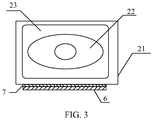
- FIG. 2 is a schematic view of a device assembly applied to a mobile terminal according to another embodiment of the present disclosure and FIG. 3 is a partially enlarged view of FIG. 2 .
- the device assembly further includes an interface 6 and an insulating layer 7 disposed between the interface 6 and the fingerprint tray 21.
- the interface 6 in the embodiment may be a USB interface of the mobile terminal, a headphone interface of the mobile terminal, etc., or an interface including the USB interface and the headphone interface.
- Number and type of the interface may be designed according to an internal circuit board of the mobile terminal, and the embodiment is not limited thereto.
- the interface 6 is the USB interface
- the interface 6 is used for connecting a charging circuit of the mobile terminal to an external charger.
- the insulating layer 7 is disposed between the fingerprint tray 21 and the interface 6, so that influence of the USB interface on the performance of the antenna assembly can be greatly reduced and reliability of the antenna assembly can be achieved.
- a length and an area of the first antenna 11 are greater than a length and an area of the second antenna 12, and therefore, the fingerprint assembly 2 in the embodiment of the present disclosure is disposed adjacent to the first antenna 11 and the first antenna 11 is disposed adjacent to the interface 6.
- the mobile terminal may further include an earphone socket 8 disposed between the first antenna 11 and the second antenna 12.
- the first antenna 11 and the second antenna 12 are reliably separated by the earphone socket 8.
- the antenna assembly further includes a third antenna 9, at least one feed point 10, and a first matching assembly 14, the third antenna 9 is connected to the circuit board 13 of the mobile terminal by the at least one feed point 10, the first matching assembly 14 is connected between the third antenna 9 and the circuit board 13 of the mobile terminal.
- the first matching assembly 14 may include a plurality of inductors and capacitances in series or in parallel, and inductance or capacitances of different inductive or capacitive branches may differ so that resonant frequencies of the different branches are different.
- the third antenna 9 may be combined with a different branch to cover different antenna bands.
- a second matching assembly 14a may also be connected in series between the feed point 10 and the third antenna 9.
- the structure and parameters of the mating assembly 14a may be the same as or different from the structure and parameters of the mating assembly 14, and the embodiment is not limited thereto.
- the first matching assembly 14 includes a plurality of matching branches and the antenna assembly includes a switch assembly 15 connected between the third antenna 9 and the first matching assembly 14 in order to make the antenna assembly cover different frequency according to the operation of the mobile terminal.
- the switch assembly 15 may include a plurality of switch devices connected in series to different matching branches, respectively to turn on or turn off the different matching branches.
- the switch assembly 15 may be a single-pole multiple-throw (SPMT) switch, and the switch assembly 15 operates in different states to conduct different matching branches.
- SPMT single-pole multiple-throw
- the embodiment of the present disclosure provides the device assembly applied to the mobile terminal.
- the device assembly includes the antenna assembly and the fingerprint assembly disposed adjacent to the antenna assembly.
- the fingerprint tray of the fingerprint assembly is electrically connected to the ground of the mobile terminal.
- the fingerprint module is connected to the fingerprint tray by the conductive assembly.
- the fingerprint assembly is efficiently and reliably connected to the ground of the mobile terminal, various non-linear effects generated by electromagnetic waves of the antenna assembly radiated on the fingerprint assembly are quickly returned to the ground of the mobile terminal, greatly reducing the impact caused by the fingerprint assembly occupying an antenna clearance area to the performance of the antenna assembly.
- the insulating layer disposed between the interface and the fingerprint tray, thereby greatly reducing the influence of the USB interface on the performance of the antenna assembly and ensuring the reliability of the antenna assembly.
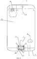
- FIG. 4 is a schematic view of a mobile terminal according to an embodiment of the present disclosure.
- the mobile terminal includes a fingerprint assembly 2, an antenna assembly, and a camera assembly 16.
- the camera assembly 16 may be disposed at any position of the mobile terminal, for example, the camera assembly 16 is disposed below the third antenna 9 shown in FIG. 4 .
- the camera assembly 16 divides an antenna clearance area corresponding to the third antenna 9 into different areas.
- the camera assembly 16 is also reliably connected to the ground of the mobile terminal, so as to ensure that various non-linear effects generated by electromagnetic waves of the antenna assembly radiated on the camera assembly are quickly returned to the ground of the mobile terminal, greatly reducing the impact of the camera assembly on the performance of the antenna assembly.
- a structure in which a first feature is "on" a second feature may include an embodiment in which the first feature directly contacts the second feature, and may also include an embodiment in which an additional feature is formed between the first feature and the second feature so that the first feature does not directly contact the second feature.
- a first feature "on,” “above,” or “on top of' a second feature may include an embodiment in which the first feature is right “on,” “above,” or “on top of' the second feature, and may also include an embodiment in which the first feature is not right “on,” “above,” or “on top of' the second feature, or just means that the first feature has a sea level elevation greater than the sea level elevation of the second feature.
- first feature "beneath,” “below,” or “on bottom of' a second feature may include an embodiment in which the first feature is right “beneath,” “below,” or “on bottom of' the second feature, and may also include an embodiment in which the first feature is not right “beneath,” “below,” or “on bottom of' the second feature, or just means that the first feature has a sea level elevation less than the sea level elevation of the second feature.
Landscapes
- Engineering & Computer Science (AREA)
- Computer Networks & Wireless Communication (AREA)
- Signal Processing (AREA)
- Human Computer Interaction (AREA)
- Physics & Mathematics (AREA)
- General Physics & Mathematics (AREA)
- Multimedia (AREA)
- Theoretical Computer Science (AREA)
- Telephone Set Structure (AREA)
- Support Of Aerials (AREA)
Claims (14)
- An einem mobilen Endgerät angewandte Geräteanordnung, umfassend eine Fingerabdruckanordnung (2), wobei die Fingerabdruckanordnung (2) umfasst:eine Fingerabdruckablage (21), die mit einer Masse (3) einer Leiterplatte (13) des mobilen Endgeräts elektrisch verbunden ist;ein Fingerabdruckmodul (22), das an der Fingerabdruckablage (21) angeordnet ist;eine leitende Anordnung (23);eine Schnittstelle (6); undeine Isolierschicht (7), dadurch gekennzeichnet, dass:
die leitende Anordnung (23) zwischen der Fingerabdruckablage (21) und dem Fingerabdruckmodul (22) angeordnet ist, das Fingerabdruckmodul (22) mit der Masse (3) der Leiterplatte (13) des mobilen Endgeräts durch die leitende Anordnung (23) und die Fingerabdruckablage (21) verbunden ist, und die Isolierschicht (7) zwischen der Schnittstelle (6) und der Fingerabdruckablage (21) angeordnet ist. - Geräteanordnung nach Anspruch 1, dadurch gekennzeichnet, dass sie ferner eine Antennenanordnung (1) umfasst, wobei die Fingerabdruckanordnung (2) in einer Fläche angeordnet ist, die von der Antennenanordnung (1) umschlossen ist.
- Geräteanordnung nach Anspruch 1 oder 2, dadurch gekennzeichnet, dass die leitende Anordnung (23) eine leitende Faser oder eine Kupferfolie ist.
- Geräteanordnung nach einem der Ansprüche 1-3, dadurch gekennzeichnet, dass die Antennenanordnung (1) eine erste Antenne (11), eine zweite Antenne (12) und eine mit der ersten Antenne (11) und der zweiten Antenne (12) verbundene Frequenzweiche (4) umfasst, und die Frequenzweiche (4) mit einer Antenneneinspeisung (5) der Leiterplatte (13) verbunden ist.
- Geräteanordnung nach Anspruch 4, dadurch gekennzeichnet, dass die erste Antenne (11) eine Niederfrequenz-Antenne ist, die zweite Antenne (12) eine Mittel- bis Hochfrequenz-Antenne ist, ein Frequenzbereich der ersten Antenne (11) in einem Bereich von 699 MHz bis 960 MHz liegt und ein Frequenzbereich der zweiten Antenne (12) in einem Bereich von 1710 MHz bis 2690 MHz liegt.
- Geräteanordnung nach Anspruch 4 oder 5, dadurch gekennzeichnet, dass eine Länge und eine Fläche der ersten Antenne (11) größer als eine Länge und eine Fläche der zweiten Antenne (12) sind.
- Geräteanordnung nach einem der Ansprüche 4-6, dadurch gekennzeichnet, dass sie ferner eine Ohrhörerbuchse (8) umfasst, die zwischen der ersten Antenne (11) und der zweiten Antenne (12) angeordnet ist, und die erste Antenne (11) und die zweite Antenne (12) durch die Ohrhörerbuchse (8) getrennt sind.
- Geräteanordnung nach einem der Ansprüche 1-7, dadurch gekennzeichnet, dass die Fingerabdruckablage (21) eine Metallablage ist.
- Geräteanordnung nach einem der Ansprüche 4-7, dadurch gekennzeichnet, dass die Fingerabdruckanordnung (2) benachbart zu der ersten Antenne (11) angeordnet ist.
- Geräteanordnung nach einem der Ansprüche 4-7, dadurch gekennzeichnet, dass die erste Antenne (11) benachbart zu der Schnittstelle (6) angeordnet ist.
- Geräteanordnung nach einem der Ansprüche 4-7, dadurch gekennzeichnet, dass die Antennenanordnung (1) ferner eine dritte Antenne (9), mindestens einen Einspeisungspunkt (10) und eine erste Anpassungsanordnung (14) umfasst, wobei die dritte Antenne (9) mit der Leiterplatte (13) des mobilen Endgeräts durch den mindestens einen Einspeisepunkt (10) verbunden ist, wobei die erste Anpassungsanordnung (14) zwischen der dritten Antenne (9) und der Leiterplatte (13) angeschlossen ist.
- Geräteanordnung nach Anspruch 11, dadurch gekennzeichnet, dass die Antennenanordnung (1) ferner eine zweite Anpassungsanordnung (14a) umfasst, die zwischen dem mindestens einen Einspeisepunkt (10) und der dritten Antenne (9) in Reihe angeschlossen ist.
- Geräteanordnung nach Anspruch 11 oder 12, dadurch gekennzeichnet, dass die Antennenanordnung (1) ferner eine Schalteranordnung (15) umfasst, die zwischen der dritten Antenne (9) und der ersten Anpassungsanordnung (14) angeschlossen ist.
- Mobiles Endgerät, umfassend:die Geräteanordnung nach einem der Ansprüche 11-13; undeine Kameraanordnung (16), die unter der dritten Antenne (9) angeordnet ist und mit der Masse (3) der Leiterplatte (13) verbunden ist.
Applications Claiming Priority (2)
| Application Number | Priority Date | Filing Date | Title |
|---|---|---|---|
| CN201621340419.2U CN206323420U (zh) | 2016-12-07 | 2016-12-07 | 应用于移动终端的设备组件及移动终端 |
| CN201611117055.6A CN106550073B (zh) | 2016-12-07 | 2016-12-07 | 应用于移动终端的设备组件及移动终端 |
Publications (2)
| Publication Number | Publication Date |
|---|---|
| EP3333972A1 EP3333972A1 (de) | 2018-06-13 |
| EP3333972B1 true EP3333972B1 (de) | 2020-01-08 |
Family
ID=59923297
Family Applications (1)
| Application Number | Title | Priority Date | Filing Date |
|---|---|---|---|
| EP17192056.4A Active EP3333972B1 (de) | 2016-12-07 | 2017-09-20 | An einem mobilen endgerät angewandte vorrichtungsanordnung und mobiles endgerät |
Country Status (4)
| Country | Link |
|---|---|
| US (1) | US10340590B2 (de) |
| EP (1) | EP3333972B1 (de) |
| ES (1) | ES2774490T3 (de) |
| WO (1) | WO2018103473A1 (de) |
Families Citing this family (2)
| Publication number | Priority date | Publication date | Assignee | Title |
|---|---|---|---|---|
| CN113675592B (zh) * | 2020-05-13 | 2023-08-04 | 北京小米移动软件有限公司 | 一种天线模组和终端设备 |
| CN112101143A (zh) * | 2020-08-27 | 2020-12-18 | 厦门厦华科技有限公司 | 一种用于指纹模块接地的极片及指纹装置 |
Citations (2)
| Publication number | Priority date | Publication date | Assignee | Title |
|---|---|---|---|---|
| US20090257626A1 (en) * | 2005-10-18 | 2009-10-15 | Authentec, Inc. | Thinned finger sensor and associated methods |
| US20150216024A1 (en) * | 2014-01-29 | 2015-07-30 | Apple Inc. | Electronic Devices Having Electrostatic Discharge Paths |
Family Cites Families (15)
| Publication number | Priority date | Publication date | Assignee | Title |
|---|---|---|---|---|
| WO2008075133A1 (en) | 2006-12-19 | 2008-06-26 | Nokia Corporation | An antenna arrangement |
| CN102348009A (zh) * | 2010-08-04 | 2012-02-08 | 鸿富锦精密工业(深圳)有限公司 | 具指纹识别功能的手机 |
| KR102013588B1 (ko) | 2012-09-19 | 2019-08-23 | 엘지전자 주식회사 | 이동 단말기 |
| KR102182297B1 (ko) * | 2014-01-13 | 2020-11-24 | 삼성전자 주식회사 | 지문을 인식하는 방법 및 이를 제공하는 휴대 단말기 |
| CN104079718B (zh) * | 2014-06-18 | 2016-09-28 | 京东方科技集团股份有限公司 | 具有指纹识别功能的个人移动终端设备 |
| US9577318B2 (en) | 2014-08-19 | 2017-02-21 | Apple Inc. | Electronic device with fingerprint sensor and tunable hybrid antenna |
| CN104732201B (zh) | 2015-01-07 | 2018-10-09 | 小米科技有限责任公司 | 触摸按键和指纹识别实现装置、方法及终端设备 |
| CN106155190A (zh) | 2015-04-13 | 2016-11-23 | 中兴通讯股份有限公司 | 一种支持nfc功能和指纹识别功能的装置和终端 |
| CN204760546U (zh) | 2015-06-12 | 2015-11-11 | 广东欧珀移动通信有限公司 | 天线系统及应用该天线系统的通信终端 |
| CN105488499B (zh) | 2016-01-18 | 2019-05-07 | 宸盛光电有限公司 | 一种指纹识别模组及具有该指纹识别模组的电子装置 |
| CN105828590A (zh) | 2016-05-10 | 2016-08-03 | 青岛海信移动通信技术股份有限公司 | 一种终端设备 |
| CN105870629A (zh) | 2016-05-23 | 2016-08-17 | 广东欧珀移动通信有限公司 | 一种终端天线及智能终端 |
| CN106127195B (zh) * | 2016-08-30 | 2017-11-17 | 广东欧珀移动通信有限公司 | 指纹模组、指纹模组制作方法及移动终端 |
| CN106550073B (zh) | 2016-12-07 | 2020-10-13 | Oppo广东移动通信有限公司 | 应用于移动终端的设备组件及移动终端 |
| CN206323420U (zh) | 2016-12-07 | 2017-07-11 | 广东欧珀移动通信有限公司 | 应用于移动终端的设备组件及移动终端 |
-
2017
- 2017-08-23 US US15/683,804 patent/US10340590B2/en active Active
- 2017-09-20 ES ES17192056T patent/ES2774490T3/es active Active
- 2017-09-20 EP EP17192056.4A patent/EP3333972B1/de active Active
- 2017-10-27 WO PCT/CN2017/108148 patent/WO2018103473A1/en not_active Ceased
Patent Citations (2)
| Publication number | Priority date | Publication date | Assignee | Title |
|---|---|---|---|---|
| US20090257626A1 (en) * | 2005-10-18 | 2009-10-15 | Authentec, Inc. | Thinned finger sensor and associated methods |
| US20150216024A1 (en) * | 2014-01-29 | 2015-07-30 | Apple Inc. | Electronic Devices Having Electrostatic Discharge Paths |
Also Published As
| Publication number | Publication date |
|---|---|
| US20180159212A1 (en) | 2018-06-07 |
| EP3333972A1 (de) | 2018-06-13 |
| ES2774490T3 (es) | 2020-07-21 |
| WO2018103473A1 (en) | 2018-06-14 |
| US10340590B2 (en) | 2019-07-02 |
Similar Documents
| Publication | Publication Date | Title |
|---|---|---|
| CN106550073B (zh) | 应用于移动终端的设备组件及移动终端 | |
| EP2885839B1 (de) | Antennenvorrichtung und herstellungsverfahren dafür | |
| US20150244063A1 (en) | Apparatus for wireless communication | |
| KR102664682B1 (ko) | 도전성 측면 부재를 이용한 안테나 및 그것을 포함하는 전자 장치 | |
| CN105703790B (zh) | 移动终端 | |
| JP2002151923A (ja) | 携帯端末機 | |
| CN106657467A (zh) | 移动终端 | |
| CN106252881B (zh) | 天线装置及移动终端 | |
| EP2962358B1 (de) | Vorrichtung und verfahren zur drahtlosen kopplung | |
| KR20210020667A (ko) | 비아 집단 패턴이 형성된 pcb 임베디드 필터를 포함하는 장치 및 인쇄 회로 기판 | |
| US20160329627A1 (en) | Embedded antenna | |
| EP3333972B1 (de) | An einem mobilen endgerät angewandte vorrichtungsanordnung und mobiles endgerät | |
| CN110797657B (zh) | 通信设备 | |
| CN206323420U (zh) | 应用于移动终端的设备组件及移动终端 | |
| KR20190024814A (ko) | 전자 디바이스의 하우징 및 전자 디바이스 | |
| CN102738555B (zh) | 手持式装置以及辐射场型调整方法 | |
| CN104795625A (zh) | 包含距离感应器的天线结构 | |
| CN106816707A (zh) | 电子装置 | |
| CN111755811A (zh) | 双频段天线 | |
| EP3333973A1 (de) | Mobiles endgerät | |
| CN106654573B (zh) | 射频天线装置 | |
| CN115441162B (zh) | 天线结构与电子装置 | |
| KR20210098764A (ko) | 안테나 모듈을 포함하는 전자 장치 | |
| US9343849B2 (en) | Electronic device and interface connector | |
| CN120149802A (zh) | 电子设备 |
Legal Events
| Date | Code | Title | Description |
|---|---|---|---|
| PUAI | Public reference made under article 153(3) epc to a published international application that has entered the european phase |
Free format text: ORIGINAL CODE: 0009012 |
|
| STAA | Information on the status of an ep patent application or granted ep patent |
Free format text: STATUS: REQUEST FOR EXAMINATION WAS MADE |
|
| 17P | Request for examination filed |
Effective date: 20170920 |
|
| AK | Designated contracting states |
Kind code of ref document: A1 Designated state(s): AL AT BE BG CH CY CZ DE DK EE ES FI FR GB GR HR HU IE IS IT LI LT LU LV MC MK MT NL NO PL PT RO RS SE SI SK SM TR |
|
| AX | Request for extension of the european patent |
Extension state: BA ME |
|
| STAA | Information on the status of an ep patent application or granted ep patent |
Free format text: STATUS: EXAMINATION IS IN PROGRESS |
|
| 17Q | First examination report despatched |
Effective date: 20180918 |
|
| RIC1 | Information provided on ipc code assigned before grant |
Ipc: H01Q 9/40 20060101ALI20190718BHEP Ipc: H01Q 21/30 20060101ALI20190718BHEP Ipc: G06F 21/32 20130101ALN20190718BHEP Ipc: H04M 1/02 20060101ALI20190718BHEP Ipc: G06K 9/00 20060101ALI20190718BHEP Ipc: H04B 1/00 20060101ALI20190718BHEP Ipc: H01Q 1/24 20060101AFI20190718BHEP |
|
| RIC1 | Information provided on ipc code assigned before grant |
Ipc: G06K 9/00 20060101ALI20190726BHEP Ipc: H01Q 9/40 20060101ALI20190726BHEP Ipc: H04M 1/02 20060101ALI20190726BHEP Ipc: G06F 21/32 20130101ALN20190726BHEP Ipc: H01Q 21/30 20060101ALI20190726BHEP Ipc: H01Q 1/24 20060101AFI20190726BHEP Ipc: H04B 1/00 20060101ALI20190726BHEP |
|
| GRAP | Despatch of communication of intention to grant a patent |
Free format text: ORIGINAL CODE: EPIDOSNIGR1 |
|
| STAA | Information on the status of an ep patent application or granted ep patent |
Free format text: STATUS: GRANT OF PATENT IS INTENDED |
|
| INTG | Intention to grant announced |
Effective date: 20190916 |
|
| GRAS | Grant fee paid |
Free format text: ORIGINAL CODE: EPIDOSNIGR3 |
|
| GRAA | (expected) grant |
Free format text: ORIGINAL CODE: 0009210 |
|
| STAA | Information on the status of an ep patent application or granted ep patent |
Free format text: STATUS: THE PATENT HAS BEEN GRANTED |
|
| RAP1 | Party data changed (applicant data changed or rights of an application transferred) |
Owner name: GUANGDONG OPPO MOBILE TELECOMMUNICATIONS CORP., LT |
|
| AK | Designated contracting states |
Kind code of ref document: B1 Designated state(s): AL AT BE BG CH CY CZ DE DK EE ES FI FR GB GR HR HU IE IS IT LI LT LU LV MC MK MT NL NO PL PT RO RS SE SI SK SM TR |
|
| REG | Reference to a national code |
Ref country code: GB Ref legal event code: FG4D |
|
| REG | Reference to a national code |
Ref country code: CH Ref legal event code: EP |
|
| REG | Reference to a national code |
Ref country code: DE Ref legal event code: R096 Ref document number: 602017010596 Country of ref document: DE |
|
| REG | Reference to a national code |
Ref country code: IE Ref legal event code: FG4D |
|
| REG | Reference to a national code |
Ref country code: AT Ref legal event code: REF Ref document number: 1223830 Country of ref document: AT Kind code of ref document: T Effective date: 20200215 |
|
| REG | Reference to a national code |
Ref country code: NL Ref legal event code: FP |
|
| REG | Reference to a national code |
Ref country code: LT Ref legal event code: MG4D |
|
| REG | Reference to a national code |
Ref country code: ES Ref legal event code: FG2A Ref document number: 2774490 Country of ref document: ES Kind code of ref document: T3 Effective date: 20200721 |
|
| PG25 | Lapsed in a contracting state [announced via postgrant information from national office to epo] |
Ref country code: LT Free format text: LAPSE BECAUSE OF FAILURE TO SUBMIT A TRANSLATION OF THE DESCRIPTION OR TO PAY THE FEE WITHIN THE PRESCRIBED TIME-LIMIT Effective date: 20200108 Ref country code: RS Free format text: LAPSE BECAUSE OF FAILURE TO SUBMIT A TRANSLATION OF THE DESCRIPTION OR TO PAY THE FEE WITHIN THE PRESCRIBED TIME-LIMIT Effective date: 20200108 Ref country code: PT Free format text: LAPSE BECAUSE OF FAILURE TO SUBMIT A TRANSLATION OF THE DESCRIPTION OR TO PAY THE FEE WITHIN THE PRESCRIBED TIME-LIMIT Effective date: 20200531 Ref country code: FI Free format text: LAPSE BECAUSE OF FAILURE TO SUBMIT A TRANSLATION OF THE DESCRIPTION OR TO PAY THE FEE WITHIN THE PRESCRIBED TIME-LIMIT Effective date: 20200108 Ref country code: NO Free format text: LAPSE BECAUSE OF FAILURE TO SUBMIT A TRANSLATION OF THE DESCRIPTION OR TO PAY THE FEE WITHIN THE PRESCRIBED TIME-LIMIT Effective date: 20200408 |
|
| PG25 | Lapsed in a contracting state [announced via postgrant information from national office to epo] |
Ref country code: IS Free format text: LAPSE BECAUSE OF FAILURE TO SUBMIT A TRANSLATION OF THE DESCRIPTION OR TO PAY THE FEE WITHIN THE PRESCRIBED TIME-LIMIT Effective date: 20200508 Ref country code: BG Free format text: LAPSE BECAUSE OF FAILURE TO SUBMIT A TRANSLATION OF THE DESCRIPTION OR TO PAY THE FEE WITHIN THE PRESCRIBED TIME-LIMIT Effective date: 20200408 Ref country code: SE Free format text: LAPSE BECAUSE OF FAILURE TO SUBMIT A TRANSLATION OF THE DESCRIPTION OR TO PAY THE FEE WITHIN THE PRESCRIBED TIME-LIMIT Effective date: 20200108 Ref country code: LV Free format text: LAPSE BECAUSE OF FAILURE TO SUBMIT A TRANSLATION OF THE DESCRIPTION OR TO PAY THE FEE WITHIN THE PRESCRIBED TIME-LIMIT Effective date: 20200108 Ref country code: HR Free format text: LAPSE BECAUSE OF FAILURE TO SUBMIT A TRANSLATION OF THE DESCRIPTION OR TO PAY THE FEE WITHIN THE PRESCRIBED TIME-LIMIT Effective date: 20200108 Ref country code: GR Free format text: LAPSE BECAUSE OF FAILURE TO SUBMIT A TRANSLATION OF THE DESCRIPTION OR TO PAY THE FEE WITHIN THE PRESCRIBED TIME-LIMIT Effective date: 20200409 |
|
| REG | Reference to a national code |
Ref country code: DE Ref legal event code: R097 Ref document number: 602017010596 Country of ref document: DE |
|
| PG25 | Lapsed in a contracting state [announced via postgrant information from national office to epo] |
Ref country code: DK Free format text: LAPSE BECAUSE OF FAILURE TO SUBMIT A TRANSLATION OF THE DESCRIPTION OR TO PAY THE FEE WITHIN THE PRESCRIBED TIME-LIMIT Effective date: 20200108 Ref country code: SM Free format text: LAPSE BECAUSE OF FAILURE TO SUBMIT A TRANSLATION OF THE DESCRIPTION OR TO PAY THE FEE WITHIN THE PRESCRIBED TIME-LIMIT Effective date: 20200108 Ref country code: EE Free format text: LAPSE BECAUSE OF FAILURE TO SUBMIT A TRANSLATION OF THE DESCRIPTION OR TO PAY THE FEE WITHIN THE PRESCRIBED TIME-LIMIT Effective date: 20200108 Ref country code: RO Free format text: LAPSE BECAUSE OF FAILURE TO SUBMIT A TRANSLATION OF THE DESCRIPTION OR TO PAY THE FEE WITHIN THE PRESCRIBED TIME-LIMIT Effective date: 20200108 Ref country code: SK Free format text: LAPSE BECAUSE OF FAILURE TO SUBMIT A TRANSLATION OF THE DESCRIPTION OR TO PAY THE FEE WITHIN THE PRESCRIBED TIME-LIMIT Effective date: 20200108 Ref country code: CZ Free format text: LAPSE BECAUSE OF FAILURE TO SUBMIT A TRANSLATION OF THE DESCRIPTION OR TO PAY THE FEE WITHIN THE PRESCRIBED TIME-LIMIT Effective date: 20200108 |
|
| PLBE | No opposition filed within time limit |
Free format text: ORIGINAL CODE: 0009261 |
|
| STAA | Information on the status of an ep patent application or granted ep patent |
Free format text: STATUS: NO OPPOSITION FILED WITHIN TIME LIMIT |
|
| REG | Reference to a national code |
Ref country code: AT Ref legal event code: MK05 Ref document number: 1223830 Country of ref document: AT Kind code of ref document: T Effective date: 20200108 |
|
| 26N | No opposition filed |
Effective date: 20201009 |
|
| PG25 | Lapsed in a contracting state [announced via postgrant information from national office to epo] |
Ref country code: AT Free format text: LAPSE BECAUSE OF FAILURE TO SUBMIT A TRANSLATION OF THE DESCRIPTION OR TO PAY THE FEE WITHIN THE PRESCRIBED TIME-LIMIT Effective date: 20200108 |
|
| PG25 | Lapsed in a contracting state [announced via postgrant information from national office to epo] |
Ref country code: PL Free format text: LAPSE BECAUSE OF FAILURE TO SUBMIT A TRANSLATION OF THE DESCRIPTION OR TO PAY THE FEE WITHIN THE PRESCRIBED TIME-LIMIT Effective date: 20200108 Ref country code: SI Free format text: LAPSE BECAUSE OF FAILURE TO SUBMIT A TRANSLATION OF THE DESCRIPTION OR TO PAY THE FEE WITHIN THE PRESCRIBED TIME-LIMIT Effective date: 20200108 |
|
| REG | Reference to a national code |
Ref country code: CH Ref legal event code: PL |
|
| REG | Reference to a national code |
Ref country code: BE Ref legal event code: MM Effective date: 20200930 |
|
| PG25 | Lapsed in a contracting state [announced via postgrant information from national office to epo] |
Ref country code: LU Free format text: LAPSE BECAUSE OF NON-PAYMENT OF DUE FEES Effective date: 20200920 |
|
| PG25 | Lapsed in a contracting state [announced via postgrant information from national office to epo] |
Ref country code: LI Free format text: LAPSE BECAUSE OF NON-PAYMENT OF DUE FEES Effective date: 20200930 Ref country code: IE Free format text: LAPSE BECAUSE OF NON-PAYMENT OF DUE FEES Effective date: 20200920 Ref country code: BE Free format text: LAPSE BECAUSE OF NON-PAYMENT OF DUE FEES Effective date: 20200930 Ref country code: CH Free format text: LAPSE BECAUSE OF NON-PAYMENT OF DUE FEES Effective date: 20200930 |
|
| PG25 | Lapsed in a contracting state [announced via postgrant information from national office to epo] |
Ref country code: TR Free format text: LAPSE BECAUSE OF FAILURE TO SUBMIT A TRANSLATION OF THE DESCRIPTION OR TO PAY THE FEE WITHIN THE PRESCRIBED TIME-LIMIT Effective date: 20200108 Ref country code: MT Free format text: LAPSE BECAUSE OF FAILURE TO SUBMIT A TRANSLATION OF THE DESCRIPTION OR TO PAY THE FEE WITHIN THE PRESCRIBED TIME-LIMIT Effective date: 20200108 Ref country code: CY Free format text: LAPSE BECAUSE OF FAILURE TO SUBMIT A TRANSLATION OF THE DESCRIPTION OR TO PAY THE FEE WITHIN THE PRESCRIBED TIME-LIMIT Effective date: 20200108 |
|
| PG25 | Lapsed in a contracting state [announced via postgrant information from national office to epo] |
Ref country code: MK Free format text: LAPSE BECAUSE OF FAILURE TO SUBMIT A TRANSLATION OF THE DESCRIPTION OR TO PAY THE FEE WITHIN THE PRESCRIBED TIME-LIMIT Effective date: 20200108 Ref country code: MC Free format text: LAPSE BECAUSE OF FAILURE TO SUBMIT A TRANSLATION OF THE DESCRIPTION OR TO PAY THE FEE WITHIN THE PRESCRIBED TIME-LIMIT Effective date: 20200108 Ref country code: AL Free format text: LAPSE BECAUSE OF FAILURE TO SUBMIT A TRANSLATION OF THE DESCRIPTION OR TO PAY THE FEE WITHIN THE PRESCRIBED TIME-LIMIT Effective date: 20200108 |
|
| PGFP | Annual fee paid to national office [announced via postgrant information from national office to epo] |
Ref country code: FR Payment date: 20221223 Year of fee payment: 7 |
|
| PGFP | Annual fee paid to national office [announced via postgrant information from national office to epo] |
Ref country code: IT Payment date: 20221227 Year of fee payment: 7 |
|
| P01 | Opt-out of the competence of the unified patent court (upc) registered |
Effective date: 20230412 |
|
| PGFP | Annual fee paid to national office [announced via postgrant information from national office to epo] |
Ref country code: NL Payment date: 20230403 Year of fee payment: 7 |
|
| PGFP | Annual fee paid to national office [announced via postgrant information from national office to epo] |
Ref country code: GB Payment date: 20230920 Year of fee payment: 7 |
|
| PGFP | Annual fee paid to national office [announced via postgrant information from national office to epo] |
Ref country code: DE Payment date: 20221222 Year of fee payment: 7 |
|
| PGFP | Annual fee paid to national office [announced via postgrant information from national office to epo] |
Ref country code: ES Payment date: 20231019 Year of fee payment: 7 |
|
| REG | Reference to a national code |
Ref country code: DE Ref legal event code: R119 Ref document number: 602017010596 Country of ref document: DE |
|
| REG | Reference to a national code |
Ref country code: NL Ref legal event code: MM Effective date: 20241001 |
|
| GBPC | Gb: european patent ceased through non-payment of renewal fee |
Effective date: 20240920 |
|
| PG25 | Lapsed in a contracting state [announced via postgrant information from national office to epo] |
Ref country code: NL Free format text: LAPSE BECAUSE OF NON-PAYMENT OF DUE FEES Effective date: 20241001 |
|
| PG25 | Lapsed in a contracting state [announced via postgrant information from national office to epo] |
Ref country code: DE Free format text: LAPSE BECAUSE OF NON-PAYMENT OF DUE FEES Effective date: 20250401 |
|
| PG25 | Lapsed in a contracting state [announced via postgrant information from national office to epo] |
Ref country code: GB Free format text: LAPSE BECAUSE OF NON-PAYMENT OF DUE FEES Effective date: 20240920 |
|
| PG25 | Lapsed in a contracting state [announced via postgrant information from national office to epo] |
Ref country code: IT Free format text: LAPSE BECAUSE OF NON-PAYMENT OF DUE FEES Effective date: 20240920 |
|
| PG25 | Lapsed in a contracting state [announced via postgrant information from national office to epo] |
Ref country code: FR Free format text: LAPSE BECAUSE OF NON-PAYMENT OF DUE FEES Effective date: 20240930 |
|
| REG | Reference to a national code |
Ref country code: ES Ref legal event code: FD2A Effective date: 20251031 |
|
| PG25 | Lapsed in a contracting state [announced via postgrant information from national office to epo] |
Ref country code: ES Free format text: LAPSE BECAUSE OF NON-PAYMENT OF DUE FEES Effective date: 20240921 |