EP3333887A1 - Interconnection structures and fabrication methods thereof - Google Patents
Interconnection structures and fabrication methods thereof Download PDFInfo
- Publication number
- EP3333887A1 EP3333887A1 EP17203761.6A EP17203761A EP3333887A1 EP 3333887 A1 EP3333887 A1 EP 3333887A1 EP 17203761 A EP17203761 A EP 17203761A EP 3333887 A1 EP3333887 A1 EP 3333887A1
- Authority
- EP
- European Patent Office
- Prior art keywords
- layer
- silicon
- conductive structure
- cap layer
- dielectric
- Prior art date
- Legal status (The legal status is an assumption and is not a legal conclusion. Google has not performed a legal analysis and makes no representation as to the accuracy of the status listed.)
- Withdrawn
Links
Images

Classifications
-
- H—ELECTRICITY
- H10—SEMICONDUCTOR DEVICES; ELECTRIC SOLID-STATE DEVICES NOT OTHERWISE PROVIDED FOR
- H10W—GENERIC PACKAGES, INTERCONNECTIONS, CONNECTORS OR OTHER CONSTRUCTIONAL DETAILS OF DEVICES COVERED BY CLASS H10
- H10W20/00—Interconnections in chips, wafers or substrates
- H10W20/40—Interconnections external to wafers or substrates, e.g. back-end-of-line [BEOL] metallisations or vias connecting to gate electrodes
- H10W20/45—Interconnections external to wafers or substrates, e.g. back-end-of-line [BEOL] metallisations or vias connecting to gate electrodes characterised by their insulating parts
- H10W20/47—Interconnections external to wafers or substrates, e.g. back-end-of-line [BEOL] metallisations or vias connecting to gate electrodes characterised by their insulating parts comprising two or more dielectric layers having different properties, e.g. different dielectric constants
-
- H—ELECTRICITY
- H10—SEMICONDUCTOR DEVICES; ELECTRIC SOLID-STATE DEVICES NOT OTHERWISE PROVIDED FOR
- H10P—GENERIC PROCESSES OR APPARATUS FOR THE MANUFACTURE OR TREATMENT OF DEVICES COVERED BY CLASS H10
- H10P14/00—Formation of materials, e.g. in the shape of layers or pillars
- H10P14/60—Formation of materials, e.g. in the shape of layers or pillars of insulating materials
- H10P14/63—Formation of materials, e.g. in the shape of layers or pillars of insulating materials characterised by the formation processes
- H10P14/6326—Deposition processes
- H10P14/6328—Deposition from the gas or vapour phase
- H10P14/6334—Deposition from the gas or vapour phase using decomposition or reaction of gaseous or vapour phase compounds, i.e. chemical vapour deposition
- H10P14/6339—Deposition from the gas or vapour phase using decomposition or reaction of gaseous or vapour phase compounds, i.e. chemical vapour deposition deposition by cyclic CVD, e.g. ALD, ALE or pulsed CVD
-
- H—ELECTRICITY
- H10—SEMICONDUCTOR DEVICES; ELECTRIC SOLID-STATE DEVICES NOT OTHERWISE PROVIDED FOR
- H10P—GENERIC PROCESSES OR APPARATUS FOR THE MANUFACTURE OR TREATMENT OF DEVICES COVERED BY CLASS H10
- H10P14/00—Formation of materials, e.g. in the shape of layers or pillars
- H10P14/60—Formation of materials, e.g. in the shape of layers or pillars of insulating materials
- H10P14/65—Formation of materials, e.g. in the shape of layers or pillars of insulating materials characterised by treatments performed before or after the formation of the materials
- H10P14/6502—Formation of materials, e.g. in the shape of layers or pillars of insulating materials characterised by treatments performed before or after the formation of the materials of treatments performed before formation of the materials
- H10P14/6512—Formation of materials, e.g. in the shape of layers or pillars of insulating materials characterised by treatments performed before or after the formation of the materials of treatments performed before formation of the materials by exposure to a gas or vapour
- H10P14/6514—Formation of materials, e.g. in the shape of layers or pillars of insulating materials characterised by treatments performed before or after the formation of the materials of treatments performed before formation of the materials by exposure to a gas or vapour by exposure to a plasma
-
- H—ELECTRICITY
- H10—SEMICONDUCTOR DEVICES; ELECTRIC SOLID-STATE DEVICES NOT OTHERWISE PROVIDED FOR
- H10P—GENERIC PROCESSES OR APPARATUS FOR THE MANUFACTURE OR TREATMENT OF DEVICES COVERED BY CLASS H10
- H10P14/00—Formation of materials, e.g. in the shape of layers or pillars
- H10P14/60—Formation of materials, e.g. in the shape of layers or pillars of insulating materials
- H10P14/66—Formation of materials, e.g. in the shape of layers or pillars of insulating materials characterised by the type of materials
- H10P14/668—Formation of materials, e.g. in the shape of layers or pillars of insulating materials characterised by the type of materials the materials being characterised by the deposition precursor materials
- H10P14/6681—Formation of materials, e.g. in the shape of layers or pillars of insulating materials characterised by the type of materials the materials being characterised by the deposition precursor materials the precursor containing a compound comprising Si
- H10P14/6682—Formation of materials, e.g. in the shape of layers or pillars of insulating materials characterised by the type of materials the materials being characterised by the deposition precursor materials the precursor containing a compound comprising Si the compound being a silane, e.g. disilane, methylsilane or chlorosilane
-
- H—ELECTRICITY
- H10—SEMICONDUCTOR DEVICES; ELECTRIC SOLID-STATE DEVICES NOT OTHERWISE PROVIDED FOR
- H10P—GENERIC PROCESSES OR APPARATUS FOR THE MANUFACTURE OR TREATMENT OF DEVICES COVERED BY CLASS H10
- H10P14/00—Formation of materials, e.g. in the shape of layers or pillars
- H10P14/60—Formation of materials, e.g. in the shape of layers or pillars of insulating materials
- H10P14/69—Inorganic materials
- H10P14/692—Inorganic materials composed of oxides, glassy oxides or oxide-based glasses
- H10P14/6921—Inorganic materials composed of oxides, glassy oxides or oxide-based glasses containing silicon
- H10P14/6928—Inorganic materials composed of oxides, glassy oxides or oxide-based glasses containing silicon the material containing silicon and at least one metal element, e.g. metal silicate based insulators or metal silicon oxynitrides
- H10P14/6929—Inorganic materials composed of oxides, glassy oxides or oxide-based glasses containing silicon the material containing silicon and at least one metal element, e.g. metal silicate based insulators or metal silicon oxynitrides the material containing aluminium, e.g. AlSiOx
-
- H—ELECTRICITY
- H10—SEMICONDUCTOR DEVICES; ELECTRIC SOLID-STATE DEVICES NOT OTHERWISE PROVIDED FOR
- H10P—GENERIC PROCESSES OR APPARATUS FOR THE MANUFACTURE OR TREATMENT OF DEVICES COVERED BY CLASS H10
- H10P14/00—Formation of materials, e.g. in the shape of layers or pillars
- H10P14/60—Formation of materials, e.g. in the shape of layers or pillars of insulating materials
- H10P14/69—Inorganic materials
- H10P14/692—Inorganic materials composed of oxides, glassy oxides or oxide-based glasses
- H10P14/6938—Inorganic materials composed of oxides, glassy oxides or oxide-based glasses the material containing at least one metal element, e.g. metal oxides, metal oxynitrides or metal oxycarbides
- H10P14/6939—Inorganic materials composed of oxides, glassy oxides or oxide-based glasses the material containing at least one metal element, e.g. metal oxides, metal oxynitrides or metal oxycarbides characterised by the metal
- H10P14/69391—Inorganic materials composed of oxides, glassy oxides or oxide-based glasses the material containing at least one metal element, e.g. metal oxides, metal oxynitrides or metal oxycarbides characterised by the metal the material containing aluminium, e.g. Al2O3
-
- H—ELECTRICITY
- H10—SEMICONDUCTOR DEVICES; ELECTRIC SOLID-STATE DEVICES NOT OTHERWISE PROVIDED FOR
- H10W—GENERIC PACKAGES, INTERCONNECTIONS, CONNECTORS OR OTHER CONSTRUCTIONAL DETAILS OF DEVICES COVERED BY CLASS H10
- H10W20/00—Interconnections in chips, wafers or substrates
- H10W20/01—Manufacture or treatment
- H10W20/031—Manufacture or treatment of conductive parts of the interconnections
- H10W20/056—Manufacture or treatment of conductive parts of the interconnections by filling conductive material into holes, grooves or trenches
-
- H—ELECTRICITY
- H10—SEMICONDUCTOR DEVICES; ELECTRIC SOLID-STATE DEVICES NOT OTHERWISE PROVIDED FOR
- H10W—GENERIC PACKAGES, INTERCONNECTIONS, CONNECTORS OR OTHER CONSTRUCTIONAL DETAILS OF DEVICES COVERED BY CLASS H10
- H10W20/00—Interconnections in chips, wafers or substrates
- H10W20/01—Manufacture or treatment
- H10W20/031—Manufacture or treatment of conductive parts of the interconnections
- H10W20/0698—Local interconnections
-
- H—ELECTRICITY
- H10—SEMICONDUCTOR DEVICES; ELECTRIC SOLID-STATE DEVICES NOT OTHERWISE PROVIDED FOR
- H10W—GENERIC PACKAGES, INTERCONNECTIONS, CONNECTORS OR OTHER CONSTRUCTIONAL DETAILS OF DEVICES COVERED BY CLASS H10
- H10W20/00—Interconnections in chips, wafers or substrates
- H10W20/01—Manufacture or treatment
- H10W20/071—Manufacture or treatment of dielectric parts thereof
- H10W20/074—Manufacture or treatment of dielectric parts thereof of dielectric parts comprising thin functional dielectric layers, e.g. dielectric etch-stop, barrier, capping or liner layers
- H10W20/075—Manufacture or treatment of dielectric parts thereof of dielectric parts comprising thin functional dielectric layers, e.g. dielectric etch-stop, barrier, capping or liner layers of multilayered thin functional dielectric layers
-
- H—ELECTRICITY
- H10—SEMICONDUCTOR DEVICES; ELECTRIC SOLID-STATE DEVICES NOT OTHERWISE PROVIDED FOR
- H10W—GENERIC PACKAGES, INTERCONNECTIONS, CONNECTORS OR OTHER CONSTRUCTIONAL DETAILS OF DEVICES COVERED BY CLASS H10
- H10W20/00—Interconnections in chips, wafers or substrates
- H10W20/01—Manufacture or treatment
- H10W20/071—Manufacture or treatment of dielectric parts thereof
- H10W20/074—Manufacture or treatment of dielectric parts thereof of dielectric parts comprising thin functional dielectric layers, e.g. dielectric etch-stop, barrier, capping or liner layers
- H10W20/077—Manufacture or treatment of dielectric parts thereof of dielectric parts comprising thin functional dielectric layers, e.g. dielectric etch-stop, barrier, capping or liner layers on sidewalls or on top surfaces of conductors
-
- H—ELECTRICITY
- H10—SEMICONDUCTOR DEVICES; ELECTRIC SOLID-STATE DEVICES NOT OTHERWISE PROVIDED FOR
- H10W—GENERIC PACKAGES, INTERCONNECTIONS, CONNECTORS OR OTHER CONSTRUCTIONAL DETAILS OF DEVICES COVERED BY CLASS H10
- H10W20/00—Interconnections in chips, wafers or substrates
- H10W20/40—Interconnections external to wafers or substrates, e.g. back-end-of-line [BEOL] metallisations or vias connecting to gate electrodes
- H10W20/41—Interconnections external to wafers or substrates, e.g. back-end-of-line [BEOL] metallisations or vias connecting to gate electrodes characterised by their conductive parts
- H10W20/435—Cross-sectional shapes or dispositions of interconnections
-
- H—ELECTRICITY
- H10—SEMICONDUCTOR DEVICES; ELECTRIC SOLID-STATE DEVICES NOT OTHERWISE PROVIDED FOR
- H10W—GENERIC PACKAGES, INTERCONNECTIONS, CONNECTORS OR OTHER CONSTRUCTIONAL DETAILS OF DEVICES COVERED BY CLASS H10
- H10W20/00—Interconnections in chips, wafers or substrates
- H10W20/40—Interconnections external to wafers or substrates, e.g. back-end-of-line [BEOL] metallisations or vias connecting to gate electrodes
- H10W20/41—Interconnections external to wafers or substrates, e.g. back-end-of-line [BEOL] metallisations or vias connecting to gate electrodes characterised by their conductive parts
- H10W20/44—Conductive materials thereof
- H10W20/4403—Conductive materials thereof based on metals, e.g. alloys, metal silicides
- H10W20/4421—Conductive materials thereof based on metals, e.g. alloys, metal silicides the principal metal being copper
-
- H—ELECTRICITY
- H10—SEMICONDUCTOR DEVICES; ELECTRIC SOLID-STATE DEVICES NOT OTHERWISE PROVIDED FOR
- H10W—GENERIC PACKAGES, INTERCONNECTIONS, CONNECTORS OR OTHER CONSTRUCTIONAL DETAILS OF DEVICES COVERED BY CLASS H10
- H10W20/00—Interconnections in chips, wafers or substrates
- H10W20/40—Interconnections external to wafers or substrates, e.g. back-end-of-line [BEOL] metallisations or vias connecting to gate electrodes
- H10W20/41—Interconnections external to wafers or substrates, e.g. back-end-of-line [BEOL] metallisations or vias connecting to gate electrodes characterised by their conductive parts
- H10W20/44—Conductive materials thereof
- H10W20/4451—Semiconductor materials, e.g. polysilicon
-
- H—ELECTRICITY
- H10—SEMICONDUCTOR DEVICES; ELECTRIC SOLID-STATE DEVICES NOT OTHERWISE PROVIDED FOR
- H10W—GENERIC PACKAGES, INTERCONNECTIONS, CONNECTORS OR OTHER CONSTRUCTIONAL DETAILS OF DEVICES COVERED BY CLASS H10
- H10W20/00—Interconnections in chips, wafers or substrates
- H10W20/01—Manufacture or treatment
- H10W20/071—Manufacture or treatment of dielectric parts thereof
- H10W20/093—Manufacture or treatment of dielectric parts thereof by modifying materials of the dielectric parts
- H10W20/097—Manufacture or treatment of dielectric parts thereof by modifying materials of the dielectric parts by thermally treating
Definitions
- the present invention generally relates to the field of semiconductor fabrication technology and, more particularly, relates to interconnection structures and fabrication methods thereof.
- interconnection structures are usually used to connect different metal layers or connect a metal layer with a substrate.
- the dimension of interconnection structures also becomes smaller and smaller.
- a first aspect of the present invention provides a method for fabricating an interconnection structure.
- the method includes providing a substrate, forming a dielectric layer on the substrate, forming a conductive structure in the dielectric layer, forming a cap layer doped with silicon on the conductive structure and the dielectric layer, and performing an annealing process on the conductive structure and the cap layer.
- the cap layer is made of a material including silicon-doped AlN.
- the cap layer is formed by an atomic layer deposition.
- an atomic percentage of the silicon doped in the cap layer is in a range of approximately 10% to approximately 20%.
- the method further includes: controlling a doping concentration of the silicon in the cap layer to gradually decrease along a direction away from the conductive structure.
- forming the cap layer further includes at least one time of deposition of a silicon-doped material.
- each time of the deposition of the silicon-doped material includes absorbing an Al-containing atomic layer, absorbing a Si-containing atomic layer on the Al-containing atomic layer, and performing a nitrogen treatment process on the Al-containing atomic layer and the Si-containing atomic layer.
- absorbing the Si-containing atomic layer on the Al-containing atomic layer includes introducing a Si-containing reaction gas including SiH4, and removing remaining Si-containing reaction gas by purging.
- deposition of the silicon-doped material is performed multiple times.
- a flow rate of SiH4 gradually decreases during the multiple times of deposition of the silicon-doped material.
- deposition of the silicon-doped material is performed for multiple times.
- a process time to introduce SiH4 gradually decreases during the multiple times of the deposition of the silicon-doped material.
- the cap layer has a bi-layer structure, and wherein forming the cap layer further includes: forming an AlSiN layer on the conductive structure and the dielectric layer; and forming an AlN layer on the AlSiN layer.
- the ratio between a thickness of the AlSiN layer and a thickness of the AlN layer is in a range of 3:1 to 2:1.
- the cap layer further including: performing a plasma pre-treatment process on a surface of the dielectric layer.
- performing the plasma pre-treatment process includes: using plasma of trisilylamine to treat the surface of the dielectric layer.
- the dielectric layer is made of an ultra-low-k dielectric material with a dielectric constant lower than 2.5.
- the conductive structure is made of Cu.
- a second aspect of the present invention provides an interconnection structure.
- the interconnection structure includes a substrate, a dielectric layer formed on the substrate, a conductive structure formed in the dielectric layer, and a cap layer doped with silicon and formed on the conductive structure and the dielectric layer.
- the cap layer is made of a material including silicon-doped AlN.
- an atomic percentage of the silicon doped in the cap layer is in a range of approximately 10% to approximately 20%.
- a doping concentration of silicon in the cap layer gradually decreases.
- the cap layer has a bi-layer structure including: an AlSiN layer; and an AlN layer formed on the AlSiN layer.
- the ratio between a thickness of the AlSiN layer and a thickness of the AlN layer is in a range of 3:1 to 2:1.
- the dielectric layer is made of an ultra-low-k dielectric material with a dielectric constant lower than 2.5.
- the conductive structure is made of Cu.
- a interconnections structure according to the second aspect of the present invention may be obtained by a method according to the first aspect of the present invention.
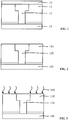
- FIG. 1 illustrates a schematic cross-section view of an interconnection structure.
- the interconnection structure includes a substrate 10, a dielectric layer 11 formed on the substrate 10, a conductive structure 12 formed in the dielectric layer 11, and a cap layer 13 formed on the dielectric layer 11 and the conductive structure 12.
- the conductive structure further includes a plug (not shown) and an interconnection (not shown) formed on the plug.
- the cap layer 13 is used to suppress the emergence of the EM phenomenon in the conductive structure 12.
- the cap layer 13 is made of AlN.
- the AlN-made cap layer 13 may also serve as an etch stop layer during the fabrication process of the interconnection structure.
- the fabrication process for the AlN-made cap layer 13 often faces two problems.
- the strength of the connection between the AlN-made cap layer 13 and the conductive structure 12 may be relatively weak, and thus the ability of the AlN-made cap layer 13 to suppress the EM phenomenon may be weak.
- the ability of the AlN-made cap layer 13 in suppressing the EM phenomenon may often be one to two orders of magnitude weaker.
- the dielectric layer 11 may have a relatively low density and may contain a plurality of pores. Therefore, during the process to form the AlN-made cap layer 13, the Al atoms may easily penetrate through and enter the pores of the dielectric layer 11. Therefore, the electrical isolation properties of the dielectric layer 11 may be reduced, and the possibility for current leaking or time dependent dielectric breakdown (TDDB) to take place may be increased.
- TDDB time dependent dielectric breakdown
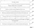
- FIG. 7 illustrates a flowchart of an exemplary method for fabricating an interconnection structure consistent with various disclosed embodiments in the present invention.
- FIG. 2 shows a schematic cross-section view of a semiconductor structure consistent with various embodiments of the present invention.
- a substrate 100 maybe provided.
- the substrate 100 may be used to provide a basis for process operation.
- the substrate 100 is made of single-crystalline silicon.
- the substrate may be made of polycrystalline silicon, amorphous silicon, germanium, SiGe, GaAs, or any other appropriate semiconductor material.
- the substrate may also be a structure with an epitaxial layer or a structure with silicon formed on an epitaxial layer.
- the substrate 100 is a planar substrate.
- the substrate may include a plurality of semiconductor structures, such as fin structures, etc. formed on the substrate.
- a dielectric layer may be formed on the substrate (S302). As shown in FIG. 2 , a dielectric layer 110 maybe formed on the substrate 100. The dielectric layer 110 may be used to electrically isolate neighboring semiconductor structures. In one embodiment, the dielectric layer 110 is an interlayer dielectric layer used to electrically isolate neighboring device layers.
- the dielectric layer 110 may be made of an ultra-low-k dielectric material (i.e., a material with a dielectric constant less than 2.5), such as doped SiO 2 , organic polymers, porous materials, etc. Therefore, the dielectric layer 110 may contain a plurality of pores, and thus may have a relatively low density.
- an ultra-low-k dielectric material i.e., a material with a dielectric constant less than 2.5
- the dielectric layer 110 may contain a plurality of pores, and thus may have a relatively low density.
- the dielectric layer may be made of one or more from SiO x , SiN x , SiON, low-k dielectric materials (i.e., materials with a dielectric constant greater than or equal to 2.5, but less than 3.9), and ultra-low-k dielectric materials.
- the dielectric layer 110 may be formed by various methods including chemical vapor deposition (CVD), physical vapor deposition (PVD), atomic layer deposition (ALD), furnace tube deposition, etc.
- CVD chemical vapor deposition
- PVD physical vapor deposition
- ALD atomic layer deposition
- furnace tube deposition etc.
- a conductive structure may be formed in the dielectric layer (S303).
- a conductive structure 120 may be formed in the dielectric layer 110.
- the conductive structure 120 may be used to make a connection from a semiconductor structure formed in the substrate 100 to an external circuit.
- the conductive structure 120 may penetrate through the dielectric layer 110 and directly connect to the substrate 100. Therefore, the conductive structure 120 may be used to make the connection between the substrate 100 and the external circuit.
- the conductive structure 120 may be formed in the dielectric layer 110 and may not be connected to the substrate 100.
- the interconnection structure may be a dual Damascene structure. Therefore, the conductive structure 120 may include a plug (not shown) formed on the substrate 100 and an interconnection (not shown) formed on the plug. In other embodiments, the interconnection structure may be a single Damascene structure or any other form of interconnection structure. Moreover, the conductive structure 120 may be made of copper.
- the process to form the conductive structure 120 may include the following steps. First, an opening may be formed in the dielectric layer 110.
- the opening may include a trench and a through hole.
- the trench may be formed through a top portion of the dielectric layer 110. That is, the trench may be formed by removing a top portion of the dielectric layer 110.
- the through hole may be formed on the bottom of the trench and may penetrate through the remaining portion of the dielectric layer 110.
- the conductive structure 120 may be formed in the opening.
- the process to form the conductive structure 120 in the opening may further include forming a conductive layer to cover the dielectric layer 110 by filling the opening with a conductive material, and performing a planarization process on the conductive layer to remove the portion of the conductive layer formed above the dielectric layer 110, and thus form the conductive structure 120.
- the fabrication method may also include removing the oxide formed on the surface of the conductive structure 120 by using a nitrogen-containing gas to treat the conductive structure 120.
- the nitrogen-containing gas may include at least one of NH 3 and N 2 .
- FIG. 3 shows a schematic diagram of performing a plasma pre-treatment process according to various embodiments of the present invention.
- the fabrication method may further include performing a plasma pre-treatment process 200 on the surface of the dielectric layer 110.
- the dielectric layer 110 may be made of an ultra-low-k dielectric material with a relatively low density.
- the plasma pre-treatment process 200 may be used to repair the defects on the surface of the dielectric layer 110 and improve the density of the dielectric layer 110. Therefore, during a subsequent process to form a cap layer, diffusion of the material of the cap layer into the dielectric layer 110 may be suppressed, and thus the emergence of current leaking and the TDDB phenomenon may be reduced.
- trisilylamine Si 3 H 9 N, TSA
- TSA trisilylamine
- TSA may be used in the plasma pre-treatment process 200 to treat the surface of the dielectric layer 110.
- TSA may be dissociated into Si atoms and N atoms.
- the Si atoms and the N atoms in TSA may locally react with the dielectric layer 110 and form chemical bonds, i.e. Si-O-SiN bonds, to repair the defects at the surface of the dielectric layer 110 and improve the density of the dielectric layer 110.
- the electrical isolation performance of the dielectric layer 110 in the formed interconnection structure may be improved, and the emergence of current leaking and the TDDB phenomenon may be reduced. Therefore, the reliability of the formed interconnection structure may be improved.
- TSA may be used to treat the surface of the dielectric layer 110 during the plasma pre-treatment process 200.
- the process parameters used in the plasma pre-treatment process 200 may include a flow rate of the TSA-containing process gas in a range of approximately 150 sccm to 300 sccm, an RF power in a range of approximately 250 W and 750 W, a process temperature in a range of approximately 250 °C to 350 °C, a process gas pressure in a range of approximately 3 Torr to 10 Torr, and a pre-treatment time in a range of approximately 15 s to 45 s.
- a cap layer may be formed on the conductive structure and the dielectric layer.
- the cap layer may be used to improve the connection strength between the conductive structure 120 and the dielectric layer 110, and thus suppress the EM in the formed interconnection structure. As such, the reliability of the formed interconnection structure may be improved.
- the cap layer may have a multi-layer structure.
- the cap layer may include an AlSiN layer and an AlN layer formed on the AlSiN layer.
- the cap layer may have a single layer structure.
- the cap layer may have a signal layer structure made of AlSiN.
- an AlSiN layer may be formed on the conductive structure and the dielectric layer (S305).
- FIG. 4 shows a schematic view of a corresponding semiconductor structure.
- an AlSiN layer 131 may be formed on the conductive structure 120 and the dielectric layer 110.
- the AlSiN layer 131 may be formed by an ALD process.
- films formed by an ALD process may demonstrate desired step coverage. Therefore, forming the AlSiN layer 131 through an ALD process may be able to efficiently improve the morphology of the formed cap layer and thus conducive to increasing the process window and improve the product yield.
- the process to form the AlSiN layer 131 may include performing at least one deposition of a Si-doped material.
- the process to deposit the Si-doped material may include absorbing an aluminum-containing atomic layer, absorbing a silicon-containing atomic layer on the aluminum-containing atomic layer, and then performing a nitrogen treatment process on the aluminum-containing atomic layer and the silicon-containing atomic layer.
- the process to absorb the aluminum-containing atomic layer may include introducing an aluminum-containing reaction gas pulse for deposition, and then removing the residual of the aluminum-containing reaction gas through purging.
- the aluminum-containing gas may be trimethylaluminum (TMA), i.e. AlCH 3 .
- the flow rate of the aluminum-containing reaction gas may be in a range of approximately 50 sccm to 150 sccm
- the gas pressure may be in a range of approximately 5 Torr to 15 Torr
- the process temperature may be in a range of approximately 250 °C to 350 °C
- the process time may be in a range of approximately 10 ms to 50 ms.
- the process to remove the residual of the aluminum-containing reaction gas may include introducing an inert gas to purge the residual of the aluminum-containing reaction gas.
- the inert gas may be Ar, and during the process to purge the residual of the aluminum-containing reaction gas, the flow rate of the inert gas may be in a range of approximately 50 sccm to 150 sccm, the gas pressure may be in a range of approximately 3 Torr to 5 Torr, and the process time may be in a range of approximately 50 ms to 150 ms.
- the process to absorb the silicon-containing atomic layer on the aluminum-containing atomic layer may include introducing a silicon-containing reaction gas pulse for deposition, and then removing the residual of the silicon-containing gas through purging.
- the silicon-containing gas may include SiH 4 .
- the flow rate of the silicon-containing reaction gas may be in a range of approximately 50 sccm to 150 sccm
- the gas pressure may be in a range of approximately 5 Torr to 15 Torr
- the process temperature may be in a range of approximately 250 °C to 350 °C
- the process time may be in a range of approximately 10 ms to 50ms.
- the process to remove the residual of the silicon-containing reaction gas may include introducing an inert gas to purge the residual of the silicon-containing reaction gas.
- the inert gas may be Ar, and during the process to purge the residual of the silicon-containing reaction gas, the flow rate of the inert gas may be in a range of approximately 50 sccm to 150 sccm, the gas pressure may be in a range of approximately 3 Torr to 5 Torr, and the process time may be in a range of approximately 50 ms to 150 ms.
- the nitrogen treatment performed on the aluminum-containing atomic layer and the silicon-containing atomic layer may include using a nitrogen-containing reaction gas to treat the aluminum-containing atomic layer and the silicon-containing atomic layer.
- the nitrogen-containing reaction gas may include at least one of NH 3 and N 2 .
- the flow rate of the nitrogen may be in a range of approximately 100 sccm to 200 sccm
- the gas pressure may be in a range of approximately 5 Torr to 15 Torr
- a process temperature may be in a range of approximately 250 °C to 350 °C
- a process time may be in a range of approximately 50 ms to 150 ms.
- the doping concentration of silicon in the AlSiN layer 131 may not be too high or too low.
- the doping concentration of silicon in the AlSiN layer 131 is too low, the Si atoms that can react with the material of the dielectric layer 110 and form chemical bonds may not be sufficient so that the connection strength between the dielectric layer 110 and the conductive structure 120 may not be effectively improved. Therefore, such a low doping concentration of silicon in the AlSiN layer 131 may not be conducive to improving the reliability of the formed interconnection structure.
- the doping concentration of silicon in the AlSiN layer 131 may be in a range of approximately 10% to 20%.
- the AlSiN layer 131 may be formed by a process including multiple times of deposition of a silicon-doped material. That is, the absorption of an aluminum-containing atomic layer, the absorption of a silicon-containing atomic layer, and the nitrogen treatment process may be repeatedly executed until the thickness of the formed AlSiN layer 131 reaches a preset value.
- the doping concentration of silicon in the AlSiN layer 131 may affect the resistance of the subsequently-formed cap layer.
- Si atoms maybe able to combine with Cu atoms and form chemical bonds only when the Si atoms are on the surface of the conductive structure 120. Therefore, in one embodiment, during the process to form the AlSiN layer 131, in order to reduce the resistance of the subsequently-formed cap layer, the doping concentration of silicon in the AlSiN layer 131 may gradually decrease along the direction away from the conductive structure 120. As such, the influence on the electrical performance of the interconnection structure due to the formation of the silicon-doped cap layer may be reduced, and thus the performance and the reliability of the formed interconnection structure may be improved.
- the multiple times of deposition of the silicon-doped material may include a gradually reduced flow rate of SiH 4 , or a gradually reduced process time for introducing SiH 4 .
- the reduction of the flow rate of SiH 4 in each step may not be too large or too small.
- the doping concentration of silicon in the formed AlSiN layer 131 may become too small such that the connection strength between the dielectric layer 110 and the conductive structure 120 may not be effectively improved. Therefore, such a large reduction of the flow rate of SiH 4 in each step may not be conducive to improving the reliability of the formed interconnection structure.
- the flow rate of SiH 4 may be gradually reduced from an initial flow rate to approximately 25% of the initial flow rate. That is, during the last deposition of the silicon-doped material, the flow rate of SiH 4 may be approximately 25% of the initial flow rate.
- the reduction of the process time to introduce SiH 4 in each step may not be too large or too small.
- the doping concentration of silicon in the formed AlSiN layer 131 may become too small such that the connection strength between the dielectric layer 110 and the conductive structure 120 may not be effectively improved. Therefore, such a large reduction of the process time to introduce SiH 4 in each step may not be conducive to improving the reliability of the formed interconnection structure.
- the process time to introduce SiH 4 may be gradually reduced from an initial process time to approximately 25% of the initial process time. That is, during the last deposition of the silicon-doped material, the process time to introduce SiH 4 may be approximately 25% of the initial process time.
- the thickness of the formed AlSiN layer 131 may not be too large or too small.
- the connection strength between the conductive structure 120 and the dielectric layer 110 may not be effectively improved, which may further affect the improvement of the reliability of the interconnection structure.
- the overly large thickness of the AlSiN layer 131 may lead to problems such as material waste and increased process challenges.
- an overly large total thickness of the Si-doped cap layer 131 may also lead to an overly large resistance for the subsequently-formed cap layer, and further affect the electrical performance of the formed interconnection structure.
- the thickness of the AlSiN layer 131 may be in a range of approximately 20 ⁇ to 50 ⁇ .
- FIG. 5 shows a schematic cross-section view of a corresponding semiconductor structure.
- an AlN layer 132 may be formed on the top of the AlSiN layer 131.
- the AlN layer 132 and the AlSiN layer 131 may together form a cap layer 130.
- the AlN layer 132 may be formed by an ALD process. Specifically, films formed by an ALD process may demonstrate desired step coverage. Therefore, forming the AlN layer 132 through an ALD process may be able to efficiently improve the morphology of the formed cap layer 130 and thus conducive to increasing the process window and improve the product yield.
- the process to form the AlN layer 132 may include performing at least one deposition.
- the deposition process may include absorbing an aluminum-containing atomic layer and then performing a nitrogen treatment process on the aluminum-containing atomic layer.
- the process to absorb the aluminum-containing atomic layer may include introducing an aluminum-containing reaction gas pulse for deposition, and removing the residual of the aluminum-containing reaction gas through purging.
- the aluminum-containing gas may be AlCH 3 (i.e. TMA).
- the flow rate of the aluminum-containing reaction gas may be in a range of approximately 50 sccm to 150 sccm
- the gas pressure may be in a range of approximately 5 Torr to 15 Torr
- the process temperature may be in a range of approximately 250 °C to 350 °C
- the process time may be in a range of approximately 10 ms to 50ms.
- the process to remove the residual of the aluminum-containing reaction gas may include introducing an inert gas to purge the residual of the aluminum-containing reaction gas.
- the inert gas may be Ar, and during the process to purge the residual of the aluminum-containing reaction gas, the flow rate of the inert gas may be in a range of approximately 50 sccm to 150 sccm, the gas pressure may be in a range of approximately 3 Torr to 5 Torr, and the process time may be in a range of approximately 50 ms to 150 ms.
- the Si atoms in the cap layer 130 may react with the material of the conductive structure 120 and form chemical bonds. Therefore, the connection strength between the cap layer 130 and the conductive structure 120 may be improved, which may be conducive to suppressing the EM in the formed interconnection structure, and thus may help improve the reliability of the formed interconnection structure.
- the cap layer 130 may be made of a material including Si-doped AlN, and the conductive structure 120 may be made of copper.
- the Si atoms doped in the cap layer 130 may be able to react with the Al atoms and the N atoms in the cap layer 130 as well as the Cu atoms in the conductive structure 120, and further form chemical bonds, i.e. CuSi-AlN bonds. Therefore, the connection strength between the cap layer 130 and the conductive structure 120 may be improved. As such, the EM in the formed interconnection structure may be suppressed and the reliability of the formed interconnection structure may be improved.
- the nitrogen treatment performed on the aluminum-containing atomic layer may include using a nitrogen-containing reaction gas to treat the aluminum-containing atomic layer.
- the nitrogen-containing reaction gas may include at least one of NH 3 and N 2 .
- the flow rate of the nitrogen may be in a range of approximately 100 sccm to 200 sccm
- the gas pressure may be in a range of approximately 5 Torr to 15 Torr
- a process temperature may be in a range of approximately 250 °C to 350 °C
- a process time may be in a range of approximately 50 ms to 150 ms.
- the AlN layer 132 may be formed by a process including multiple times of material deposition. That is, the absorption of an aluminum-containing atomic layer and the nitrogen treatment process may be repeatedly executed until the thickness of the formed AlN layer 132 reaches a preset value.
- the thickness of the formed AlN layer 132 may not be too large or too small.
- the connection strength between the conductive structure 120 and the dielectric layer 110 may not be effectively improved, which may further affect the improvement of the reliability of the interconnection structure.
- the thickness of the AlN layer 132 is too large, the overly large thickness of the AlN layer 132 may lead to problems such as material waste and increased process challenges.
- the thickness of t AlN layer 132 may be in a range of approximately 5 ⁇ to 25 ⁇ .
- the ratio between the thickness of the AlSiN layer 131 and the thickness of the AlN layer 132 may not be too large or too small.
- the Si doping concentration in the cap layer 130 may be too small to effectively improve the connection strength between the conductive structure 120 and the dielectric layer 110, and thus may affect the reliability of the interconnection structure.
- the ratio between the thickness of the AlSiN layer 131 and the thickness of the AlN layer 132 is too large, the large ratio may lead to material waste and increased process challenges.
- the overly large doping concentration of Si in the cap layer 130 may also cause the resistance of the formed cap layer 130 to be too large, and thus the electrical performance of the formed interconnection structure may be affected.
- the ratio between the thickness of the AlSiN layer 131 and the thickness of the AlN layer 132 may be in a range from approximately 3:1 to approximately 2:1.
- FIG. 6 shows a schematic diagram of an annealing process according to various embodiments of the present invention.
- an annealing process 210 may be performed on the conductive structure 210 and the cap layer 130.
- the annealing process 210 may be used to form an interconnection structure.
- the annealing process 210 may also be used to enable the diffusion of the Si atoms in the cap layer 130, and thus allow the Si atoms further to react with the atoms in the material of the conductive structure 120 and form chemical bonds. As such, the emergence of the EM phenomenon in the formed interconnection structure may be suppressed, and the reliability of the formed interconnection structure may be improved.
- the conductive structure 120 is made of copper
- the cap layer 130 is made of a material including Si-doped AlN.
- the annealing process 210 may enable the diffusion of the Si atoms in the cap layer 130 diffuse and further allow the Si atoms to react with the Al atoms and the N atoms in the cap layer 130 as well as the Cu atoms in the conductive structure 120 and form chemical bonds, i.e. CuSi-AlN bonds.
- the connection strength between the cap layer 130 and the conductive structure 120 may be improved. Therefore, performing the annealing process may help improving the connection strength between the cap layer 130 and the conductive structure 120, suppressing the EM in the formed interconnection structure, and also improving the reliability of the formed interconnection structure.
- the anneal temperature may not be too high or too low, and the anneal time may not be too long or too short.
- the anneal temperature may be in a range of approximately 250 °C to 350 °C, and the anneal time may be in a range of approximately 2 minutes to 5 minutes.
- the fabricating method may also include forming a dielectric cap layer on the cap layer 130.
- the dielectric cap layer may be formed by any appropriate method according to current technology.
- FIG. 6 illustrates an exemplary interconnection structure according to various embodiments of the present invention.
- the interconnection structure may include a substrate 100, a dielectric layer 110 formed on the substrate 100, a conductive structure 120 formed in the dielectric layer 110, a cap layer 130 formed on the conductive structure 120 and the dielectric layer 110.
- the cap layer 130 may be a Si-doped cap layer.
- the substrate 100 is made of single-crystalline silicon.
- the substrate may also be made of polycrystalline silicon, amorphous silicon, germanium, SiGe, GaAs, or any other appropriate semiconductor material.
- the substrate may also be a structure with an epitaxial layer or a structure with silicon formed on an epitaxial layer.
- the substrate 100 is a planar substrate.
- the substrate may also include a plurality of semiconductor structures, such as fin structures, etc. formed on the substrate.
- the dielectric layer 110 may be made of an ultra-low-k dielectric material (i.e., a material with a dielectric constant less than 2.5), such as doped SiO 2 , organic polymers, porous materials, etc. Therefore, the dielectric layer 110 may contain a plurality of pores, and thus may have a relatively low density.
- an ultra-low-k dielectric material i.e., a material with a dielectric constant less than 2.5
- the dielectric layer 110 may contain a plurality of pores, and thus may have a relatively low density.
- the dielectric layer may also be made of one or more from SiO x , SiN x , SiON, low-k dielectric materials (i.e., materials with a dielectric constant greater than or equal to 2.5, but less than 3.9), and ultra-low-k dielectric materials.
- the conductive structure 120 may be used to make a connection from a semiconductor structure formed in the substrate 100 to external circuit.
- the conductive structure 120 may penetrate through the dielectric layer 110 and directly connect to the substrate 100. Therefore, the conductive structure 120 may be used to make the connection between the substrate 100 and the external circuit.
- the conductive structure 120 may be formed in the dielectric layer 110 and may not be connected to the substrate 100.
- the interconnection structure may be a dual Damascene structure. Therefore, the conductive structure 120 may include a plug (not shown) formed on the substrate 100 and an interconnection (not shown) formed on the plug. In other embodiments, the interconnection structure may also be a single Damascene structure or any other form of interconnection structure. Moreover, the conductive structure 120 may be made of copper.
- the cap layer 130 may be used to improve the connection strength between the conductive structure 120 and the dielectric layer 110, and thus suppress the EM in the interconnection structure and improve the reliability of the interconnection structure.
- the cap layer 130 may be a Si-doped cap layer. Si atoms in the cap layer 130 may react with the material of the conductive structure 120 and form chemical bonds. Therefore, the connection strength between the cap layer 130 and the conductive structure 120 may be improved, which may be conducive to suppressing the EM in the interconnection structure and improving the reliability of the interconnection structure.
- the cap layer 130 may be made of a material including Si-doped AlN, and the conductive structure 120 may be made of copper.
- the Si atoms doped in the cap layer 130 may be able to react with the Al atoms and the N atoms in the cap layer 130 as well as the Cu atoms in the conductive structure 120, and further form chemical bonds, i.e. CuSi-AlN bonds. Therefore, the connection strength between the cap layer 130 and the conductive structure 120 may be improved. As such, the EM in the formed interconnection structure may be suppressed and the reliability of the formed interconnection structure may be improved.
- the cap layer 130 may have a bi-layer structure including an AlSiN layer 131 and an AlN layer 132 formed on the AlSiN layer 131.
- the cap layer may also have a single layer structure.
- the cap layer 130 may have a single layer structure made of AlSiN.
- the thickness of the formed AlSiN layer 131 may not be too large or too small.
- the connection strength between the conductive structure 120 and the dielectric layer 110 may not be effectively improved, which may further affect the improvement of the reliability of the interconnection structure.
- the overly large thickness of the AlSiN layer 131 may lead to problems such as material waste and increased process challenges.
- an overly large total thickness of the Si-doped cap layer 131 may also lead to an overly large resistance for the subsequently-formed cap layer, and further affect the electrical performance of the formed interconnection structure.
- the thickness of the AlSiN layer 131 may be in a range of approximately 20 ⁇ to 50 ⁇ .
- the doping concentration of silicon in the AlSiN layer 131 may not be too high or too low.
- the doping concentration of silicon in the AlSiN layer 131 is too low, the Si atoms that can react with the material of the dielectric layer 110 and form chemical bonds may not be sufficient so that the connection strength between the dielectric layer 110 and the conductive structure 120 may not be effectively improved. Therefore, such a low doping concentration of silicon in the AlSiN layer 131 may not be conducive to improving the reliability of the formed interconnection structure.
- the doping concentration of silicon in the AlSiN layer 131 is too high, the resistance of the formed interconnection structure may be too large, and thus the electrical performance of the formed interconnection structure may be affected.
- the doping concentration of silicon in the AlSiN layer 131 may be in a range of approximately 10% to 20%.
- the thickness of the formed AlN layer 132 may not be too large or too small.
- the connection strength between the conductive structure 120 and the dielectric layer 110 may not be effectively improved, which may further affect the improvement of the reliability of the interconnection structure.
- the thickness of the AlN layer 132 is too large, the overly large thickness of the AlN layer 132 may lead to problems such as material waste and increased process challenges.
- the thickness of t AlN layer 132 may be in a range of approximately 5 ⁇ to 25 ⁇ .
- the ratio between the thickness of the AlSiN layer 131 and the thickness of the AlN layer 132 may not be too large or too small.
- the Si doping concentration in the cap layer 130 may be too small to effectively improve the connection strength between the conductive structure 120 and the dielectric layer 110, and thus may affect the reliability of the interconnection structure.
- the ratio between the thickness of the AlSiN layer 131 and the thickness of the AlN layer 132 is too large, the large ratio may lead to material waste and increased process challenges.
- the overly large doping concentration of Si in the cap layer 130 may also cause the resistance of the formed cap layer 130 to be too large, and thus the electrical performance of the formed interconnection structure may be affected.
- the ratio between the thickness of the AlSiN layer 131 and the thickness of the AlN layer 132 may be in a range from approximately 3:1 to approximately 2:1.
- the interconnection structure may also include a dielectric cap layer formed on the cap layer 130.
- the dielectric cap layer may be formed by any appropriate method according to current technology.
- the disclosed fabrication methods and interconnection structures may demonstrate several advantages.
- the cap layer is a Si-doped cap layer.
- Si atoms in the cap layer may react with the material of the conductive structure and further form chemical bonds. Therefore, the connection strength between the cap layer and the conductive structure may be improved, which may be conducive to suppressing the EM in the interconnection structure and improving the reliability of the interconnection structure.
- the conductive structure 120 is made of copper and the cap layer 130 is made of a material including Si-doped AlN.
- the Si atoms, the Al atoms, and the N atoms in the cap layer and the Cu atoms in the conductive structure may react with each other and form CuSi-AlN bonds.
- the connection strength between the cap layer and the conductive structure may be improved, which may be conducive to improving the connection strength between the cap layer 130 and the conductive structure 120, suppressing the EM in the formed interconnection structure, and improving the reliability of the formed interconnection structure.
- the doping concentration of silicon in the AlSiN layer may gradually decrease along the direction away from the conductive structure. As such, the influence on the electrical performance of the interconnection structure due to the formation of the silicon-doped cap layer may be reduced, and thus the performance and the reliability of the formed interconnection structure may be improved.
- the dielectric layer may be made of an ultra-low-k material, and after forming the conductive structure and prior to forming the cap layer, a plasma pre-treatment process using TSA (Si 3 H 9 N) may be performed on the surface of the dielectric layer. Further, TSA may locally react with the dielectric layer and form chemical bonds, i.e. Si-O-SiN bonds, to repair the defects at the surface of the dielectric layer and improve the density of the dielectric layer. As such, diffusion of the material of the subsequently-formed cap layer may be suppressed, the electrical isolation properties of the dielectric layer in the formed interconnection structure may be improved, and the emergence of current leaking and the TDDB phenomenon may be reduced. Therefore, the reliability of the formed interconnection structure may be improved.
- TSA Si 3 H 9 N
Landscapes
- Internal Circuitry In Semiconductor Integrated Circuit Devices (AREA)
- Physics & Mathematics (AREA)
- Engineering & Computer Science (AREA)
- Plasma & Fusion (AREA)
Abstract
Description
- This application claims the priority of Chinese Patent Application No.
CN201611076275.9, filed on November 29, 2016 - The present invention generally relates to the field of semiconductor fabrication technology and, more particularly, relates to interconnection structures and fabrication methods thereof.
- With the continuous development of integrated circuits (ICs) manufacturing technology, the requirements on the integration level and the performance of the ICs have become increasingly high. In order to improve the degree of integration and reduce production cost, the critical dimension of electronic components is steadily reduced and the circuit density in the ICs continuously increases. Such development makes the wafer surface unable to provide enough area for the fabrication of interconnections.
- Currently, to accommodate the requirements for fabricating interconnections as the critical dimensions become smaller, interconnection structures are usually used to connect different metal layers or connect a metal layer with a substrate. As the technology node advances, the dimension of interconnection structures also becomes smaller and smaller.
- As the dimension of interconnection structures becomes smaller, the reliability of conventional interconnection structures needs to be improved.
- It is an object of the present invention to provide an interconnection structure and a fabrication method thereof which may solve one or more problems set forth above and other problems in the art, in particular an interconnection structure with improved reliability may be provided.
- The object is achieved by the features of the respective independent claims. Further embodiments and developments are defined in the dependent claims.
- A first aspect of the present invention provides a method for fabricating an interconnection structure. The method includes providing a substrate, forming a dielectric layer on the substrate, forming a conductive structure in the dielectric layer, forming a cap layer doped with silicon on the conductive structure and the dielectric layer, and performing an annealing process on the conductive structure and the cap layer.
- Preferably, the cap layer is made of a material including silicon-doped AlN.
- Preferably, the cap layer is formed by an atomic layer deposition.
- Preferably, an atomic percentage of the silicon doped in the cap layer is in a range of approximately 10% to approximately 20%.
- Preferably, the method further includes: controlling a doping concentration of the silicon in the cap layer to gradually decrease along a direction away from the conductive structure.
- Preferably, forming the cap layer further includes at least one time of deposition of a silicon-doped material. Preferably, each time of the deposition of the silicon-doped material includes absorbing an Al-containing atomic layer, absorbing a Si-containing atomic layer on the Al-containing atomic layer, and performing a nitrogen treatment process on the Al-containing atomic layer and the Si-containing atomic layer. Preferably, absorbing the Si-containing atomic layer on the Al-containing atomic layer includes introducing a Si-containing reaction gas including SiH4, and removing remaining Si-containing reaction gas by purging.
- Preferably, deposition of the silicon-doped material is performed multiple times. Preferably, a flow rate of SiH4 gradually decreases during the multiple times of deposition of the silicon-doped material.
- Preferably, deposition of the silicon-doped material is performed for multiple times. Preferably, a process time to introduce SiH4 gradually decreases during the multiple times of the deposition of the silicon-doped material.
- Preferably, the cap layer has a bi-layer structure, and wherein forming the cap layer further includes: forming an AlSiN layer on the conductive structure and the dielectric layer; and forming an AlN layer on the AlSiN layer.
- Preferably, the ratio between a thickness of the AlSiN layer and a thickness of the AlN layer is in a range of 3:1 to 2:1.
- Preferably, after forming the conductive structure and prior to forming the cap layer, further including: performing a plasma pre-treatment process on a surface of the dielectric layer.
- Preferably, performing the plasma pre-treatment process includes: using plasma of trisilylamine to treat the surface of the dielectric layer.
- Preferably, the dielectric layer is made of an ultra-low-k dielectric material with a dielectric constant lower than 2.5. Preferably, the conductive structure is made of Cu.
- A second aspect of the present invention provides an interconnection structure. The interconnection structure includes a substrate, a dielectric layer formed on the substrate, a conductive structure formed in the dielectric layer, and a cap layer doped with silicon and formed on the conductive structure and the dielectric layer.
- Preferably, the cap layer is made of a material including silicon-doped AlN.
- Preferably, an atomic percentage of the silicon doped in the cap layer is in a range of approximately 10% to approximately 20%.
- Preferably, along a direction away from the conductive structure, a doping concentration of silicon in the cap layer gradually decreases.
- Preferably, wherein the cap layer has a bi-layer structure including: an AlSiN layer; and an AlN layer formed on the AlSiN layer.
- Preferably, the ratio between a thickness of the AlSiN layer and a thickness of the AlN layer is in a range of 3:1 to 2:1.
- Preferably, the dielectric layer is made of an ultra-low-k dielectric material with a dielectric constant lower than 2.5. Preferably, the conductive structure is made of Cu.
- A interconnections structure according to the second aspect of the present invention may be obtained by a method according to the first aspect of the present invention.
- Other aspects of the present invention can be understood by those skilled in the art in light of the description, the claims, and the drawings of the present invention.
- The following drawings are merely examples for illustrative purposes according to various disclosed embodiments and are not intended to limit the present invention.
-
FIG. 1 illustrates a schematic cross-section view of an interconnection structure; -
FIGS. 2-6 illustrate schematic views of semiconductor structures at certain stages for fabricating an exemplary interconnection structure consistent with various disclosed embodiments in the present invention; and -
FIG. 7 illustrates a flowchart of an exemplary method for fabricating an interconnection structure consistent with various disclosed embodiments in the present invention. - Reference will now be made in detail to exemplary embodiments of the invention, which are illustrated in the accompanying drawings. Wherever possible, the same reference numbers will be used throughout the drawings to refer to the same or like parts.
-
FIG. 1 illustrates a schematic cross-section view of an interconnection structure. Referring toFIG. 1 , the interconnection structure includes asubstrate 10, adielectric layer 11 formed on thesubstrate 10, aconductive structure 12 formed in thedielectric layer 11, and acap layer 13 formed on thedielectric layer 11 and theconductive structure 12. The conductive structure further includes a plug (not shown) and an interconnection (not shown) formed on the plug. - Driven by a static electric field, electrons in the semiconductor structure move very quickly from the cathode to the anode, and in the meantime, metal ions in the
conductive structure 12 are driven by the electrons and thus diffuse in a direction from the cathode to the anode. This phenomenon is known as electro migration (EM). With the improvement of the integration level of the chips, the dimension of the components becomes smaller, and the size of theconductive structure 12 is also reduced. Generally, the reduction of the size of theconductive structure 12 may lead to an increase in the current density in theconductive structure 12, and as a result, the probability for the EM phenomenon to emerge in theconductive structure 12 may also be increased. - Referring to
FIG. 1 , thecap layer 13 is used to suppress the emergence of the EM phenomenon in theconductive structure 12. Thecap layer 13 is made of AlN. Moreover, the AlN-madecap layer 13 may also serve as an etch stop layer during the fabrication process of the interconnection structure. - However, the fabrication process for the AlN-made
cap layer 13 often faces two problems. First, the strength of the connection between the AlN-madecap layer 13 and theconductive structure 12 may be relatively weak, and thus the ability of the AlN-madecap layer 13 to suppress the EM phenomenon may be weak. Compared to that of a cap layer containing Co, the ability of the AlN-madecap layer 13 in suppressing the EM phenomenon may often be one to two orders of magnitude weaker. Moreover, thedielectric layer 11 may have a relatively low density and may contain a plurality of pores. Therefore, during the process to form the AlN-madecap layer 13, the Al atoms may easily penetrate through and enter the pores of thedielectric layer 11. Therefore, the electrical isolation properties of thedielectric layer 11 may be reduced, and the possibility for current leaking or time dependent dielectric breakdown (TDDB) to take place may be increased. - The present invention provides a method for fabricating an interconnection structure.
FIG. 7 illustrates a flowchart of an exemplary method for fabricating an interconnection structure consistent with various disclosed embodiments in the present invention. - Referring to
FIG. 7 , a substrate may be provided (S301).FIG. 2 shows a schematic cross-section view of a semiconductor structure consistent with various embodiments of the present invention. - Referring to
FIG. 2 , asubstrate 100 maybe provided. Thesubstrate 100 may be used to provide a basis for process operation. - In one embodiment, the
substrate 100 is made of single-crystalline silicon. In other embodiments, the substrate may be made of polycrystalline silicon, amorphous silicon, germanium, SiGe, GaAs, or any other appropriate semiconductor material. Moreover, the substrate may also be a structure with an epitaxial layer or a structure with silicon formed on an epitaxial layer. - In one embodiment, the
substrate 100 is a planar substrate. In other embodiments, the substrate may include a plurality of semiconductor structures, such as fin structures, etc. formed on the substrate. - Further, returning to
FIG. 7 , a dielectric layer may be formed on the substrate (S302). As shown inFIG. 2 , adielectric layer 110 maybe formed on thesubstrate 100. Thedielectric layer 110 may be used to electrically isolate neighboring semiconductor structures. In one embodiment, thedielectric layer 110 is an interlayer dielectric layer used to electrically isolate neighboring device layers. - In one embodiment, the
dielectric layer 110 may be made of an ultra-low-k dielectric material (i.e., a material with a dielectric constant less than 2.5), such as doped SiO2, organic polymers, porous materials, etc. Therefore, thedielectric layer 110 may contain a plurality of pores, and thus may have a relatively low density. - In other embodiments, the dielectric layer may be made of one or more from SiOx, SiNx, SiON, low-k dielectric materials (i.e., materials with a dielectric constant greater than or equal to 2.5, but less than 3.9), and ultra-low-k dielectric materials.
- Further, the
dielectric layer 110 may be formed by various methods including chemical vapor deposition (CVD), physical vapor deposition (PVD), atomic layer deposition (ALD), furnace tube deposition, etc. - Returning to
FIG. 7 , further, a conductive structure may be formed in the dielectric layer (S303). Referring toFIG. 2 , aconductive structure 120 may be formed in thedielectric layer 110. - The
conductive structure 120 may be used to make a connection from a semiconductor structure formed in thesubstrate 100 to an external circuit. In one embodiment, theconductive structure 120 may penetrate through thedielectric layer 110 and directly connect to thesubstrate 100. Therefore, theconductive structure 120 may be used to make the connection between thesubstrate 100 and the external circuit. In other embodiments, theconductive structure 120 may be formed in thedielectric layer 110 and may not be connected to thesubstrate 100. - In one embodiment, the interconnection structure may be a dual Damascene structure. Therefore, the
conductive structure 120 may include a plug (not shown) formed on thesubstrate 100 and an interconnection (not shown) formed on the plug. In other embodiments, the interconnection structure may be a single Damascene structure or any other form of interconnection structure. Moreover, theconductive structure 120 may be made of copper. - Specifically, the process to form the
conductive structure 120 may include the following steps. First, an opening may be formed in thedielectric layer 110. The opening may include a trench and a through hole. The trench may be formed through a top portion of thedielectric layer 110. That is, the trench may be formed by removing a top portion of thedielectric layer 110. The through hole may be formed on the bottom of the trench and may penetrate through the remaining portion of thedielectric layer 110. Further, theconductive structure 120 may be formed in the opening. - The process to form the
conductive structure 120 in the opening may further include forming a conductive layer to cover thedielectric layer 110 by filling the opening with a conductive material, and performing a planarization process on the conductive layer to remove the portion of the conductive layer formed above thedielectric layer 110, and thus form theconductive structure 120. - In one embodiment, after forming the
conductive structure 120, the fabrication method may also include removing the oxide formed on the surface of theconductive structure 120 by using a nitrogen-containing gas to treat theconductive structure 120. Specifically, the nitrogen-containing gas may include at least one of NH3 and N2. By using the nitrogen-containing gas to treat theconductive structure 120, CuOx formed on the surface of theconductive structure 120 may be removed. - Further, returning to
FIG. 7 , a plasma pre-treatment process may be performed on the surface of the dielectric layer (S304).FIG. 3 shows a schematic diagram of performing a plasma pre-treatment process according to various embodiments of the present invention. - Referring to
FIG. 3 , after forming theconducive structure 120 and prior to forming a cap layer, the fabrication method may further include performing aplasma pre-treatment process 200 on the surface of thedielectric layer 110. - In one embodiment, the
dielectric layer 110 may be made of an ultra-low-k dielectric material with a relatively low density. Theplasma pre-treatment process 200 may be used to repair the defects on the surface of thedielectric layer 110 and improve the density of thedielectric layer 110. Therefore, during a subsequent process to form a cap layer, diffusion of the material of the cap layer into thedielectric layer 110 may be suppressed, and thus the emergence of current leaking and the TDDB phenomenon may be reduced. - In one embodiment, trisilylamine (Si3H9N, TSA) may be used in the
plasma pre-treatment process 200 to treat the surface of thedielectric layer 110. Under the action of the plasma, TSA may be dissociated into Si atoms and N atoms. Specifically, the Si atoms and the N atoms in TSA may locally react with thedielectric layer 110 and form chemical bonds, i.e. Si-O-SiN bonds, to repair the defects at the surface of thedielectric layer 110 and improve the density of thedielectric layer 110. As such, diffusion of the material of the subsequently-formed cap layer may be suppressed, the electrical isolation performance of thedielectric layer 110 in the formed interconnection structure may be improved, and the emergence of current leaking and the TDDB phenomenon may be reduced. Therefore, the reliability of the formed interconnection structure may be improved. - In one embodiment, TSA may be used to treat the surface of the
dielectric layer 110 during theplasma pre-treatment process 200. The process parameters used in theplasma pre-treatment process 200 may include a flow rate of the TSA-containing process gas in a range of approximately 150 sccm to 300 sccm, an RF power in a range of approximately 250 W and 750 W, a process temperature in a range of approximately 250 °C to 350 °C, a process gas pressure in a range of approximately 3 Torr to 10 Torr, and a pre-treatment time in a range of approximately 15 s to 45 s. - In a subsequent process, a cap layer may be formed on the conductive structure and the dielectric layer. The cap layer may be used to improve the connection strength between the
conductive structure 120 and thedielectric layer 110, and thus suppress the EM in the formed interconnection structure. As such, the reliability of the formed interconnection structure may be improved. - In one embodiment, the cap layer may have a multi-layer structure. For example, the cap layer may include an AlSiN layer and an AlN layer formed on the AlSiN layer. In other embodiments, the cap layer may have a single layer structure. For example, the cap layer may have a signal layer structure made of AlSiN. In the following, fabricating a cap layer including an AlSiN layer and an AlN layer will be described as an example to illustrate the various fabrication methods according to the present invention.
- Referring to
FIG. 7 , an AlSiN layer may be formed on the conductive structure and the dielectric layer (S305).FIG. 4 shows a schematic view of a corresponding semiconductor structure. - Referring to
FIG. 4 , anAlSiN layer 131 may be formed on theconductive structure 120 and thedielectric layer 110. In one embodiment, theAlSiN layer 131 may be formed by an ALD process. Specifically, films formed by an ALD process may demonstrate desired step coverage. Therefore, forming theAlSiN layer 131 through an ALD process may be able to efficiently improve the morphology of the formed cap layer and thus conducive to increasing the process window and improve the product yield. - In one embodiment, the process to form the
AlSiN layer 131 may include performing at least one deposition of a Si-doped material. The process to deposit the Si-doped material may include absorbing an aluminum-containing atomic layer, absorbing a silicon-containing atomic layer on the aluminum-containing atomic layer, and then performing a nitrogen treatment process on the aluminum-containing atomic layer and the silicon-containing atomic layer. - The process to absorb the aluminum-containing atomic layer may include introducing an aluminum-containing reaction gas pulse for deposition, and then removing the residual of the aluminum-containing reaction gas through purging. In one embodiment, the aluminum-containing gas may be trimethylaluminum (TMA), i.e. AlCH3.
- During the process to introduce the aluminum-containing reaction gas pulse, the flow rate of the aluminum-containing reaction gas may be in a range of approximately 50 sccm to 150 sccm, the gas pressure may be in a range of approximately 5 Torr to 15 Torr, the process temperature may be in a range of approximately 250 °C to 350 °C, and the process time may be in a range of approximately 10 ms to 50 ms.
- Further, the process to remove the residual of the aluminum-containing reaction gas may include introducing an inert gas to purge the residual of the aluminum-containing reaction gas. In one embodiment, the inert gas may be Ar, and during the process to purge the residual of the aluminum-containing reaction gas, the flow rate of the inert gas may be in a range of approximately 50 sccm to 150 sccm, the gas pressure may be in a range of approximately 3 Torr to 5 Torr, and the process time may be in a range of approximately 50 ms to 150 ms.
- The process to absorb the silicon-containing atomic layer on the aluminum-containing atomic layer may include introducing a silicon-containing reaction gas pulse for deposition, and then removing the residual of the silicon-containing gas through purging. In one embodiment, the silicon-containing gas may include SiH4.
- During the process to introduce the silicon-containing reaction gas pulse, the flow rate of the silicon-containing reaction gas may be in a range of approximately 50 sccm to 150 sccm, the gas pressure may be in a range of approximately 5 Torr to 15 Torr, the process temperature may be in a range of approximately 250 °C to 350 °C, and the process time may be in a range of approximately 10 ms to 50ms.
- Further, the process to remove the residual of the silicon-containing reaction gas may include introducing an inert gas to purge the residual of the silicon-containing reaction gas. In one embodiment, the inert gas may be Ar, and during the process to purge the residual of the silicon-containing reaction gas, the flow rate of the inert gas may be in a range of approximately 50 sccm to 150 sccm, the gas pressure may be in a range of approximately 3 Torr to 5 Torr, and the process time may be in a range of approximately 50 ms to 150 ms.
- Further, the nitrogen treatment performed on the aluminum-containing atomic layer and the silicon-containing atomic layer may include using a nitrogen-containing reaction gas to treat the aluminum-containing atomic layer and the silicon-containing atomic layer. In one embodiment, the nitrogen-containing reaction gas may include at least one of NH3 and N2.
- For example, during the process to perform plasma nitrogen treatment on the aluminum-containing atomic layer and the silicon-containing atomic layer using the nitrogen-containing reaction gas, the flow rate of the nitrogen may be in a range of approximately 100 sccm to 200 sccm, the gas pressure may be in a range of approximately 5 Torr to 15 Torr, a process temperature may be in a range of approximately 250 °C to 350 °C, and a process time may be in a range of approximately 50 ms to 150 ms.
- During the process to form the
AlSiN layer 131, the doping concentration of silicon in theAlSiN layer 131 may not be too high or too low. When the doping concentration of silicon in theAlSiN layer 131 is too low, the Si atoms that can react with the material of thedielectric layer 110 and form chemical bonds may not be sufficient so that the connection strength between thedielectric layer 110 and theconductive structure 120 may not be effectively improved. Therefore, such a low doping concentration of silicon in theAlSiN layer 131 may not be conducive to improving the reliability of the formed interconnection structure. However, when the doping concentration of silicon in theAlSiN layer 131 is too high, the resistance of the formed interconnection structure may be too large, and thus the electrical performance of the formed interconnection structure may be affected. In one embodiment, during the process to form theAlSiN layer 131, by atomic percentage, the doping concentration of silicon in theAlSiN layer 131 may be in a range of approximately 10% to 20%. - In one embodiment, the
AlSiN layer 131 may be formed by a process including multiple times of deposition of a silicon-doped material. That is, the absorption of an aluminum-containing atomic layer, the absorption of a silicon-containing atomic layer, and the nitrogen treatment process may be repeatedly executed until the thickness of the formedAlSiN layer 131 reaches a preset value. - The doping concentration of silicon in the
AlSiN layer 131 may affect the resistance of the subsequently-formed cap layer. In addition, Si atoms maybe able to combine with Cu atoms and form chemical bonds only when the Si atoms are on the surface of theconductive structure 120. Therefore, in one embodiment, during the process to form theAlSiN layer 131, in order to reduce the resistance of the subsequently-formed cap layer, the doping concentration of silicon in theAlSiN layer 131 may gradually decrease along the direction away from theconductive structure 120. As such, the influence on the electrical performance of the interconnection structure due to the formation of the silicon-doped cap layer may be reduced, and thus the performance and the reliability of the formed interconnection structure may be improved. - Accordingly, the multiple times of deposition of the silicon-doped material may include a gradually reduced flow rate of SiH4, or a gradually reduced process time for introducing SiH4.
- Moreover, during the process to deposit the silicon-doped material for multiple times, the reduction of the flow rate of SiH4 in each step may not be too large or too small. For example, when the reduction of the flow rate of SiH4 in each step is too large, the doping concentration of silicon in the formed
AlSiN layer 131 may become too small such that the connection strength between thedielectric layer 110 and theconductive structure 120 may not be effectively improved. Therefore, such a large reduction of the flow rate of SiH4 in each step may not be conducive to improving the reliability of the formed interconnection structure. However, when the reduction of the flow rate of SiH4 in each step is too small, the doping concentration of silicon in the formedAlSiN layer 131 may be too large such that the resistance of the formed interconnection structure may be too large, and thus the electrical performance of the formed interconnection structure may be affected. In one embodiment, from the first deposition of the silicon-doped material to the last deposition of the silicon-doped material, the flow rate of SiH4 may be gradually reduced from an initial flow rate to approximately 25% of the initial flow rate. That is, during the last deposition of the silicon-doped material, the flow rate of SiH4 may be approximately 25% of the initial flow rate. - Further, during the process to deposit the silicon-doped material for multiple times, the reduction of the process time to introduce SiH4 in each step may not be too large or too small. For example, when the reduction of the process time to introduce SiH4 in each step is too large, the doping concentration of silicon in the formed
AlSiN layer 131 may become too small such that the connection strength between thedielectric layer 110 and theconductive structure 120 may not be effectively improved. Therefore, such a large reduction of the process time to introduce SiH4 in each step may not be conducive to improving the reliability of the formed interconnection structure. However, when the reduction of the process time to introduce SiH4 in each step is too small, the doping concentration of silicon in the formedAlSiN layer 131 may be too large such that the resistance of the formed interconnection structure may be too large, and thus the electrical performance of the formed interconnection structure may be affected. In one embodiment, from the first deposition of the silicon-doped material to the last deposition of the silicon-doped material, the process time to introduce SiH4 may be gradually reduced from an initial process time to approximately 25% of the initial process time. That is, during the last deposition of the silicon-doped material, the process time to introduce SiH4 may be approximately 25% of the initial process time. - Moreover, the thickness of the formed
AlSiN layer 131 may not be too large or too small. When the thickness of theAlSiN layer 131 is too small, the connection strength between theconductive structure 120 and thedielectric layer 110 may not be effectively improved, which may further affect the improvement of the reliability of the interconnection structure. However, when the thickness of theAlSiN layer 131 is too large, the overly large thickness of theAlSiN layer 131 may lead to problems such as material waste and increased process challenges. In addition, an overly large total thickness of the Si-dopedcap layer 131 may also lead to an overly large resistance for the subsequently-formed cap layer, and further affect the electrical performance of the formed interconnection structure. In one embodiment, during the process to form theAlSiN layer 131, the thickness of theAlSiN layer 131 may be in a range of approximately 20 Å to 50 Å. - Further, returning to
FIG. 7 , after forming the AlSiN layer, an AlN layer may be formed on the AlSiN layer, and the AlN layer together with the AlSiN layer may form a cap layer (S306).FIG. 5 shows a schematic cross-section view of a corresponding semiconductor structure. - Referring to
FIG. 5 , anAlN layer 132 may be formed on the top of theAlSiN layer 131. TheAlN layer 132 and theAlSiN layer 131 may together form acap layer 130. - In one embodiment, the
AlN layer 132 may be formed by an ALD process. Specifically, films formed by an ALD process may demonstrate desired step coverage. Therefore, forming theAlN layer 132 through an ALD process may be able to efficiently improve the morphology of the formedcap layer 130 and thus conducive to increasing the process window and improve the product yield. - In one embodiment, the process to form the
AlN layer 132 may include performing at least one deposition. The deposition process may include absorbing an aluminum-containing atomic layer and then performing a nitrogen treatment process on the aluminum-containing atomic layer. - The process to absorb the aluminum-containing atomic layer may include introducing an aluminum-containing reaction gas pulse for deposition, and removing the residual of the aluminum-containing reaction gas through purging. In one embodiment, the aluminum-containing gas may be AlCH3 (i.e. TMA).
- During the process to introduce the aluminum-containing reaction gas pulse, the flow rate of the aluminum-containing reaction gas may be in a range of approximately 50 sccm to 150 sccm, the gas pressure may be in a range of approximately 5 Torr to 15 Torr, the process temperature may be in a range of approximately 250 °C to 350 °C, and the process time may be in a range of approximately 10 ms to 50ms.
- Further, the process to remove the residual of the aluminum-containing reaction gas may include introducing an inert gas to purge the residual of the aluminum-containing reaction gas. In one embodiment, the inert gas may be Ar, and during the process to purge the residual of the aluminum-containing reaction gas, the flow rate of the inert gas may be in a range of approximately 50 sccm to 150 sccm, the gas pressure may be in a range of approximately 3 Torr to 5 Torr, and the process time may be in a range of approximately 50 ms to 150 ms.
- In one embodiment, by forming a Si-doped
cap layer 130, the Si atoms in thecap layer 130 may react with the material of theconductive structure 120 and form chemical bonds. Therefore, the connection strength between thecap layer 130 and theconductive structure 120 may be improved, which may be conducive to suppressing the EM in the formed interconnection structure, and thus may help improve the reliability of the formed interconnection structure. - In one embodiment, the
cap layer 130 may be made of a material including Si-doped AlN, and theconductive structure 120 may be made of copper. The Si atoms doped in thecap layer 130 may be able to react with the Al atoms and the N atoms in thecap layer 130 as well as the Cu atoms in theconductive structure 120, and further form chemical bonds, i.e. CuSi-AlN bonds. Therefore, the connection strength between thecap layer 130 and theconductive structure 120 may be improved. As such, the EM in the formed interconnection structure may be suppressed and the reliability of the formed interconnection structure may be improved. - Moreover, the nitrogen treatment performed on the aluminum-containing atomic layer may include using a nitrogen-containing reaction gas to treat the aluminum-containing atomic layer. In one embodiment, the nitrogen-containing reaction gas may include at least one of NH3 and N2.
- For example, during the process to perform plasma nitrogen treatment on the aluminum-containing atomic layer using the nitrogen-containing reaction gas, the flow rate of the nitrogen may be in a range of approximately 100 sccm to 200 sccm, the gas pressure may be in a range of approximately 5 Torr to 15 Torr, a process temperature may be in a range of approximately 250 °C to 350 °C, and a process time may be in a range of approximately 50 ms to 150 ms.
- In one embodiment, the
AlN layer 132 may be formed by a process including multiple times of material deposition. That is, the absorption of an aluminum-containing atomic layer and the nitrogen treatment process may be repeatedly executed until the thickness of the formedAlN layer 132 reaches a preset value. - Moreover, the thickness of the formed
AlN layer 132 may not be too large or too small. When the thickness of theAlN layer 132 is too small, the connection strength between theconductive structure 120 and thedielectric layer 110 may not be effectively improved, which may further affect the improvement of the reliability of the interconnection structure. However, when the thickness of theAlN layer 132 is too large, the overly large thickness of theAlN layer 132 may lead to problems such as material waste and increased process challenges. In one embodiment, during the process to form theAlN layer 132, the thickness oft AlN layer 132 may be in a range of approximately 5 Å to 25 Å. - Further, during the process to form the
cap layer 130, including theAlSiN layer 131 and theAlN layer 132, the ratio between the thickness of theAlSiN layer 131 and the thickness of theAlN layer 132 may not be too large or too small. When the ratio between the thickness of theAlSiN layer 131 and the thickness of theAlN layer 132 is too small, the Si doping concentration in thecap layer 130 may be too small to effectively improve the connection strength between theconductive structure 120 and thedielectric layer 110, and thus may affect the reliability of the interconnection structure. When the ratio between the thickness of theAlSiN layer 131 and the thickness of theAlN layer 132 is too large, the large ratio may lead to material waste and increased process challenges. In addition, the overly large doping concentration of Si in thecap layer 130 may also cause the resistance of the formedcap layer 130 to be too large, and thus the electrical performance of the formed interconnection structure may be affected. In one embodiment, during the process to form thecap layer 130, the ratio between the thickness of theAlSiN layer 131 and the thickness of theAlN layer 132 may be in a range from approximately 3:1 to approximately 2:1. - Further, returning to
FIG. 7 , after forming the cap layer including the AlSiN layer and the AlN, an annealing process may be performed on the conductive structure and the cap layer (S307).FIG. 6 shows a schematic diagram of an annealing process according to various embodiments of the present invention. - Referring to
FIG. 6 , after forming thecap layer 130, anannealing process 210 may be performed on theconductive structure 210 and thecap layer 130. Theannealing process 210 may be used to form an interconnection structure. In addition, theannealing process 210 may also be used to enable the diffusion of the Si atoms in thecap layer 130, and thus allow the Si atoms further to react with the atoms in the material of theconductive structure 120 and form chemical bonds. As such, the emergence of the EM phenomenon in the formed interconnection structure may be suppressed, and the reliability of the formed interconnection structure may be improved. - In one embodiment, the
conductive structure 120 is made of copper, thecap layer 130 is made of a material including Si-doped AlN. Theannealing process 210 may enable the diffusion of the Si atoms in thecap layer 130 diffuse and further allow the Si atoms to react with the Al atoms and the N atoms in thecap layer 130 as well as the Cu atoms in theconductive structure 120 and form chemical bonds, i.e. CuSi-AlN bonds. As such, the connection strength between thecap layer 130 and theconductive structure 120 may be improved. Therefore, performing the annealing process may help improving the connection strength between thecap layer 130 and theconductive structure 120, suppressing the EM in the formed interconnection structure, and also improving the reliability of the formed interconnection structure. - In one embodiment, during the
annealing process 210, the anneal temperature may not be too high or too low, and the anneal time may not be too long or too short. - When the anneal temperature is too high, or the anneal time is too long, the annealing process may cause unnecessary process risk, and increase the possibility to damage other semiconductor structures formed on the
substrate 100. However, when the anneal temperature is too low or the anneal time is too short, forming chemical bonds through the reaction of the Si atoms, the Cu atoms, the Al atoms, and the N atoms may be affected, which may be detrimental to suppressing EM in the formed interconnection structure, and thus may not be conducive to improving the reliability of the formed interconnection structure. In one embodiment, during theannealing process 210, the anneal temperature may be in a range of approximately 250 °C to 350 °C, and the anneal time may be in a range of approximately 2 minutes to 5 minutes. - In one embodiment, after performing the
annealing process 210, the fabricating method may also include forming a dielectric cap layer on thecap layer 130. The dielectric cap layer may be formed by any appropriate method according to current technology. - The present invention also provides an interconnection structure consistent with various embodiments.
FIG. 6 illustrates an exemplary interconnection structure according to various embodiments of the present invention. - Referring to
FIG. 6 , the interconnection structure may include asubstrate 100, adielectric layer 110 formed on thesubstrate 100, aconductive structure 120 formed in thedielectric layer 110, acap layer 130 formed on theconductive structure 120 and thedielectric layer 110. Thecap layer 130 may be a Si-doped cap layer. - In one embodiment, the
substrate 100 is made of single-crystalline silicon. In other embodiments, the substrate may also be made of polycrystalline silicon, amorphous silicon, germanium, SiGe, GaAs, or any other appropriate semiconductor material. The substrate may also be a structure with an epitaxial layer or a structure with silicon formed on an epitaxial layer. - In one embodiment, the
substrate 100 is a planar substrate. In other embodiments, the substrate may also include a plurality of semiconductor structures, such as fin structures, etc. formed on the substrate. - In one embodiment, the
dielectric layer 110 may be made of an ultra-low-k dielectric material (i.e., a material with a dielectric constant less than 2.5), such as doped SiO2, organic polymers, porous materials, etc. Therefore, thedielectric layer 110 may contain a plurality of pores, and thus may have a relatively low density. - In other embodiments, the dielectric layer may also be made of one or more from SiOx, SiNx, SiON, low-k dielectric materials (i.e., materials with a dielectric constant greater than or equal to 2.5, but less than 3.9), and ultra-low-k dielectric materials.
- The
conductive structure 120 may be used to make a connection from a semiconductor structure formed in thesubstrate 100 to external circuit. In one embodiment, theconductive structure 120 may penetrate through thedielectric layer 110 and directly connect to thesubstrate 100. Therefore, theconductive structure 120 may be used to make the connection between thesubstrate 100 and the external circuit. In other embodiments, theconductive structure 120 may be formed in thedielectric layer 110 and may not be connected to thesubstrate 100. - In one embodiment, the interconnection structure may be a dual Damascene structure. Therefore, the
conductive structure 120 may include a plug (not shown) formed on thesubstrate 100 and an interconnection (not shown) formed on the plug. In other embodiments, the interconnection structure may also be a single Damascene structure or any other form of interconnection structure. Moreover, theconductive structure 120 may be made of copper. - The
cap layer 130 may be used to improve the connection strength between theconductive structure 120 and thedielectric layer 110, and thus suppress the EM in the interconnection structure and improve the reliability of the interconnection structure. - The
cap layer 130 may be a Si-doped cap layer. Si atoms in thecap layer 130 may react with the material of theconductive structure 120 and form chemical bonds. Therefore, the connection strength between thecap layer 130 and theconductive structure 120 may be improved, which may be conducive to suppressing the EM in the interconnection structure and improving the reliability of the interconnection structure. - In one embodiment, the
cap layer 130 may be made of a material including Si-doped AlN, and theconductive structure 120 may be made of copper. The Si atoms doped in thecap layer 130 may be able to react with the Al atoms and the N atoms in thecap layer 130 as well as the Cu atoms in theconductive structure 120, and further form chemical bonds, i.e. CuSi-AlN bonds. Therefore, the connection strength between thecap layer 130 and theconductive structure 120 may be improved. As such, the EM in the formed interconnection structure may be suppressed and the reliability of the formed interconnection structure may be improved. - In one embodiment, the
cap layer 130 may have a bi-layer structure including anAlSiN layer 131 and anAlN layer 132 formed on theAlSiN layer 131. In other embodiments, the cap layer may also have a single layer structure. For example, thecap layer 130 may have a single layer structure made of AlSiN. - Further, the thickness of the formed
AlSiN layer 131 may not be too large or too small. When the thickness of theAlSiN layer 131 is too small, the connection strength between theconductive structure 120 and thedielectric layer 110 may not be effectively improved, which may further affect the improvement of the reliability of the interconnection structure. However, when the thickness of theAlSiN layer 131 is too large, the overly large thickness of theAlSiN layer 131 may lead to problems such as material waste and increased process challenges. In addition, an overly large total thickness of the Si-dopedcap layer 131 may also lead to an overly large resistance for the subsequently-formed cap layer, and further affect the electrical performance of the formed interconnection structure. In one embodiment, during the process to form theAlSiN layer 131, the thickness of theAlSiN layer 131 may be in a range of approximately 20 Å to 50 Å. - Moreover, the doping concentration of silicon in the
AlSiN layer 131 may not be too high or too low. When the doping concentration of silicon in theAlSiN layer 131 is too low, the Si atoms that can react with the material of thedielectric layer 110 and form chemical bonds may not be sufficient so that the connection strength between thedielectric layer 110 and theconductive structure 120 may not be effectively improved. Therefore, such a low doping concentration of silicon in theAlSiN layer 131 may not be conducive to improving the reliability of the formed interconnection structure. However, when the doping concentration of silicon in theAlSiN layer 131 is too high, the resistance of the formed interconnection structure may be too large, and thus the electrical performance of the formed interconnection structure may be affected. In one embodiment, during the process to form theAlSiN layer 131, by atomic percentage, the doping concentration of silicon in theAlSiN layer 131 may be in a range of approximately 10% to 20%. - Moreover, the thickness of the formed
AlN layer 132 may not be too large or too small. When the thickness of theAlN layer 132 is too small, the connection strength between theconductive structure 120 and thedielectric layer 110 may not be effectively improved, which may further affect the improvement of the reliability of the interconnection structure. However, when the thickness of theAlN layer 132 is too large, the overly large thickness of theAlN layer 132 may lead to problems such as material waste and increased process challenges. In one embodiment, during the process to form theAlN layer 132, the thickness oft AlN layer 132 may be in a range of approximately 5 Å to 25 Å. - Further, during the process to form the
cap layer 130, including theAlSiN layer 131 and theAlN layer 132, the ratio between the thickness of theAlSiN layer 131 and the thickness of theAlN layer 132 may not be too large or too small. When the ratio between the thickness of theAlSiN layer 131 and the thickness of theAlN layer 132 is too small, the Si doping concentration in thecap layer 130 may be too small to effectively improve the connection strength between theconductive structure 120 and thedielectric layer 110, and thus may affect the reliability of the interconnection structure. When the ratio between the thickness of theAlSiN layer 131 and the thickness of theAlN layer 132 is too large, the large ratio may lead to material waste and increased process challenges. In addition, the overly large doping concentration of Si in thecap layer 130 may also cause the resistance of the formedcap layer 130 to be too large, and thus the electrical performance of the formed interconnection structure may be affected. In one embodiment, during the process to form thecap layer 130, the ratio between the thickness of theAlSiN layer 131 and the thickness of theAlN layer 132 may be in a range from approximately 3:1 to approximately 2:1. - In one embodiment, the interconnection structure may also include a dielectric cap layer formed on the
cap layer 130. The dielectric cap layer may be formed by any appropriate method according to current technology. - Compared to existing fabrication methods and interconnection structures, the disclosed fabrication methods and interconnection structures may demonstrate several advantages.
- For example, according to the disclosed interconnection structures and fabrication methods, the cap layer is a Si-doped cap layer. Si atoms in the cap layer may react with the material of the conductive structure and further form chemical bonds. Therefore, the connection strength between the cap layer and the conductive structure may be improved, which may be conducive to suppressing the EM in the interconnection structure and improving the reliability of the interconnection structure.
- Further, according to the disclosed interconnection structures and fabrication methods, the
conductive structure 120 is made of copper and thecap layer 130 is made of a material including Si-doped AlN. The Si atoms, the Al atoms, and the N atoms in the cap layer and the Cu atoms in the conductive structure may react with each other and form CuSi-AlN bonds. As such, the connection strength between the cap layer and the conductive structure may be improved, which may be conducive to improving the connection strength between thecap layer 130 and theconductive structure 120, suppressing the EM in the formed interconnection structure, and improving the reliability of the formed interconnection structure. - Further, according to the disclosed interconnection structures and fabrication methods, the doping concentration of silicon in the AlSiN layer may gradually decrease along the direction away from the conductive structure. As such, the influence on the electrical performance of the interconnection structure due to the formation of the silicon-doped cap layer may be reduced, and thus the performance and the reliability of the formed interconnection structure may be improved.
- Moreover, according to the disclosed interconnection structures and fabrication methods, the dielectric layer may be made of an ultra-low-k material, and after forming the conductive structure and prior to forming the cap layer, a plasma pre-treatment process using TSA (Si3H9N) may be performed on the surface of the dielectric layer. Further, TSA may locally react with the dielectric layer and form chemical bonds, i.e. Si-O-SiN bonds, to repair the defects at the surface of the dielectric layer and improve the density of the dielectric layer. As such, diffusion of the material of the subsequently-formed cap layer may be suppressed, the electrical isolation properties of the dielectric layer in the formed interconnection structure may be improved, and the emergence of current leaking and the TDDB phenomenon may be reduced. Therefore, the reliability of the formed interconnection structure may be improved.
Claims (15)
- A method for fabricating an interconnection structure, comprising:providing a substrate;forming a dielectric layer on the substrate;forming a conductive structure in the dielectric layer;forming a cap layer doped with silicon on the conductive structure and the dielectric layer; andperforming an annealing process on the conductive structure and the cap layer.
- The method according to claim 1, wherein: the cap layer is formed by an atomic layer deposition.
- The method according to claim 2, wherein the cap layer has a bi-layer structure, and wherein forming the cap layer further includes:forming an AlSiN layer on the conductive structure and the dielectric layer; andforming an AlN layer on the AlSiN layer; andwherein, preferably: a ratio between a thickness of the AlSiN layer and a thickness of the AlN layer is in a range of 3:1 to 2:1.
- The method according to claim 1 or 2, wherein:the cap layer is made of a material including silicon-doped AlN; and/oran atomic percentage of the silicon doped in the cap layer is in a range of approximately 10% to approximately 20%.
- The method according to any one of the claims 1-4, further including: controlling a doping concentration of the silicon in the cap layer to gradually decrease along a direction away from the conductive structure.
- The method according to claim 5, wherein:forming the cap layer further includes at least one time of deposition of a silicon-doped material;each time of the deposition of the silicon-doped material includes absorbing an Al-containing atomic layer, absorbing a Si-containing atomic layer on the Al-containing atomic layer, and performing a nitrogen treatment process on the Al-containing atomic layer and the Si-containing atomic layer; andabsorbing the Si-containing atomic layer on the Al-containing atomic layer includes introducing a Si-containing reaction gas including SiH4, and removing remaining Si-containing reaction gas by purging.
- The method according to claim 6, wherein:- deposition of the silicon-doped material is performed multiple times, and a flow rate of SiH4 gradually decreases during the multiple times of deposition of the silicon-doped material; and/or- deposition of the silicon-doped material is performed for multiple times, and a process time to introduce SiH4 gradually decreases during the multiple times of the deposition of the silicon-doped material.
- The method according to any one of the claims 1-7, after forming the conductive structure and prior to forming the cap layer, further including:performing a plasma pre-treatment process on a surface of the dielectric layer; andwherein performing the plasma pre-treatment process preferably includes: using plasma of trisilylamine to treat the surface of the dielectric layer.
- The method structure according to claim 1-8, wherein:the dielectric layer is made of an ultra-low-k dielectric material with a dielectric constant lower than 2.5; andthe conductive structure is made of Cu.
- An interconnection structure, comprising:a substrate;a dielectric layer formed on the substrate;a conductive structure formed in the dielectric layer; anda cap layer doped with silicon and formed on the conductive structure and the dielectric layer.
- The interconnection structure according to claim 10, wherein at least one of:the cap layer is made of a material including silicon-doped AlN;an atomic percentage of the silicon doped in the cap layer is in a range of approximately 10% to approximately 20%.
- The interconnection structure according to claim 10 or 11, wherein:along a direction away from the conductive structure, a doping concentration of silicon in the cap layer gradually decreases.
- The interconnection structure according to any one of the claims 10-12, wherein the cap layer has a bi-layer structure including:an AlSiN layer; andan AlN layer formed on the AlSiN layer.
- The interconnection structure according to claim 13, wherein:a ratio between a thickness of the AlSiN layer and a thickness of the AlN layer is in a range of 3:1 to 2:1.
- The interconnection structure according to claim 10-14, wherein:the dielectric layer is made of an ultra-low-k dielectric material with a dielectric constant lower than 2.5; andthe conductive structure is made of Cu.
Applications Claiming Priority (1)
| Application Number | Priority Date | Filing Date | Title |
|---|---|---|---|
| CN201611076275.9A CN108122821B (en) | 2016-11-29 | 2016-11-29 | Interconnect structure and method of forming the same |
Publications (1)
| Publication Number | Publication Date |
|---|---|
| EP3333887A1 true EP3333887A1 (en) | 2018-06-13 |
Family
ID=60480212
Family Applications (1)
| Application Number | Title | Priority Date | Filing Date |
|---|---|---|---|
| EP17203761.6A Withdrawn EP3333887A1 (en) | 2016-11-29 | 2017-11-27 | Interconnection structures and fabrication methods thereof |
Country Status (3)
| Country | Link |
|---|---|
| US (1) | US10453797B2 (en) |
| EP (1) | EP3333887A1 (en) |
| CN (1) | CN108122821B (en) |
Families Citing this family (2)
| Publication number | Priority date | Publication date | Assignee | Title |
|---|---|---|---|---|
| CN108695237B (en) * | 2017-04-05 | 2020-12-15 | 中芯国际集成电路制造(北京)有限公司 | A semiconductor device and method of making the same |
| US20220020637A1 (en) * | 2020-07-20 | 2022-01-20 | Changxin Memory Technologies, Inc. | Method for preparing semiconductor structure and semiconductor structure |
Citations (4)
| Publication number | Priority date | Publication date | Assignee | Title |
|---|---|---|---|---|
| US20090108451A1 (en) * | 2007-10-25 | 2009-04-30 | Jong-Taek Hwang | Semiconductor device and method for manufacturing the same |
| US20160172239A1 (en) * | 2014-12-15 | 2016-06-16 | Applied Materials, Inc. | Ultra-thin dielectric diffusion barrier and etch stop layer for advanced interconnect applications |
| US20160307766A1 (en) * | 2014-11-26 | 2016-10-20 | Asm Ip Holding B.V. | Cyclic doped aluminum nitride deposition |
| CN106876325A (en) * | 2015-12-11 | 2017-06-20 | 中芯国际集成电路制造(上海)有限公司 | Interconnection structure and forming method thereof |
Family Cites Families (8)
| Publication number | Priority date | Publication date | Assignee | Title |
|---|---|---|---|---|
| US5384269A (en) * | 1992-12-09 | 1995-01-24 | Motorola, Inc. | Methods for making and using a shallow semiconductor junction |
| US20090004850A1 (en) * | 2001-07-25 | 2009-01-01 | Seshadri Ganguli | Process for forming cobalt and cobalt silicide materials in tungsten contact applications |
| DE102007004867B4 (en) * | 2007-01-31 | 2009-07-30 | Advanced Micro Devices, Inc., Sunnyvale | A method of increasing the reliability of copper-based metallization structures in a microstructure device by using aluminum nitride |
| US7777344B2 (en) * | 2007-04-11 | 2010-08-17 | Taiwan Semiconductor Manufacturing Company, Ltd. | Transitional interface between metal and dielectric in interconnect structures |
| US20090269507A1 (en) * | 2008-04-29 | 2009-10-29 | Sang-Ho Yu | Selective cobalt deposition on copper surfaces |
| EP2327659B1 (en) * | 2009-11-30 | 2018-07-11 | IMEC vzw | Method of manufacturing a semiconductor device and semiconductor devices resulting therefrom |
| US8866148B2 (en) * | 2012-12-20 | 2014-10-21 | Avogy, Inc. | Vertical GaN power device with breakdown voltage control |
| CN105336674B (en) * | 2014-07-28 | 2018-03-30 | 中芯国际集成电路制造(上海)有限公司 | Interconnection structure and forming method thereof |
-
2016
- 2016-11-29 CN CN201611076275.9A patent/CN108122821B/en active Active
-
2017
- 2017-11-22 US US15/821,581 patent/US10453797B2/en active Active
- 2017-11-27 EP EP17203761.6A patent/EP3333887A1/en not_active Withdrawn
Patent Citations (4)
| Publication number | Priority date | Publication date | Assignee | Title |
|---|---|---|---|---|
| US20090108451A1 (en) * | 2007-10-25 | 2009-04-30 | Jong-Taek Hwang | Semiconductor device and method for manufacturing the same |
| US20160307766A1 (en) * | 2014-11-26 | 2016-10-20 | Asm Ip Holding B.V. | Cyclic doped aluminum nitride deposition |
| US20160172239A1 (en) * | 2014-12-15 | 2016-06-16 | Applied Materials, Inc. | Ultra-thin dielectric diffusion barrier and etch stop layer for advanced interconnect applications |
| CN106876325A (en) * | 2015-12-11 | 2017-06-20 | 中芯国际集成电路制造(上海)有限公司 | Interconnection structure and forming method thereof |
Also Published As
| Publication number | Publication date |
|---|---|
| US20180151505A1 (en) | 2018-05-31 |
| CN108122821B (en) | 2021-05-04 |
| CN108122821A (en) | 2018-06-05 |
| US10453797B2 (en) | 2019-10-22 |
Similar Documents
| Publication | Publication Date | Title |
|---|---|---|
| CN101515563B (en) | Manufacturing method of covering layer | |
| US9576897B2 (en) | Semiconductor interconnect device | |
| US9165822B2 (en) | Semiconductor devices and methods of forming same | |
| CN102054757B (en) | Manufacture method of integrated circuit copper interconnection structure | |
| US9553017B2 (en) | Methods for fabricating integrated circuits including back-end-of-the-line interconnect structures | |
| CN106876325B (en) | Interconnect structure and method of forming the same | |
| CN108063117B (en) | Interconnect structure and method of forming the same | |
| CN103474416A (en) | Interconnection structure and its formation method | |
| US10453797B2 (en) | Interconnection structures and fabrication methods thereof | |
| US7745937B2 (en) | Semiconductor device and method of manufacturing the same | |
| US20230013102A1 (en) | Semiconductor device structure and methods of forming the same | |
| KR100707656B1 (en) | A method of forming a metal wiring and a semiconductor device comprising the metal wiring formed thereby | |
| US7855139B2 (en) | Systems and methods for controlling the effective dielectric constant of materials used in a semiconductor device | |
| US9613906B2 (en) | Integrated circuits including modified liners and methods for fabricating the same | |
| CN108063116B (en) | Interconnect structure and method of forming the same | |
| KR20100026399A (en) | Metal wiring of semiconductor device and method of forming the same | |
| JP3998937B2 (en) | Method for producing TaCN barrier layer in copper metallization process | |
| US12094952B2 (en) | Air spacer formation with a spin-on dielectric material | |
| KR101044007B1 (en) | Metal wiring of semiconductor device and method of forming the same | |
| US10636705B1 (en) | High pressure annealing of metal gate structures | |
| KR101161667B1 (en) | Metal wiring of semiconductor device and method for forming the same | |
| KR100762877B1 (en) | Method of forming contact plug of semiconductor device | |
| KR101029105B1 (en) | Metal wiring of semiconductor device and method of forming the same | |
| KR100452042B1 (en) | Method for forming copper wire in a semiconductor device | |
| CN106158733A (en) | Copper interconnection structure and manufacturing method thereof |
Legal Events
| Date | Code | Title | Description |
|---|---|---|---|
| PUAI | Public reference made under article 153(3) epc to a published international application that has entered the european phase |
Free format text: ORIGINAL CODE: 0009012 |
|
| STAA | Information on the status of an ep patent application or granted ep patent |
Free format text: STATUS: THE APPLICATION HAS BEEN PUBLISHED |
|
| AK | Designated contracting states |
Kind code of ref document: A1 Designated state(s): AL AT BE BG CH CY CZ DE DK EE ES FI FR GB GR HR HU IE IS IT LI LT LU LV MC MK MT NL NO PL PT RO RS SE SI SK SM TR |
|
| AX | Request for extension of the european patent |
Extension state: BA ME |
|
| RAP1 | Party data changed (applicant data changed or rights of an application transferred) |
Owner name: SEMICONDUCTOR MANUFACTURING INTERNATIONAL (BEIJING Owner name: SEMICONDUCTOR MANUFACTURING INTERNATIONAL (SHANGHA |
|
| STAA | Information on the status of an ep patent application or granted ep patent |
Free format text: STATUS: REQUEST FOR EXAMINATION WAS MADE |
|
| 17P | Request for examination filed |
Effective date: 20181210 |
|
| RBV | Designated contracting states (corrected) |
Designated state(s): AL AT BE BG CH CY CZ DE DK EE ES FI FR GB GR HR HU IE IS IT LI LT LU LV MC MK MT NL NO PL PT RO RS SE SI SK SM TR |
|
| GRAP | Despatch of communication of intention to grant a patent |
Free format text: ORIGINAL CODE: EPIDOSNIGR1 |
|
| STAA | Information on the status of an ep patent application or granted ep patent |
Free format text: STATUS: GRANT OF PATENT IS INTENDED |
|
| INTG | Intention to grant announced |
Effective date: 20190425 |
|
| STAA | Information on the status of an ep patent application or granted ep patent |
Free format text: STATUS: THE APPLICATION IS DEEMED TO BE WITHDRAWN |
|
| 18D | Application deemed to be withdrawn |
Effective date: 20190906 |