EP3333883A1 - A method for transferring and placing a semiconductor device on a substrate - Google Patents
A method for transferring and placing a semiconductor device on a substrate Download PDFInfo
- Publication number
- EP3333883A1 EP3333883A1 EP17204936.3A EP17204936A EP3333883A1 EP 3333883 A1 EP3333883 A1 EP 3333883A1 EP 17204936 A EP17204936 A EP 17204936A EP 3333883 A1 EP3333883 A1 EP 3333883A1
- Authority
- EP
- European Patent Office
- Prior art keywords
- semiconductor device
- semiconductor
- carrier substrate
- substrate
- semiconductor devices
- Prior art date
- Legal status (The legal status is an assumption and is not a legal conclusion. Google has not performed a legal analysis and makes no representation as to the accuracy of the status listed.)
- Granted
Links
Images










Classifications
-
- H—ELECTRICITY
- H10—SEMICONDUCTOR DEVICES; ELECTRIC SOLID-STATE DEVICES NOT OTHERWISE PROVIDED FOR
- H10D—INORGANIC ELECTRIC SEMICONDUCTOR DEVICES
- H10D62/00—Semiconductor bodies, or regions thereof, of devices having potential barriers
- H10D62/10—Shapes, relative sizes or dispositions of the regions of the semiconductor bodies; Shapes of the semiconductor bodies
- H10D62/117—Shapes of semiconductor bodies
-
- B—PERFORMING OPERATIONS; TRANSPORTING
- B81—MICROSTRUCTURAL TECHNOLOGY
- B81C—PROCESSES OR APPARATUS SPECIALLY ADAPTED FOR THE MANUFACTURE OR TREATMENT OF MICROSTRUCTURAL DEVICES OR SYSTEMS
- B81C1/00—Manufacture or treatment of devices or systems in or on a substrate
- B81C1/00865—Multistep processes for the separation of wafers into individual elements
- B81C1/00904—Multistep processes for the separation of wafers into individual elements not provided for in groups B81C1/00873 - B81C1/00896
-
- H—ELECTRICITY
- H10—SEMICONDUCTOR DEVICES; ELECTRIC SOLID-STATE DEVICES NOT OTHERWISE PROVIDED FOR
- H10P—GENERIC PROCESSES OR APPARATUS FOR THE MANUFACTURE OR TREATMENT OF DEVICES COVERED BY CLASS H10
- H10P72/00—Handling or holding of wafers, substrates or devices during manufacture or treatment thereof
-
- H—ELECTRICITY
- H10—SEMICONDUCTOR DEVICES; ELECTRIC SOLID-STATE DEVICES NOT OTHERWISE PROVIDED FOR
- H10P—GENERIC PROCESSES OR APPARATUS FOR THE MANUFACTURE OR TREATMENT OF DEVICES COVERED BY CLASS H10
- H10P72/00—Handling or holding of wafers, substrates or devices during manufacture or treatment thereof
- H10P72/70—Handling or holding of wafers, substrates or devices during manufacture or treatment thereof for supporting or gripping
- H10P72/74—Handling or holding of wafers, substrates or devices during manufacture or treatment thereof for supporting or gripping using temporarily an auxiliary support
-
- H—ELECTRICITY
- H10—SEMICONDUCTOR DEVICES; ELECTRIC SOLID-STATE DEVICES NOT OTHERWISE PROVIDED FOR
- H10W—GENERIC PACKAGES, INTERCONNECTIONS, CONNECTORS OR OTHER CONSTRUCTIONAL DETAILS OF DEVICES COVERED BY CLASS H10
- H10W74/00—Encapsulations, e.g. protective coatings
- H10W74/01—Manufacture or treatment
- H10W74/014—Manufacture or treatment using batch processing
-
- H—ELECTRICITY
- H10—SEMICONDUCTOR DEVICES; ELECTRIC SOLID-STATE DEVICES NOT OTHERWISE PROVIDED FOR
- H10W—GENERIC PACKAGES, INTERCONNECTIONS, CONNECTORS OR OTHER CONSTRUCTIONAL DETAILS OF DEVICES COVERED BY CLASS H10
- H10W74/00—Encapsulations, e.g. protective coatings
- H10W74/10—Encapsulations, e.g. protective coatings characterised by their shape or disposition
- H10W74/111—Encapsulations, e.g. protective coatings characterised by their shape or disposition the semiconductor body being completely enclosed
- H10W74/114—Encapsulations, e.g. protective coatings characterised by their shape or disposition the semiconductor body being completely enclosed by a substrate and the encapsulations
-
- H—ELECTRICITY
- H10—SEMICONDUCTOR DEVICES; ELECTRIC SOLID-STATE DEVICES NOT OTHERWISE PROVIDED FOR
- H10W—GENERIC PACKAGES, INTERCONNECTIONS, CONNECTORS OR OTHER CONSTRUCTIONAL DETAILS OF DEVICES COVERED BY CLASS H10
- H10W90/00—Package configurations
-
- B—PERFORMING OPERATIONS; TRANSPORTING
- B81—MICROSTRUCTURAL TECHNOLOGY
- B81C—PROCESSES OR APPARATUS SPECIALLY ADAPTED FOR THE MANUFACTURE OR TREATMENT OF MICROSTRUCTURAL DEVICES OR SYSTEMS
- B81C2201/00—Manufacture or treatment of microstructural devices or systems
- B81C2201/05—Temporary protection of devices or parts of the devices during manufacturing
- B81C2201/053—Depositing a protective layers
-
- B—PERFORMING OPERATIONS; TRANSPORTING
- B81—MICROSTRUCTURAL TECHNOLOGY
- B81C—PROCESSES OR APPARATUS SPECIALLY ADAPTED FOR THE MANUFACTURE OR TREATMENT OF MICROSTRUCTURAL DEVICES OR SYSTEMS
- B81C2203/00—Forming microstructural systems
- B81C2203/03—Bonding two components
- B81C2203/032—Gluing
-
- H—ELECTRICITY
- H10—SEMICONDUCTOR DEVICES; ELECTRIC SOLID-STATE DEVICES NOT OTHERWISE PROVIDED FOR
- H10P—GENERIC PROCESSES OR APPARATUS FOR THE MANUFACTURE OR TREATMENT OF DEVICES COVERED BY CLASS H10
- H10P72/00—Handling or holding of wafers, substrates or devices during manufacture or treatment thereof
- H10P72/70—Handling or holding of wafers, substrates or devices during manufacture or treatment thereof for supporting or gripping
- H10P72/74—Handling or holding of wafers, substrates or devices during manufacture or treatment thereof for supporting or gripping using temporarily an auxiliary support
- H10P72/741—Handling or holding of wafers, substrates or devices during manufacture or treatment thereof for supporting or gripping using temporarily an auxiliary support the auxiliary support including a cavity for storing a finished or partly finished device during manufacturing or mounting, e.g. for an IC package or for a chip
-
- H—ELECTRICITY
- H10—SEMICONDUCTOR DEVICES; ELECTRIC SOLID-STATE DEVICES NOT OTHERWISE PROVIDED FOR
- H10P—GENERIC PROCESSES OR APPARATUS FOR THE MANUFACTURE OR TREATMENT OF DEVICES COVERED BY CLASS H10
- H10P72/00—Handling or holding of wafers, substrates or devices during manufacture or treatment thereof
- H10P72/70—Handling or holding of wafers, substrates or devices during manufacture or treatment thereof for supporting or gripping
- H10P72/74—Handling or holding of wafers, substrates or devices during manufacture or treatment thereof for supporting or gripping using temporarily an auxiliary support
- H10P72/7428—Handling or holding of wafers, substrates or devices during manufacture or treatment thereof for supporting or gripping using temporarily an auxiliary support used to support diced chips prior to mounting
-
- H—ELECTRICITY
- H10—SEMICONDUCTOR DEVICES; ELECTRIC SOLID-STATE DEVICES NOT OTHERWISE PROVIDED FOR
- H10P—GENERIC PROCESSES OR APPARATUS FOR THE MANUFACTURE OR TREATMENT OF DEVICES COVERED BY CLASS H10
- H10P72/00—Handling or holding of wafers, substrates or devices during manufacture or treatment thereof
- H10P72/70—Handling or holding of wafers, substrates or devices during manufacture or treatment thereof for supporting or gripping
- H10P72/74—Handling or holding of wafers, substrates or devices during manufacture or treatment thereof for supporting or gripping using temporarily an auxiliary support
- H10P72/7438—Handling or holding of wafers, substrates or devices during manufacture or treatment thereof for supporting or gripping using temporarily an auxiliary support with parts of the auxiliary support remaining in the finished device
-
- H—ELECTRICITY
- H10—SEMICONDUCTOR DEVICES; ELECTRIC SOLID-STATE DEVICES NOT OTHERWISE PROVIDED FOR
- H10W—GENERIC PACKAGES, INTERCONNECTIONS, CONNECTORS OR OTHER CONSTRUCTIONAL DETAILS OF DEVICES COVERED BY CLASS H10
- H10W46/00—Marks applied to devices, e.g. for alignment or identification
-
- H—ELECTRICITY
- H10—SEMICONDUCTOR DEVICES; ELECTRIC SOLID-STATE DEVICES NOT OTHERWISE PROVIDED FOR
- H10W—GENERIC PACKAGES, INTERCONNECTIONS, CONNECTORS OR OTHER CONSTRUCTIONAL DETAILS OF DEVICES COVERED BY CLASS H10
- H10W70/00—Package substrates; Interposers; Redistribution layers [RDL]
- H10W70/60—Insulating or insulated package substrates; Interposers; Redistribution layers
-
- H—ELECTRICITY
- H10—SEMICONDUCTOR DEVICES; ELECTRIC SOLID-STATE DEVICES NOT OTHERWISE PROVIDED FOR
- H10W—GENERIC PACKAGES, INTERCONNECTIONS, CONNECTORS OR OTHER CONSTRUCTIONAL DETAILS OF DEVICES COVERED BY CLASS H10
- H10W70/00—Package substrates; Interposers; Redistribution layers [RDL]
- H10W70/60—Insulating or insulated package substrates; Interposers; Redistribution layers
- H10W70/62—Insulating or insulated package substrates; Interposers; Redistribution layers characterised by their interconnections
- H10W70/65—Shapes or dispositions of interconnections
- H10W70/654—Top-view layouts
-
- H—ELECTRICITY
- H10—SEMICONDUCTOR DEVICES; ELECTRIC SOLID-STATE DEVICES NOT OTHERWISE PROVIDED FOR
- H10W—GENERIC PACKAGES, INTERCONNECTIONS, CONNECTORS OR OTHER CONSTRUCTIONAL DETAILS OF DEVICES COVERED BY CLASS H10
- H10W72/00—Interconnections or connectors in packages
- H10W72/01—Manufacture or treatment
- H10W72/0198—Manufacture or treatment batch processes
-
- H—ELECTRICITY
- H10—SEMICONDUCTOR DEVICES; ELECTRIC SOLID-STATE DEVICES NOT OTHERWISE PROVIDED FOR
- H10W—GENERIC PACKAGES, INTERCONNECTIONS, CONNECTORS OR OTHER CONSTRUCTIONAL DETAILS OF DEVICES COVERED BY CLASS H10
- H10W72/00—Interconnections or connectors in packages
- H10W72/071—Connecting or disconnecting
- H10W72/072—Connecting or disconnecting of bump connectors
- H10W72/07221—Aligning
- H10W72/07223—Active alignment, e.g. using optical alignment using marks or sensors
-
- H—ELECTRICITY
- H10—SEMICONDUCTOR DEVICES; ELECTRIC SOLID-STATE DEVICES NOT OTHERWISE PROVIDED FOR
- H10W—GENERIC PACKAGES, INTERCONNECTIONS, CONNECTORS OR OTHER CONSTRUCTIONAL DETAILS OF DEVICES COVERED BY CLASS H10
- H10W72/00—Interconnections or connectors in packages
- H10W72/071—Connecting or disconnecting
- H10W72/072—Connecting or disconnecting of bump connectors
- H10W72/07231—Techniques
-
- H—ELECTRICITY
- H10—SEMICONDUCTOR DEVICES; ELECTRIC SOLID-STATE DEVICES NOT OTHERWISE PROVIDED FOR
- H10W—GENERIC PACKAGES, INTERCONNECTIONS, CONNECTORS OR OTHER CONSTRUCTIONAL DETAILS OF DEVICES COVERED BY CLASS H10
- H10W72/00—Interconnections or connectors in packages
- H10W72/071—Connecting or disconnecting
- H10W72/073—Connecting or disconnecting of die-attach connectors
-
- H—ELECTRICITY
- H10—SEMICONDUCTOR DEVICES; ELECTRIC SOLID-STATE DEVICES NOT OTHERWISE PROVIDED FOR
- H10W—GENERIC PACKAGES, INTERCONNECTIONS, CONNECTORS OR OTHER CONSTRUCTIONAL DETAILS OF DEVICES COVERED BY CLASS H10
- H10W72/00—Interconnections or connectors in packages
- H10W72/071—Connecting or disconnecting
- H10W72/073—Connecting or disconnecting of die-attach connectors
- H10W72/07302—Connecting or disconnecting of die-attach connectors using an auxiliary member
- H10W72/07304—Connecting or disconnecting of die-attach connectors using an auxiliary member the auxiliary member being temporary, e.g. a sacrificial coating
- H10W72/07307—Connecting or disconnecting of die-attach connectors using an auxiliary member the auxiliary member being temporary, e.g. a sacrificial coating the auxiliary member being a temporary substrate, e.g. a removable substrate
-
- H—ELECTRICITY
- H10—SEMICONDUCTOR DEVICES; ELECTRIC SOLID-STATE DEVICES NOT OTHERWISE PROVIDED FOR
- H10W—GENERIC PACKAGES, INTERCONNECTIONS, CONNECTORS OR OTHER CONSTRUCTIONAL DETAILS OF DEVICES COVERED BY CLASS H10
- H10W72/00—Interconnections or connectors in packages
- H10W72/071—Connecting or disconnecting
- H10W72/073—Connecting or disconnecting of die-attach connectors
- H10W72/07321—Aligning
- H10W72/07323—Active alignment, e.g. using optical alignment using marks or sensors
-
- H—ELECTRICITY
- H10—SEMICONDUCTOR DEVICES; ELECTRIC SOLID-STATE DEVICES NOT OTHERWISE PROVIDED FOR
- H10W—GENERIC PACKAGES, INTERCONNECTIONS, CONNECTORS OR OTHER CONSTRUCTIONAL DETAILS OF DEVICES COVERED BY CLASS H10
- H10W72/00—Interconnections or connectors in packages
- H10W72/071—Connecting or disconnecting
- H10W72/073—Connecting or disconnecting of die-attach connectors
- H10W72/07331—Connecting techniques
- H10W72/07337—Connecting techniques using a polymer adhesive, e.g. an adhesive based on silicone or epoxy
- H10W72/07338—Connecting techniques using a polymer adhesive, e.g. an adhesive based on silicone or epoxy hardening the adhesive by curing, e.g. thermosetting
-
- H—ELECTRICITY
- H10—SEMICONDUCTOR DEVICES; ELECTRIC SOLID-STATE DEVICES NOT OTHERWISE PROVIDED FOR
- H10W—GENERIC PACKAGES, INTERCONNECTIONS, CONNECTORS OR OTHER CONSTRUCTIONAL DETAILS OF DEVICES COVERED BY CLASS H10
- H10W72/00—Interconnections or connectors in packages
- H10W72/30—Die-attach connectors
- H10W72/341—Dispositions of die-attach connectors, e.g. layouts
- H10W72/344—Dispositions of die-attach connectors, e.g. layouts relative to underlying supporting features, e.g. bond pads, RDLs or vias
-
- H—ELECTRICITY
- H10—SEMICONDUCTOR DEVICES; ELECTRIC SOLID-STATE DEVICES NOT OTHERWISE PROVIDED FOR
- H10W—GENERIC PACKAGES, INTERCONNECTIONS, CONNECTORS OR OTHER CONSTRUCTIONAL DETAILS OF DEVICES COVERED BY CLASS H10
- H10W72/00—Interconnections or connectors in packages
- H10W72/30—Die-attach connectors
- H10W72/341—Dispositions of die-attach connectors, e.g. layouts
- H10W72/347—Dispositions of multiple die-attach connectors
- H10W72/348—Top-view layouts, e.g. mirror arrays
-
- H—ELECTRICITY
- H10—SEMICONDUCTOR DEVICES; ELECTRIC SOLID-STATE DEVICES NOT OTHERWISE PROVIDED FOR
- H10W—GENERIC PACKAGES, INTERCONNECTIONS, CONNECTORS OR OTHER CONSTRUCTIONAL DETAILS OF DEVICES COVERED BY CLASS H10
- H10W72/00—Interconnections or connectors in packages
- H10W72/30—Die-attach connectors
- H10W72/351—Materials of die-attach connectors
- H10W72/353—Materials of die-attach connectors not comprising solid metals or solid metalloids, e.g. ceramics
- H10W72/354—Materials of die-attach connectors not comprising solid metals or solid metalloids, e.g. ceramics comprising polymers
-
- H—ELECTRICITY
- H10—SEMICONDUCTOR DEVICES; ELECTRIC SOLID-STATE DEVICES NOT OTHERWISE PROVIDED FOR
- H10W—GENERIC PACKAGES, INTERCONNECTIONS, CONNECTORS OR OTHER CONSTRUCTIONAL DETAILS OF DEVICES COVERED BY CLASS H10
- H10W72/00—Interconnections or connectors in packages
- H10W72/90—Bond pads, in general
-
- H—ELECTRICITY
- H10—SEMICONDUCTOR DEVICES; ELECTRIC SOLID-STATE DEVICES NOT OTHERWISE PROVIDED FOR
- H10W—GENERIC PACKAGES, INTERCONNECTIONS, CONNECTORS OR OTHER CONSTRUCTIONAL DETAILS OF DEVICES COVERED BY CLASS H10
- H10W90/00—Package configurations
- H10W90/10—Configurations of laterally-adjacent chips
Definitions
- the present disclosure relates to methods for placing semiconductor devices, such as Integrated Circuits and/or micro-electromechanical devices (MEMS), on another substrate.
- semiconductor devices such as Integrated Circuits and/or micro-electromechanical devices (MEMS)
- this disclosure relates to methods for placing a semiconductor device to another substrate.
- this disclosure relates to methods for placing one or more arbitrarily shaped semiconductor devices to another substrate.
- Semiconductor devices such as Integrated Circuits and micro-electromechanical devices (MEMS) are manufactured using semiconductor process technology enabling highly accurate alignment of individual patterns needed to create a semiconductor device. Afterwards, these devices can be transferred to and placed onto another substrate, e.g. for post-processing or for chip packaging. Typically they are placed individually using a pick-and-place tool. Although advanced pick-and-place tools have good alignment capabilities, their accuracy of placing the individual devices is considerably less than the accuracy obtained with state-of-the-art lithographic tools used for fabrication of the semiconductor devices. Consequently, in post-processing or packaging the transferred semiconductor devices, one has to take into account this reduced placement accuracy. Devices transferred to a common substrate may be misaligned towards each-other.
- features patterned on a transferred device during a postprocessing or packaging process, must be sufficiently large to avoid misalignment towards the transferred device.
- device by device processing of such narrow pattern is needed to ensure an acceptable alignment of each narrow pattern to the corresponding transferred device. As parallel processing is not feasible, this will result in a low fabrication speed.
- Pick-and-place tools are designed to handle the transfer of rectangular shaped semiconductor devices, obtained by dicing the semiconductor substrate, used to manufacture these devices, into rectangular chips.
- Semiconductor devices having an arbitrarily shape can't be diced with conventional dicing tools.
- a method for placing on a carrier substrate a semiconductor device, the method comprising: providing a semiconductor substrate comprising a rectangular shaped assist chip which comprises at least one semiconductor device surrounded by a metal-free border, dicing the semiconductor substrate to singulate the rectangular shaped assist chip, providing a carrier substrate having adhesive thereon, transferring to and placing on the carrier substrate the rectangular shaped assist chip, thereby contacting the adhesive with the assist chip at least at the location of the semiconductor device, and; singulating the semiconductor device, while remaining attached to the carrier substrate by the adhesive, by removing the part of rectangular shaped assist chip other than the semiconductor device.
- This at least one semiconductor device can have a shape other than being rectangular. More than on semiconductor device, of any shape, can be contained by the assist chip.
- the carrier substrate contains markers for aligning the assist chip when being placed thereon.
- a support may be formed at each location where a semiconductor device is to be placed and the adhesive is then provided on each support. While the semiconductor device remains attached to the carrier substrate by the adhesive, the semiconductor device can be post-processed.
- a carrier substrate comprising at least one rectangular shaped assist chip which comprises a semiconductor device surrounded by a metal-free border, the assist chip being attached by an adhesive to the carrier substrate at least at the location of a semiconductor device.
- This assist chip can contain multiple semiconductor devices of arbitrary shape. Preferably at least one semiconductor device has a shape other than rectangular.
- a semiconductor substrate comprising at least one rectangular shaped assist chip which comprises at least one semiconductor device surrounded by a metal-free border.
- This assist chip can contain multiple semiconductor devices of arbitrary shape.
- at least one semiconductor device has a shape other than rectangular.
- chip In the description with chip is meant a piece of semiconductor material, in and/or on which structures can be defined using semiconductor process technology.
- semiconductor device With semiconductor device is meant the combination of patterned and un-patterned layers forming a functional structure.
- Semiconductor process technology refers to the state-of-art technology of integrated processing whereby layers are formed on a semiconductor substrate to form a semiconductor device.
- Post-processing refers to the processing of semiconductor devices after they have been formed using semiconductor technology processing. Post-processing is done on the diced chip containing the semiconductor device. Post-processing may refer to packaging the diced chip or to forming additional patterned and un-patterned layers on the diced chips, optionally connecting diced chips.
- These semiconductor devices (3) can be Integrated Circuits, micro-electromechanical devices (MEMS) or a combination thereof.
- MEMS micro-electromechanical devices
- active and/or passive components are created in the so-called Front-End-Of-Line, whereby these components are electrically connected in the so-called Back-End-Of-Line formed thereupon.
- the smaller semiconductor devices (3) are positioned relatively to each-other on the predetermined position they need to have on the common substrate to which they (3) will be transferred to and placed on after dicing.
- the semiconductor devices (3) are hence in a fixed positional relationship towards each-other.
- These semiconductor devices (3) may be rectangular in shape, but can have any arbitrary shape.
- Each semiconductor device (3) is surrounded by a, preferably small, metal-free border (6) outlining the semiconductor device (3), as indicated in FIG. 1a-b by the dotted line.
- the absence of metal in the border (6) easies removal of the material present in this border (6) when separating the multiple semiconductor devices (3) after transfer thereof.
- this border (6) has a width in the range of 100 to 300 micrometer (um).
- the rectangular shaped chip (2) is referred to as 'assist chip'.
- 'assist chip' As can be seen in FIG. 1a-b , only part of the area of the 'assist chip' (2) will be taken up by the semiconductor devices (3).
- the remaining area of the 'assist chip' (2) outside the border (6) is referred to as 'semiconductor frame' (4).
- additional patterns (not shown), such as dummy patterns, can be present as may be necessitated for correct semiconductor processing of the semiconductor devices (3).
- test structures and/or alignment patterns may be present in the frame (4).
- the area of the 'semiconductor frame' (4) should be as small as possible to increase the yield of the semiconductor processing.
- the minimal spacing between the semiconductor devices (3) is inter alia also determined by the area needed to package the semiconductor devices (3).
- the semiconductor substrate (1) contains a pattern of rectangular shaped chips (2) separated by conventional scribe lines (5).
- the semiconductor substrate (1) will be diced into individual chips (2) along these scribe lines (5), whereby each chip (2) corresponds to an 'assist chip' (2) comprising multiple semiconductor devices (3).
- the material (15), typically Back-End-Of-Line material, in the border (6) is removed down to the semiconductor substrate (2) thereby forming corresponding trenches surrounding each semiconductor device (3). This removal can be done using conventional lithographic patterning of the border (6).
- the semiconductor substrate (2) is now ready to be diced. Using conventional dicing processes, each rectangular 'assist chip' (2) is singulated. Optionally the semiconductor substrate (1) can be further thinned, e.g. by grinding, to reduce the overall thickness of the diced chip.
- a carrier substrate (7) is provided to which a singulated 'assist chip' (2) can be transferred to and placed upon using conventional pick-and-place tools.
- alignment marks (8) are provided on this carrier substrate (7) allowing accurate positioning of the 'assist chip' (2), as illustrated in FIG. 2a .
- these alignment markers (8) are formed in an optically visible layer (9) present on the substrate (7).
- the dotted lines in FIG. 2a indicates the position of the 'assist chip' (2).
- the 'assist chip' can be fixed, e.g. face-up, directly on the carrier substrate (7) by providing adhesive (10) on the carrier substrate (7). If this adhesive is only provided at locations corresponding to the position of the semiconductor devices (3) when being placed on the carrier substrate (7), then these alignment markers (8) may be required to accuraterely align the 'assist chip' (2), and hence the semiconductor devices (3), to the locations containing the adhesive (10). As shown in FIG. 3a , this adhesive (10) is applied within the dash-dotted lines indicating the future location of the semiconductor devices (3).
- Restricting the adhesive to these locations may be necessitated by the fact that the adhesive (10) is difficult to remove from the carrier substrate (7), in parrticular after curing of the adhesive, or the adhesive may not be exposed to further processing after placing the 'assist chip' (2). Otherwise, the adhesive can be applied over a sufficiently large area in which the 'assist chip' (2) can be placed thereby adhering to the carrier substrate (7). Depending on the required alignment accuracy, alignment markers (8) may still be needed, even if the whole of the 'assist chip' (2) is adhered to the carrier substrate (7).
- a support layer (11) (not shown) is formed on the carrier substrate (7).
- This support layer (11) is patterned to form a support (12) at locations corresponding to the position of the semiconductor devices (3) when placed in face-up direction on the carrier substrate (7).
- this support preferably extends beyond the footprint of the semiconductor devices (3) indicated by the dot-point lines. Thanks to this extension, some misalignment of the 'assist chip' (2) when being placed on the carrier substrate (7), can be tolerated.
- the alignment marks (8) can be patterned in the support layer (11) as well, in which case layer (9) may become obsolete.
- adhesive (10) is applied, either as dots as shown in FIG. 4a-b , or uniform over the surface of the support (12).
- An advantage of the method disclosed is that even for thinned 'assist chips' (2), e.g. less than 100 micrometer, typcially less than 50 micrometer, excess adhesive may stay underneath the 'assist chip' (2) when applied locally. Even if such excess adhesive would extend above the height of the 'assist chip' (2) when placed on the carier substrate (7), appropriate dimension of the 'assist chip' (2), i.e. providing sufficient margin between the border of the 'assist chip' (2) and the border (6) surrounding the semiconductor device (3) will prevent the adhesive (10) from reaching the semiconductor device (3).
- the substrate (7) should carry the suitable metallization patterns prior to chip placement, to ensure that the correct electrical interconnections are realized between a metal bondpad of a device (3) and the metallization pattern .
- the placement can be done by using i.e. flip-chip technology, to realize a conductive connection between the metallization pattern and the bondpads of the semiconductor devices (3), while good adhesion is realized between the semiconductor devices (3) and the carrier substrate (7). This is further illustrated by FIG 18 , 19 and 20 .
- the singulated 'assist chip' (2) is transferred and placed upon, thereby making physical contact with the adhesive (10). Thanks to the alignment markers (8) present, the 'assist chip' (2) can be accurately positioned on the carrier substrate (7) ensuring the desired position of the semiconductor devices (3) towards the carrier substrate (7) while maintaining their relative position. Thanks to the rectangular shape of the 'assist chip', conventional pick-and-place tools can easily be used for this transfer, alignment and placement.
- FIG. 5a-b illustrate the embodiment where the adhesive (10) is applied directly to the carrier substrate (7).
- FIG. 6a-b illustrate the embodiment whereby a support (12) is present on the carrier substrate (7) prior to applying the adhesive (10). After placing the 'assist chip' (2), the adhesive (10) is cured to ensure adhesion between the semiconductor substrate (1) and the carrier substrate (7) at the location of the semiconductor devices (3).
- a photoresist layer (14) is applied over the carrier substrate (7) as shown in FIG. 7a-b and FIG. 8a-b . Due the spacing between the 'assist chip' (2) and the carrier substrate (7) resist may flow underneath the 'assist chip' (2). This photoresist layer (14) is then patterned to remain on the location of the semiconductor devices (3) while the frame (4) is uncovered. Traces of photoresist may remain underneath the 'assist chip' (2), at least near the edge thereof. The pattern of the photoresist layer (3) may extend over the border of the semiconductor device (3) to ensure that the semiconductor device (3) remains protected.
- FIG. 7a-b and FIG. 9a-b illustrate the embodiment where the adhesive (10) is applied directly to the carrier substrate (7).
- the photoresist layer (14) is patterned whereby traces of photoresist remain underneath the 'assist chip' (3).
- FIG. 8a-b and FIG. 10a-b illustrate the embodiment whereby a support (12) is present on the carrier substrate (7) prior to applying the adhesive (10).
- the photoresist layer (14) is patterned whereby traces of photoresist remain underneath the 'assist chip' (3).
- the frame (4) can be removed, preferably if no metal is present.
- the photoresist (14) on the semiconductor devices (3), and if present on the carrier substrate (7) is removed. Attached to and aligned to carrier substrate (7), the semiconductor devices (3) remain in their relative position as defined during the processing of the semiconductor substrate (1).
- FIG. 1(c) and (d) it was shown that either the metal-free border (c) or the metal-free border (d) was removed down to the level of the semiconductor substrate (1). This removal process can be executed on wafer level and is more efficient. After placing the diced chip (2) on the carrier substrate (7), only the semiconductor substrate part of the frame (4) is to be removed to singulate the semiconductor devices (3).
- FIG. 11a-b illustrate the embodiment where the adhesive (10) is applied directly to the carrier substrate (7).
- FIG. 12a-b illustrate the embodiment whereby a support (12) is present on the carrier substrate (7) prior to applying the adhesive (10).
- a photoresist layer (14) is applied over the carrier substrate (7) as shown in FIG. 13a-b and FIG. 14a-b . Due the spacing between the 'assist chip' (2) and the carrier substrate (7) resist may flow underneath the 'assist chip' (2). This photoresist layer (14) is then patterned to remain outside the area of the border (6) thereby creating trenches (6) in the photoresist layer (14) surrounding the semiconductor devices (3). Traces of photoresist may remain underneath the 'assist chip' (2), at least near the edge thereof.
- the pattern of the photoresist layer (3) may extend over the border of the semiconductor device (3) to ensure that the semiconductor device (3) remains protected. Then the material of the border (6) is etched. The part of the frame (4) covered by the photoresist pattern (14) remains. After the etch step, the photoresist on top of the semiconductor devices (3) and of the remaining frame (4) is removed, thereby exposing the remaining part of the frame (4). When removing the traces of the photoresist (14) that were present underneath the 'assist chip' (2), this remainder of the frame (4) will be lifted-off from the carrier substrate (7). This again results in the configuration illustrated by FIG.
- the semiconductor devices (3) remain attached by the adhesive (10) during this photoresist (14) removal process. Attached to and aligned to carrier substrate (7), the semiconductor devices (3) remain in their relative position as defined during the processing of the semiconductor substrate (1).
- the semiconductor devices (3) can now be further processed, as they remain in their relative position as defined accurately during the processing of the semiconductor substrate (1), while being attached and accurately aligned to carrier substrate (7). This allows post-processing of these semiconductor devices (3), even when small patterns are to be formed upon these semiconductor devices (3), e.g. when parts of the semiconductor devices (3) need to be connected with each-other or with other devices present on or to be formed on the carrier substrate (7).
- the semiconductor devices (3) were of equal shape and size. This is not a requirement. As already indicated above, the methods according this disclosure, allow any shape and size of the semiconductor devices (3) contained within the boundary of the 'assist chip' (2). Within one 'assist chip' (2) one can design multiple semiconductor devices (3), each having a different layout, shape and size. After transferring and singulating these semiconductor devices (3), as disclosed above, one can create any desired connection between singulated semiconductor devices (3). This may result, after packaging, in a single system containing multiple arbitrarily shaped semiconductor devices, accurately aligned to each-other with the desired, small size, interconnect pattern.
- FIG. 15 , FIG. 16 and FIG. 17 illustrate the manufacturing of such a system, for the situation of face-up chip placement.
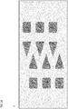
- FIG. 15 shows an 'assist chip' (2), counting 6 semiconductor devices (3), after being transferred to and attached to the carrier substrate (7).
- Two types of semiconductor devices, identified as square or triangle, are present in the 'assist chip' (2).
- the devices (3) are ready to be singulated.
- FIG. 16 shows the result after singulation of the semiconductor devices (3) by removing the frame (4).
- Fig. 17 shows, after further processing, how these devices (3) are connected in pairs to yield a final system, containing 2 different semiconductor devices (3) connected to each-other and having an connection pattern (13) to access these semiconductor devices (3) from outside.
- the connection pattern (13) is formed after the transfer of the 'assist ship '2' and the singulation of the semiconductor devices (3).
- FIG. 18 , FIG. 19 and FIG. 20 illustrate the manufacturing of such a system, for the situation of face-down chip placement.
- FIG. 18 shows the carrier substrate (2) prepared for face-down chip placement.
- the substrate contains the alignment marks (8) and the required metallization pattern for the final system.
- Fig. 19 shows an 'assist chip' (2), counting 6 semiconductor devices (3), after being transferred faced-down and attached to the carrier substrate (7). Two types of semiconductor devices, identified as square or triangle, are present in the 'assist chip' (2).
- the devices (3) are ready to be singulated.
- FIG. 18 shows the carrier substrate (2) prepared for face-down chip placement.
- the substrate contains the alignment marks (8) and the required metallization pattern for the final system.
- Fig. 19 shows an 'assist chip' (2), counting 6 semiconductor devices (3), after being transferred faced-down and attached to the carrier substrate (7).
- Two types of semiconductor devices, identified as square or triangle, are present in the 'assist chip' (2).
- connection pattern (13) is formed after the transfer of the 'assist ship '2' and the singulation of the semiconductor devices (3).
- a rectangular shaped chip (2) comprising multiple semiconductor devices (3) was manufactured on a semiconductor substrate (1).
- the disclosed method for transferring and placing the rectangular shaped chip (2) can also be applied if the 'assist chip' only contains semiconductor device (3) having a shape other than rectangular.
- Such arbitrarily shaped semiconductor device (3) can be transferred and placed using conventional pick-and-place tools. After removing the frame, the singulated semiconductor device (3) remains attached to the carrier substrate (3) and is ready for further processing.
- the carrier substrate (7) was provided with alignment markers (8) for correctly positioning the rectangular shaped chip (2) thereon. If this alignment is less critical then these alignment markers (8) may not be needed.
Landscapes
- Engineering & Computer Science (AREA)
- Manufacturing & Machinery (AREA)
- Microelectronics & Electronic Packaging (AREA)
- Dicing (AREA)
- Container, Conveyance, Adherence, Positioning, Of Wafer (AREA)
Abstract
Description
- The present disclosure relates to methods for placing semiconductor devices, such as Integrated Circuits and/or micro-electromechanical devices (MEMS), on another substrate.
- In particular, this disclosure relates to methods for placing a semiconductor device to another substrate. In particular this disclosure relates to methods for placing one or more arbitrarily shaped semiconductor devices to another substrate.
- Semiconductor devices, such as Integrated Circuits and micro-electromechanical devices (MEMS), are manufactured using semiconductor process technology enabling highly accurate alignment of individual patterns needed to create a semiconductor device. Afterwards, these devices can be transferred to and placed onto another substrate, e.g. for post-processing or for chip packaging. Typically they are placed individually using a pick-and-place tool. Although advanced pick-and-place tools have good alignment capabilities, their accuracy of placing the individual devices is considerably less than the accuracy obtained with state-of-the-art lithographic tools used for fabrication of the semiconductor devices. Consequently, in post-processing or packaging the transferred semiconductor devices, one has to take into account this reduced placement accuracy. Devices transferred to a common substrate may be misaligned towards each-other. In addition, features patterned on a transferred device, during a postprocessing or packaging process, must be sufficiently large to avoid misalignment towards the transferred device. In case narrow patterns on a transferred device are required, device by device processing of such narrow pattern is needed to ensure an acceptable alignment of each narrow pattern to the corresponding transferred device. As parallel processing is not feasible, this will result in a low fabrication speed.
- Pick-and-place tools are designed to handle the transfer of rectangular shaped semiconductor devices, obtained by dicing the semiconductor substrate, used to manufacture these devices, into rectangular chips. Semiconductor devices having an arbitrarily shape can't be diced with conventional dicing tools.
- Hence, there is a need to place arbitrarily shaped chips with improved accuracy and throughput compared to state of the art. Preferably this transfer is executed using conventional post-processing equipment.
- The present disclosure will be described with respect to particular embodiments and with reference to certain drawings but the disclosure is not limited thereto but only by the claims. The drawings described are only schematic and are non-limiting. In the drawings, the size of some of the elements may be exaggerated and not drawn on scale for illustrative purposes. The dimensions and the relative dimensions do not correspond to actual reductions to practice of the disclosure. In the different figures, the same reference signs refer to the same or analogous elements.
-
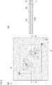
FIG 1a-d illustrate an embodiment of the disclosure, with (a), (b) being top views and (c), (d) being cross-sectional views AA. -
FIG 2a-b illustrate an embodiment of the disclosure, with (a) being a top view and (b) a cross-sectional view AA. -
FIG 3a-b illustrate an embodiment of the disclosure, with (a) being a top view and (b) a cross-sectional view AA. -
FIG 4a-b illustrate an embodiment of the disclosure, with (a) being a top view and (b) a cross-sectional view AA. -
FIG 5a-b illustrate an embodiment of the disclosure, with (a) being a top view and (b) a cross-sectional view AA. -
FIG 6a-b illustrate an embodiment of the disclosure, with (a) being a top view and (b) a cross-sectional view AA. -
FIG 7a-b illustrate an embodiment of the disclosure, with (a) being a top view and (b) a cross-sectional view AA. -
FIG 8a-b illustrate an embodiment of the disclosure, with (a) being a top view and (b) a cross-sectional view AA. -
FIG 9a-b illustrate an embodiment of the disclosure, with (a) being a top view and (b) a cross-sectional view AA. -
FIG 10a-b illustrate an embodiment of the disclosure, with (a) being a top view and (b) a cross-sectional view AA. -
FIG 11a-b illustrate an embodiment of the disclosure, with (a) being a top view and (b) a cross-sectional view AA. -
FIG 12a-b illustrate an embodiment of the disclosure, with (a) being a top view and (b) a cross-sectional view AA. -
FIG 13a-b illustrate an embodiment of the disclosure, with (a) being a top view and (b) a cross-sectional view AA. -
FIG 14a-b illustrate an embodiment of the disclosure, with (a) being a top view and (b) a cross-sectional view AA. -
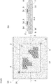
FIG 15 illustrates an embodiment of the disclosure showing multiple semiconductor devices of different type contained in a single assist chip. The assist chip is placed on the substrate using the alignment markers for correct positioning. The semiconductor devices are placed in the face-up direction. -
FIG 16 illustrates an embodiment of the disclosure showing multiple semiconductor devices of different type, previously contained in a single assist chip, after removal of the frame to singulate the individual semiconductor devices. -
FIG 17 illustrates an embodiment of the disclosure showing a system containing post-processed semiconductor devices of two different types, according toFIG 15 , connected to each-other with metal interconnects. -
FIG 18 illustrates an embodiment of the disclosure showing the substrate including metal interconnects, prior to the placement of a multiple semiconductor devices of two different types contained in a single assist chip. -
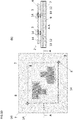
FIG 19 illustrates an embodiment of the disclosure showing the substrate including metal interconnects, after the placement of multiple semiconductor devices of different two type contained in a single assist chip, according toFIG 18 . The semiconductor devices are placed in the face-down direction (i.e. flip chipped). The assist chip is placed on the substrate using the alignment markers for correct positioning, to ensure that the semiconductor devices are contacting the metallization pattern on the substrate at the desired location. -
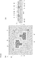
FIG 20 illustrates an embodiment of the disclosure showing multiple semiconductor devices of two different types, previously contained in a single assist chip according toFIG 19 , after removal of the frame to singulate the individual semiconductor devices of different type, which have been placed face-down on the substrate with metal patterns. Further post-processing results in a system containing two semiconductor devices of different type connected to each-other. - In aspect, a method is disclosed for placing on a carrier substrate a semiconductor device, the method comprising: providing a semiconductor substrate comprising a rectangular shaped assist chip which comprises at least one semiconductor device surrounded by a metal-free border, dicing the semiconductor substrate to singulate the rectangular shaped assist chip, providing a carrier substrate having adhesive thereon, transferring to and placing on the carrier substrate the rectangular shaped assist chip, thereby contacting the adhesive with the assist chip at least at the location of the semiconductor device, and; singulating the semiconductor device, while remaining attached to the carrier substrate by the adhesive, by removing the part of rectangular shaped assist chip other than the semiconductor device. This at least one semiconductor device can have a shape other than being rectangular. More than on semiconductor device, of any shape, can be contained by the assist chip. Preferably the carrier substrate contains markers for aligning the assist chip when being placed thereon. On the carrier substrate a support may be formed at each location where a semiconductor device is to be placed and the adhesive is then provided on each support. While the semiconductor device remains attached to the carrier substrate by the adhesive, the semiconductor device can be post-processed.
- In another aspect, a carrier substrate is disclosed comprising at least one rectangular shaped assist chip which comprises a semiconductor device surrounded by a metal-free border, the assist chip being attached by an adhesive to the carrier substrate at least at the location of a semiconductor device. This assist chip can contain multiple semiconductor devices of arbitrary shape. Preferably at least one semiconductor device has a shape other than rectangular.
- In another aspect, a semiconductor substrate is disclosed comprising at least one rectangular shaped assist chip which comprises at least one semiconductor device surrounded by a metal-free border. This assist chip can contain multiple semiconductor devices of arbitrary shape. Preferably at least one semiconductor device has a shape other than rectangular.
- Moreover, the terms top, bottom, over, under and the like in the description and the claims are used for descriptive purposes and not necessarily for describing relative positions. It is to be understood that the terms so used are interchangeable under appropriate circumstances and that the embodiments of the disclosure described herein are capable of operation in other orientations than described or illustrated herein.
- It is to be noticed that the term "comprising", used in the claims, should not be interpreted as being restricted to the means listed thereafter; it does not exclude other elements or steps. It is thus to be interpreted as specifying the presence of the stated features, integers, steps or components as referred to, but does not preclude the presence or addition of one or more other features, integers, steps or components, or groups thereof. Thus, the scope of the expression "a device comprising means A and B" should not be limited to devices consisting only of components A and B. It means that with respect to the present disclosure, the only relevant components of the device are A and B.
- Reference throughout this specification to "one embodiment" or "an embodiment" means that a particular feature, structure or characteristic described in connection with the embodiment is included in at least one embodiment of the present disclosure. Thus, appearances of the phrases "in one embodiment" or "in an embodiment" in various places throughout this specification are not necessarily all referring to the same embodiment, but may. Furthermore, the particular features, structures or characteristics may be combined in any suitable manner, as would be apparent to one of ordinary skill in the art from this disclosure, in one or more embodiments. Similarly it should be appreciated that in the description of exemplary embodiments of the disclosure, various features of the disclosure are sometimes grouped together in a single embodiment, figure, or description thereof for the purpose of streamlining the disclosure and aiding in the understanding of one or more of the various inventive aspects. This method of disclosure, however, is not to be interpreted as reflecting an intention that the claimed disclosure requires more features than are expressly recited in each claim. Rather, as the following claims reflect, inventive aspects lie in less than all features of a single foregoing disclosed embodiment. Thus, the claims following the detailed description are hereby expressly incorporated into this detailed description, with each claim standing on its own as a separate embodiment of this disclosure.
- Furthermore, while some embodiments described herein include some but not other features included in other embodiments, combinations of features of different embodiments are meant to be within the scope of the disclosure, and form different embodiments, as would be understood by those in the art. For example, in the following claims, any of the claimed embodiments can be used in any combination.
- In the description with chip is meant a piece of semiconductor material, in and/or on which structures can be defined using semiconductor process technology. With semiconductor device is meant the combination of patterned and un-patterned layers forming a functional structure. Semiconductor process technology refers to the state-of-art technology of integrated processing whereby layers are formed on a semiconductor substrate to form a semiconductor device. Post-processing refers to the processing of semiconductor devices after they have been formed using semiconductor technology processing. Post-processing is done on the diced chip containing the semiconductor device. Post-processing may refer to packaging the diced chip or to forming additional patterned and un-patterned layers on the diced chips, optionally connecting diced chips.
- A method is disclosed for transferring to and placing on a substrate a semiconductor device thereby maintaining the alignment accuracy of conventional semiconductor tools used to manufacture these semiconductor devices. Thanks to this alignment accurancy, during post-processing, simultaneously lithographic patterning of the transferred semiconductor devices is possible, with even increased accuracy over state-of-the-art technology. Moreover, this method is not limited to rectangular shaped semiconductor devices, but enables transfer, placing and further processing on semiconductor devices having a random shape. This method enables more then one semiconductor device to be transferred in parallel to a substrate.
- On a semiconductor substrate (1), within the boundary of a rectangular shaped chip (2), multiple semiconductor devices (3) are formed in parallel using conventional semiconductor processing.
- These semiconductor devices (3) can be Integrated Circuits, micro-electromechanical devices (MEMS) or a combination thereof. For Integrated Circuits active and/or passive components are created in the so-called Front-End-Of-Line, whereby these components are electrically connected in the so-called Back-End-Of-Line formed thereupon. The smaller semiconductor devices (3) are positioned relatively to each-other on the predetermined position they need to have on the common substrate to which they (3) will be transferred to and placed on after dicing. The semiconductor devices (3) are hence in a fixed positional relationship towards each-other. These semiconductor devices (3) may be rectangular in shape, but can have any arbitrary shape. Each semiconductor device (3) is surrounded by a, preferably small, metal-free border (6) outlining the semiconductor device (3), as indicated in
FIG. 1a-b by the dotted line. As will be disclosed in subsequent paragraphs, the absence of metal in the border (6) easies removal of the material present in this border (6) when separating the multiple semiconductor devices (3) after transfer thereof. During the semiconductor processing of the substrate (1), care must be taken to avoid the presence of metal in this border (6). Typically, this border (6) has a width in the range of 100 to 300 micrometer (um). Although inFIG. 1a-c , the 'assist chip' (2) only contains two semiconductor devices (3), the disclosure is not limited thereto. - The rectangular shaped chip (2) is referred to as 'assist chip'. As can be seen in
FIG. 1a-b , only part of the area of the 'assist chip' (2) will be taken up by the semiconductor devices (3). The remaining area of the 'assist chip' (2) outside the border (6) is referred to as 'semiconductor frame' (4). Within this frame (4) additional patterns (not shown), such as dummy patterns, can be present as may be necessitated for correct semiconductor processing of the semiconductor devices (3). Also test structures and/or alignment patterns may be present in the frame (4). Preferably the area of the 'semiconductor frame' (4) should be as small as possible to increase the yield of the semiconductor processing. The minimal spacing between the semiconductor devices (3) is inter alia also determined by the area needed to package the semiconductor devices (3). As seen inFIG. 1a , the semiconductor substrate (1) contains a pattern of rectangular shaped chips (2) separated by conventional scribe lines (5). The semiconductor substrate (1) will be diced into individual chips (2) along these scribe lines (5), whereby each chip (2) corresponds to an 'assist chip' (2) comprising multiple semiconductor devices (3). Optionally, as illustrated by the cross-section A-A of byFIG. 1 (c) , the material (15), typically Back-End-Of-Line material, in the border (6) is removed down to the semiconductor substrate (2) thereby forming corresponding trenches surrounding each semiconductor device (3). This removal can be done using conventional lithographic patterning of the border (6). If no metal patterns are included in the frame (4), e.g. if the semiconductor devices (3) are MEMS devices, then all material in the frame (4) on top of the semiconductor substrate (1) can be removed as illustrated by the cross-section A-A ofFIG. 1 (d) . - The semiconductor substrate (2) is now ready to be diced. Using conventional dicing processes, each rectangular 'assist chip' (2) is singulated. Optionally the semiconductor substrate (1) can be further thinned, e.g. by grinding, to reduce the overall thickness of the diced chip.
- A carrier substrate (7) is provided to which a singulated 'assist chip' (2) can be transferred to and placed upon using conventional pick-and-place tools. Preferably, on this carrier substrate (7) alignment marks (8) are provided allowing accurate positioning of the 'assist chip' (2), as illustrated in
FIG. 2a . Typically these alignment markers (8) are formed in an optically visible layer (9) present on the substrate (7). The dotted lines inFIG. 2a indicates the position of the 'assist chip' (2). The dot-point lines inFIG. 2a and the semiconductor devices (3) when placed on the carrier substrate (7). - The 'assist chip' can be fixed, e.g. face-up, directly on the carrier substrate (7) by providing adhesive (10) on the carrier substrate (7). If this adhesive is only provided at locations corresponding to the position of the semiconductor devices (3) when being placed on the carrier substrate (7), then these alignment markers (8) may be required to accuraterely align the 'assist chip' (2), and hence the semiconductor devices (3), to the locations containing the adhesive (10). As shown in
FIG. 3a , this adhesive (10) is applied within the dash-dotted lines indicating the future location of the semiconductor devices (3). Restricting the adhesive to these locations, may be necessitated by the fact that the adhesive (10) is difficult to remove from the carrier substrate (7), in parrticular after curing of the adhesive, or the adhesive may not be exposed to further processing after placing the 'assist chip' (2). Otherwise, the adhesive can be applied over a sufficiently large area in which the 'assist chip' (2) can be placed thereby adhering to the carrier substrate (7). Depending on the required alignment accuracy, alignment markers (8) may still be needed, even if the whole of the 'assist chip' (2) is adhered to the carrier substrate (7). - Alternatively, a support layer (11) (not shown) is formed on the carrier substrate (7). This support layer (11) is patterned to form a support (12) at locations corresponding to the position of the semiconductor devices (3) when placed in face-up direction on the carrier substrate (7). As illustrated in
FIG. 4a this support preferably extends beyond the footprint of the semiconductor devices (3) indicated by the dot-point lines. Thanks to this extension, some misalignment of the 'assist chip' (2) when being placed on the carrier substrate (7), can be tolerated. Optionally the alignment marks (8) can be patterned in the support layer (11) as well, in which case layer (9) may become obsolete. On the supports (12) adhesive (10) is applied, either as dots as shown inFIG. 4a-b , or uniform over the surface of the support (12). - An advantage of the method disclosed is that even for thinned 'assist chips' (2), e.g. less than 100 micrometer, typcially less than 50 micrometer, excess adhesive may stay underneath the 'assist chip' (2) when applied locally. Even if such excess adhesive would extend above the height of the 'assist chip' (2) when placed on the carier substrate (7), appropriate dimension of the 'assist chip' (2), i.e. providing sufficient margin between the border of the 'assist chip' (2) and the border (6) surrounding the semiconductor device (3) will prevent the adhesive (10) from reaching the semiconductor device (3).
- It is also possible to place to assist chip (2) faced-down, hence with the metal bondpads facing towards the carrier substrate (7). In this case, the substrate (7) should carry the suitable metallization patterns prior to chip placement, to ensure that the correct electrical interconnections are realized between a metal bondpad of a device (3) and the metallization pattern . The placement can be done by using i.e. flip-chip technology, to realize a conductive connection between the metallization pattern and the bondpads of the semiconductor devices (3), while good adhesion is realized between the semiconductor devices (3) and the carrier substrate (7). This is further illustrated by
FIG 18 ,19 and20 . - To the carrier substrate (7), the singulated 'assist chip' (2) is transferred and placed upon, thereby making physical contact with the adhesive (10). Thanks to the alignment markers (8) present, the 'assist chip' (2) can be accurately positioned on the carrier substrate (7) ensuring the desired position of the semiconductor devices (3) towards the carrier substrate (7) while maintaining their relative position. Thanks to the rectangular shape of the 'assist chip', conventional pick-and-place tools can easily be used for this transfer, alignment and placement.
FIG. 5a-b illustrate the embodiment where the adhesive (10) is applied directly to the carrier substrate (7). -
FIG. 6a-b illustrate the embodiment whereby a support (12) is present on the carrier substrate (7) prior to applying the adhesive (10). After placing the 'assist chip' (2), the adhesive (10) is cured to ensure adhesion between the semiconductor substrate (1) and the carrier substrate (7) at the location of the semiconductor devices (3). - Once the semiconductor devices (3) are adhered to the carrier substrate (7) by the adhesive (10), these semiconductor devices (3) can also be singulated. A photoresist layer (14) is applied over the carrier substrate (7) as shown in
FIG. 7a-b andFIG. 8a-b . Due the spacing between the 'assist chip' (2) and the carrier substrate (7) resist may flow underneath the 'assist chip' (2). This photoresist layer (14) is then patterned to remain on the location of the semiconductor devices (3) while the frame (4) is uncovered. Traces of photoresist may remain underneath the 'assist chip' (2), at least near the edge thereof. The pattern of the photoresist layer (3) may extend over the border of the semiconductor device (3) to ensure that the semiconductor device (3) remains protected. -
FIG. 7a-b andFIG. 9a-b illustrate the embodiment where the adhesive (10) is applied directly to the carrier substrate (7). The photoresist layer (14) is patterned whereby traces of photoresist remain underneath the 'assist chip' (3). -
FIG. 8a-b andFIG. 10a-b illustrate the embodiment whereby a support (12) is present on the carrier substrate (7) prior to applying the adhesive (10). The photoresist layer (14) is patterned whereby traces of photoresist remain underneath the 'assist chip' (3). - As the semiconductor devices (3) are protected by the patterned photoresist layer (14), the frame (4) can be removed, preferably if no metal is present. After removal of the frame (4), the photoresist (14) on the semiconductor devices (3), and if present on the carrier substrate (7) is removed. Attached to and aligned to carrier substrate (7), the semiconductor devices (3) remain in their relative position as defined during the processing of the semiconductor substrate (1). In
FIG. 1(c) and (d) it was shown that either the metal-free border (c) or the metal-free border (d) was removed down to the level of the semiconductor substrate (1). This removal process can be executed on wafer level and is more efficient. After placing the diced chip (2) on the carrier substrate (7), only the semiconductor substrate part of the frame (4) is to be removed to singulate the semiconductor devices (3). -
FIG. 11a-b illustrate the embodiment where the adhesive (10) is applied directly to the carrier substrate (7). -
FIG. 12a-b illustrate the embodiment whereby a support (12) is present on the carrier substrate (7) prior to applying the adhesive (10). - Instead of singulating the semiconductor devices (3) by removing the complete frame (4), preferably only the metal-free border (6) can be removed. A photoresist layer (14) is applied over the carrier substrate (7) as shown in
FIG. 13a-b andFIG. 14a-b . Due the spacing between the 'assist chip' (2) and the carrier substrate (7) resist may flow underneath the 'assist chip' (2). This photoresist layer (14) is then patterned to remain outside the area of the border (6) thereby creating trenches (6) in the photoresist layer (14) surrounding the semiconductor devices (3). Traces of photoresist may remain underneath the 'assist chip' (2), at least near the edge thereof. The pattern of the photoresist layer (3) may extend over the border of the semiconductor device (3) to ensure that the semiconductor device (3) remains protected. Then the material of the border (6) is etched. The part of the frame (4) covered by the photoresist pattern (14) remains. After the etch step, the photoresist on top of the semiconductor devices (3) and of the remaining frame (4) is removed, thereby exposing the remaining part of the frame (4). When removing the traces of the photoresist (14) that were present underneath the 'assist chip' (2), this remainder of the frame (4) will be lifted-off from the carrier substrate (7). This again results in the configuration illustrated byFIG. 11a-b andFIG 12a-b , as the semiconductor devices (3) remain attached by the adhesive (10) during this photoresist (14) removal process. Attached to and aligned to carrier substrate (7), the semiconductor devices (3) remain in their relative position as defined during the processing of the semiconductor substrate (1). - The semiconductor devices (3) can now be further processed, as they remain in their relative position as defined accurately during the processing of the semiconductor substrate (1), while being attached and accurately aligned to carrier substrate (7). This allows post-processing of these semiconductor devices (3), even when small patterns are to be formed upon these semiconductor devices (3), e.g. when parts of the semiconductor devices (3) need to be connected with each-other or with other devices present on or to be formed on the carrier substrate (7).
- In the figures
FIG. 1 to 14 used to illustrate the methods of this disclosure, the semiconductor devices (3) were of equal shape and size. This is not a requirement. As already indicated above, the methods according this disclosure, allow any shape and size of the semiconductor devices (3) contained within the boundary of the 'assist chip' (2). Within one 'assist chip' (2) one can design multiple semiconductor devices (3), each having a different layout, shape and size. After transferring and singulating these semiconductor devices (3), as disclosed above, one can create any desired connection between singulated semiconductor devices (3). This may result, after packaging, in a single system containing multiple arbitrarily shaped semiconductor devices, accurately aligned to each-other with the desired, small size, interconnect pattern. -
FIG. 15 ,FIG. 16 andFIG. 17 illustrate the manufacturing of such a system, for the situation of face-up chip placement.FIG. 15 shows an 'assist chip' (2), counting 6 semiconductor devices (3), after being transferred to and attached to the carrier substrate (7). Two types of semiconductor devices, identified as square or triangle, are present in the 'assist chip' (2). The devices (3) are ready to be singulated.FIG. 16 shows the result after singulation of the semiconductor devices (3) by removing the frame (4).Fig. 17 shows, after further processing, how these devices (3) are connected in pairs to yield a final system, containing 2 different semiconductor devices (3) connected to each-other and having an connection pattern (13) to access these semiconductor devices (3) from outside. Here the connection pattern (13) is formed after the transfer of the 'assist ship '2' and the singulation of the semiconductor devices (3). -
FIG. 18 ,FIG. 19 andFIG. 20 illustrate the manufacturing of such a system, for the situation of face-down chip placement.FIG. 18 shows the carrier substrate (2) prepared for face-down chip placement. The substrate contains the alignment marks (8) and the required metallization pattern for the final system.Fig. 19 shows an 'assist chip' (2), counting 6 semiconductor devices (3), after being transferred faced-down and attached to the carrier substrate (7). Two types of semiconductor devices, identified as square or triangle, are present in the 'assist chip' (2). The devices (3) are ready to be singulated.FIG. 20 shows the result after singulation of the semiconductor devices (3) by removing the frame (4), and after further processing to define the final system, containing 2 different semiconductor devices (3) connected to each-other and having an connection pattern to access these semiconductor devices (3) from outside. Here the connection pattern (13) is formed after the transfer of the 'assist ship '2' and the singulation of the semiconductor devices (3). - In the foregoing paragraphs, a rectangular shaped chip (2) comprising multiple semiconductor devices (3) was manufactured on a semiconductor substrate (1). The disclosed method for transferring and placing the rectangular shaped chip (2) can also be applied if the 'assist chip' only contains semiconductor device (3) having a shape other than rectangular. Such arbitrarily shaped semiconductor device (3) can be transferred and placed using conventional pick-and-place tools. After removing the frame, the singulated semiconductor device (3) remains attached to the carrier substrate (3) and is ready for further processing.
- In the foregoing paragraphs, the carrier substrate (7) was provided with alignment markers (8) for correctly positioning the rectangular shaped chip (2) thereon. If this alignment is less critical then these alignment markers (8) may not be needed.
Claims (12)
- A method for placing on a carrier substrate (7) a semiconductor device (3), the method comprising:- providing a semiconductor substrate (1) comprising a rectangular shaped assist chip (2) which comprises at least one semiconductor device (3) surrounded by a metal-free border (6),- dicing the semiconductor substrate (1) to singulate the rectangular shaped assist chip (2),- providing a carrier substrate (7) having adhesive (10) thereon,- transferring to and placing on the carrier substrate (7) the rectangular shaped assist chip (2), thereby contacting the adhesive with the assist chip (2) at least at the location of the semiconductor device (3), and;- singulating the semiconductor device (3), while remaining attached to the carrier substrate (7) by the adhesive (10), by removing the part of rectangular shaped assist chip (2) other than the semiconductor device (3).
- The method of claim 1, whereby:- at least one semiconductor device (3) has a shape other than rectangular .
- The method of any of the foregoing claims, wherein:- the assist chip (2) contains multiple semiconductor devices (3).
- The method of any of the foregoing claims, wherein:- the carrier substrate (7) contains markers (8) for aligning the assist chip (2) when being placed thereon.
- The method of any of the foregoing claims , further comprising:- forming on the carrier substrate (7) at each location where a semiconductor device (3) is to be placed a support (12),whereby,- the adhesive (10) is provided on each support (12).
- The method of any of the foregoing claims, further comprising:- post-processing the semiconductor device (3) while remaining attached to the carrier substrate (7) by the adhesive (10).
- A carrier substrate (7) comprising at least one rectangular shaped assist chip (2) which comprises a semiconductor device (3) surrounded by a metal-free border (6), the assist chip (2) being attached by an adhesive at to the carrier substrate (7) at least at the location of a semiconductor device (3).
- The carrier substrate (7) of claim 7, wherein the assist chip (2) contains multiple semiconductor devices (3).
- The carrier substrate (7) of claim 7 or 8, wherein at least one semiconductor device (3) has a shape other than rectangular.
- A semiconductor substrate (1) comprising at least one rectangular shaped assist chip (2) which comprises at least one semiconductor device (3) surrounded by a metal-free border (6).
- The semiconductor substrate (1) of claim 10, wherein the assist chip (2) contains multiple semiconductor devices (3).
- The semiconductor substrate (1) of claim 10 or 11, wherein at least one semiconductor device (3) has a shape other than rectangular.
Applications Claiming Priority (1)
| Application Number | Priority Date | Filing Date | Title |
|---|---|---|---|
| EP16202839 | 2016-12-08 |
Publications (2)
| Publication Number | Publication Date |
|---|---|
| EP3333883A1 true EP3333883A1 (en) | 2018-06-13 |
| EP3333883B1 EP3333883B1 (en) | 2025-04-16 |
Family
ID=57539074
Family Applications (1)
| Application Number | Title | Priority Date | Filing Date |
|---|---|---|---|
| EP17204936.3A Active EP3333883B1 (en) | 2016-12-08 | 2017-12-01 | A method for transferring and placing a semiconductor device on a substrate |
Country Status (2)
| Country | Link |
|---|---|
| US (1) | US10910342B2 (en) |
| EP (1) | EP3333883B1 (en) |
Families Citing this family (3)
| Publication number | Priority date | Publication date | Assignee | Title |
|---|---|---|---|---|
| US10529593B2 (en) * | 2018-04-27 | 2020-01-07 | Taiwan Semiconductor Manufacturing Co., Ltd. | Semiconductor package comprising molding compound having extended portion and manufacturing method of semiconductor package |
| DE102019004261A1 (en) * | 2019-06-18 | 2020-12-24 | lnfineon Technologies AG | Method for processing a substrate arrangement and composite wafer structure |
| US12394648B2 (en) * | 2021-03-02 | 2025-08-19 | Samsung Electronics Co., Ltd. | Display transfer structure including light emitting elements and transferring method of light emitting elements |
Citations (5)
| Publication number | Priority date | Publication date | Assignee | Title |
|---|---|---|---|---|
| JPH04192430A (en) * | 1990-11-26 | 1992-07-10 | Mitsubishi Electric Corp | Die bonding method |
| US20070216038A1 (en) * | 2006-03-17 | 2007-09-20 | Park Soo G | Method for producing semiconductor components |
| US20100230799A1 (en) * | 2009-03-13 | 2010-09-16 | Infineon Technologies Ag | Semiconductor device |
| US20110241190A1 (en) * | 2010-03-31 | 2011-10-06 | Klaus Elian | Semiconductor Package |
| US20150221569A1 (en) * | 2014-02-04 | 2015-08-06 | Infineon Technologies Ag | Chip assembling on adhesion layer or dielectric layer, extending beyond chip, on substrate |
Family Cites Families (5)
| Publication number | Priority date | Publication date | Assignee | Title |
|---|---|---|---|---|
| JPH097975A (en) * | 1995-06-22 | 1997-01-10 | Hitachi Ltd | Semiconductor device and manufacturing method thereof |
| JP2001148358A (en) * | 1999-11-19 | 2001-05-29 | Disco Abrasive Syst Ltd | Semiconductor wafer and method for dividing semiconductor wafer |
| US6573156B1 (en) * | 2001-12-13 | 2003-06-03 | Omm, Inc. | Low defect method for die singulation and for structural support for handling thin film devices |
| US9165833B2 (en) * | 2010-01-18 | 2015-10-20 | Semiconductor Components Industries, Llc | Method of forming a semiconductor die |
| US9034734B2 (en) * | 2013-02-04 | 2015-05-19 | Avago Technologies General Ip (Singapore) Pte. Ltd. | Systems and methods for plasma etching compound semiconductor (CS) dies and passively aligning the dies |
-
2017
- 2017-12-01 EP EP17204936.3A patent/EP3333883B1/en active Active
- 2017-12-08 US US15/836,634 patent/US10910342B2/en active Active
Patent Citations (5)
| Publication number | Priority date | Publication date | Assignee | Title |
|---|---|---|---|---|
| JPH04192430A (en) * | 1990-11-26 | 1992-07-10 | Mitsubishi Electric Corp | Die bonding method |
| US20070216038A1 (en) * | 2006-03-17 | 2007-09-20 | Park Soo G | Method for producing semiconductor components |
| US20100230799A1 (en) * | 2009-03-13 | 2010-09-16 | Infineon Technologies Ag | Semiconductor device |
| US20110241190A1 (en) * | 2010-03-31 | 2011-10-06 | Klaus Elian | Semiconductor Package |
| US20150221569A1 (en) * | 2014-02-04 | 2015-08-06 | Infineon Technologies Ag | Chip assembling on adhesion layer or dielectric layer, extending beyond chip, on substrate |
Also Published As
| Publication number | Publication date |
|---|---|
| US20180166416A1 (en) | 2018-06-14 |
| US10910342B2 (en) | 2021-02-02 |
| EP3333883B1 (en) | 2025-04-16 |
Similar Documents
| Publication | Publication Date | Title |
|---|---|---|
| US10354934B2 (en) | Semiconductor packages and methods of packaging semiconductor devices | |
| US9978655B2 (en) | Semiconductor device and method of adaptive patterning for panelized packaging with dynamic via clipping | |
| KR101901988B1 (en) | Method of manufacturing semiconductor package | |
| US9165890B2 (en) | Chip package comprising alignment mark and method for forming the same | |
| US11049816B2 (en) | Alignment mark and semiconductor device, and fabrication methods thereof | |
| US9530680B2 (en) | Method of fabricating semiconductor package, semiconductor chip supporting carrier and chip mounting device | |
| US10553489B2 (en) | Partitioned wafer and semiconductor die | |
| US10438881B2 (en) | Packaging arrangements including high density interconnect bridge | |
| EP3333883B1 (en) | A method for transferring and placing a semiconductor device on a substrate | |
| US9548248B2 (en) | Method of processing a substrate and a method of processing a wafer | |
| US20190109092A1 (en) | Positioning structure having positioning unit | |
| CN113257692B (en) | A method for manufacturing a semiconductor packaging structure and a semiconductor packaging structure | |
| US10770432B2 (en) | ASICS face to face self assembly | |
| US9324686B2 (en) | Semiconductor chips having improved solidity, semiconductor packages including the same and methods of fabricating the same | |
| US10304716B1 (en) | Package structure and manufacturing method thereof | |
| US20190194014A1 (en) | Pressure sensor structure configured for wafer-level calibration | |
| US7592236B2 (en) | Method for applying a structure of joining material to the back surfaces of semiconductor chips | |
| CN111048459B (en) | Method for aligning wafer, method for bonding wafer and device for aligning wafer | |
| TWI473189B (en) | Method for wafer-level testing diced multi-dice stacked packages | |
| US20080160670A1 (en) | Physical alignment features on integrated circuit devices for accurate die-in-substrate embedding | |
| KR20150093878A (en) | Semiconductor package and manufacturing method thereof | |
| US20200211888A1 (en) | Patterned carrier wafers and methods of making and using the same | |
| HK1234252B (en) | Semiconductor device and method of adaptive patterning for panelized packaging with dynamic via clipping |
Legal Events
| Date | Code | Title | Description |
|---|---|---|---|
| PUAI | Public reference made under article 153(3) epc to a published international application that has entered the european phase |
Free format text: ORIGINAL CODE: 0009012 |
|
| STAA | Information on the status of an ep patent application or granted ep patent |
Free format text: STATUS: THE APPLICATION HAS BEEN PUBLISHED |
|
| AK | Designated contracting states |
Kind code of ref document: A1 Designated state(s): AL AT BE BG CH CY CZ DE DK EE ES FI FR GB GR HR HU IE IS IT LI LT LU LV MC MK MT NL NO PL PT RO RS SE SI SK SM TR |
|
| AX | Request for extension of the european patent |
Extension state: BA ME |
|
| STAA | Information on the status of an ep patent application or granted ep patent |
Free format text: STATUS: REQUEST FOR EXAMINATION WAS MADE |
|
| 17P | Request for examination filed |
Effective date: 20181211 |
|
| RBV | Designated contracting states (corrected) |
Designated state(s): AL AT BE BG CH CY CZ DE DK EE ES FI FR GB GR HR HU IE IS IT LI LT LU LV MC MK MT NL NO PL PT RO RS SE SI SK SM TR |
|
| STAA | Information on the status of an ep patent application or granted ep patent |
Free format text: STATUS: EXAMINATION IS IN PROGRESS |
|
| 17Q | First examination report despatched |
Effective date: 20210707 |
|
| RAP3 | Party data changed (applicant data changed or rights of an application transferred) |
Owner name: UNIVERSITEIT GENT Owner name: IMEC VZW |
|
| GRAP | Despatch of communication of intention to grant a patent |
Free format text: ORIGINAL CODE: EPIDOSNIGR1 |
|
| STAA | Information on the status of an ep patent application or granted ep patent |
Free format text: STATUS: GRANT OF PATENT IS INTENDED |
|
| RIC1 | Information provided on ipc code assigned before grant |
Ipc: H01L 25/065 20060101ALN20250127BHEP Ipc: H01L 23/544 20060101ALN20250127BHEP Ipc: H01L 21/78 20060101ALN20250127BHEP Ipc: H01L 21/67 20060101ALI20250127BHEP Ipc: H10D 62/10 20250101ALI20250127BHEP Ipc: H01L 25/00 20060101ALI20250127BHEP Ipc: H01L 21/58 20060101ALI20250127BHEP Ipc: H01L 21/60 20060101AFI20250127BHEP |
|
| GRAS | Grant fee paid |
Free format text: ORIGINAL CODE: EPIDOSNIGR3 |
|
| INTG | Intention to grant announced |
Effective date: 20250210 |
|
| RIN1 | Information on inventor provided before grant (corrected) |
Inventor name: VANDECASTEELE, BJORN Inventor name: OP DE BEECK, MARIA |
|
| GRAA | (expected) grant |
Free format text: ORIGINAL CODE: 0009210 |
|
| STAA | Information on the status of an ep patent application or granted ep patent |
Free format text: STATUS: THE PATENT HAS BEEN GRANTED |
|
| AK | Designated contracting states |
Kind code of ref document: B1 Designated state(s): AL AT BE BG CH CY CZ DE DK EE ES FI FR GB GR HR HU IE IS IT LI LT LU LV MC MK MT NL NO PL PT RO RS SE SI SK SM TR |
|
| REG | Reference to a national code |
Ref country code: GB Ref legal event code: FG4D |
|
| REG | Reference to a national code |
Ref country code: CH Ref legal event code: EP Ref country code: DE Ref legal event code: R096 Ref document number: 602017088919 Country of ref document: DE |
|
| P01 | Opt-out of the competence of the unified patent court (upc) registered |
Free format text: CASE NUMBER: APP_14881/2025 Effective date: 20250327 |
|
| REG | Reference to a national code |
Ref country code: IE Ref legal event code: FG4D |
|
| REG | Reference to a national code |
Ref country code: NL Ref legal event code: MP Effective date: 20250416 |
|
| PG25 | Lapsed in a contracting state [announced via postgrant information from national office to epo] |
Ref country code: NL Free format text: LAPSE BECAUSE OF FAILURE TO SUBMIT A TRANSLATION OF THE DESCRIPTION OR TO PAY THE FEE WITHIN THE PRESCRIBED TIME-LIMIT Effective date: 20250416 |
|
| REG | Reference to a national code |
Ref country code: AT Ref legal event code: MK05 Ref document number: 1786388 Country of ref document: AT Kind code of ref document: T Effective date: 20250416 |
|
| PG25 | Lapsed in a contracting state [announced via postgrant information from national office to epo] |
Ref country code: PT Free format text: LAPSE BECAUSE OF FAILURE TO SUBMIT A TRANSLATION OF THE DESCRIPTION OR TO PAY THE FEE WITHIN THE PRESCRIBED TIME-LIMIT Effective date: 20250818 Ref country code: FI Free format text: LAPSE BECAUSE OF FAILURE TO SUBMIT A TRANSLATION OF THE DESCRIPTION OR TO PAY THE FEE WITHIN THE PRESCRIBED TIME-LIMIT Effective date: 20250416 Ref country code: ES Free format text: LAPSE BECAUSE OF FAILURE TO SUBMIT A TRANSLATION OF THE DESCRIPTION OR TO PAY THE FEE WITHIN THE PRESCRIBED TIME-LIMIT Effective date: 20250416 |
|
| REG | Reference to a national code |
Ref country code: LT Ref legal event code: MG9D |
|
| PG25 | Lapsed in a contracting state [announced via postgrant information from national office to epo] |
Ref country code: NO Free format text: LAPSE BECAUSE OF FAILURE TO SUBMIT A TRANSLATION OF THE DESCRIPTION OR TO PAY THE FEE WITHIN THE PRESCRIBED TIME-LIMIT Effective date: 20250716 Ref country code: GR Free format text: LAPSE BECAUSE OF FAILURE TO SUBMIT A TRANSLATION OF THE DESCRIPTION OR TO PAY THE FEE WITHIN THE PRESCRIBED TIME-LIMIT Effective date: 20250717 |
|
| PG25 | Lapsed in a contracting state [announced via postgrant information from national office to epo] |
Ref country code: PL Free format text: LAPSE BECAUSE OF FAILURE TO SUBMIT A TRANSLATION OF THE DESCRIPTION OR TO PAY THE FEE WITHIN THE PRESCRIBED TIME-LIMIT Effective date: 20250416 |
|
| PG25 | Lapsed in a contracting state [announced via postgrant information from national office to epo] |
Ref country code: BG Free format text: LAPSE BECAUSE OF FAILURE TO SUBMIT A TRANSLATION OF THE DESCRIPTION OR TO PAY THE FEE WITHIN THE PRESCRIBED TIME-LIMIT Effective date: 20250416 |
|
| PG25 | Lapsed in a contracting state [announced via postgrant information from national office to epo] |
Ref country code: HR Free format text: LAPSE BECAUSE OF FAILURE TO SUBMIT A TRANSLATION OF THE DESCRIPTION OR TO PAY THE FEE WITHIN THE PRESCRIBED TIME-LIMIT Effective date: 20250416 |
|
| PG25 | Lapsed in a contracting state [announced via postgrant information from national office to epo] |
Ref country code: AT Free format text: LAPSE BECAUSE OF FAILURE TO SUBMIT A TRANSLATION OF THE DESCRIPTION OR TO PAY THE FEE WITHIN THE PRESCRIBED TIME-LIMIT Effective date: 20250416 |
|
| PG25 | Lapsed in a contracting state [announced via postgrant information from national office to epo] |
Ref country code: RS Free format text: LAPSE BECAUSE OF FAILURE TO SUBMIT A TRANSLATION OF THE DESCRIPTION OR TO PAY THE FEE WITHIN THE PRESCRIBED TIME-LIMIT Effective date: 20250716 |
|
| PG25 | Lapsed in a contracting state [announced via postgrant information from national office to epo] |
Ref country code: IS Free format text: LAPSE BECAUSE OF FAILURE TO SUBMIT A TRANSLATION OF THE DESCRIPTION OR TO PAY THE FEE WITHIN THE PRESCRIBED TIME-LIMIT Effective date: 20250816 |
|
| PG25 | Lapsed in a contracting state [announced via postgrant information from national office to epo] |
Ref country code: LV Free format text: LAPSE BECAUSE OF FAILURE TO SUBMIT A TRANSLATION OF THE DESCRIPTION OR TO PAY THE FEE WITHIN THE PRESCRIBED TIME-LIMIT Effective date: 20250416 |
|
| REG | Reference to a national code |
Ref country code: DE Ref legal event code: R079 Ref document number: 602017088919 Country of ref document: DE Free format text: PREVIOUS MAIN CLASS: H01L0021600000 Ipc: H10W0070010000 |
|
| PGFP | Annual fee paid to national office [announced via postgrant information from national office to epo] |
Ref country code: DE Payment date: 20251126 Year of fee payment: 9 |
|
| PG25 | Lapsed in a contracting state [announced via postgrant information from national office to epo] |
Ref country code: SM Free format text: LAPSE BECAUSE OF FAILURE TO SUBMIT A TRANSLATION OF THE DESCRIPTION OR TO PAY THE FEE WITHIN THE PRESCRIBED TIME-LIMIT Effective date: 20250416 Ref country code: DK Free format text: LAPSE BECAUSE OF FAILURE TO SUBMIT A TRANSLATION OF THE DESCRIPTION OR TO PAY THE FEE WITHIN THE PRESCRIBED TIME-LIMIT Effective date: 20250416 |
|
| REG | Reference to a national code |
Ref country code: DE Ref legal event code: R097 Ref document number: 602017088919 Country of ref document: DE |
|
| PG25 | Lapsed in a contracting state [announced via postgrant information from national office to epo] |
Ref country code: CZ Free format text: LAPSE BECAUSE OF FAILURE TO SUBMIT A TRANSLATION OF THE DESCRIPTION OR TO PAY THE FEE WITHIN THE PRESCRIBED TIME-LIMIT Effective date: 20250416 |
|
| PG25 | Lapsed in a contracting state [announced via postgrant information from national office to epo] |
Ref country code: EE Free format text: LAPSE BECAUSE OF FAILURE TO SUBMIT A TRANSLATION OF THE DESCRIPTION OR TO PAY THE FEE WITHIN THE PRESCRIBED TIME-LIMIT Effective date: 20250416 |
|
| PG25 | Lapsed in a contracting state [announced via postgrant information from national office to epo] |
Ref country code: SK Free format text: LAPSE BECAUSE OF FAILURE TO SUBMIT A TRANSLATION OF THE DESCRIPTION OR TO PAY THE FEE WITHIN THE PRESCRIBED TIME-LIMIT Effective date: 20250416 Ref country code: RO Free format text: LAPSE BECAUSE OF FAILURE TO SUBMIT A TRANSLATION OF THE DESCRIPTION OR TO PAY THE FEE WITHIN THE PRESCRIBED TIME-LIMIT Effective date: 20250416 |
|
| PG25 | Lapsed in a contracting state [announced via postgrant information from national office to epo] |
Ref country code: IT Free format text: LAPSE BECAUSE OF FAILURE TO SUBMIT A TRANSLATION OF THE DESCRIPTION OR TO PAY THE FEE WITHIN THE PRESCRIBED TIME-LIMIT Effective date: 20250416 |
|
| PLBE | No opposition filed within time limit |
Free format text: ORIGINAL CODE: 0009261 |
|
| STAA | Information on the status of an ep patent application or granted ep patent |
Free format text: STATUS: NO OPPOSITION FILED WITHIN TIME LIMIT |
|
| REG | Reference to a national code |
Ref country code: CH Ref legal event code: L10 Free format text: ST27 STATUS EVENT CODE: U-0-0-L10-L00 (AS PROVIDED BY THE NATIONAL OFFICE) Effective date: 20260225 |
|
| 26N | No opposition filed |
Effective date: 20260119 |
|
| PG25 | Lapsed in a contracting state [announced via postgrant information from national office to epo] |
Ref country code: LT Free format text: LAPSE BECAUSE OF FAILURE TO SUBMIT A TRANSLATION OF THE DESCRIPTION OR TO PAY THE FEE WITHIN THE PRESCRIBED TIME-LIMIT Effective date: 20250416 |
|
| PG25 | Lapsed in a contracting state [announced via postgrant information from national office to epo] |
Ref country code: MC Free format text: LAPSE BECAUSE OF FAILURE TO SUBMIT A TRANSLATION OF THE DESCRIPTION OR TO PAY THE FEE WITHIN THE PRESCRIBED TIME-LIMIT Effective date: 20250416 |
|
| REG | Reference to a national code |
Ref country code: CH Ref legal event code: H13 Free format text: ST27 STATUS EVENT CODE: U-0-0-H10-H13 (AS PROVIDED BY THE NATIONAL OFFICE) Effective date: 20260723 |
|
| PG25 | Lapsed in a contracting state [announced via postgrant information from national office to epo] |
Ref country code: SE Free format text: LAPSE BECAUSE OF FAILURE TO SUBMIT A TRANSLATION OF THE DESCRIPTION OR TO PAY THE FEE WITHIN THE PRESCRIBED TIME-LIMIT Effective date: 20250416 |