EP3331162A1 - Input circuit for a dynamic comparator - Google Patents
Input circuit for a dynamic comparator Download PDFInfo
- Publication number
- EP3331162A1 EP3331162A1 EP16201696.8A EP16201696A EP3331162A1 EP 3331162 A1 EP3331162 A1 EP 3331162A1 EP 16201696 A EP16201696 A EP 16201696A EP 3331162 A1 EP3331162 A1 EP 3331162A1
- Authority
- EP
- European Patent Office
- Prior art keywords
- voltage
- input circuit
- input
- capacitor
- comparator
- Prior art date
- Legal status (The legal status is an assumption and is not a legal conclusion. Google has not performed a legal analysis and makes no representation as to the accuracy of the status listed.)
- Ceased
Links
Images




Classifications
-
- H—ELECTRICITY
- H03—ELECTRONIC CIRCUITRY
- H03M—CODING; DECODING; CODE CONVERSION IN GENERAL
- H03M1/00—Analogue/digital conversion; Digital/analogue conversion
- H03M1/12—Analogue/digital converters
- H03M1/34—Analogue value compared with reference values
- H03M1/38—Analogue value compared with reference values sequentially only, e.g. successive approximation type
-
- H—ELECTRICITY
- H03—ELECTRONIC CIRCUITRY
- H03K—PULSE TECHNIQUE
- H03K5/00—Manipulating of pulses not covered by one of the other main groups of this subclass
- H03K5/22—Circuits having more than one input and one output for comparing pulses or pulse trains with each other according to input signal characteristics, e.g. slope, integral
- H03K5/24—Circuits having more than one input and one output for comparing pulses or pulse trains with each other according to input signal characteristics, e.g. slope, integral the characteristic being amplitude
- H03K5/2472—Circuits having more than one input and one output for comparing pulses or pulse trains with each other according to input signal characteristics, e.g. slope, integral the characteristic being amplitude using field effect transistors
- H03K5/2481—Circuits having more than one input and one output for comparing pulses or pulse trains with each other according to input signal characteristics, e.g. slope, integral the characteristic being amplitude using field effect transistors with at least one differential stage
-
- H—ELECTRICITY
- H03—ELECTRONIC CIRCUITRY
- H03F—AMPLIFIERS
- H03F3/00—Amplifiers with only discharge tubes or only semiconductor devices as amplifying elements
- H03F3/45—Differential amplifiers
- H03F3/45071—Differential amplifiers with semiconductor devices only
- H03F3/45076—Differential amplifiers with semiconductor devices only characterised by the way of implementation of the active amplifying circuit in the differential amplifier
- H03F3/45179—Differential amplifiers with semiconductor devices only characterised by the way of implementation of the active amplifying circuit in the differential amplifier using MOSFET transistors as the active amplifying circuit
-
- H—ELECTRICITY
- H03—ELECTRONIC CIRCUITRY
- H03H—IMPEDANCE NETWORKS, e.g. RESONANT CIRCUITS; RESONATORS
- H03H19/00—Networks using time-varying elements, e.g. N-path filters
- H03H19/004—Switched capacitor networks
-
- H—ELECTRICITY
- H03—ELECTRONIC CIRCUITRY
- H03M—CODING; DECODING; CODE CONVERSION IN GENERAL
- H03M1/00—Analogue/digital conversion; Digital/analogue conversion
- H03M1/12—Analogue/digital converters
- H03M1/34—Analogue value compared with reference values
- H03M1/36—Analogue value compared with reference values simultaneously only, i.e. parallel type
- H03M1/361—Analogue value compared with reference values simultaneously only, i.e. parallel type having a separate comparator and reference value for each quantisation level, i.e. full flash converter type
Definitions
- the present invention is generally related to the field of analog-to-digital converters (ADCs) wherein multi-bit quantizers are used. More in particular, the invention relates to comparators used in such ADCs.
- ADCs analog-to-digital converters
- Multi-bit quantizers are commonly encountered in flash ADCs, pipeline ADCs etc. High-speed flash ADCs or multi-bit quantizers require fast comparators with a threshold voltage varying over the complete input range of the ADC.
- Fig.1 depicts the single-ended variant rather than the more commonly used differential structure.
- FIG.2 A general representation of the conventional PMOS input stage of a dynamic comparator is shown in Fig.2 .
- the switches SW 1p and SW 1n are closed and the nodes D ip and D in are reset to the electrical ground.
- the switch SW 2 is closed and the voltages on the nodes D ip and D in increase, building up a voltage difference dependent on the input voltage V in_p - V in_n .
- Capacitors C Dp and C Dp in Fig.2 represent the parasitic capacitance on the nodes D ip and D in . They can be increased by adding explicit capacitors to achieve low-noise comparators.
- the latch circuit is triggered when the latch threshold is reached and the difference between the voltages on D ip and D in is large enough to get a decision.
- the threshold voltage can be subtracted from the input signal in front of the comparator.
- the comparator then only has to compare the resulting voltage with a zero threshold.
- This subtraction is typically done by switching the top plate of the sampling capacitor C s to the threshold voltage V th before activating the comparator 10 (see Fig.3 ).
- This extra switching operation between the sampling moment and the start of the comparison limits the speed.
- the settling time to generate this voltage difference is mainly determined by the switch resistance and the parasitic capacitance at the comparator input. They both should be kept low, which requires large switches and small input transistors of the comparator, which increases the offset and limits the current through the input pair and, hence, the comparator speed.
- the non-linear parasitic capacitance of the input transistor further results in a non-linear attenuation of the input signal.
- there needs to be a capacitive network for each threshold level which increases the total input capacitance of the ADC.
- Another solution to subtract the threshold voltage is to use a second input pair as depicted in Fig.4 .
- This solution does not impose a speed penalty nor does it increase the total input capacitance or power consumption.
- this solution ensures both transistors in each of the pairs T1_p, T1_n and T1_p*, T1_n* see more or less the same voltages when the input voltage is in the neighbourhood of the threshold.
- this comparator still operates slowly if one of the pairs is cut off, which happens for high threshold voltages.
- the common-mode of the input pairs becomes signal-dependent in this configuration. The latter can be solved by putting the reference voltages on one input pair and the input signals on the other.
- this configuration gives the problem that one side of the input pair is cut off while the other one has a large overdrive, making accurate comparison difficult.
- the threshold voltage can also be built into the differential structure of the comparator.
- a mismatch can be created by choosing different sizes for the input transistor, different values for the capacitors C Dp and C Dn , different voltages of the bulk of the input transistors or by adding compensation current sources. This works for calibrating out relatively small offset values, so that if the input voltage is in the neighbourhood of the threshold voltage, both transistors of the input pair have a similar overdrive voltage.
- a large threshold voltage is desired, one side of the input pair is cut off whereas the other one experiences a large overdrive, making it difficult for the comparator to operate. As a result, these techniques only work for a limited range of threshold voltages.
- the invention in a first aspect relates to an input circuit for a dynamic comparator comprising a positive and a negative branch, whereby each branch comprises a transistor arranged for receiving an input voltage at its gate terminal and a first fixed voltage at its drain terminal via a first switch.
- the source terminal of said transistor in each of the positive and negative branch is connectable via a second switch to a first plate of a first capacitor in the positive branch and of a second capacitor in the negative branch, respectively, with a second plate of the first capacitor and of the second capacitor being connected to a second fixed voltage.
- the input circuit is further arranged for receiving a first reset voltage on the first plate of the first capacitor in the positive branch and a second reset voltage on the first plate of the second capacitor in the negative branch, whereby said first and second reset voltage are independent of each other.
- both transistors can have the same overdrive voltage for input signals near the threshold voltage without turning one branch off, as is needed in the solutions known in the state of the art.
- the first and second reset voltages are provided by an external voltage.
- said reset voltages are provided via a resistive network in the input circuit.
- said reset voltages are provided via a capacitive network in the input circuit, for example a charge transfer capacitive network or a DAC.
- the reset voltages at said top plates are provided via amplifiers with fixed or tuneable gain values.
- first capacitor and the second capacitor are implemented as a switchable capacitive network arranged to be precharged to a fixed voltage and switched to generate said first and second reset voltage.
- the input circuit comprises a latch circuit arranged for receiving a first output signal from the positive branch and a second output signal from the negative branch.
- the latch circuit is arranged for being triggered when a voltage difference between the output nodes reaches a given threshold level.
- the invention in another aspect relates to a comparator comprising an input circuit as previously described. In yet another aspect the invention relates to an analog-to-digital converter comprising such a comparator.
- the present invention proposes an input stage for a dynamic comparator with a simple architecture allowing the use of a single comparator for a wide range of threshold voltages. Further properties of the disclosed circuit comprise :
- the proposed circuit is explained assuming a PMOS input pair, but it can also be applied to comparators with NMOS input pair.
- a scheme illustrating the general idea behind the proposed comparator is given in Fig . 5 .
- the source node of the differential input pair is split in two nodes S ip and S in and two capacitors C Sp and C Sn are added to these nodes.
- the top plates are connected to the S ip and S in nodes, while the bottom plates are connected to fixed voltages V 2p and V 2n , respectively.
- the proposed circuit can also be realized with the top and bottom plates swapped.
- C Sp and C Sn represent the total capacitances on the nodes S ip and S in , respectively, including all parasitic capacitance on these nodes.
- the top plate voltages of C sp and C sn are reset to independent voltages V hp and V hn depending on the comparator threshold voltage to realize as well as on the common-mode input level of the comparator.
- the nodes D ip and D in are reset to a fixed voltage V 1 .
- the switches SW 2p , SW 2n are closed and the voltage on the nodes D ip and D in increases and builds up a difference until the threshold of the latch is achieved and a decision is made.
- Fig.5 shows an embodiment where the reset voltages V hp and V hn are provided via switches SW 3p , SW 3n . While the source nodes S ip and S in are reset to a high voltage (V hp ,V hn ), the drain nodes D ip and D in (with some capacitance C D comprising the parasitic capacitance and, optionally, an extra capacitor, for example, to lower the noise) are reset to a fixed low voltage V 1 , usually the electrical ground and in general different from reset voltages V hp and V hn .
- capacitors C Dp and C Dn are usually the same in Fig.5 and the nodes D ip and D in are reset to the same voltage V 1 , different capacitors and/or voltages (e.g. V 1p , V 1n ) might be used, for example to compensate for mismatch errors.
- V 1p , V 1n different capacitors and/or voltages
- the switches SW 2p and SW 2n are closed and the voltages on the nodes D ip and D in increase at different rates depending on the input voltage and the high voltages V hp , V hn .
- Different implementations may choose to open or close the reset switches SW 3p , SW 3n during this comparison phase.
- the latch circuit is triggered when the voltage difference on the nodes D ip and D in is large enough to generate the result of the comparison.
- extra switches SW 7p and SW 7n are added to the source nodes of the input transistors T1_p, T1_n to connect them to a fixed voltage (for example, the electrical ground) to put these nodes to a fixed voltage, when the switches SW 2p and SW 2n are open to realize a fixed input capacitance of the comparator while in reset phase.
- the main difference with the conventional input pair of Fig.2 is the source-gate voltage of the input pair when the input voltage is around the threshold voltage.
- V tn denotes the comparator threshold voltage and V cm the common-mode input voltage
- the source of both PMOS transistors is the same, resulting in one transistor having a large source-gate voltage while the other has a small source-gate voltage.
- the N side would have a source-gate voltage of (V DD - V sd ) - (V cm + V th/2 ) with V sd the required voltage over the top switch (or current source).
- this source-gate voltage should be larger than the absolute value of the threshold voltage V T of the transistor.
- V DD 800mV
- V ds 50mV
- V T 200 mV
- Fig.6 shows simulation results of an implementation of the proposed technique in a 16nm technology with 800 mV supply voltage.
- the threshold voltage ranges from almost -600mV to +600mV. Due to the charge-sharing between the respective capacitors C Sp , C Sn and C Dp , C Dn the voltages at the source nodes drop during the comparison phase and as a result the threshold voltage of the comparator is somewhat larger than the voltage difference V hp - V hn to which C Sp and C Sn are reset.
- Another disadvantage of the conventional implementation is that the input common-mode level is limited in the input pair to avoid turning off the transistors of the input pair which would make the comparator very slow.
- a PMOS input pair with the same values for V sd and V T as listed above operates for a maximum input common-value of V DD - V sd - V T - V th /2 which becomes 550mV when no threshold voltage V th is programmed into the comparator.
- an NMOS input pair should be used.
- the input circuit according to this invention overcomes this disadvantage as it allows continued use of a PMOS input pair for higher input values by putting the source of the input transistors also higher, which prevents turning them off.
- the voltages V hp and V hn are available as external voltages.
- Fixed capacitors C sp and C sn are used with a bottom plate connected to yet other external voltages V 2p ,V 2n , for example the electrical ground.
- a practical implementation uses some buffer to provide the voltages V hp and V hn to one or more comparators.
- the time available to precharge the capacitors C Sp and C Sn is usually relaxed since it corresponds to the reset time of the comparator, which is at least equal to the tracking time of the sampler in a typical flash ADC or pipelined ADC. Consequently, the bandwidth of the external circuit (e.g. a buffer) used to provide the voltages V hp and V hn can be small, and small switches SW 3p , SW 3n can be used. As a result, only a small amount of power is required in the external circuits and to toggle the switches.
- the voltages V hp and V hn are internally generated.
- Fig.7 shows an example of a capacitor network that dynamically generates these voltages by charge-sharing between a fixed capacitor C Sp , C Sn with the bottom plate connected to the electrical ground and with the top plate connected to a tuneable capacitor C Bp , C Bn .
- This tuneable capacitor is usually built as an array of switchable capacitors. A digital code is used to select the number of capacitors and, hence, the size of C Bp , C Bn .
- the reset phase ⁇ 1 is split in two parts wherein during the first reset phase ( ⁇ 1a ) the capacitors C Sp and C Sn are reset to the supply voltage V DD via switches SW 4p , SW 4n and the capacitors C B are reset to the electrical ground via switches SW 5p , SW 5n . Then, during the second reset phase ( ⁇ 1b ), the top plates of C Sp and C Sn are connected to the capacitors C Bp , C Bn via switches SW 6p , SW 6n to generate the voltages V hp , V hn on the top plates of the capacitors C Sp and C Sn . As a result, the reset voltages V hp and V hn are now different from the initial reset voltages V DD and electrical ground.
- any fixed voltage can be used, be it lower or higher than V DD .
- any conventional charge pump can be used to generate a voltage higher than V DD .
- the capacitors C Bp and C Bn are first precharged to fixed voltages and then connected either via the top or the bottom plate to the capacitors C Sp , C Sn , respectively, with the other plate to a fixed voltage (e.g. the electrical ground) to generate voltages V hp and V hn , similar to a charge-sharing DAC.
- a fixed voltage e.g. the electrical ground
- only one tuneable capacitor C B is used which is also first precharged to a fixed voltage and then via the top and bottom plates connected to S ip , S in or S in , S ip to generate V hp and V hn .
- FIG.8 Another embodiment is shown in Fig.8 .
- the fixed capacitors C sp (41 p ) and C Sn (41 n ) are both split into a plurality of capacitor units C s1 , C s2 ...
- the bottom plates of these C sp and C Sn can be switched between external voltages V 2a , V 2b .
- the top plates of the respective capacitors C Sp , C Sn are reset to a fixed external voltage V 3 (e.g., the supply voltage or the common-mode level) while the bottom plates of the units are connected to either V 2a or V 2b .
- V 3 e.g., the supply voltage or the common-mode level
- the bottom plates are switched to generate the reset voltages V hp , V hn at the top plates (similarly to Fig.5 , but for simplicity not shown here).
- the voltages V hp , V hn are in general different from the fixed external voltage V 3 .
- the bottom plates are switched to a higher voltage to generate the V hp , V hn voltages higher than V DD .
- Another implementation adds a fixed series capacitor between the common top plate of the capacitors and the source nodes S ip , S in to realize effective low values of C sp and C Sn without the need for physically small capacitors, which are very impractical.
- the capacitors C Sp , C Sn are reset via switches SW 3p , SW 3n to nodes of which the voltages (V hp , V hn ) are determined by the ratios of tuneable resistors 43, 44.
- These resistors can be made tuneable by putting resistor units in parallel or in series.
- a fixed resistor ladder may be used, which generates different reference voltages. Via a network of switches the appropriate reference voltage can then be chosen to be connected to the respective nodes S ip , S in .
- an attenuation factor can be applied to all reference voltages, for example, to match an attenuation of the input signal provided to the comparator.
- an R-2R DAC comprising a network of parallel and series resistors, is used to generate the reference voltages which are connected to respective nodes S ip , S in via a switch matrix. Since the reset time is usually relaxed, large resistors can be used to limit the static power consumption.
- switches can be added in the resistive network to turn it completely off during the comparison phase and only activate the resistive network during the reset phase when the voltages V hp and V hn are to be generated.
- Fig.10 shows the voltages V hp and V hn being generated using current sources which are connected during a fixed time ⁇ 1b to the top plates of capacitors C sp and C sn .
- these capacitors are first reset to a fixed voltage V 0 (like the supply voltage, the electrical ground or the common-mode level, which in general is different from V hp and V hn ).
- V 0 like the supply voltage, the electrical ground or the common-mode level, which in general is different from V hp and V hn
- the current sources are putting a charge proportional to the current value and the time ⁇ 1b onto the capacitors C Sp , C Sn , which increases or decreases the voltages V hp , V hn accordingly.
- different values are readily generated by using programmable current sources, or by varying the reset time used to generate the voltages V hp and V hn .
- Amplifiers or buffers can also be used to provide the voltages V hp and V hn .
- the embodiment of Fig.11 shows two amplifiers with a tuneable gain A p , A n , which amplify a fixed reference signal V ref to the different voltages for the positive and negative branches.
- a closed-loop amplifier containing an opamp, operational transconductance amplifier (OTA), switched opamp, ring amplifier or comparator with a resistive or capacitive feedback network is used to generate different voltages by varying one or more resistors or capacitors.
- OTA operational transconductance amplifier
- switched opamp switched opamp
- ring amplifier or comparator with a resistive or capacitive feedback network
- an open-loop dynamic amplifier is used with tuneable amplification time to generate the different voltages.
- the circuit according to the present invention (as implemented in any of the embodiments shown in Fig.5 and Figs.7 to 11 ) is used for a coarse tuning of the threshold voltage while a fine tuning is realized conventionally, for example, with tuneable capacitors C Dp and C Dn , tuneable current sources at the nodes D ip and D in or tuneable bulk or substrate voltages for the input transistors.
- the input stage contains a mapping circuit, such as a combinatorial logic or a memory block like a look-up table which maps an input M-bit code B ⁇ M-1:0> onto two digital N-bit codes B p ⁇ N-1:0> and B n ⁇ N-1:0> which sets the threshold voltage according to any one of the embodiments mentioned above.
- Fig.12 illustrates the use of such mapping circuit 50 in the embodiment of Fig.5 .
- This configuration with a mapping circuit allows changing the threshold voltage or the common-mode input level during a data conversion algorithm.
- a SAR logic 60 performing a SAR algorithm can be employed where the comparator threshold voltages are adapted in each step rather than the input voltage of the comparator.
- FIG.14 Another implementation, illustrated in Fig.14 , uses multiple comparators with common input pins, which are subsequently activated, and whereby the threshold voltage of each comparator is set according to the results of the previous comparators.
- the search logic in Fig.14 implements an asynchronous binary search algorithm.
- the outputs of two input stages are combined, for example via resistors, to create interpolated output values which are used to trigger more than two latches.
- This architecture allows realizing comparisons with interpolated threshold voltages without the need for extra input stages which would increase the power and total input capacitance.
- the proposed solution ensures both input transistors see the same source-gate voltage around the threshold of the comparator without turning off one side when a large threshold voltage is required. Also, it allows operation with a wide range of input common-mode levels. For example, PMOS input transistors can be used for a high input level by putting both V hp and V hn at a higher level ensuring the gate-source voltage is large enough for correct operation.
- the source capacitors C Sp , C Sn are precharged to V hp , V hn during the reset phase of the comparator, which is not in the critical timing path of typical flash and pipelined ADCs. As a result, there is no speed penalty.
- a simple calibration routine based can be employed. At the input of the comparator the threshold voltage at the desired common-mode input level is provided and the voltages V hp , V hn are varied until the comparator provides an equal numbers of ones and zeros.
- a computer program may be stored/distributed on a suitable medium, such as an optical storage medium or a solid-state medium supplied together with or as part of other hardware, but may also be distributed in other forms, such as via the Internet or other wired or wireless telecommunication systems. Any reference signs in the claims should not be construed as limiting the scope.
Landscapes
- Engineering & Computer Science (AREA)
- Theoretical Computer Science (AREA)
- Power Engineering (AREA)
- Physics & Mathematics (AREA)
- Nonlinear Science (AREA)
- Analogue/Digital Conversion (AREA)
- Manipulation Of Pulses (AREA)
Abstract
Description
- The present invention is generally related to the field of analog-to-digital converters (ADCs) wherein multi-bit quantizers are used. More in particular, the invention relates to comparators used in such ADCs.
- Multi-bit quantizers are commonly encountered in flash ADCs, pipeline ADCs etc. High-speed flash ADCs or multi-bit quantizers require fast comparators with a threshold voltage varying over the complete input range of the ADC. The basic architecture is shown in
Fig.1 where all comparators 10i (i=1, ..., N-1) are identical and compare the sampled input voltage to different threshold voltages Vth,i that span a wide input range, e.g., the complete input range of the flash ADC. For simplification,Fig.1 depicts the single-ended variant rather than the more commonly used differential structure. - When realizing the comparators of
Fig.1 , it is desirable that they be operable with a wide range of threshold voltages Vth to match the input range with the maximum available voltage range. In recent technologies the supply voltage drops, thus leaving less voltage room on top of a large threshold voltage. An obvious approach could be to provide dedicated comparators for different ranges of threshold voltages. However, this would clearly be an expensive solution. - A general representation of the conventional PMOS input stage of a dynamic comparator is shown in
Fig.2 . During the reset phase the switches SW1p and SW1n are closed and the nodes Dip and Din are reset to the electrical ground. During the comparison phase the switch SW2 is closed and the voltages on the nodes Dip and Din increase, building up a voltage difference dependent on the input voltage Vin_p - Vin_n. Capacitors CDp and CDp inFig.2 represent the parasitic capacitance on the nodes Dip and Din. They can be increased by adding explicit capacitors to achieve low-noise comparators. The latch circuit is triggered when the latch threshold is reached and the difference between the voltages on Dip and Din is large enough to get a decision. - Other solutions can be envisaged. For example, the threshold voltage can be subtracted from the input signal in front of the comparator. The comparator then only has to compare the resulting voltage with a zero threshold. This subtraction is typically done by switching the top plate of the sampling capacitor Cs to the threshold voltage Vth before activating the comparator 10 (see
Fig.3 ). This extra switching operation between the sampling moment and the start of the comparison, required to do the voltage subtraction, limits the speed. The settling time to generate this voltage difference is mainly determined by the switch resistance and the parasitic capacitance at the comparator input. They both should be kept low, which requires large switches and small input transistors of the comparator, which increases the offset and limits the current through the input pair and, hence, the comparator speed. The non-linear parasitic capacitance of the input transistor further results in a non-linear attenuation of the input signal. Finally, there needs to be a capacitive network for each threshold level, which increases the total input capacitance of the ADC. - Another solution to subtract the threshold voltage is to use a second input pair as depicted in
Fig.4 . This solution does not impose a speed penalty nor does it increase the total input capacitance or power consumption. Also, this solution ensures both transistors in each of the pairs T1_p, T1_n and T1_p*, T1_n* see more or less the same voltages when the input voltage is in the neighbourhood of the threshold. However, this comparator still operates slowly if one of the pairs is cut off, which happens for high threshold voltages. In addition, the common-mode of the input pairs becomes signal-dependent in this configuration. The latter can be solved by putting the reference voltages on one input pair and the input signals on the other. However, this configuration gives the problem that one side of the input pair is cut off while the other one has a large overdrive, making accurate comparison difficult. - The threshold voltage can also be built into the differential structure of the comparator. However, a mismatch can be created by choosing different sizes for the input transistor, different values for the capacitors CDp and CDn, different voltages of the bulk of the input transistors or by adding compensation current sources. This works for calibrating out relatively small offset values, so that if the input voltage is in the neighbourhood of the threshold voltage, both transistors of the input pair have a similar overdrive voltage. However, when a large threshold voltage is desired, one side of the input pair is cut off whereas the other one experiences a large overdrive, making it difficult for the comparator to operate. As a result, these techniques only work for a limited range of threshold voltages.
- Hence, there is a need for comparators with an input stage wherein the above-mentioned limitations are avoided or overcome.
- It is an object of embodiments of the present invention to provide for an input stage for a dynamic comparator that can handle a wide range of threshold voltages.
- The above objective is accomplished by the solution according to the present invention.
- In a first aspect the invention relates to an input circuit for a dynamic comparator comprising a positive and a negative branch, whereby each branch comprises a transistor arranged for receiving an input voltage at its gate terminal and a first fixed voltage at its drain terminal via a first switch. The source terminal of said transistor in each of the positive and negative branch is connectable via a second switch to a first plate of a first capacitor in the positive branch and of a second capacitor in the negative branch, respectively, with a second plate of the first capacitor and of the second capacitor being connected to a second fixed voltage. The input circuit is further arranged for receiving a first reset voltage on the first plate of the first capacitor in the positive branch and a second reset voltage on the first plate of the second capacitor in the negative branch, whereby said first and second reset voltage are independent of each other.
- The proposed solution indeed allows for appropriately dealing with a wide range of threshold voltages. By providing independently an own voltage to the source terminals of the transistors of the positive and negative branches, both transistors can have the same overdrive voltage for input signals near the threshold voltage without turning one branch off, as is needed in the solutions known in the state of the art.
- In one embodiment the first and second reset voltages are provided by an external voltage. In another embodiment said reset voltages are provided via a resistive network in the input circuit. Alternatively, said reset voltages are provided via a capacitive network in the input circuit, for example a charge transfer capacitive network or a DAC.
- In yet another embodiment the reset voltages at said top plates are provided via amplifiers with fixed or tuneable gain values.
- In an embodiment the first capacitor and the second capacitor are implemented as a switchable capacitive network arranged to be precharged to a fixed voltage and switched to generate said first and second reset voltage.
- In a preferred embodiment the input circuit comprises a latch circuit arranged for receiving a first output signal from the positive branch and a second output signal from the negative branch. Advantageously the latch circuit is arranged for being triggered when a voltage difference between the output nodes reaches a given threshold level.
- In another aspect the invention relates to a comparator comprising an input circuit as previously described. In yet another aspect the invention relates to an analog-to-digital converter comprising such a comparator.
- For purposes of summarizing the invention and the advantages achieved over the prior art, certain objects and advantages of the invention have been described herein above. Of course, it is to be understood that not necessarily all such objects or advantages may be achieved in accordance with any particular embodiment of the invention. Thus, for example, those skilled in the art will recognize that the invention may be embodied or carried out in a manner that achieves or optimizes one advantage or group of advantages as taught herein without necessarily achieving other objects or advantages as may be taught or suggested herein.
- The above and other aspects of the invention will be apparent from and elucidated with reference to the embodiment(s) described hereinafter.
- The invention will now be described further, by way of example, with reference to the accompanying drawings, wherein like reference numerals refer to like elements in the various figures.
-
Fig.1 illustrates a basic multi-bit quantizer architecture with external references for the comparators. -
Fig.2 illustrates a conventional input stage of a dynamic comparator. -
Fig.3 illustrates an implementation of a subtracting threshold voltage from the input voltage in front of the comparator. -
Fig.4 illustrates a prior art solution wherein an extra input pair is used to subtract the threshold voltage. -
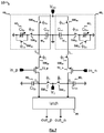
Fig.5 illustrates an embodiment of an input stage for a dynamic comparator according to the invention using external voltages Vhp and Vhn. -
Fig.6 illustrates an example of wide range of threshold voltages of a dynamic comparator achieved using the proposed input stage circuit. -
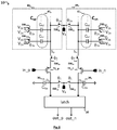
Fig.7 illustrates an implementation of a dynamic comparator comprising the proposed input stage using a charge-sharing DAC to internally generate the reset voltages Vhp and Vhn on the top plates of the capacitors Csp and Csn. -
Fig.8 illustrates an implementation of a dynamic comparator comprising the proposed input stage using a charge-redistribution DAC to internally generate the reset voltages Vhp and Vhn on the top plates of the capacitors Csp and Csn. -
Fig.9 illustrates an implementation of a dynamic comparator comprising the proposed input stage using a resistive DAC to internally generate the reset voltages Vhp and Vhn and provide them to the top plates of the capacitors Csp and Csn. -
Fig.10 illustrates an implementation of a dynamic comparator comprising the proposed input stage using a current DAC to internally generate the reset voltages Vhp and Vhn on the top plates of the capacitors Csp and Csn. -
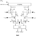
Fig.11 illustrates an implementation of a dynamic comparator comprising the proposed input stage using a programmable amplifier to internally generate the reset voltages Vhp and Vhn and provide them to the top plates of the capacitors Csp and Csn. -
Fig.12 illustrates an implementation containing a dynamic comparator according to the invention and mapping circuitry used to tune the threshold of the comparator. -
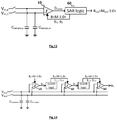
Fig.13 illustrates an implementation of a SAR ADC containing a dynamic comparator according to the invention where the threshold voltages are changed during the conversion. -
Fig.14 illustrates an ADC implementation containing multiple dynamic comparators according to the invention implementing an asynchronous search algorithm. - The present invention will be described with respect to particular embodiments and with reference to certain drawings but the invention is not limited thereto but only by the claims.
- Furthermore, the terms first, second and the like in the description and in the claims, are used for distinguishing between similar elements and not necessarily for describing a sequence, either temporally, spatially, in ranking or in any other manner. It is to be understood that the terms so used are interchangeable under appropriate circumstances and that the embodiments of the invention described herein are capable of operation in other sequences than described or illustrated herein.
- It is to be noticed that the term "comprising", used in the claims, should not be interpreted as being restricted to the means listed thereafter; it does not exclude other elements or steps. It is thus to be interpreted as specifying the presence of the stated features, integers, steps or components as referred to, but does not preclude the presence or addition of one or more other features, integers, steps or components, or groups thereof. Thus, the scope of the expression "a device comprising means A and B" should not be limited to devices consisting only of components A and B. It means that with respect to the present invention, the only relevant components of the device are A and B.
- Reference throughout this specification to "one embodiment" or "an embodiment" means that a particular feature, structure or characteristic described in connection with the embodiment is included in at least one embodiment of the present invention. Thus, appearances of the phrases "in one embodiment" or "in an embodiment" in various places throughout this specification are not necessarily all referring to the same embodiment, but may. Furthermore, the particular features, structures or characteristics may be combined in any suitable manner, as would be apparent to one of ordinary skill in the art from this disclosure, in one or more embodiments.
- Similarly it should be appreciated that in the description of exemplary embodiments of the invention, various features of the invention are sometimes grouped together in a single embodiment, figure, or description thereof for the purpose of streamlining the disclosure and aiding in the understanding of one or more of the various inventive aspects. This method of disclosure, however, is not to be interpreted as reflecting an intention that the claimed invention requires more features than are expressly recited in each claim. Rather, as the following claims reflect, inventive aspects lie in less than all features of a single foregoing disclosed embodiment. Thus, the claims following the detailed description are hereby expressly incorporated into this detailed description, with each claim standing on its own as a separate embodiment of this invention.
- Furthermore, while some embodiments described herein include some but not other features included in other embodiments, combinations of features of different embodiments are meant to be within the scope of the invention, and form different embodiments, as would be understood by those in the art. For example, in the following claims, any of the claimed embodiments can be used in any combination.
- It should be noted that the use of particular terminology when describing certain features or aspects of the invention should not be taken to imply that the terminology is being redefined herein to be restricted to include any specific characteristics of the features or aspects of the invention with which that terminology is associated.
- In the description provided herein, numerous specific details are set forth. However, it is understood that embodiments of the invention may be practiced without these specific details. In other instances, well-known methods, structures and techniques have not been shown in detail in order not to obscure an understanding of this description.
- The present invention proposes an input stage for a dynamic comparator with a simple architecture allowing the use of a single comparator for a wide range of threshold voltages. Further properties of the disclosed circuit comprise :
- small comparison time between sampling moment and a valid comparator result for high-speed applications
- low power consumption
- low input capacitance
- operation over a wide range of common-mode input values
- The proposed circuit is explained assuming a PMOS input pair, but it can also be applied to comparators with NMOS input pair. A scheme illustrating the general idea behind the proposed comparator is given in
Fig.5 . Compared to the conventional solution ofFig.2 , the source node of the differential input pair is split in two nodes Sip and Sin and two capacitors CSp and CSn are added to these nodes. The top plates are connected to the Sip and Sin nodes, while the bottom plates are connected to fixed voltages V2p and V2n, respectively. Note that the proposed circuit can also be realized with the top and bottom plates swapped. CSp and CSn represent the total capacitances on the nodes Sip and Sin, respectively, including all parasitic capacitance on these nodes. In the reset mode the top plate voltages of Csp and Csn are reset to independent voltages Vhp and Vhn depending on the comparator threshold voltage to realize as well as on the common-mode input level of the comparator. Also in the reset mode, the nodes Dip and Din are reset to a fixed voltage V1. During the comparison phase, the switches SW2p, SW2n are closed and the voltage on the nodes Dip and Din increases and builds up a difference until the threshold of the latch is achieved and a decision is made. -
Fig.5 shows an embodiment where the reset voltages Vhp and Vhn are provided via switches SW3p, SW3n. While the source nodes Sip and Sin are reset to a high voltage (Vhp,Vhn), the drain nodes Dip and Din (with some capacitance CD comprising the parasitic capacitance and, optionally, an extra capacitor, for example, to lower the noise) are reset to a fixed low voltage V1, usually the electrical ground and in general different from reset voltages Vhp and Vhn. Although the capacitors CDp and CDn are usually the same inFig.5 and the nodes Dip and Din are reset to the same voltage V1, different capacitors and/or voltages (e.g. V1p, V1n) might be used, for example to compensate for mismatch errors. During the comparison phase the switches SW2p and SW2n are closed and the voltages on the nodes Dip and Din increase at different rates depending on the input voltage and the high voltages Vhp, Vhn. Different implementations may choose to open or close the reset switches SW3p, SW3n during this comparison phase. Similar to the dynamic comparator used in the prior art, the latch circuit is triggered when the voltage difference on the nodes Dip and Din is large enough to generate the result of the comparison. In one implementation as inFig.5 extra switches SW7p and SW7n are added to the source nodes of the input transistors T1_p, T1_n to connect them to a fixed voltage (for example, the electrical ground) to put these nodes to a fixed voltage, when the switches SW2p and SW2n are open to realize a fixed input capacitance of the comparator while in reset phase. - The main difference with the conventional input pair of
Fig.2 is the source-gate voltage of the input pair when the input voltage is around the threshold voltage. If Vtn denotes the comparator threshold voltage and Vcm the common-mode input voltage, the input voltages on the positive (P) and negative (N) side are Vin_p = Vcm - Vth/2 and Vin_n = Vcm + Vtn/2. In a conventional input structure as inFig.2 , the source of both PMOS transistors is the same, resulting in one transistor having a large source-gate voltage while the other has a small source-gate voltage. In this input structure the N side would have a source-gate voltage of (VDD - Vsd) - (Vcm + Vth/2) with Vsd the required voltage over the top switch (or current source). To avoid turning off one side of the differential pair to obtain accurate comparison around the threshold voltage, this source-gate voltage should be larger than the absolute value of the threshold voltage VT of the transistor. With a common-mode voltage halfway the supply voltage, this poses an upper limit to the threshold voltage of VDD - 2Vsd - 2VT. For example, for a VDD = 800mV and aggressive values for Vds = 50mV and VT = 200 mV, this result in a maximum comparator threshold voltage of 300mV. - In the proposed architecture, however, the source voltage of each input transistor moves along with the target threshold voltage ensuring both transistors have the same overdrive voltage around the threshold point. As a result, a much wider range of threshold voltages can be realized.
-
Fig.6 shows simulation results of an implementation of the proposed technique in a 16nm technology with 800 mV supply voltage. The threshold voltage ranges from almost -600mV to +600mV. Due to the charge-sharing between the respective capacitors CSp, CSn and CDp, CDn the voltages at the source nodes drop during the comparison phase and as a result the threshold voltage of the comparator is somewhat larger than the voltage difference Vhp - Vhn to which CSp and CSn are reset. - Another disadvantage of the conventional implementation is that the input common-mode level is limited in the input pair to avoid turning off the transistors of the input pair which would make the comparator very slow. For example, a PMOS input pair with the same values for Vsd and VT as listed above operates for a maximum input common-value of VDD - Vsd - VT - Vth/2 which becomes 550mV when no threshold voltage Vth is programmed into the comparator. For higher input common-mode values, an NMOS input pair should be used. The input circuit according to this invention, however, overcomes this disadvantage as it allows continued use of a PMOS input pair for higher input values by putting the source of the input transistors also higher, which prevents turning them off.
- In the embodiment of
Fig.5 the voltages Vhp and Vhn are available as external voltages. Fixed capacitors Csp and Csn are used with a bottom plate connected to yet other external voltages V2p,V2n, for example the electrical ground. A practical implementation uses some buffer to provide the voltages Vhp and Vhn to one or more comparators. The time available to precharge the capacitors CSp and CSn is usually relaxed since it corresponds to the reset time of the comparator, which is at least equal to the tracking time of the sampler in a typical flash ADC or pipelined ADC. Consequently, the bandwidth of the external circuit (e.g. a buffer) used to provide the voltages Vhp and Vhn can be small, and small switches SW3p, SW3n can be used. As a result, only a small amount of power is required in the external circuits and to toggle the switches. - In other embodiments the voltages Vhp and Vhn are internally generated.
Fig.7 shows an example of a capacitor network that dynamically generates these voltages by charge-sharing between a fixed capacitor CSp, CSn with the bottom plate connected to the electrical ground and with the top plate connected to a tuneable capacitor CBp, CBn. This tuneable capacitor is usually built as an array of switchable capacitors. A digital code is used to select the number of capacitors and, hence, the size of CBp, CBn. The reset phase φ1 is split in two parts wherein during the first reset phase (φ1a) the capacitors CSp and CSn are reset to the supply voltage VDD via switches SW4p, SW4n and the capacitors CB are reset to the electrical ground via switches SW5p, SW5n. Then, during the second reset phase (φ1b), the top plates of CSp and CSn are connected to the capacitors CBp, CBn via switches SW6p, SW6n to generate the voltages Vhp, Vhn on the top plates of the capacitors CSp and CSn. As a result, the reset voltages Vhp and Vhn are now different from the initial reset voltages VDD and electrical ground. Instead of the supply voltage VDD, any fixed voltage can be used, be it lower or higher than VDD. For example, any conventional charge pump can be used to generate a voltage higher than VDD. - In another implementation the capacitors CBp and CBn are first precharged to fixed voltages and then connected either via the top or the bottom plate to the capacitors CSp, CSn, respectively, with the other plate to a fixed voltage (e.g. the electrical ground) to generate voltages Vhp and Vhn, similar to a charge-sharing DAC. In a fully differential implementation, only one tuneable capacitor CB is used which is also first precharged to a fixed voltage and then via the top and bottom plates connected to Sip, Sin or Sin, Sip to generate Vhp and Vhn.
- Another embodiment is shown in
Fig.8 . Here, the fixed capacitors Csp (41p) and CSn (41n) are both split into a plurality of capacitor units Cs1, Cs2... The bottom plates of these Csp and CSn can be switched between external voltages V2a, V2b. During the first reset phase (φ1a), the top plates of the respective capacitors CSp, CSn are reset to a fixed external voltage V3 (e.g., the supply voltage or the common-mode level) while the bottom plates of the units are connected to either V2a or V2b. In the second reset phase (φ1b) the bottom plates are switched to generate the reset voltages Vhp, Vhn at the top plates (similarly toFig.5 , but for simplicity not shown here). The voltages Vhp, Vhn are in general different from the fixed external voltage V3. In one implementation the bottom plates are switched to a higher voltage to generate the Vhp, Vhn voltages higher than VDD. Another implementation adds a fixed series capacitor between the common top plate of the capacitors and the source nodes Sip, Sin to realize effective low values of Csp and CSn without the need for physically small capacitors, which are very impractical. Smaller capacitors require less energy to be recharged, which may be desirable in low-power applications. Also, when Csp and Csn are made of units (as inFig.8 ), small capacitors may be desirable to realize a high tuning range resolution without getting a large sum, which would increase the power. - In yet another embodiment shown in
Fig.9 , the capacitors CSp, CSn are reset via switches SW3p, SW3n to nodes of which the voltages (Vhp, Vhn) are determined by the ratios of tuneable resistors 43, 44. These resistors can be made tuneable by putting resistor units in parallel or in series. In another implementation a fixed resistor ladder may be used, which generates different reference voltages. Via a network of switches the appropriate reference voltage can then be chosen to be connected to the respective nodes Sip, Sin. By adding tuneable resistors on top and/or bottom of the fixed resistor ladder, an attenuation factor can be applied to all reference voltages, for example, to match an attenuation of the input signal provided to the comparator. In yet another implementation an R-2R DAC comprising a network of parallel and series resistors, is used to generate the reference voltages which are connected to respective nodes Sip, Sin via a switch matrix. Since the reset time is usually relaxed, large resistors can be used to limit the static power consumption. In one implementation switches can be added in the resistive network to turn it completely off during the comparison phase and only activate the resistive network during the reset phase when the voltages Vhp and Vhn are to be generated. - The embodiment of
Fig.10 shows the voltages Vhp and Vhn being generated using current sources which are connected during a fixed time φ1b to the top plates of capacitors Csp and Csn. During φ1a these capacitors are first reset to a fixed voltage V0 (like the supply voltage, the electrical ground or the common-mode level, which in general is different from Vhp and Vhn). During the phase φ1b the current sources are putting a charge proportional to the current value and the time φ1b onto the capacitors CSp, CSn, which increases or decreases the voltages Vhp, Vhn accordingly. Hence, different values are readily generated by using programmable current sources, or by varying the reset time used to generate the voltages Vhp and Vhn. - Amplifiers or buffers can also be used to provide the voltages Vhp and Vhn. The embodiment of
Fig.11 shows two amplifiers with a tuneable gain Ap, An, which amplify a fixed reference signal Vref to the different voltages for the positive and negative branches. In one implementation a closed-loop amplifier containing an opamp, operational transconductance amplifier (OTA), switched opamp, ring amplifier or comparator with a resistive or capacitive feedback network, is used to generate different voltages by varying one or more resistors or capacitors. In another implementation an open-loop dynamic amplifier is used with tuneable amplification time to generate the different voltages. - In an embodiment the circuit according to the present invention (as implemented in any of the embodiments shown in
Fig.5 andFigs.7 to 11 ) is used for a coarse tuning of the threshold voltage while a fine tuning is realized conventionally, for example, with tuneable capacitors CDp and CDn, tuneable current sources at the nodes Dip and Din or tuneable bulk or substrate voltages for the input transistors. - In one implementation the input stage contains a mapping circuit, such as a combinatorial logic or a memory block like a look-up table which maps an input M-bit code B<M-1:0> onto two digital N-bit codes Bp<N-1:0> and Bn<N-1:0> which sets the threshold voltage according to any one of the embodiments mentioned above.
Fig.12 illustrates the use ofsuch mapping circuit 50 in the embodiment ofFig.5 . This configuration with a mapping circuit allows changing the threshold voltage or the common-mode input level during a data conversion algorithm. For example, as shown inFig.13 , aSAR logic 60 performing a SAR algorithm can be employed where the comparator threshold voltages are adapted in each step rather than the input voltage of the comparator. Another implementation, illustrated inFig.14 , uses multiple comparators with common input pins, which are subsequently activated, and whereby the threshold voltage of each comparator is set according to the results of the previous comparators. For example, the search logic inFig.14 implements an asynchronous binary search algorithm. - In yet another implementation the outputs of two input stages are combined, for example via resistors, to create interpolated output values which are used to trigger more than two latches. This architecture allows realizing comparisons with interpolated threshold voltages without the need for extra input stages which would increase the power and total input capacitance.
- The proposed solution ensures both input transistors see the same source-gate voltage around the threshold of the comparator without turning off one side when a large threshold voltage is required. Also, it allows operation with a wide range of input common-mode levels. For example, PMOS input transistors can be used for a high input level by putting both Vhp and Vhn at a higher level ensuring the gate-source voltage is large enough for correct operation.
- There is no need for a network in front of the comparator to subtract the threshold voltage from the input before comparing which otherwise increase the comparison time, the power and the total input capacitance and introduces non-linear attenuation of the input signal.
- The source capacitors CSp, CSn are precharged to Vhp, Vhn during the reset phase of the comparator, which is not in the critical timing path of typical flash and pipelined ADCs. As a result, there is no speed penalty.
- The basic efficiency regarding energy, input capacitance, timing and noise is the same as for the conventional dynamic comparator with the extra functionality of a high threshold available.
- To program the threshold voltage into the comparator, a simple calibration routine based can be employed. At the input of the comparator the threshold voltage at the desired common-mode input level is provided and the voltages Vhp, Vhn are varied until the comparator provides an equal numbers of ones and zeros.
- While the invention has been illustrated and described in detail in the drawings and foregoing description, such illustration and description are to be considered illustrative or exemplary and not restrictive. The foregoing description details certain embodiments of the invention. It will be appreciated, however, that no matter how detailed the foregoing appears in text, the invention may be practiced in many ways. The invention is not limited to the disclosed embodiments.
- Other variations to the disclosed embodiments can be understood and effected by those skilled in the art in practicing the claimed invention, from a study of the drawings, the disclosure and the appended claims. In the claims, the word "comprising" does not exclude other elements or steps, and the indefinite article "a" or "an" does not exclude a plurality. A single processor or other unit may fulfil the functions of several items recited in the claims. The mere fact that certain measures are recited in mutually different dependent claims does not indicate that a combination of these measures cannot be used to advantage. A computer program may be stored/distributed on a suitable medium, such as an optical storage medium or a solid-state medium supplied together with or as part of other hardware, but may also be distributed in other forms, such as via the Internet or other wired or wireless telecommunication systems. Any reference signs in the claims should not be construed as limiting the scope.
Claims (13)
- Input circuit for a dynamic comparator comprising a positive and a negative branch, each branch comprising a transistor (T1_n, T1_p) arranged for receiving an input voltage (Vin,p, Vin,n) at its gate terminal and a first fixed voltage (V1) at its drain terminal (Dip, Din) via a first switch (SW1n, SW1p) characterised in that the source terminal of said transistor in each of said positive and negative branch is connectable via a second switch (SW2n, SW2p) to a first plate (Sip, Sin) of a first capacitor (CSp) in said positive branch and of a second capacitor (CSn) in said negative branch, respectively, with a second plate of said first capacitor and of said second capacitor being connected to a second fixed voltage (V2p, V2n) and said input circuit further being arranged for receiving a first reset voltage (Vhp) on said first plate of said first capacitor in said positive branch and a second reset voltage (Vhn) on said first plate of said second capacitor in said negative branch, said first and said second reset voltage being independent of each other.
- Input circuit for a dynamic comparator as in claim 1, wherein said first (Vhp) and said second (Vhn) reset voltage are provided by an external voltage.
- Input circuit for a dynamic comparator as in claim 1, wherein said first and said second reset voltage are provided via a resistive network.
- Input circuit for a dynamic comparator as in claim 1, wherein said first and said second reset voltage are provided via a capacitive network.
- Input circuit for a dynamic comparator as in claim 1, wherein said first capacitor and said second capacitor are implemented as a switchable capacitive network arranged to be precharged to a fixed voltage and switched to generate said first and second reset voltage.
- Input circuit as in claim 1, wherein said first and said second reset voltage are provided via amplifiers with fixed or tuneable gain values.
- Input circuit for a dynamic comparator as in claim 1, comprising transistors arranged for acting as current sources (Ip, In) to generate said first and said second reset voltage.
- Input circuit as in any of the previous claims, comprising a latch circuit arranged for receiving a first signal output from said positive branch and a second signal output from said negative branch.
- Input circuit as in claim 8, wherein said latch circuit is arranged for being triggered when a voltage difference between said output nodes reaches a given threshold level.
- Input circuit as in claim 1, wherein said transistors in said branches are PMOS transistors.
- Input circuit as in claim 1, wherein said transistors in said branches are NMOS transistors.
- Comparator (10) comprising an input circuit as in any of the previous claims.
- Analog-to-digital converter comprising a comparator as in claim 11.
Priority Applications (2)
| Application Number | Priority Date | Filing Date | Title |
|---|---|---|---|
| EP16201696.8A EP3331162A1 (en) | 2016-12-01 | 2016-12-01 | Input circuit for a dynamic comparator |
| US15/826,668 US10090852B2 (en) | 2016-12-01 | 2017-11-29 | Input circuit for a dynamic comparator |
Applications Claiming Priority (1)
| Application Number | Priority Date | Filing Date | Title |
|---|---|---|---|
| EP16201696.8A EP3331162A1 (en) | 2016-12-01 | 2016-12-01 | Input circuit for a dynamic comparator |
Publications (1)
| Publication Number | Publication Date |
|---|---|
| EP3331162A1 true EP3331162A1 (en) | 2018-06-06 |
Family
ID=57482220
Family Applications (1)
| Application Number | Title | Priority Date | Filing Date |
|---|---|---|---|
| EP16201696.8A Ceased EP3331162A1 (en) | 2016-12-01 | 2016-12-01 | Input circuit for a dynamic comparator |
Country Status (2)
| Country | Link |
|---|---|
| US (1) | US10090852B2 (en) |
| EP (1) | EP3331162A1 (en) |
Cited By (3)
| Publication number | Priority date | Publication date | Assignee | Title |
|---|---|---|---|---|
| CN108768352A (en) * | 2018-07-17 | 2018-11-06 | 上海艾为电子技术股份有限公司 | Comparator |
| CN117278004A (en) * | 2023-11-21 | 2023-12-22 | 拓尔微电子股份有限公司 | Comparison circuit |
| CN118017985A (en) * | 2024-04-10 | 2024-05-10 | 深圳市赛元微电子股份有限公司 | Dynamic latching comparator |
Families Citing this family (7)
| Publication number | Priority date | Publication date | Assignee | Title |
|---|---|---|---|---|
| CN110474623B (en) * | 2019-07-08 | 2021-01-12 | 浙江大学 | An offset self-correcting dynamic comparator for successive approximation analog-to-digital converters |
| CN111313872B (en) * | 2020-02-23 | 2023-05-09 | 电子科技大学 | A Dynamic Latch Comparator with High Resolution and Low Power Consumption |
| CN112953420B (en) * | 2021-03-22 | 2022-09-09 | 电子科技大学 | A dynamic operational amplifier circuit with input tube in linear region |
| TWI791248B (en) * | 2021-07-26 | 2023-02-01 | 新唐科技股份有限公司 | Dynamic comparator and circuit system using the same |
| US11736016B2 (en) | 2021-08-25 | 2023-08-22 | Dialog Semiconductor (Uk) Limited | Switching converter with improved load transient response and method of operating the same |
| CN116488622B (en) * | 2023-04-03 | 2024-02-02 | 广东工业大学 | Low-power consumption dynamic comparator |
| CN117176083B (en) * | 2023-08-11 | 2024-09-10 | 深圳高铂科技有限公司 | Pre-amplifying circuit for detecting voltage level of high-speed large-swing signal |
Citations (2)
| Publication number | Priority date | Publication date | Assignee | Title |
|---|---|---|---|---|
| JP2012039548A (en) * | 2010-08-11 | 2012-02-23 | Renesas Electronics Corp | Dynamic amplifier |
| US9236855B2 (en) * | 2011-11-03 | 2016-01-12 | Mediatek Inc. | Comparator and amplifier |
Family Cites Families (5)
| Publication number | Priority date | Publication date | Assignee | Title |
|---|---|---|---|---|
| US6542019B1 (en) * | 2001-11-28 | 2003-04-01 | Berkäna Wireless, Inc. | Highly linear and low noise figure mixer |
| EP2557687B1 (en) * | 2011-08-11 | 2018-06-13 | Telefonaktiebolaget LM Ericsson (publ) | Low-noise amplifier, receiver, method and computer program |
| US9124279B2 (en) * | 2012-09-03 | 2015-09-01 | Tensorcom, Inc. | Method and apparatus for an active negative-capacitor circuit to cancel the input capacitance of comparators |
| US9853615B2 (en) * | 2016-04-13 | 2017-12-26 | Avago Technologies General Ip (Singapore) Pte. Ltd. | Linearized dynamic amplifier |
| US10483911B2 (en) * | 2016-09-16 | 2019-11-19 | Intel Corporation | MOS transistor-based RF switch topologies for high speed capacitive tuning of oscillators |
-
2016
- 2016-12-01 EP EP16201696.8A patent/EP3331162A1/en not_active Ceased
-
2017
- 2017-11-29 US US15/826,668 patent/US10090852B2/en active Active
Patent Citations (2)
| Publication number | Priority date | Publication date | Assignee | Title |
|---|---|---|---|---|
| JP2012039548A (en) * | 2010-08-11 | 2012-02-23 | Renesas Electronics Corp | Dynamic amplifier |
| US9236855B2 (en) * | 2011-11-03 | 2016-01-12 | Mediatek Inc. | Comparator and amplifier |
Non-Patent Citations (4)
| Title |
|---|
| MASAYA MIYAHARA ET AL: "A low-offset latched comparator using zero-static power dynamic offset cancellation technique", SOLID-STATE CIRCUITS CONFERENCE, 2009. A-SSCC 2009. IEEE ASIAN, IEEE, PISCATAWAY, NJ, USA, 16 November 2009 (2009-11-16), pages 233 - 236, XP031582956, ISBN: 978-1-4244-4433-5 * |
| NUZZO P ET AL: "Noise Analysis of Regenerative Comparators for Reconfigurable ADC Architectures", IEEE TRANSACTIONS ON CIRCUITS AND SYSTEMS I: REGULAR PAPERS, IEEE, US, vol. 55, no. 6, 1 July 2008 (2008-07-01), pages 1441 - 1454, XP011333157, ISSN: 1549-8328, DOI: 10.1109/TCSI.2008.917991 * |
| RABUSKE TAIMUR ET AL: "Comparator-based binary-search ADC architectures for UWB receivers", ANALOG INTEGRATED CIRCUITS AND SIGNAL PROCESSING, SPRINGER NEW YORK LLC, US, vol. 77, no. 3, 8 October 2013 (2013-10-08), pages 471 - 482, XP035311542, ISSN: 0925-1030, [retrieved on 20131008], DOI: 10.1007/S10470-013-0195-7 * |
| YONG CHEN ET AL: "Comparator with built-in reference voltage generation and split-ROM encoder for a high-speed flash ADC", 2015 INTERNATIONAL SYMPOSIUM ON SIGNALS, CIRCUITS AND SYSTEMS (ISSCS), 10 July 2015 (2015-07-10), Iasi, Romania, pages 1 - 4, XP055374330, ISBN: 978-1-4673-7488-0, DOI: 10.1109/ISSCS.2015.7203923 * |
Cited By (4)
| Publication number | Priority date | Publication date | Assignee | Title |
|---|---|---|---|---|
| CN108768352A (en) * | 2018-07-17 | 2018-11-06 | 上海艾为电子技术股份有限公司 | Comparator |
| CN108768352B (en) * | 2018-07-17 | 2023-11-03 | 上海艾为电子技术股份有限公司 | Comparator with a comparator circuit |
| CN117278004A (en) * | 2023-11-21 | 2023-12-22 | 拓尔微电子股份有限公司 | Comparison circuit |
| CN118017985A (en) * | 2024-04-10 | 2024-05-10 | 深圳市赛元微电子股份有限公司 | Dynamic latching comparator |
Also Published As
| Publication number | Publication date |
|---|---|
| US10090852B2 (en) | 2018-10-02 |
| US20180159549A1 (en) | 2018-06-07 |
Similar Documents
| Publication | Publication Date | Title |
|---|---|---|
| US10090852B2 (en) | Input circuit for a dynamic comparator | |
| US10103742B1 (en) | Multi-stage hybrid analog-to-digital converter | |
| US7741981B1 (en) | Dual-use comparator/op amp for use as both a successive-approximation ADC and DAC | |
| US8416107B1 (en) | Charge compensation calibration for high resolution data converter | |
| US7511648B2 (en) | Integrating/SAR ADC and method with low integrator swing and low complexity | |
| US7764215B2 (en) | Multi-stage comparator with offset canceling capacitor across secondary differential inputs for high-speed low-gain compare and high-gain auto-zeroing | |
| US8754794B1 (en) | Methods and apparatus for calibrating pipeline analog-to-digital converters | |
| US9698813B2 (en) | Input buffer and analog-to-digital converter | |
| US6169502B1 (en) | Pipelined analog-to-digital converter (ADC) systems, methods, and computer program products | |
| US20150015307A1 (en) | Comparator and amplifier | |
| JP6114390B2 (en) | Analog to digital converter | |
| CN111565042B (en) | Correction method suitable for two-step ADC | |
| CN107863962B (en) | Capacitance Adaptation Error Calibration System for High Precision Charge Domain Pipeline ADC | |
| GB2393055A (en) | A transconductance amplifier with input sampling capacitor for a current-interpolating A-D converter | |
| US11855651B2 (en) | Discrete-time offset correction circuit embedded in a residue amplifier in a pipelined analog-to-digital converter (ADC) | |
| US7030799B2 (en) | Current-steering digital-to-analog converter | |
| CN113098511A (en) | Front-end self-calibration method of pipeline successive approximation type analog-to-digital converter | |
| US6850181B1 (en) | Apparatus and method for noise reduction for a successive approximation analog-to-digital converter circuit | |
| US10476513B1 (en) | SAR ADC with high linearity | |
| CA2494264C (en) | Switched capacitor system, method, and use | |
| CN109286398B (en) | Current comparator and comparison method for correcting current steering digital-to-analog converter | |
| US10574255B2 (en) | Multiplying digital-to-analog conversion circuit | |
| TWI777464B (en) | Signal converting apparatus and signal converting method | |
| US7372389B2 (en) | Analogue to digital converter, and method of analogue to digital conversion | |
| CN223274106U (en) | Display devices, chips, analog-to-digital converters |
Legal Events
| Date | Code | Title | Description |
|---|---|---|---|
| PUAI | Public reference made under article 153(3) epc to a published international application that has entered the european phase |
Free format text: ORIGINAL CODE: 0009012 |
|
| STAA | Information on the status of an ep patent application or granted ep patent |
Free format text: STATUS: THE APPLICATION HAS BEEN PUBLISHED |
|
| AK | Designated contracting states |
Kind code of ref document: A1 Designated state(s): AL AT BE BG CH CY CZ DE DK EE ES FI FR GB GR HR HU IE IS IT LI LT LU LV MC MK MT NL NO PL PT RO RS SE SI SK SM TR |
|
| AX | Request for extension of the european patent |
Extension state: BA ME |
|
| STAA | Information on the status of an ep patent application or granted ep patent |
Free format text: STATUS: REQUEST FOR EXAMINATION WAS MADE |
|
| 17P | Request for examination filed |
Effective date: 20181206 |
|
| RBV | Designated contracting states (corrected) |
Designated state(s): AL AT BE BG CH CY CZ DE DK EE ES FI FR GB GR HR HU IE IS IT LI LT LU LV MC MK MT NL NO PL PT RO RS SE SI SK SM TR |
|
| STAA | Information on the status of an ep patent application or granted ep patent |
Free format text: STATUS: EXAMINATION IS IN PROGRESS |
|
| 17Q | First examination report despatched |
Effective date: 20200729 |
|
| APBK | Appeal reference recorded |
Free format text: ORIGINAL CODE: EPIDOSNREFNE |
|
| APBN | Date of receipt of notice of appeal recorded |
Free format text: ORIGINAL CODE: EPIDOSNNOA2E |
|
| APBR | Date of receipt of statement of grounds of appeal recorded |
Free format text: ORIGINAL CODE: EPIDOSNNOA3E |
|
| APAF | Appeal reference modified |
Free format text: ORIGINAL CODE: EPIDOSCREFNE |
|
| APAF | Appeal reference modified |
Free format text: ORIGINAL CODE: EPIDOSCREFNE |
|
| APBT | Appeal procedure closed |
Free format text: ORIGINAL CODE: EPIDOSNNOA9E |
|
| STAA | Information on the status of an ep patent application or granted ep patent |
Free format text: STATUS: THE APPLICATION HAS BEEN REFUSED |
|
| 18R | Application refused |
Effective date: 20241111 |