US11736016B2 - Switching converter with improved load transient response and method of operating the same - Google Patents
Switching converter with improved load transient response and method of operating the same Download PDFInfo
- Publication number
- US11736016B2 US11736016B2 US17/411,319 US202117411319A US11736016B2 US 11736016 B2 US11736016 B2 US 11736016B2 US 202117411319 A US202117411319 A US 202117411319A US 11736016 B2 US11736016 B2 US 11736016B2
- Authority
- US
- United States
- Prior art keywords
- panic
- comparator
- switching converter
- latch
- output
- Prior art date
- Legal status (The legal status is an assumption and is not a legal conclusion. Google has not performed a legal analysis and makes no representation as to the accuracy of the status listed.)
- Active
Links
Images


Classifications
-
- H—ELECTRICITY
- H02—GENERATION; CONVERSION OR DISTRIBUTION OF ELECTRIC POWER
- H02M—APPARATUS FOR CONVERSION BETWEEN AC AND AC, BETWEEN AC AND DC, OR BETWEEN DC AND DC, AND FOR USE WITH MAINS OR SIMILAR POWER SUPPLY SYSTEMS; CONVERSION OF DC OR AC INPUT POWER INTO SURGE OUTPUT POWER; CONTROL OR REGULATION THEREOF
- H02M3/00—Conversion of dc power input into dc power output
- H02M3/02—Conversion of dc power input into dc power output without intermediate conversion into ac
- H02M3/04—Conversion of dc power input into dc power output without intermediate conversion into ac by static converters
- H02M3/10—Conversion of dc power input into dc power output without intermediate conversion into ac by static converters using discharge tubes with control electrode or semiconductor devices with control electrode
- H02M3/145—Conversion of dc power input into dc power output without intermediate conversion into ac by static converters using discharge tubes with control electrode or semiconductor devices with control electrode using devices of a triode or transistor type requiring continuous application of a control signal
- H02M3/155—Conversion of dc power input into dc power output without intermediate conversion into ac by static converters using discharge tubes with control electrode or semiconductor devices with control electrode using devices of a triode or transistor type requiring continuous application of a control signal using semiconductor devices only
- H02M3/156—Conversion of dc power input into dc power output without intermediate conversion into ac by static converters using discharge tubes with control electrode or semiconductor devices with control electrode using devices of a triode or transistor type requiring continuous application of a control signal using semiconductor devices only with automatic control of output voltage or current, e.g. switching regulators
- H02M3/158—Conversion of dc power input into dc power output without intermediate conversion into ac by static converters using discharge tubes with control electrode or semiconductor devices with control electrode using devices of a triode or transistor type requiring continuous application of a control signal using semiconductor devices only with automatic control of output voltage or current, e.g. switching regulators including plural semiconductor devices as final control devices for a single load
- H02M3/1584—Conversion of dc power input into dc power output without intermediate conversion into ac by static converters using discharge tubes with control electrode or semiconductor devices with control electrode using devices of a triode or transistor type requiring continuous application of a control signal using semiconductor devices only with automatic control of output voltage or current, e.g. switching regulators including plural semiconductor devices as final control devices for a single load with a plurality of power processing stages connected in parallel
- H02M3/1586—Conversion of dc power input into dc power output without intermediate conversion into ac by static converters using discharge tubes with control electrode or semiconductor devices with control electrode using devices of a triode or transistor type requiring continuous application of a control signal using semiconductor devices only with automatic control of output voltage or current, e.g. switching regulators including plural semiconductor devices as final control devices for a single load with a plurality of power processing stages connected in parallel switched with a phase shift, i.e. interleaved
-
- H—ELECTRICITY
- H02—GENERATION; CONVERSION OR DISTRIBUTION OF ELECTRIC POWER
- H02M—APPARATUS FOR CONVERSION BETWEEN AC AND AC, BETWEEN AC AND DC, OR BETWEEN DC AND DC, AND FOR USE WITH MAINS OR SIMILAR POWER SUPPLY SYSTEMS; CONVERSION OF DC OR AC INPUT POWER INTO SURGE OUTPUT POWER; CONTROL OR REGULATION THEREOF
- H02M1/00—Details of apparatus for conversion
- H02M1/32—Means for protecting converters other than automatic disconnection
-
- H—ELECTRICITY
- H02—GENERATION; CONVERSION OR DISTRIBUTION OF ELECTRIC POWER
- H02M—APPARATUS FOR CONVERSION BETWEEN AC AND AC, BETWEEN AC AND DC, OR BETWEEN DC AND DC, AND FOR USE WITH MAINS OR SIMILAR POWER SUPPLY SYSTEMS; CONVERSION OF DC OR AC INPUT POWER INTO SURGE OUTPUT POWER; CONTROL OR REGULATION THEREOF
- H02M1/00—Details of apparatus for conversion
- H02M1/0003—Details of control, feedback or regulation circuits
- H02M1/0009—Devices or circuits for detecting current in a converter
Definitions
- the present disclosure relates generally to a switching converter with improved load transient response, which may include a multi-phase implementation. More particularly, the disclosure relates to a panic comparator and method of operating.
- One of the challenges for buck converters is to achieve a good load transient response.
- the device should compensate the lack of the output current as quickly as possible to avoid large undershoot of the output voltage.
- One of the solutions is having a so-called “panic” comparator in the device. If the comparator detects the excess output voltage drop, the device instantly forces the high side switching device “on”.
- FIG. 1 shows 100 , one implementation of a switching converter having a panic comparator, known to the inventors.
- Output stage 110 , PWM generator 120 , and Error amp 130 comprise Main loop 140 . It regulates Vout to the target voltage while the load current is stable.
- Panic comparator 150 is also shown, as part of subsidiary loop 160 . It trips when the output voltage goes down below a predetermined threshold, which is lower than the target voltage.
- the output of the panic comparator is OR-ed with the PWM generator output and used as the on signal of the high side switching device and prevents large undershoot.
- the output voltage of the switching converter is regulated to the target voltage defined by the reference Vref in FIG. 1 .
- the threshold of the panic comparator is set slightly lower than the target voltage to avoid frequent reaction. There are two ways to generate the threshold. One way is to implement an offset to the differential input of the panic comparator. The voltage source 170 in FIG. 1 represents the implemented offset. Another way to generate the threshold is to generate the offset reference voltage using an amplifier, but this is not preferable because it requires additional blocks.
- FIG. 2 shows 200 , a timing chart of the switching converter of FIG. 1 .
- the panic comparator 250 forces the high side switching device to turn on.
- the output current 230 continues to increase as far as the panic comparator is asserted.
- the output current is more than the load current because of delay in the panic comparator. As a result, the output current exceeds the load current. It causes large overshoot of the output voltage because it takes a certain time to reduce the output current and Vout continues to increase while the output current is larger than the load.
- the panic comparator is modelled as a transconductance (gm) and buffer. There is a parasitic capacitance at the gm output.
- the transconductance translates voltage error between Vout and the panic comparator threshold vth_pnc into current.
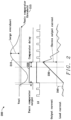
- FIG. 3 shows 300 , an additional timing chart of the FIG. 1 switching converter.
- output voltage Vout 310 goes below panic comparator threshold vth_pnc 315
- the transconductance (gm) starts to charge capacitance of gmout 355 .
- gmout voltage reaches buffer threshold vth_buf 360
- panic comparator output 350 is asserted.
- the gmout voltage continues to go up and run away from the buffer threshold.
- Vout goes up again and reaches vth_pnc
- transconductance gm starts to discharge gmout. It takes some time to reset the panic comparator output, because the gmout voltage is far away from vth_buf and the change of gmout is low due to small voltage error.
- the gmout could be clamped, but the clamp's effect would be limited because the clamp voltage could not be close to the buffer threshold.
- a switching converter with improved load transient response comprising a panic comparator, comprising a reset switch, a panic latch that is set by an output of the panic comparator and reset when the output is low at a strobe timing, and a timing generator which generates reset and strobe signals.
- the above and other objects of the present disclosure may be further accomplished with a method of operating a switching converter with improved load transient response.
- the steps include providing a panic comparator, comprising a reset switch.
- the steps also include setting a panic latch with an output of the panic comparator and resetting the panic latch in conjunction with a strobe timing.
- the steps also include generating reset and strobe signals with a timing generator.
- the timing generator is comprised of a gated oscillator (OSC), enabled by the panic latch.
- OSC gated oscillator
- the panic comparator comprises a High Pass Filter (HPF) element, configured to accelerate the panic comparator response.
- HPF High Pass Filter
- the switching converter is multi-phase.
- FIG. 1 shows one implementation of a switching converter having a panic comparator, known to the inventors.
- FIG. 2 shows a timing chart of the switching converter of FIG. 1 , when an output voltage goes below a panic comparator threshold.
- FIG. 3 shows an additional timing chart of the FIG. 1 switching converter, when a transconductance starts to charge the parasitic capacitance.
- FIG. 4 shows a block diagram of the present disclosure, for a panic comparator and its control, for a single-phase switching converter.
- FIG. 5 A shows a timing chart of the FIG. 4 switching converter.
- FIGS. 5 B and 5 C show state diagrams of the gated oscillator (OSC) and panic control of FIG. 4 .
- FIG. 6 A shows a block diagram of the present disclosure, for a panic comparator and its control, for a multi-phase buck switching converter.
- FIG. 6 B shows a circuit diagram of the High Pass Filter (HPF) element, for a panic comparator of FIG. 6 A .
- HPF High Pass Filter
- FIG. 6 C shows the monitoring of only dVout/dt, when the panic latch is asserted.
- FIGS. 7 A and 7 B show simulation results comparing output voltage, inductor current, and the panic comparator output, with and without the FIG. 6 switching converter, configured for four phases.
- FIG. 8 is a flow chart of a method for operation of the disclosed switching converter.
- FIG. 9 is a flow chart providing details of a method for operation of the disclosed switching converter.
- the present disclosure proposes a switching converter with improved load transient response.
- a panic comparator and method of operating the same is achieved by setting the panic comparator output low early, and without delay, to avoid a large overshoot after a panic reaction. Not only is the delay of the panic comparator reduced, but the panic comparator output is also set low when the output voltage approaches a threshold.
- Important features of the disclosure include a switching regulator with a panic comparator and its control, a reset switch connected to the critical or slowest node of the panic comparator, a panic latch which is set by the panic comparator output and reset when the panic comparator output is low at a strobe timing, and a timing generator which generates two signals as far as the latch is asserted.
- the two signals include a reset signal for the panic comparator and a strobe signal for the latch.
- Optional features include a timing generator comprised of a gated oscillator, enabled by the panic latch.
- Additional optional features include a panic comparator comprised of an HPF element, to accelerate its response.
- the HPF element monitors [(Vout ⁇ Vthg)+ ⁇ *dVout/dt] rather than a simple voltage error: (Vout ⁇ Vtgt).
- the HPF element can monitor [(Vout ⁇ Vtgt)+ ⁇ *dVout/dt] while the panic latch is low, and only monitors dVout/dt while the panic latch is high.
- the buck switching converter can be multi-phase.
- FIG. 4 shows 400 , a block diagram of the present disclosure, for a panic comparator and its control, for a single-phase switching converter. Differences from the prior art of FIG. 1 include Reset switch 416 added to panic comparator 450 and its control 410 .
- the Reset switch is connected to gmout of the panic comparator and forces gmout to a reset level.
- Control of a panic state is composed of panic latch 412 and gated oscillator (OSC) 415 as a timing generator.
- the signal latched cmpout is used for forcing the high side switching device “on” instead of signal cmpout from the panic comparator.
- Gated OSC is activated when latched cmpout is asserted and generates strobe 414 and cmp_rst 413 signals periodically.
- Panic latch 412 has set and reset input signals as shown, based on cmpout and strobe signals. Further details are provided in FIG. 5 A .
- FIG. 5 A shows 500 , a timing chart of the FIG. 4 switching converter.
- panic comparator output cmpout 550 is asserted and panic latch 412 is set, as shown by signal latched cmpout 520 .
- the gated oscillator is enabled as the timing generator, on strobe 540 .
- the timing generator generates very short pulses for panic comparator reset cmp_rst 530 immediately, and the voltage at gmout 555 is reset at each assertion of cmp_rst.
- Cmpout is reset accordingly.
- Cmp_rst is generated periodically, and when it is reset, gmout is charged up or down depending on the voltage error detected.
- the gated oscillator generates the strobe signal 540 periodically. If cmpout 550 is low at the strobe timing, the panic latch 520 is reset. If cmpout is high at the strobe timing, the panic latch is kept high. Polarity of cmpout at the strobe timing depends on the voltage error from vth_pnc 515 . If Vout 510 is far below vth_pnc, gmout 555 is charged up quickly after reset, and cmpout is high at the strobe timing. If the voltage error is small, gmout cannot reach buffer threshold vth_buf 560 and cmpout is low. Thus, the panic latch is reset when Vout approaches panic threshold, vth_pnc.
- Strobe signal 540 preferably starts a cycle after panic comparator reset cmp_rst 530 .
- the strobe is kept for a cycle after cmp_rst, because the panic comparator output does not reflect the actual voltage error during that period. Even if Vout is lower than the panic comparator threshold, vth_pnc 515 , it takes some time for gmout 555 to reach Vth_buf 560 .
- Latched cmpout 520 goes down, then back up, then back down again, towards the end of FIG. 5 A because while latched cmpout 520 is high, it can be reset only when strobe signal is high and cmpout is low.
- Latched cmpout 520 is kept high because cmpout 550 is high for the 1 st to 7 th pulses of strobe signal 540 .
- latched cmpout 520 is reset because cmpout 550 is low at that timing.
- latched cmpout 520 is low, gmout gradually rises as Vout is slightly lower than Vth_pnc.
- cmpout 550 When gmout reaches Vth_buf, cmpout 550 is asserted and it sets latched cmpout 520 again. After a cycle, the 9 th pulse of strobe signal 540 is generated. Latched cmpout 520 is reset at that timing because Vout is above Vth_pnc and cmpout 550 is not high.
- FIGS. 5 B and 5 C show state diagrams of the gated oscillator (OSC) and panic control of FIG. 4 .
- FIGS. 5 B and 5 C show the relationship between latched_cmpout as an input, and cmp_rst and strobe as outputs of the gated OSC. While latched cmpout is low, the gated OSC is disabled. When latched cmpout is asserted, the sequence is started and maintained while the latched cmpout is high. First, the cmp_rst pulse is generated, and there is a delay of a time period, dozens of nanoseconds, for example. Then the gated OSC generates the strobe pulse and returns the cmp_rst pulse again. Together with the panic latch 412 , the gated OSC functions as the panic control 410 in FIG. 4 .
- pncout 250 is asserted longer than ideal due to the delay of a panic comparator of the prior art. This is avoided in the disclosed switching converter of FIG. 4 , where the unwanted delay on the falling edge has been removed. This is best understood by modelling the panic comparator with a transconductance (gm) and buffer. Gm translates the voltage error between the Vout and Vth_pnc outputs into a current, and the gm output current is stored in the parasitic capacitance of gmout. When gmout voltage hits threshold Vth_buf voltage, the panic comparator of the present disclosure changes its output polarity.
- pncout 350 should ideally be reset when Vout reaches vthn_pnc. Since excessive charge is stored in the parasitic capacitance of gmout while Vout is lower than vth_pnc, the gmout voltage is far from vth_buf at that timing. As a result, it takes longer to discharge the gmput voltage to vth_buf, causing the delay.
- resetting of the panic latch is judged at the strobe timing. Since the parasitic capacitance of gmout is reset at the beginning of every cycle, the panic latch reset is not affected as much by excessive charge. Delay due to the gated OSC cycle can be ignored by setting the cycle short enough.
- FIG. 6 A shows 600 , a block diagram of the present disclosure, for a panic comparator and its control, for a multi-phase buck switching converter.
- current balance amp 640 is added.
- the current balance amp compares the sensed output currents of the phases, current sense 1 642 and current sense 2 644 , and adjusts the error amplifier output for the second phase.
- One way to measure the sensed output currents is to check the voltage drop across the switching devices of the output stages. In this case, the currents are sensed from the voltage drop across the low side devices while they are turned on.
- the panic comparator and its control are implemented as in FIG. 4 .
- the panic latch When the panic latch is asserted, the high side devices of both phases are turned on, and the output currents are increased.
- optional HPF element 670 is added to panic comparator 650 , adding a differential component to voltage of gmout.
- the HPF element improves the response further, because the panic comparator can anticipate Vout as a first order Taylor expansion given below: V out( t + ⁇ ) ⁇ V out+ ⁇ * dV out/ dt
- FIG. 6 B shows a circuit diagram of the High Pass Filter (HPF) element, for the panic comparator of FIG. 6 A .
- HPF High Pass Filter
- Another option is to only monitor dVout/dt when the panic latch is asserted, as shown in FIG. 6 C .
- Gm is disconnected with switch 675 , when latched cmpout is asserted. If the panic latch is asserted for too long of time, the inductor current would exceed the load current by too much. Since dVout/dt is proportional to the excess output current, this condition can be prevented by only monitoring dVout/dt.
- FIGS. 7 A and 7 B show simulation results comparing output voltage, inductor current, and the panic comparator output, with and without the circuitry of the FIG. 6 switching converter.
- the simulation results were based on a four-phase buck switching converter.
- the 710 and 720 waveforms show the output voltages of the switching converters.
- the 710 signal is the waveform of the prior art, using the circuit of FIG. 1 , in a four-phase configuration.
- the 720 signal is the waveform of the disclosure, using the circuit of FIG. 6 , in a four-phase configuration.
- Dotted line 725 represents the reference voltage, to which the output voltages are regulated.
- the output voltage 720 with the present disclosure panic comparator and its controls, has less overshoot than the output voltage 710 of the prior art.
- the 730 and 740 waveforms show the output/inductor currents of the switching converters.
- the 730 signal is the waveform of prior art
- 740 signal is the waveform of the disclosure.
- the 750 and 760 waveforms show the panic comparator outputs of the switching converters.
- the 750 signal is the waveform of the prior art and represents the direct output of the panic comparator.
- the 760 signal is the waveform of the disclosure and represents the latched panic comparator output. When the output voltage drops, the 760 signal is asserted. As long as the 760 signal remains high, the high side devices of the four phases of the buck switching converter are forced on, and their output currents continue to increase. In the prior art, the panic comparator output stays high after the output currents reach the load current, and even after the output voltage exceeds the reference voltage. This results in excess output current and causes a large overshoot of the output voltage.
- the panic comparator output is stopped faster, and overshoot is prevented.
- the output voltage error is small, latched cmpout becomes a short pulse from a continuous long pulse. It is a softer response than the prior art, and preferable for avoiding overshoot of the output voltage.
- FIG. 8 is flow chart 800 , of a method for operation of the disclosed switching converter.
- the steps include 810 , providing a panic comparator, comprising a reset switch.
- the steps also include 820 , setting a panic latch with an output of the panic comparator and resetting the panic latch in conjunction with a strobe timing.
- the steps also include 830 , generating reset and strobe signals with a timing generator.
- FIG. 9 is flow chart 900 , providing details of a method for operation of the disclosed switching converter.
- the steps include 910 , waiting for a large undershoot in the switching converter by checking the panic comparator, and 920 when the panic comparator is high, forcing a high side device on, and resetting the panic comparator.
- the steps also include 930 , releasing the panic comparator and waiting a time and 940 , checking the panic comparator again. If the panic comparator is high, forcing a high side device on, and resetting the panic comparator. If the panic comparator is low, return to waiting for a large undershoot in the switching converter by checking the panic comparator.
- the main advantage of one or more embodiments of the present disclosure include a switching converter with an improved load transient response, especially in a multi-phase implementation.
- the panic comparator is most effective for a buck switching converter with a small inductor on its output. With multi-phases and multiple inductors, all the phases are turned on if the panic pulse is asserted. Since the overall effective inductance is small, rapid control of the panic pulse may be achieved.
Abstract
Description
Vout(t+τ)˜Vout+τ*dVout/dt
Iout_hpf=−gm*Rf*Cin*d/dt(Vin_hpf)
Claims (29)
Priority Applications (2)
| Application Number | Priority Date | Filing Date | Title |
|---|---|---|---|
| US17/411,319 US11736016B2 (en) | 2021-08-25 | 2021-08-25 | Switching converter with improved load transient response and method of operating the same |
| DE102021127694.2A DE102021127694A1 (en) | 2021-08-25 | 2021-10-25 | Switching converter and method of operating the same |
Applications Claiming Priority (1)
| Application Number | Priority Date | Filing Date | Title |
|---|---|---|---|
| US17/411,319 US11736016B2 (en) | 2021-08-25 | 2021-08-25 | Switching converter with improved load transient response and method of operating the same |
Publications (2)
| Publication Number | Publication Date |
|---|---|
| US20230063641A1 US20230063641A1 (en) | 2023-03-02 |
| US11736016B2 true US11736016B2 (en) | 2023-08-22 |
Family
ID=85175285
Family Applications (1)
| Application Number | Title | Priority Date | Filing Date |
|---|---|---|---|
| US17/411,319 Active US11736016B2 (en) | 2021-08-25 | 2021-08-25 | Switching converter with improved load transient response and method of operating the same |
Country Status (2)
| Country | Link |
|---|---|
| US (1) | US11736016B2 (en) |
| DE (1) | DE102021127694A1 (en) |
Citations (56)
| Publication number | Priority date | Publication date | Assignee | Title |
|---|---|---|---|---|
| US4199728A (en) | 1978-08-21 | 1980-04-22 | Innovative Medical Systems, Corp. | Slope detector |
| US5612610A (en) * | 1993-10-22 | 1997-03-18 | Sgs-Thomson Microelectronics S.R.L | DC-to-DC converter operating in a discontinuous mode |
| US6191630B1 (en) | 1998-06-18 | 2001-02-20 | Fujitsu Limited | Delay circuit and oscillator circuit using same |
| US6356063B1 (en) | 2000-11-07 | 2002-03-12 | Linfinity Microelectronics | Switching regulator with transient recovery circuit |
| US20040070382A1 (en) * | 2002-09-06 | 2004-04-15 | Intersil Americas Inc. | Synchronization of multiphase synthetic ripple voltage regulator |
| US20040257055A1 (en) | 2003-03-06 | 2004-12-23 | Aioanei Ovidiu C. | No load to high load recovery time in ultraportable DC-DC converters |
| US20060043943A1 (en) * | 2004-08-26 | 2006-03-02 | Kent Huang | Fixed-frequency current mode converter and control method thereof |
| EP1691473A2 (en) * | 2005-02-10 | 2006-08-16 | Intersil Americas Inc. | PWM controller with dual-edge modulation using dual ramps for fast response |
| US20070164720A1 (en) | 2005-12-22 | 2007-07-19 | Lalithambika Vinod A | Switch-mode power supply controllers |
| US7551460B2 (en) | 2006-05-23 | 2009-06-23 | Cambridge Semiconductor Limited | Switch mode power supply controllers |
| US20090237058A1 (en) | 2008-03-24 | 2009-09-24 | Mulligan Michael D | Adaptive ramp compensation for current mode-dc-dc converters |
| US7642758B2 (en) | 2005-11-07 | 2010-01-05 | Lawson Labs, Inc. | Power conversion regulator with predictive energy balancing |
| US7656141B1 (en) | 2006-08-09 | 2010-02-02 | Lockheed Martin Corporation | Switched mode current source for pulsed loads |
| US20100039836A1 (en) | 2008-08-15 | 2010-02-18 | Xiaowu Gong | Novel Utilization of a Multifunctional Pin to Control a Switched-Mode Power Converter |
| US20100237844A1 (en) * | 2009-03-18 | 2010-09-23 | Hung-Teng Yeh | Reference voltage providing circuit and related method |
| US20100315057A1 (en) * | 2009-06-10 | 2010-12-16 | Stmicroelectronics S.R.L. | Method and relative feedback control loop of a voltage converter |
| US7863875B1 (en) * | 2008-04-23 | 2011-01-04 | Fairchild Semiconductor Corporation | Non-linear control techniques for improving transient response to load current step change |
| US20110025283A1 (en) | 2009-07-29 | 2011-02-03 | Fujitsu Semiconductor Limited | Dc-dc converter, control circuit, and power supply control method |
| US7893674B2 (en) | 2007-09-26 | 2011-02-22 | Qualcomm, Incorporated | Switch mode power supply (SMPS) and methods thereof |
| US20110241642A1 (en) | 2010-03-02 | 2011-10-06 | Monolithic Power Systems, Inc. | Voltage converter |
| US8164391B2 (en) | 2010-07-28 | 2012-04-24 | Active-Semi, Inc. | Synchronization of multiple high frequency switching power converters in an integrated circuit |
| US8169802B2 (en) | 2007-04-25 | 2012-05-01 | Fairchild Korea Semiconductor, Ltd. | Switch controller of a converter with a soft start signal generator comprising a plurality of current sources |
| US20120182003A1 (en) * | 2011-01-14 | 2012-07-19 | Marco Flaibani | System and Method for Controlling a Switched-Mode Power Supply |
| US8242762B2 (en) | 2008-05-12 | 2012-08-14 | Cosmic Circuits Private Limited | Transient recovery circuit for switching devices |
| US20120223691A1 (en) | 2011-03-02 | 2012-09-06 | Exar Corporation | Digital pulse-frequency modulation controller for switch-mode power supplies with frequency targeting and ultrasonic modes |
| US8305065B2 (en) * | 2008-07-30 | 2012-11-06 | Hitachi, Ltd. | Power supplying apparatus including a pulse-width modulation oscillator and smoothing filters |
| US8330437B1 (en) * | 2009-12-04 | 2012-12-11 | National Semiconductor Corporation | Pulse width modulator with transient-based asynchronous reset |
| US20140159686A1 (en) | 2012-12-11 | 2014-06-12 | Samsung Electronics Co., Ltd. | Current mode pwm boost converter |
| US20140232196A1 (en) | 2011-10-25 | 2014-08-21 | D Kevin Cameron | Power conditioning circuit to maximize power delivered by a non-linear generator |
| US20140266123A1 (en) * | 2013-03-13 | 2014-09-18 | Qualcomm Incorporated | Truncated ramp waveforms in switching regulators |
| US20140285172A1 (en) | 2013-03-21 | 2014-09-25 | Kabushiki Kaisha Toshiba | Power circuit |
| US20140306680A1 (en) | 2013-04-15 | 2014-10-16 | Virginia Tech Intellectual Properties, Inc. | External Ramp Autotuning for Current Mode Control of Switching Converter |
| US20150160669A1 (en) * | 2013-12-10 | 2015-06-11 | Dialog Semiconductor Gmbh | Fast Load Transient Response System for Voltage Regulators |
| US20150280556A1 (en) * | 2014-04-01 | 2015-10-01 | Virginia Tech Intellectual Properties, Inc. | Transient Performance Improvement for Constant On-Time Power Converters |
| US20150355242A1 (en) | 2014-06-06 | 2015-12-10 | Dialog Semiconductor Gmbh | Output Current Monitoring Circuit |
| US9362829B2 (en) | 2012-07-20 | 2016-06-07 | The Hong Kong University Of Science And Technology | Voltage regulation associated with a switching converter and a set of linear regulators |
| US9444338B1 (en) * | 2013-03-15 | 2016-09-13 | Maxim Integrated Products, Inc. | Systems and methods to calibrate switching regulators |
| US20160301303A1 (en) * | 2015-04-07 | 2016-10-13 | Virginia Tech Intellectual Properties, Inc. | Inverse Charge Current Mode (IQCM) Control for Power Converter |
| US20160359414A1 (en) | 2015-06-04 | 2016-12-08 | Dialog Semiconductor (Uk) Limited | Circuit and Method for Maximum Duty Cycle Limitation in Switching Converters |
| US20170093278A1 (en) | 2015-09-30 | 2017-03-30 | Dialog Semiconductor (Uk) Limited | Circuit and Method for Maximum Duty Cycle Limitation in Step Up Converters |
| US9627976B2 (en) | 2015-02-20 | 2017-04-18 | Linear Technology Corporation | Control architecture with improved transient response |
| US9755519B1 (en) * | 2017-03-03 | 2017-09-05 | Powerventure Semiconductor Limited | Switching power converter control |
| US9806617B1 (en) * | 2016-09-09 | 2017-10-31 | Dialog Semiconductor (Uk) Limited | Switch mode power converter with overshoot and undershoot transient control circuits |
| US20170315578A1 (en) * | 2016-04-30 | 2017-11-02 | Powerventure Semiconductor Limited | Switching Converter |
| US20170331373A1 (en) * | 2016-05-13 | 2017-11-16 | Mediatek Inc. | Controller for dc/dc power converters |
| US20180159549A1 (en) | 2016-12-01 | 2018-06-07 | Imec Vzw | Input Circuit for a Dynamic Comparator |
| US20180191246A1 (en) * | 2017-01-05 | 2018-07-05 | Semiconductor Components Industries, Llc | System and method for controlling switching power supply |
| US10044265B1 (en) * | 2017-07-28 | 2018-08-07 | Dialog Semiconductor (Uk) Limited | Switching converter control robust to ESL ripple |
| US10122272B1 (en) * | 2017-12-30 | 2018-11-06 | Active-Semi, Inc. | Cycle skipping prevent circuit in a regulator of a DC-to-DC converter |
| US20180342951A1 (en) * | 2017-05-26 | 2018-11-29 | Dialog Semiconductor (Uk) Limited | PFM Efficiency Optimizer for Fast Load Transient Response |
| US10175278B1 (en) * | 2018-04-23 | 2019-01-08 | Linear Technology Holding Llc | Detecting value of output capacitor in switching regulator |
| US10270343B2 (en) * | 2015-04-27 | 2019-04-23 | Monolithic Power Systems, Inc. | Multiphase power supply with constant on-time DC-DC converters |
| CN110601695A (en) | 2019-09-11 | 2019-12-20 | 成都锐成芯微科技股份有限公司 | High-precision dynamic comparator |
| US10680522B2 (en) * | 2017-02-09 | 2020-06-09 | Rohm Co., Ltd. | Switching regulator and control device therefor |
| US20200266707A1 (en) * | 2019-02-14 | 2020-08-20 | Research & Business Foundation Sungkyunkwan University | Buck converter |
| US20210376730A1 (en) * | 2020-05-26 | 2021-12-02 | Analog Devices, Inc. | Load transient control for switched mode converter |
-
2021
- 2021-08-25 US US17/411,319 patent/US11736016B2/en active Active
- 2021-10-25 DE DE102021127694.2A patent/DE102021127694A1/en active Pending
Patent Citations (56)
| Publication number | Priority date | Publication date | Assignee | Title |
|---|---|---|---|---|
| US4199728A (en) | 1978-08-21 | 1980-04-22 | Innovative Medical Systems, Corp. | Slope detector |
| US5612610A (en) * | 1993-10-22 | 1997-03-18 | Sgs-Thomson Microelectronics S.R.L | DC-to-DC converter operating in a discontinuous mode |
| US6191630B1 (en) | 1998-06-18 | 2001-02-20 | Fujitsu Limited | Delay circuit and oscillator circuit using same |
| US6356063B1 (en) | 2000-11-07 | 2002-03-12 | Linfinity Microelectronics | Switching regulator with transient recovery circuit |
| US20040070382A1 (en) * | 2002-09-06 | 2004-04-15 | Intersil Americas Inc. | Synchronization of multiphase synthetic ripple voltage regulator |
| US20040257055A1 (en) | 2003-03-06 | 2004-12-23 | Aioanei Ovidiu C. | No load to high load recovery time in ultraportable DC-DC converters |
| US20060043943A1 (en) * | 2004-08-26 | 2006-03-02 | Kent Huang | Fixed-frequency current mode converter and control method thereof |
| EP1691473A2 (en) * | 2005-02-10 | 2006-08-16 | Intersil Americas Inc. | PWM controller with dual-edge modulation using dual ramps for fast response |
| US7642758B2 (en) | 2005-11-07 | 2010-01-05 | Lawson Labs, Inc. | Power conversion regulator with predictive energy balancing |
| US20070164720A1 (en) | 2005-12-22 | 2007-07-19 | Lalithambika Vinod A | Switch-mode power supply controllers |
| US7551460B2 (en) | 2006-05-23 | 2009-06-23 | Cambridge Semiconductor Limited | Switch mode power supply controllers |
| US7656141B1 (en) | 2006-08-09 | 2010-02-02 | Lockheed Martin Corporation | Switched mode current source for pulsed loads |
| US8169802B2 (en) | 2007-04-25 | 2012-05-01 | Fairchild Korea Semiconductor, Ltd. | Switch controller of a converter with a soft start signal generator comprising a plurality of current sources |
| US7893674B2 (en) | 2007-09-26 | 2011-02-22 | Qualcomm, Incorporated | Switch mode power supply (SMPS) and methods thereof |
| US20090237058A1 (en) | 2008-03-24 | 2009-09-24 | Mulligan Michael D | Adaptive ramp compensation for current mode-dc-dc converters |
| US7863875B1 (en) * | 2008-04-23 | 2011-01-04 | Fairchild Semiconductor Corporation | Non-linear control techniques for improving transient response to load current step change |
| US8242762B2 (en) | 2008-05-12 | 2012-08-14 | Cosmic Circuits Private Limited | Transient recovery circuit for switching devices |
| US8305065B2 (en) * | 2008-07-30 | 2012-11-06 | Hitachi, Ltd. | Power supplying apparatus including a pulse-width modulation oscillator and smoothing filters |
| US20100039836A1 (en) | 2008-08-15 | 2010-02-18 | Xiaowu Gong | Novel Utilization of a Multifunctional Pin to Control a Switched-Mode Power Converter |
| US20100237844A1 (en) * | 2009-03-18 | 2010-09-23 | Hung-Teng Yeh | Reference voltage providing circuit and related method |
| US20100315057A1 (en) * | 2009-06-10 | 2010-12-16 | Stmicroelectronics S.R.L. | Method and relative feedback control loop of a voltage converter |
| US20110025283A1 (en) | 2009-07-29 | 2011-02-03 | Fujitsu Semiconductor Limited | Dc-dc converter, control circuit, and power supply control method |
| US8330437B1 (en) * | 2009-12-04 | 2012-12-11 | National Semiconductor Corporation | Pulse width modulator with transient-based asynchronous reset |
| US20110241642A1 (en) | 2010-03-02 | 2011-10-06 | Monolithic Power Systems, Inc. | Voltage converter |
| US8164391B2 (en) | 2010-07-28 | 2012-04-24 | Active-Semi, Inc. | Synchronization of multiple high frequency switching power converters in an integrated circuit |
| US20120182003A1 (en) * | 2011-01-14 | 2012-07-19 | Marco Flaibani | System and Method for Controlling a Switched-Mode Power Supply |
| US20120223691A1 (en) | 2011-03-02 | 2012-09-06 | Exar Corporation | Digital pulse-frequency modulation controller for switch-mode power supplies with frequency targeting and ultrasonic modes |
| US20140232196A1 (en) | 2011-10-25 | 2014-08-21 | D Kevin Cameron | Power conditioning circuit to maximize power delivered by a non-linear generator |
| US9362829B2 (en) | 2012-07-20 | 2016-06-07 | The Hong Kong University Of Science And Technology | Voltage regulation associated with a switching converter and a set of linear regulators |
| US20140159686A1 (en) | 2012-12-11 | 2014-06-12 | Samsung Electronics Co., Ltd. | Current mode pwm boost converter |
| US20140266123A1 (en) * | 2013-03-13 | 2014-09-18 | Qualcomm Incorporated | Truncated ramp waveforms in switching regulators |
| US9444338B1 (en) * | 2013-03-15 | 2016-09-13 | Maxim Integrated Products, Inc. | Systems and methods to calibrate switching regulators |
| US20140285172A1 (en) | 2013-03-21 | 2014-09-25 | Kabushiki Kaisha Toshiba | Power circuit |
| US20140306680A1 (en) | 2013-04-15 | 2014-10-16 | Virginia Tech Intellectual Properties, Inc. | External Ramp Autotuning for Current Mode Control of Switching Converter |
| US20150160669A1 (en) * | 2013-12-10 | 2015-06-11 | Dialog Semiconductor Gmbh | Fast Load Transient Response System for Voltage Regulators |
| US20150280556A1 (en) * | 2014-04-01 | 2015-10-01 | Virginia Tech Intellectual Properties, Inc. | Transient Performance Improvement for Constant On-Time Power Converters |
| US20150355242A1 (en) | 2014-06-06 | 2015-12-10 | Dialog Semiconductor Gmbh | Output Current Monitoring Circuit |
| US9627976B2 (en) | 2015-02-20 | 2017-04-18 | Linear Technology Corporation | Control architecture with improved transient response |
| US20160301303A1 (en) * | 2015-04-07 | 2016-10-13 | Virginia Tech Intellectual Properties, Inc. | Inverse Charge Current Mode (IQCM) Control for Power Converter |
| US10270343B2 (en) * | 2015-04-27 | 2019-04-23 | Monolithic Power Systems, Inc. | Multiphase power supply with constant on-time DC-DC converters |
| US20160359414A1 (en) | 2015-06-04 | 2016-12-08 | Dialog Semiconductor (Uk) Limited | Circuit and Method for Maximum Duty Cycle Limitation in Switching Converters |
| US20170093278A1 (en) | 2015-09-30 | 2017-03-30 | Dialog Semiconductor (Uk) Limited | Circuit and Method for Maximum Duty Cycle Limitation in Step Up Converters |
| US20170315578A1 (en) * | 2016-04-30 | 2017-11-02 | Powerventure Semiconductor Limited | Switching Converter |
| US20170331373A1 (en) * | 2016-05-13 | 2017-11-16 | Mediatek Inc. | Controller for dc/dc power converters |
| US9806617B1 (en) * | 2016-09-09 | 2017-10-31 | Dialog Semiconductor (Uk) Limited | Switch mode power converter with overshoot and undershoot transient control circuits |
| US20180159549A1 (en) | 2016-12-01 | 2018-06-07 | Imec Vzw | Input Circuit for a Dynamic Comparator |
| US20180191246A1 (en) * | 2017-01-05 | 2018-07-05 | Semiconductor Components Industries, Llc | System and method for controlling switching power supply |
| US10680522B2 (en) * | 2017-02-09 | 2020-06-09 | Rohm Co., Ltd. | Switching regulator and control device therefor |
| US9755519B1 (en) * | 2017-03-03 | 2017-09-05 | Powerventure Semiconductor Limited | Switching power converter control |
| US20180342951A1 (en) * | 2017-05-26 | 2018-11-29 | Dialog Semiconductor (Uk) Limited | PFM Efficiency Optimizer for Fast Load Transient Response |
| US10044265B1 (en) * | 2017-07-28 | 2018-08-07 | Dialog Semiconductor (Uk) Limited | Switching converter control robust to ESL ripple |
| US10122272B1 (en) * | 2017-12-30 | 2018-11-06 | Active-Semi, Inc. | Cycle skipping prevent circuit in a regulator of a DC-to-DC converter |
| US10175278B1 (en) * | 2018-04-23 | 2019-01-08 | Linear Technology Holding Llc | Detecting value of output capacitor in switching regulator |
| US20200266707A1 (en) * | 2019-02-14 | 2020-08-20 | Research & Business Foundation Sungkyunkwan University | Buck converter |
| CN110601695A (en) | 2019-09-11 | 2019-12-20 | 成都锐成芯微科技股份有限公司 | High-precision dynamic comparator |
| US20210376730A1 (en) * | 2020-05-26 | 2021-12-02 | Analog Devices, Inc. | Load transient control for switched mode converter |
Non-Patent Citations (4)
| Title |
|---|
| "DC-DC Converter With Digital Adaptive Slope Control in Auxiliary Phase for Optimal Transient Response and Improved Efficiency," by Yue Wen et al., IEEE Transactions on Power Electronics, vol. 27, No. 7, Jul. 2012, pp. 3396-3409. |
| German Office Action, File No. 10 2021 127 694.2, Applicant: Dialog Semiconductor (UK) Limited, dated May 5, 2022, 7 pages. |
| U.S. Notice of Allowance, U.S. Appl. No. 15/260,379, Applicant: Ozawa et al., dated Aug. 9, 2017, 22 pages. |
| U.S. Office Action, U.S. Appl. No. 15/260,379, Applicant: Ozawa et al., dated Apr. 18, 2017, 7 pages. |
Also Published As
| Publication number | Publication date |
|---|---|
| US20230063641A1 (en) | 2023-03-02 |
| DE102021127694A1 (en) | 2023-03-02 |
Similar Documents
| Publication | Publication Date | Title |
|---|---|---|
| US10734902B2 (en) | Control of four-switch, single inductor, non-inverting buck-boost converters | |
| EP2946259B1 (en) | Soft start circuits and techniques | |
| US7863875B1 (en) | Non-linear control techniques for improving transient response to load current step change | |
| US5959443A (en) | Controller circuit for controlling a step down switching regulator operating in discontinuous conduction mode | |
| US9548651B2 (en) | Advanced control circuit for switched-mode DC-DC converter | |
| US11342856B2 (en) | Power converter controller with stability compensation | |
| US8193798B1 (en) | Buck regulators with adjustable clock frequency to achieve dropout voltage reduction | |
| US8427130B2 (en) | Methods and apparatuses for combined frequency compensation and soft start processes | |
| US6100677A (en) | Switching controller chip with internal but not external soft start circuitry and DC to DC converter including such a controller chip | |
| US7453250B2 (en) | PWM controller with dual-edge modulation using dual ramps | |
| US10491111B2 (en) | Switched capacitor converter inrush current limitation via voltage ramping at initial power switch | |
| TWI539256B (en) | System and method of dynamic droop for switched mode regulators | |
| US20120153921A1 (en) | Methods and apparatuses for combinations of current feedback for frequency compensation, overload detection, and super overload detection in switching power conversion | |
| US8138732B2 (en) | DCR sense for a COT power converter | |
| US10218274B1 (en) | System and method for generating a ripple voltage for a ripple based constant-on-time DC-DC converter | |
| CN102710113A (en) | System and method for soft-starting a power converter with a pre-charged output | |
| TW200818676A (en) | Power converter with hysteretic control | |
| CN114223125A (en) | Constant on-time buck converter with calibrated ripple injection with improved light load transient response and reduced output capacitor size | |
| US10840808B2 (en) | Plug-and-play electronic capacitor for voltage regulator modules applications | |
| US11323110B2 (en) | Duty timing detector detecting duty timing of toggle signal, device including duty timing detector, and operating method of device receiving toggle signal | |
| WO2018119109A1 (en) | A control scheme for dc-dc power converters | |
| US20230378869A1 (en) | Pulse width modulation techniques for a multiphase voltage converter | |
| US20040178777A1 (en) | Method of forming a power system and structure therefor | |
| JPH08214544A (en) | Dc-dc converter expectation inverse boost function | |
| US11736016B2 (en) | Switching converter with improved load transient response and method of operating the same |
Legal Events
| Date | Code | Title | Description |
|---|---|---|---|
| FEPP | Fee payment procedure |
Free format text: ENTITY STATUS SET TO UNDISCOUNTED (ORIGINAL EVENT CODE: BIG.); ENTITY STATUS OF PATENT OWNER: LARGE ENTITY |
|
| AS | Assignment |
Owner name: DIALOG SEMICONDUCTOR (UK) LIMITED, UNITED KINGDOM Free format text: ASSIGNMENT OF ASSIGNORS INTEREST;ASSIGNORS:OZAWA, SEIICHI;KADOWAKI, KEISUKE;REEL/FRAME:057776/0226 Effective date: 20210825 |
|
| STPP | Information on status: patent application and granting procedure in general |
Free format text: NOTICE OF ALLOWANCE MAILED -- APPLICATION RECEIVED IN OFFICE OF PUBLICATIONS |
|
| STPP | Information on status: patent application and granting procedure in general |
Free format text: PUBLICATIONS -- ISSUE FEE PAYMENT RECEIVED |
|
| STCF | Information on status: patent grant |
Free format text: PATENTED CASE |