EP3331037A1 - Semiconductor device and manufacturing method therefor - Google Patents
Semiconductor device and manufacturing method therefor Download PDFInfo
- Publication number
- EP3331037A1 EP3331037A1 EP17204257.4A EP17204257A EP3331037A1 EP 3331037 A1 EP3331037 A1 EP 3331037A1 EP 17204257 A EP17204257 A EP 17204257A EP 3331037 A1 EP3331037 A1 EP 3331037A1
- Authority
- EP
- European Patent Office
- Prior art keywords
- semiconductor fin
- dummy gate
- interlayer dielectric
- opening
- dielectric layer
- Prior art date
- Legal status (The legal status is an assumption and is not a legal conclusion. Google has not performed a legal analysis and makes no representation as to the accuracy of the status listed.)
- Granted
Links
Images


Classifications
-
- H—ELECTRICITY
- H10—SEMICONDUCTOR DEVICES; ELECTRIC SOLID-STATE DEVICES NOT OTHERWISE PROVIDED FOR
- H10B—ELECTRONIC MEMORY DEVICES
- H10B63/00—Resistance change memory devices, e.g. resistive RAM [ReRAM] devices
- H10B63/30—Resistance change memory devices, e.g. resistive RAM [ReRAM] devices comprising selection components having three or more electrodes, e.g. transistors
-
- H—ELECTRICITY
- H10—SEMICONDUCTOR DEVICES; ELECTRIC SOLID-STATE DEVICES NOT OTHERWISE PROVIDED FOR
- H10D—INORGANIC ELECTRIC SEMICONDUCTOR DEVICES
- H10D64/00—Electrodes of devices having potential barriers
- H10D64/01—Manufacture or treatment
- H10D64/017—Manufacture or treatment using dummy gates in processes wherein at least parts of the final gates are self-aligned to the dummy gates, i.e. replacement gate processes
-
- H—ELECTRICITY
- H10—SEMICONDUCTOR DEVICES; ELECTRIC SOLID-STATE DEVICES NOT OTHERWISE PROVIDED FOR
- H10B—ELECTRONIC MEMORY DEVICES
- H10B63/00—Resistance change memory devices, e.g. resistive RAM [ReRAM] devices
- H10B63/80—Arrangements comprising multiple bistable or multi-stable switching components of the same type on a plane parallel to the substrate, e.g. cross-point arrays
-
- H—ELECTRICITY
- H10—SEMICONDUCTOR DEVICES; ELECTRIC SOLID-STATE DEVICES NOT OTHERWISE PROVIDED FOR
- H10D—INORGANIC ELECTRIC SEMICONDUCTOR DEVICES
- H10D30/00—Field-effect transistors [FET]
- H10D30/01—Manufacture or treatment
- H10D30/021—Manufacture or treatment of FETs having insulated gates [IGFET]
- H10D30/023—Manufacture or treatment of FETs having insulated gates [IGFET] having multiple independently-addressable gate electrodes influencing the same channel
-
- H—ELECTRICITY
- H10—SEMICONDUCTOR DEVICES; ELECTRIC SOLID-STATE DEVICES NOT OTHERWISE PROVIDED FOR
- H10D—INORGANIC ELECTRIC SEMICONDUCTOR DEVICES
- H10D30/00—Field-effect transistors [FET]
- H10D30/01—Manufacture or treatment
- H10D30/021—Manufacture or treatment of FETs having insulated gates [IGFET]
- H10D30/024—Manufacture or treatment of FETs having insulated gates [IGFET] of fin field-effect transistors [FinFET]
-
- H—ELECTRICITY
- H10—SEMICONDUCTOR DEVICES; ELECTRIC SOLID-STATE DEVICES NOT OTHERWISE PROVIDED FOR
- H10D—INORGANIC ELECTRIC SEMICONDUCTOR DEVICES
- H10D30/00—Field-effect transistors [FET]
- H10D30/01—Manufacture or treatment
- H10D30/021—Manufacture or treatment of FETs having insulated gates [IGFET]
- H10D30/024—Manufacture or treatment of FETs having insulated gates [IGFET] of fin field-effect transistors [FinFET]
- H10D30/0243—Manufacture or treatment of FETs having insulated gates [IGFET] of fin field-effect transistors [FinFET] using dummy structures having essentially the same shapes as the semiconductor bodies, e.g. to provide stability
-
- H—ELECTRICITY
- H10—SEMICONDUCTOR DEVICES; ELECTRIC SOLID-STATE DEVICES NOT OTHERWISE PROVIDED FOR
- H10D—INORGANIC ELECTRIC SEMICONDUCTOR DEVICES
- H10D30/00—Field-effect transistors [FET]
- H10D30/60—Insulated-gate field-effect transistors [IGFET]
- H10D30/62—Fin field-effect transistors [FinFET]
- H10D30/6217—Fin field-effect transistors [FinFET] having non-uniform gate electrodes, e.g. gate conductors having varying doping
-
- H—ELECTRICITY
- H10—SEMICONDUCTOR DEVICES; ELECTRIC SOLID-STATE DEVICES NOT OTHERWISE PROVIDED FOR
- H10D—INORGANIC ELECTRIC SEMICONDUCTOR DEVICES
- H10D62/00—Semiconductor bodies, or regions thereof, of devices having potential barriers
- H10D62/10—Shapes, relative sizes or dispositions of the regions of the semiconductor bodies; Shapes of the semiconductor bodies
- H10D62/113—Isolations within a component, i.e. internal isolations
- H10D62/115—Dielectric isolations, e.g. air gaps
-
- H—ELECTRICITY
- H10—SEMICONDUCTOR DEVICES; ELECTRIC SOLID-STATE DEVICES NOT OTHERWISE PROVIDED FOR
- H10D—INORGANIC ELECTRIC SEMICONDUCTOR DEVICES
- H10D64/00—Electrodes of devices having potential barriers
- H10D64/20—Electrodes characterised by their shapes, relative sizes or dispositions
- H10D64/27—Electrodes not carrying the current to be rectified, amplified, oscillated or switched, e.g. gates
- H10D64/311—Gate electrodes for field-effect devices
- H10D64/411—Gate electrodes for field-effect devices for FETs
- H10D64/511—Gate electrodes for field-effect devices for FETs for IGFETs
- H10D64/514—Gate electrodes for field-effect devices for FETs for IGFETs characterised by the insulating layers
-
- H—ELECTRICITY
- H10—SEMICONDUCTOR DEVICES; ELECTRIC SOLID-STATE DEVICES NOT OTHERWISE PROVIDED FOR
- H10D—INORGANIC ELECTRIC SEMICONDUCTOR DEVICES
- H10D84/00—Integrated devices formed in or on semiconductor substrates that comprise only semiconducting layers, e.g. on Si wafers or on GaAs-on-Si wafers
- H10D84/01—Manufacture or treatment
- H10D84/0123—Integrating together multiple components covered by H10D12/00 or H10D30/00, e.g. integrating multiple IGBTs
- H10D84/0126—Integrating together multiple components covered by H10D12/00 or H10D30/00, e.g. integrating multiple IGBTs the components including insulated gates, e.g. IGFETs
- H10D84/0165—Integrating together multiple components covered by H10D12/00 or H10D30/00, e.g. integrating multiple IGBTs the components including insulated gates, e.g. IGFETs the components including complementary IGFETs, e.g. CMOS devices
- H10D84/0172—Manufacturing their gate conductors
-
- H—ELECTRICITY
- H10—SEMICONDUCTOR DEVICES; ELECTRIC SOLID-STATE DEVICES NOT OTHERWISE PROVIDED FOR
- H10D—INORGANIC ELECTRIC SEMICONDUCTOR DEVICES
- H10D84/00—Integrated devices formed in or on semiconductor substrates that comprise only semiconducting layers, e.g. on Si wafers or on GaAs-on-Si wafers
- H10D84/01—Manufacture or treatment
- H10D84/0123—Integrating together multiple components covered by H10D12/00 or H10D30/00, e.g. integrating multiple IGBTs
- H10D84/0126—Integrating together multiple components covered by H10D12/00 or H10D30/00, e.g. integrating multiple IGBTs the components including insulated gates, e.g. IGFETs
- H10D84/0165—Integrating together multiple components covered by H10D12/00 or H10D30/00, e.g. integrating multiple IGBTs the components including insulated gates, e.g. IGFETs the components including complementary IGFETs, e.g. CMOS devices
- H10D84/0188—Manufacturing their isolation regions
-
- H—ELECTRICITY
- H10—SEMICONDUCTOR DEVICES; ELECTRIC SOLID-STATE DEVICES NOT OTHERWISE PROVIDED FOR
- H10D—INORGANIC ELECTRIC SEMICONDUCTOR DEVICES
- H10D84/00—Integrated devices formed in or on semiconductor substrates that comprise only semiconducting layers, e.g. on Si wafers or on GaAs-on-Si wafers
- H10D84/01—Manufacture or treatment
- H10D84/0123—Integrating together multiple components covered by H10D12/00 or H10D30/00, e.g. integrating multiple IGBTs
- H10D84/0126—Integrating together multiple components covered by H10D12/00 or H10D30/00, e.g. integrating multiple IGBTs the components including insulated gates, e.g. IGFETs
- H10D84/0165—Integrating together multiple components covered by H10D12/00 or H10D30/00, e.g. integrating multiple IGBTs the components including insulated gates, e.g. IGFETs the components including complementary IGFETs, e.g. CMOS devices
- H10D84/0193—Integrating together multiple components covered by H10D12/00 or H10D30/00, e.g. integrating multiple IGBTs the components including insulated gates, e.g. IGFETs the components including complementary IGFETs, e.g. CMOS devices the components including FinFETs
-
- H—ELECTRICITY
- H10—SEMICONDUCTOR DEVICES; ELECTRIC SOLID-STATE DEVICES NOT OTHERWISE PROVIDED FOR
- H10D—INORGANIC ELECTRIC SEMICONDUCTOR DEVICES
- H10D84/00—Integrated devices formed in or on semiconductor substrates that comprise only semiconducting layers, e.g. on Si wafers or on GaAs-on-Si wafers
- H10D84/01—Manufacture or treatment
- H10D84/02—Manufacture or treatment characterised by using material-based technologies
- H10D84/03—Manufacture or treatment characterised by using material-based technologies using Group IV technology, e.g. silicon technology or silicon-carbide [SiC] technology
- H10D84/038—Manufacture or treatment characterised by using material-based technologies using Group IV technology, e.g. silicon technology or silicon-carbide [SiC] technology using silicon technology, e.g. SiGe
-
- H—ELECTRICITY
- H10—SEMICONDUCTOR DEVICES; ELECTRIC SOLID-STATE DEVICES NOT OTHERWISE PROVIDED FOR
- H10N—ELECTRIC SOLID-STATE DEVICES NOT OTHERWISE PROVIDED FOR
- H10N70/00—Solid-state devices having no potential barriers, and specially adapted for rectifying, amplifying, oscillating or switching
- H10N70/011—Manufacture or treatment of multistable switching devices
-
- H—ELECTRICITY
- H10—SEMICONDUCTOR DEVICES; ELECTRIC SOLID-STATE DEVICES NOT OTHERWISE PROVIDED FOR
- H10N—ELECTRIC SOLID-STATE DEVICES NOT OTHERWISE PROVIDED FOR
- H10N70/00—Solid-state devices having no potential barriers, and specially adapted for rectifying, amplifying, oscillating or switching
- H10N70/20—Multistable switching devices, e.g. memristors
-
- H—ELECTRICITY
- H10—SEMICONDUCTOR DEVICES; ELECTRIC SOLID-STATE DEVICES NOT OTHERWISE PROVIDED FOR
- H10N—ELECTRIC SOLID-STATE DEVICES NOT OTHERWISE PROVIDED FOR
- H10N70/00—Solid-state devices having no potential barriers, and specially adapted for rectifying, amplifying, oscillating or switching
- H10N70/801—Constructional details of multistable switching devices
- H10N70/821—Device geometry
-
- H—ELECTRICITY
- H10—SEMICONDUCTOR DEVICES; ELECTRIC SOLID-STATE DEVICES NOT OTHERWISE PROVIDED FOR
- H10N—ELECTRIC SOLID-STATE DEVICES NOT OTHERWISE PROVIDED FOR
- H10N70/00—Solid-state devices having no potential barriers, and specially adapted for rectifying, amplifying, oscillating or switching
- H10N70/801—Constructional details of multistable switching devices
- H10N70/821—Device geometry
- H10N70/826—Device geometry adapted for essentially vertical current flow, e.g. sandwich or pillar type devices
- H10N70/8265—Device geometry adapted for essentially vertical current flow, e.g. sandwich or pillar type devices on sidewalls of dielectric structures, e.g. mesa-shaped or cup-shaped devices
-
- H—ELECTRICITY
- H10—SEMICONDUCTOR DEVICES; ELECTRIC SOLID-STATE DEVICES NOT OTHERWISE PROVIDED FOR
- H10N—ELECTRIC SOLID-STATE DEVICES NOT OTHERWISE PROVIDED FOR
- H10N70/00—Solid-state devices having no potential barriers, and specially adapted for rectifying, amplifying, oscillating or switching
- H10N70/801—Constructional details of multistable switching devices
- H10N70/881—Switching materials
- H10N70/883—Oxides or nitrides
- H10N70/8833—Binary metal oxides, e.g. TaOx
-
- H—ELECTRICITY
- H10—SEMICONDUCTOR DEVICES; ELECTRIC SOLID-STATE DEVICES NOT OTHERWISE PROVIDED FOR
- H10W—GENERIC PACKAGES, INTERCONNECTIONS, CONNECTORS OR OTHER CONSTRUCTIONAL DETAILS OF DEVICES COVERED BY CLASS H10
- H10W10/00—Isolation regions in semiconductor bodies between components of integrated devices
- H10W10/01—Manufacture or treatment
- H10W10/011—Manufacture or treatment of isolation regions comprising dielectric materials
- H10W10/014—Manufacture or treatment of isolation regions comprising dielectric materials using trench refilling with dielectric materials, e.g. shallow trench isolations
-
- H—ELECTRICITY
- H10—SEMICONDUCTOR DEVICES; ELECTRIC SOLID-STATE DEVICES NOT OTHERWISE PROVIDED FOR
- H10W—GENERIC PACKAGES, INTERCONNECTIONS, CONNECTORS OR OTHER CONSTRUCTIONAL DETAILS OF DEVICES COVERED BY CLASS H10
- H10W10/00—Isolation regions in semiconductor bodies between components of integrated devices
- H10W10/10—Isolation regions comprising dielectric materials
- H10W10/17—Isolation regions comprising dielectric materials formed using trench refilling with dielectric materials, e.g. shallow trench isolations
Definitions
- the present invention relates to the technical field of semiconductors, particularly to a semiconductor device and a manufacturing method therefor, and more particularly to a resistive memory and a manufacturing method therefor.
- RRAM Resistive Random Access Memory
- CMOS complementary metal-oxide-semiconductor
- FinFET Fin Field Effect Transistor
- FIG. 1 is a cross-sectional diagram that schematically illustrates a FinFET in the prior art and a structure of a RRAM formed adjacent to the FinFET.
- FIG. 1 shows a FinFET device portion and a RRAM device portion. As shown in FIG.
- the FinFET device may include: a semiconductor substrate 101, an upper semiconductor fin 102 on the semiconductor substrate 101, a gate insulator layer 104 on the semiconductor fin 102, a gate electrode 105 on the gate insulator layer 104, a spacer 106 at a side surface of the gate electrode 105, a source electrode 112 and a drain electrode 111 respectively at two sides of the gate electrode 105, a source contact 113 connected to the source electrode 112, and a drain contact 114 connected to the drain electrode 111.
- the RRAM device may be composed of a dummy gate 121, a data storage layer 122, and a fin portion, as shown in the dotted box in FIG. 1 .
- FIG. 1 also shows an STI (Shallow Trench Isolation) 103 and an interlayer dielectric layer 108.
- the data storage layer 122 is merely formed at a small portion between the semiconductor fin and the dummy gate 121. In this way, the feature to be processed is small, leading to requirement for more precise processing control and increased manufacturing difficulties.
- the drain contact 114 on the drain electrode spans the FinFET device portion and the RRAM device portion. Therefore, the contact 114 may also be referred to as a slot contact.
- the RRAM in FIG. 1 may be correspondingly referred to as a SCRRAM (standing for Slot Contact RRAM).
- SCRRAM standing for Slot Contact RRAM
- a method for manufacturing a semiconductor device including: providing a semiconductor structure, where the semiconductor structure includes: a semiconductor fin and an interlayer dielectric layer covering the semiconductor fin, the interlayer dielectric layer having an opening exposing a first part of the semiconductor fin; forming a data storage layer at a bottom portion and a side surface of the opening; and filling a conductive material layer in the opening on the data storage layer.
- the step of the providing a semiconductor structure includes: providing an initial structure, where the initial structure includes: a semiconductor fin, an interlayer dielectric layer covering the semiconductor fin, and a first dummy gate located in the interlayer dielectric layer, wherein an upper surface of the first dummy gate flushing with an upper surface of the interlayer dielectric layer; and removing the first dummy gate, so as to form the opening exposing the first part of the semiconductor fin.
- the first dummy gate is separated from the semiconductor fin; and removing the first dummy gate includes: removing the first dummy gate to form an opening; and enlarging the opening by using a first etching process, so as to expose the first part of the semiconductor fin.
- the initial structure further includes: a trench isolation portion abutting against a side surface of the semiconductor fin and the first dummy gate is located above the trench isolation portion.
- a side surface of the semiconductor fin is an inclined surface, and the first part of the semiconductor fin exposed by the opening is within the inclined surface.
- the data storage layer includes a transition metal oxide (TMO), for example, HfO2.
- TMO transition metal oxide
- the method further includes: forming a conductive contact on the conductive material layer.
- the method further includes: forming, in the interlayer dielectric layer, a gate structure located on the semiconductor fin.
- a method for forming the gate structure includes: forming, in the interlayer dielectric layer, a second dummy gate located on the semiconductor fin, wherein an upper surface of the second dummy gate is flush with the upper surface of the interlayer dielectric layer; removing the second dummy gate, so as to form an open trench exposing a second part of the semiconductor fin; and forming a high-k metal-gate structure in the open trench.
- the method before removing the first dummy gate to form the opening, the method further includes: forming a first patterned mask layer on the interlayer dielectric layer, the first mask layer covering the second dummy gate and exposing the first dummy gate; and wherein after removing the first dummy gate to form the opening and before forming the data storage layer, the method further includes: removing the first patterned mask layer.
- forming the gate structure includes: removing the second dummy gate, so as to form an open trench exposing a part of the semiconductor fin; and forming a gate structure in the open trench.
- the step of the removing the second dummy gate includes: forming a second patterned mask layer on the interlayer dielectric layer covering the data storage layer and the conductive material layer and exposing the second dummy gate; removing the second dummy gate using a second etching process, so as to form the open trench exposing the second part of the semiconductor fin; and removing the second patterned mask layer.
- the process window has a larger size and is easy to be manufactured and implemented. Moreover, the manufacturing method of the present invention has good compatibility with the CMOS process.
- a semiconductor device including: a semiconductor fin; an interlayer dielectric layer covering the semiconductor fin, where the interlayer dielectric layer has an opening exposing a first part of the semiconductor fin; a data storage layer in the opening of the interlayer dielectric layer; and a conductive material layer filing the opening and surrounded by the data storage layer.
- the semiconductor device further includes: a trench isolation portion abutting against a side surface of the semiconductor fin, where the data storage layer is located above the trench isolation portion.
- the data storage layer is in contact with one side of the semiconductor fin.
- a side surface of the semiconductor fin is an inclined surface, the first part of the semiconductor fin exposed by the opening is within the inclined surface.
- the data storage layer here is known as TMO.
- the semiconductor device further includes: a conductive contact on the conductive material layer.
- the semiconductor device further includes: a gate structure in the interlayer dielectric layer and located on and wrapped-around the semiconductor fin.
- the semiconductor device according to the present invention has advantages such as large process window size and being easy to be manufactured, and has good compatibility with the CMOS process.
- FIG. 2 is a flowchart of an exemplary process for manufacturing a semiconductor device.
- FIG. 3A to FIG. 3F are cross-sectional views that schematically illustrate the semiconductor device at a plurality of phases of a manufacturing process of the semiconductor device. The exemplary manufacturing process of the semiconductor device is described in detail below with reference to FIG. 2 and FIG. 3A to FIG. 3F .
- a semiconductor structure is provided.
- the semiconductor structure includes: a semiconductor fin and an interlayer dielectric layer covering the semiconductor fin, where the interlayer dielectric layer has an opening exposing a part of the semiconductor fin.
- the step of providing the semiconductor structure may include: for example, as shown in FIG. 3A , providing an initial structure.
- the initial structure may include: a semiconductor fin 301, an interlayer dielectric layer 302 covering the semiconductor fin 301, and a first dummy gate 303 located in the interlayer dielectric layer 302. An upper surface of the first dummy gate 303 flushes with an upper surface of the interlayer dielectric layer 302.
- flush with used in the present invention includes, but not limited to exact flushing. Instead, alignment error may be allowed. As such, the term “flush with” may include “approximately flush with” within the process control uncertainties.
- FIG. 3A does not show details generally known in the art. For example, a source electrode, a drain electrode, or a gate insulator layer is not shown. However, according to the foregoing description, a person of ordinary skill in the art would understand how to implement the technical solution disclosed herein.
- material of the semiconductor fin 301 may be silicon.
- the semiconductor fin 301 may be doped silicon (such as phosphorus-doped silicon).
- Material of the interlayer dielectric layer 302 may be, for example, silicon dioxide.
- Material of the first dummy gate may be, for example, polysilicon.
- a side surface of the semiconductor fin 301 may be an inclined surface.
- the first dummy gate is in contact with (as shown in FIG. 3A ) or separated from (not shown in FIG. 3A ) the inclined surface.
- side surface herein refers to a surface of various surfaces of the semiconductor fin that is in contact with a trench isolation portion (described below).
- the initial structure may further include a trench isolation portion 304 which abuts against the inclined side surface of the semiconductor fin.
- the trench isolation portion 304 may include a trench adjacent to the semiconductor fin and a trench insulator layer which at least partly fills the trench (the trench insulator layer, for example, may comprise silicon dioxide).
- the first dummy gate 303 is located above the trench isolation portion.
- FIG. 3A shows that the first dummy gate is located above the trench isolation portion
- the first dummy gate may be at other positions.
- the first dummy gate may be above the semiconductor fin.
- part of the first dummy gate may be above the trench isolation portion, and the other part may be above the semiconductor fin.
- the present invention is not limited hereto as to the location of the first dummy gate.
- the step of the providing a semiconductor structure may further include: removing the first dummy gate 303, so as to form an opening 305 exposing a part of the semiconductor fin.
- the first dummy gate 303 is removed by using the etching process. In this way, the opening 305 exposing a part of the semiconductor fin may be directly formed.
- FIG. 3B shows that the opening 305 exposes the inclined side surface of the semiconductor fin
- a position of the opening is not limited hereto.
- the opening may be entirely located above an upper surface of the semiconductor fin rather than the inclined side surface.
- a part of the opening may be located above the upper surface of the semiconductor fin, and the other part may expose the inclined side surface of the semiconductor fin.
- the first dummy gate is separated from the semiconductor fin. That is, the first dummy gate is not in contact with the inclined side surface or the upper surface of the semiconductor fin.
- the step of forming the opening may include: removing the first dummy gate, so as to form the opening (the opening does not expose a part of the semiconductor fin yet); and enlarging the opening by using an etching process (for example, an isotropic dry etching process), so as to expose a part of the semiconductor fin.
- the enlargement process herein may increase feature size of the opening and provide relaxed process control precision, thereby facilitating the implementation of a subsequent filling process for the opening.
- step S202 a data storage layer at a bottom portion and a side surface of the opening is formed.
- FIG. 3C schematically illustrates an exemplary cross-sectional view of the semiconductor device after step S202.
- a data storage layer 306 is formed at the bottom portion and the side surface of the opening 305.
- the data storage layer 306 may be formed, for example, by using the deposition process.
- the data storage layer 306 may be a resistive functional layer used for a resistive memory.
- material of the data storage layer may include a TMO (Transition Metal Oxide, transition metal oxide).
- a conductive material layer is formed to fill the opening on the data storage layer.
- FIG. 3D schematically illustrates a cross-sectional view of the semiconductor device after step S203.
- a conductive material layer 307 filling the opening 305 is formed on the data storage layer 306 by using, for example, a deposition process.
- the conductive material layer 307 may include various metals such as tungsten.
- planarization for example, CMP (Chemical Mechanical Planarization) may be performed on the structure shown in FIG. 3D , so as to remove the data storage layer 306 and a part of the conductive material layer 307 that is above the interlayer dielectric layer, thereby forming the structure shown in FIG. 3E .
- CMP Chemical Mechanical Planarization
- a method for manufacturing a semiconductor device is provided above.
- the manufacturing method may be used to manufacture a resistive memory. Processing control precision may be relaxed, so that the manufacturing process of the semiconductor device becomes easier to implement. Further, the manufacturing method above does not rely on self-aligning contact process and thus avoid difficulties associated with such a process.
- the manufacturing method above may be implemented in the Middle-End-Of-Line (MEOL) stage during a FinFET manufacturing process. Therefore, the manufacturing method above for RRAM with FinFET is compatible with CMOS processes.
- MEOL Middle-End-Of-Line
- the method for manufacturing a semiconductor device above further includes: forming a conductive contact 308 on the conductive material layer 307.
- Material of the conductive contact may include, for example, metals such as tungsten.
- the conductive contact formed in this step is directly on the conductive material layer, and a ⁇ -shaped slot contact shown in FIG. 1 would be avoided.
- the interlayer dielectric layer needs not to be deeply etched. Therefore, the manufacturing process of the semiconductor device becomes easier to be implemented.
- the foregoing manufacturing process may further include: forming, in the interlayer dielectric layer, a gate structure located on the semiconductor fin.
- the method for forming the gate structure may include: forming, in the interlayer dielectric layer, a second dummy gate located on the semiconductor fin, where an upper surface of the second dummy gate flushes with an upper surface of the interlayer dielectric layer.
- the second dummy gate and the first dummy gate described above may be formed in the same process.
- the method for forming the gate structure may further include: removing the second dummy gate, so as to form an open trench exposing a part of the semiconductor fin.
- the method for forming the gate structure may further include: forming a gate structure in the open trench.
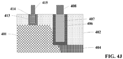
- FIG. 4A to FIG. 4J are cross-sectional views that schematically illustrate a semiconductor device at a plurality of phases of another exemplary manufacturing process of the semiconductor device.
- the initial structure may include: a semiconductor fin 401, an interlayer dielectric layer 402 covering the semiconductor fin 401 and a first dummy gate 403 located in the interlayer dielectric layer 402. An upper surface of the first dummy gate 403 flushes with an upper surface of the interlayer dielectric layer 402.
- a side surface of the semiconductor fin 401 is an inclined surface, and the first dummy gate 403 is separated from the inclined surface.
- the initial structure may further include: a trench isolation portion 404 which abuts against the inclined side surface of the semiconductor fin 401.
- the initial structure may further include: a second dummy gate 411 in the interlayer dielectric layer 402 and located on the semiconductor fin 401.
- An upper surface of the second dummy gate 411 flushes with the upper surface of the interlayer dielectric layer 402.
- material of the second dummy gate 411 may include polysilicon.
- FIG. 4A is a cross-sectional diagram. Actually, in a form, the second dummy gate 411 may transversely wraps a part of the semiconductor fin 401. For example, the dummy gate 411 may wrap around side surfaces of the semiconductor fin substantially parallel to the cross-section.
- the process of providing the initial structure shown in FIG. 4A may include: providing a first structure, where the first structure may include the semiconductor fin 401 and the trench isolation portion 404. In one implementation, the process may further include: forming the first dummy gate 403 on the trench isolation portion 404; and forming, on the semiconductor fin 401, the second dummy gate 411 wrapping a part of the semiconductor fin. In one implementation, the first dummy gate and the second dummy gate may be formed in the same process.
- the process of providing the initial structure may further include: depositing the interlayer dielectric layer 402 to cover the semiconductor fin 401, the trench isolation portion 404, the first dummy gate 403, and the second dummy gate 411.
- the process may further include: performing planarization (for example, CMP) on the interlayer dielectric layer 402, so as to expose the upper surfaces of the first dummy gate 403 and the second dummy gate 411.
- CMP planarization
- a first patterned mask layer (for example, a photo-resist) 421 is formed on the interlayer dielectric layer 402, where the first patterned mask layer 421 covers the second dummy gate 411 and exposes the first dummy gate 403.
- the first dummy gate 403 is removed by using an etching process, so as to form an opening 405.
- the opening 405 is enlarged by using an etching process (for example, isotropic dry etching process) to reach the semiconductor fin 401, so as to expose a part of the semiconductor fin 401.
- an etching process for example, isotropic dry etching process
- the first patterned mask layer 421 is removed.
- a data storage layer for example, TMO
- the data storage layer may be enabled to be formed at a bottom portion and a side surface of the opening 405.
- a conductive material layer for example, tungsten
- the conductive material layer 407 may be enabled to fill the opening 405 over the data storage layer.
- FIG. 4F the structure shown in FIG. 4E is planarized, so as to remove the data storage layer and the conductive material layer outside the opening.
- the manufacturing method may further include: forming, in the interlayer dielectric layer 402, a gate structure located on the semiconductor fin 401.
- the step of forming the gate structure may include: removing the second dummy gate 411, so as to form an open trench exposing a part of the semiconductor fin 401.
- the step of removing the second dummy gate 411 may include: as shown in FIG. 4G , forming a second patterned mask layer (for example, a photo-resist) 422 on the interlayer dielectric layer 402, where the second patterned mask layer 422 covers the data storage layer 406 and the conductive material layer 407 and exposes the second dummy gate 411.
- the step of removing the second dummy gate 411 may further include, as shown in FIG. 4H , removing the second dummy gate 411 by using an etching process, so as to form the open trench 412 exposing part of the semiconductor fin 401.
- the step of removing the second dummy gate 411 may further include: as shown in FIG. 4H , removing the second patterned mask layer 422.
- the step of forming the gate structure may further include: as shown in FIG. 4I , forming a gate structure in the open trench 412.
- the gate structure may include: a gate insulator layer 413 wrapping a part of the semiconductor fin 401 and a gate electrode 414 on the gate insulator layer 413.
- material of the gate insulator layer 413 may include a high k (dielectric constant) dielectric layer.
- Material of the gate electrode 414 may include metals such as tungsten.
- the gate electrode may further include: a work function material layer (not shown in the figures) between the gate insulator layer 413 and the gate electrode 414.
- material of the work function material layer may include: Al-Si (aluminum silicon) and/or TiN (titanium nitride).
- a conductive contact 408 may be formed on the conductive material layer 407, and a gate contact 415 may be formed on the gate electrode 414.
- materials of the conductive contact 408 and the gate contact 415 may both be tungsten.
- a method for manufacturing a semiconductor device according to another form of the present invention is provided above.
- This method may be used to manufacture a resistive memory based on the FinFET technology.
- the manufacturing method in the forms described above may help enlarge feature size during some manufacturing steps, and thus facilitates implementation of the manufacturing process and compatibility with the CMOS technology.
- the manufacturing method above does not rely on the self-aligning contact process and thus avoids difficulties associated with such a process.
- the semiconductor device may include a semiconductor fin 401 and an interlayer dielectric layer 402 covering the semiconductor fin 401.
- the interlayer dielectric layer 402 includes an opening (for example, the opening 405 of FIG. 4D exposing a part of the semiconductor fin 401.
- the semiconductor device may further include a data storage layer (for example, material of the data storage layer may include TMO) 406 in the opening of the interlayer dielectric layer.
- the data storage layer 406 may be in contact with a part of semiconductor fin 401.
- the semiconductor device may further include a conductive material layer 407 surrounded by the data storage layer 406.
- the semiconductor device according to the forms above may be used as a resistive memory.
- the semiconductor device possesses several advantages such as relaxed processing control precision, manufacturing simplicity, and compatibility with the CMOS process.
- the semiconductor device may further include: a trench isolation portion 404 which abuts against a side surface of the semiconductor fin 401.
- the data storage layer 406 is located above the trench isolation portion 404.
- a side surface of the semiconductor fin 401 may be an inclined surface, and the data storage layer 406 is in contact with the inclined surface.
- the semiconductor device may further include: a conductive contact 408 on the conductive material layer 407.
- the semiconductor device may further include: a gate structure in the interlayer dielectric layer 402 and located on the semiconductor fin 401.
- the gate structure may include: a gate insulator layer 413 wrapping a part of the semiconductor fin 401 and a gate electrode 414 on the gate insulator layer 413.
- the gate electrode may further include: a work function material layer (not shown in the figures) between the gate insulator layer 413 and the gate electrode 414.
- the semiconductor device may further include: a gate contact 415 on the gate electrode 414.
Landscapes
- Engineering & Computer Science (AREA)
- Manufacturing & Machinery (AREA)
- Semiconductor Memories (AREA)
- Insulated Gate Type Field-Effect Transistor (AREA)
Abstract
Description
- This application is based on and claims priority to Chinese Patent Application
CN201611085085.3, filed December 1, 2016 - The present invention relates to the technical field of semiconductors, particularly to a semiconductor device and a manufacturing method therefor, and more particularly to a resistive memory and a manufacturing method therefor.
- At present, RRAM (Resistive Random Access Memory) has generated much interest because this type of memory possesses several properties, such as structure simplicity, low power consumption, high operation speed, and high level of integration density. In some instances, a RRAM needs to be formed adjacent to a FinFET (Fin Field Effect Transistor).
-
FIG. 1 is a cross-sectional diagram that schematically illustrates a FinFET in the prior art and a structure of a RRAM formed adjacent to the FinFET.FIG. 1 shows a FinFET device portion and a RRAM device portion. As shown inFIG. 1 , the FinFET device may include: asemiconductor substrate 101, anupper semiconductor fin 102 on thesemiconductor substrate 101, agate insulator layer 104 on thesemiconductor fin 102, agate electrode 105 on thegate insulator layer 104, aspacer 106 at a side surface of thegate electrode 105, asource electrode 112 and a drain electrode 111 respectively at two sides of thegate electrode 105, asource contact 113 connected to thesource electrode 112, and adrain contact 114 connected to the drain electrode 111. The RRAM device may be composed of adummy gate 121, adata storage layer 122, and a fin portion, as shown in the dotted box inFIG. 1 . In addition,FIG. 1 also shows an STI (Shallow Trench Isolation) 103 and an interlayerdielectric layer 108. As shown inFIG. 1 , thedata storage layer 122 is merely formed at a small portion between the semiconductor fin and thedummy gate 121. In this way, the feature to be processed is small, leading to requirement for more precise processing control and increased manufacturing difficulties. - The drain contact 114 on the drain electrode spans the FinFET device portion and the RRAM device portion. Therefore, the
contact 114 may also be referred to as a slot contact. The RRAM inFIG. 1 may be correspondingly referred to as a SCRRAM (standing for Slot Contact RRAM). Existing investigations show that when a length Sx of an alignment portion (or overlapping portion) of theslot contact 114 and thedummy gate 121 is between 10 nm to 14 nm (i.e., an error of the length of the alignment portion is only 4 nm), better initial read current may be obtained and a better voltage may be formed. This precision of alignment calls for demanding processing control of only several nanometers. In the meanwhile, self-aligning contact process is difficult to implement. In addition, a long vertical portion of theslot contact 114, and a Γ-shaped upper portion of theslot contact 114 all lead to difficulties in the manufacturing of the slot contact. - It is an object of the present invention to provide a semiconductor device and a method for manufacturing the same by which one or more of the above discussed or other problems in the prior art may be solved,, in particular wherein the process window may provide a larger size and the semiconductor device being easier to manufacture and to be implemented. Moreover, the manufacturing method is desired to be compatible with the compatibility with the CMOS process.
- The object is achieved by the features of the respective independent claims. Further embodiments and developments are defined in the dependent claims.
- According to a first aspect of the present invention, a method for manufacturing a semiconductor device is provided, including: providing a semiconductor structure, where the semiconductor structure includes: a semiconductor fin and an interlayer dielectric layer covering the semiconductor fin, the interlayer dielectric layer having an opening exposing a first part of the semiconductor fin; forming a data storage layer at a bottom portion and a side surface of the opening; and filling a conductive material layer in the opening on the data storage layer.
- Preferably, the step of the providing a semiconductor structure includes: providing an initial structure, where the initial structure includes: a semiconductor fin, an interlayer dielectric layer covering the semiconductor fin, and a first dummy gate located in the interlayer dielectric layer, wherein an upper surface of the first dummy gate flushing with an upper surface of the interlayer dielectric layer; and removing the first dummy gate, so as to form the opening exposing the first part of the semiconductor fin.
- Preferably, the first dummy gate is separated from the semiconductor fin; and removing the first dummy gate includes: removing the first dummy gate to form an opening; and enlarging the opening by using a first etching process, so as to expose the first part of the semiconductor fin.
- Preferably, the initial structure further includes: a trench isolation portion abutting against a side surface of the semiconductor fin and the first dummy gate is located above the trench isolation portion.
- Preferably, a side surface of the semiconductor fin is an inclined surface, and the first part of the semiconductor fin exposed by the opening is within the inclined surface.
- Preferably, the data storage layer includes a transition metal oxide (TMO), for example, HfO2.
- Preferably, the method further includes: forming a conductive contact on the conductive material layer.
- Preferably, the method further includes: forming, in the interlayer dielectric layer, a gate structure located on the semiconductor fin.
- Preferably, a method for forming the gate structure includes: forming, in the interlayer dielectric layer, a second dummy gate located on the semiconductor fin, wherein an upper surface of the second dummy gate is flush with the upper surface of the interlayer dielectric layer; removing the second dummy gate, so as to form an open trench exposing a second part of the semiconductor fin; and forming a high-k metal-gate structure in the open trench.
- Preferably, before removing the first dummy gate to form the opening, the method further includes: forming a first patterned mask layer on the interlayer dielectric layer, the first mask layer covering the second dummy gate and exposing the first dummy gate; and wherein after removing the first dummy gate to form the opening and before forming the data storage layer, the method further includes: removing the first patterned mask layer.
- Preferably, forming the gate structure includes: removing the second dummy gate, so as to form an open trench exposing a part of the semiconductor fin; and forming a gate structure in the open trench.
- Preferably, the step of the removing the second dummy gate includes: forming a second patterned mask layer on the interlayer dielectric layer covering the data storage layer and the conductive material layer and exposing the second dummy gate; removing the second dummy gate using a second etching process, so as to form the open trench exposing the second part of the semiconductor fin; and removing the second patterned mask layer.
- By the manufacturing method of the present invention, the process window has a larger size and is easy to be manufactured and implemented. Moreover, the manufacturing method of the present invention has good compatibility with the CMOS process.
- According to a second aspect of the present invention, a semiconductor device is provided, including: a semiconductor fin; an interlayer dielectric layer covering the semiconductor fin, where the interlayer dielectric layer has an opening exposing a first part of the semiconductor fin; a data storage layer in the opening of the interlayer dielectric layer; and a conductive material layer filing the opening and surrounded by the data storage layer.
- Preferably, the semiconductor device further includes: a trench isolation portion abutting against a side surface of the semiconductor fin, where the data storage layer is located above the trench isolation portion.
- Preferably, the data storage layer is in contact with one side of the semiconductor fin.
- Preferably, a side surface of the semiconductor fin is an inclined surface, the first part of the semiconductor fin exposed by the opening is within the inclined surface.
- Preferably, the data storage layer here is known as TMO.
- Preferably, the semiconductor device further includes: a conductive contact on the conductive material layer.
- Preferably, the semiconductor device further includes: a gate structure in the interlayer dielectric layer and located on and wrapped-around the semiconductor fin.
- The semiconductor device according to the present invention has advantages such as large process window size and being easy to be manufactured, and has good compatibility with the CMOS process.
- According to the following detailed description of the forms for illustration purposes of the present invention with reference to the accompanying drawings, other characters and advantages of the present invention become clear.
- The accompanying drawings that form a part of the specification describe the forms of the present invention, and are used to explain the principles of the present invention together with the specification.
- With reference to the accompanying drawings, the present invention can be understood more clearly according to the following detailed description, where:
-
FIG. 1 is a cross-sectional view that schematically illustrates a FinFET and a RRAM formed adjacent to the FinFET in the prior art; -
FIG. 2 is a flowchart of a method for manufacturing a semiconductor device; -
FIG. 3A to Fig. 3F are cross-sectional views that schematically illustrate a semiconductor device at a plurality of phases of a manufacturing process; and -
FIG. 4A to FIG. 4J are cross-sectional views that schematically illustrate another semiconductor device at a plurality of phases of another manufacturing process. - Embodiments for illustration purposes of the present are described in details with reference to the accompanying drawings. It should be noted that unless being described in detail, relative layouts, mathematical expressions, and numeric values of components and steps described in these forms do not limit the present invention.
- Meanwhile, it should be noted that for ease of description, sizes of the parts shown in the accompanying drawings are not drawn according to an actual proportional relationship.
- The following exemplary forms are presented for illustration purposes only, and should not be used as any limitation on the present invention and applications or uses of the present invention.
- Technologies, methods, and devices that are known by a person of ordinary skill in the relate fields may not be discussed in detail. However, if appropriate, the technologies, methods, and devices should be considered as a part of the description.
- In all examples shown and discussed herein, any specific value should be regarded as being an example rather than a limitation. Therefore, other examples of the forms for illustration purposes may have different values.
- It should be noted that: similar reference signs, labels, numerals, and letters represent similar items in the following accompanying drawings. Therefore, once an item is defined in a figure, the item needs not to be further re-defined in subsequent figures.
-
FIG. 2 is a flowchart of an exemplary process for manufacturing a semiconductor device.FIG. 3A to FIG. 3F are cross-sectional views that schematically illustrate the semiconductor device at a plurality of phases of a manufacturing process of the semiconductor device. The exemplary manufacturing process of the semiconductor device is described in detail below with reference toFIG. 2 andFIG. 3A toFIG. 3F . - In step S201, a semiconductor structure is provided. The semiconductor structure includes: a semiconductor fin and an interlayer dielectric layer covering the semiconductor fin, where the interlayer dielectric layer has an opening exposing a part of the semiconductor fin.
- A process of providing the semiconductor structure is described in the following with reference to
FIG. 3A and FIG. 3B . In one implementation, as shown inFIG. 3A , the step of providing the semiconductor structure may include: for example, as shown inFIG. 3A , providing an initial structure. The initial structure may include: asemiconductor fin 301, aninterlayer dielectric layer 302 covering thesemiconductor fin 301, and afirst dummy gate 303 located in theinterlayer dielectric layer 302. An upper surface of thefirst dummy gate 303 flushes with an upper surface of theinterlayer dielectric layer 302. - It should be noted that the term "flush with" used in the present invention includes, but not limited to exact flushing. Instead, alignment error may be allowed. As such, the term "flush with" may include "approximately flush with" within the process control uncertainties.
- It should be noted that to avoid obscuring the concepts of the present invention,
FIG. 3A does not show details generally known in the art. For example, a source electrode, a drain electrode, or a gate insulator layer is not shown. However, according to the foregoing description, a person of ordinary skill in the art would understand how to implement the technical solution disclosed herein. - In one implementation, material of the
semiconductor fin 301 may be silicon. Thesemiconductor fin 301, for example, may be doped silicon (such as phosphorus-doped silicon). Material of theinterlayer dielectric layer 302 may be, for example, silicon dioxide. Material of the first dummy gate may be, for example, polysilicon. - In a form, as shown in
FIG. 3A , a side surface of thesemiconductor fin 301 may be an inclined surface. The first dummy gate is in contact with (as shown inFIG. 3A ) or separated from (not shown inFIG. 3A ) the inclined surface. It should be noted that the term "side surface" herein refers to a surface of various surfaces of the semiconductor fin that is in contact with a trench isolation portion (described below). - In a form, as shown in
FIG. 3A , the initial structure may further include atrench isolation portion 304 which abuts against the inclined side surface of the semiconductor fin. Thetrench isolation portion 304 may include a trench adjacent to the semiconductor fin and a trench insulator layer which at least partly fills the trench (the trench insulator layer, for example, may comprise silicon dioxide). In one implementation, thefirst dummy gate 303 is located above the trench isolation portion. - It should be noted that although
FIG. 3A shows that the first dummy gate is located above the trench isolation portion, a person of ordinary skill in the art should understand that the first dummy gate may be at other positions. For example, the first dummy gate may be above the semiconductor fin. Alternatively, part of the first dummy gate may be above the trench isolation portion, and the other part may be above the semiconductor fin. As such, the present invention is not limited hereto as to the location of the first dummy gate. - Optionally, as shown in
FIG. 3B , the step of the providing a semiconductor structure may further include: removing thefirst dummy gate 303, so as to form anopening 305 exposing a part of the semiconductor fin. For example, as shown inFIG. 3B , in a case in which thefirst dummy gate 303 is in contact with the inclined surface of thesemiconductor fin 301, thefirst dummy gate 303 is removed by using the etching process. In this way, theopening 305 exposing a part of the semiconductor fin may be directly formed. - It should be noted that although
FIG. 3B , as an example, shows that theopening 305 exposes the inclined side surface of the semiconductor fin, a person of ordinary skill in the art should understand that a position of the opening is not limited hereto. For example, the opening may be entirely located above an upper surface of the semiconductor fin rather than the inclined side surface. For another example, a part of the opening may be located above the upper surface of the semiconductor fin, and the other part may expose the inclined side surface of the semiconductor fin. - In a further alternative form, the first dummy gate is separated from the semiconductor fin. That is, the first dummy gate is not in contact with the inclined side surface or the upper surface of the semiconductor fin. In such a case, the step of forming the opening may include: removing the first dummy gate, so as to form the opening (the opening does not expose a part of the semiconductor fin yet); and enlarging the opening by using an etching process (for example, an isotropic dry etching process), so as to expose a part of the semiconductor fin. The enlargement process herein may increase feature size of the opening and provide relaxed process control precision, thereby facilitating the implementation of a subsequent filling process for the opening.
- Back to
FIG. 2 , in step S202, a data storage layer at a bottom portion and a side surface of the opening is formed. -
FIG. 3C schematically illustrates an exemplary cross-sectional view of the semiconductor device after step S202. As shown inFIG. 3C , adata storage layer 306 is formed at the bottom portion and the side surface of theopening 305. Thedata storage layer 306 may be formed, for example, by using the deposition process. In a form, thedata storage layer 306 may be a resistive functional layer used for a resistive memory. For example, material of the data storage layer may include a TMO (Transition Metal Oxide, transition metal oxide). - Back to
FIG. 2 , in step S203, a conductive material layer is formed to fill the opening on the data storage layer. -
FIG. 3D schematically illustrates a cross-sectional view of the semiconductor device after step S203. As shown inFIG. 3D , aconductive material layer 307 filling theopening 305 is formed on thedata storage layer 306 by using, for example, a deposition process. Theconductive material layer 307 may include various metals such as tungsten. - In a form, planarization, for example, CMP (Chemical Mechanical Planarization), may be performed on the structure shown in
FIG. 3D , so as to remove thedata storage layer 306 and a part of theconductive material layer 307 that is above the interlayer dielectric layer, thereby forming the structure shown inFIG. 3E . - A method for manufacturing a semiconductor device is provided above. The manufacturing method may be used to manufacture a resistive memory. Processing control precision may be relaxed, so that the manufacturing process of the semiconductor device becomes easier to implement. Further, the manufacturing method above does not rely on self-aligning contact process and thus avoid difficulties associated with such a process.
- In addition, the manufacturing method above may be implemented in the Middle-End-Of-Line (MEOL) stage during a FinFET manufacturing process. Therefore, the manufacturing method above for RRAM with FinFET is compatible with CMOS processes.
- In a form, as shown in
FIG. 3F , the method for manufacturing a semiconductor device above further includes: forming aconductive contact 308 on theconductive material layer 307. Material of the conductive contact may include, for example, metals such as tungsten. The conductive contact formed in this step is directly on the conductive material layer, and a Γ-shaped slot contact shown inFIG. 1 would be avoided. Moreover, the interlayer dielectric layer needs not to be deeply etched. Therefore, the manufacturing process of the semiconductor device becomes easier to be implemented. - In a form, the foregoing manufacturing process may further include: forming, in the interlayer dielectric layer, a gate structure located on the semiconductor fin. In one implementation, the method for forming the gate structure may include: forming, in the interlayer dielectric layer, a second dummy gate located on the semiconductor fin, where an upper surface of the second dummy gate flushes with an upper surface of the interlayer dielectric layer. In an exemplary implementation, the second dummy gate and the first dummy gate described above may be formed in the same process. The method for forming the gate structure may further include: removing the second dummy gate, so as to form an open trench exposing a part of the semiconductor fin. The method for forming the gate structure may further include: forming a gate structure in the open trench.
-
FIG. 4A to FIG. 4J are cross-sectional views that schematically illustrate a semiconductor device at a plurality of phases of another exemplary manufacturing process of the semiconductor device. - First, as shown in
FIG. 4A , an initial structure is provided. The initial structure may include: asemiconductor fin 401, aninterlayer dielectric layer 402 covering thesemiconductor fin 401 and afirst dummy gate 403 located in theinterlayer dielectric layer 402. An upper surface of thefirst dummy gate 403 flushes with an upper surface of theinterlayer dielectric layer 402. In a form, as shown inFIG. 4A , a side surface of thesemiconductor fin 401 is an inclined surface, and thefirst dummy gate 403 is separated from the inclined surface. The initial structure may further include: atrench isolation portion 404 which abuts against the inclined side surface of thesemiconductor fin 401. - In a form, as shown in
FIG. 4A , the initial structure may further include: asecond dummy gate 411 in theinterlayer dielectric layer 402 and located on thesemiconductor fin 401. An upper surface of thesecond dummy gate 411 flushes with the upper surface of theinterlayer dielectric layer 402. For example, material of thesecond dummy gate 411 may include polysilicon. It should be noted that the structure shown inFIG. 4A is a cross-sectional diagram. Actually, in a form, thesecond dummy gate 411 may transversely wraps a part of thesemiconductor fin 401. For example, thedummy gate 411 may wrap around side surfaces of the semiconductor fin substantially parallel to the cross-section. - In a form, the process of providing the initial structure shown in
FIG. 4A may include: providing a first structure, where the first structure may include thesemiconductor fin 401 and thetrench isolation portion 404. In one implementation, the process may further include: forming thefirst dummy gate 403 on thetrench isolation portion 404; and forming, on thesemiconductor fin 401, thesecond dummy gate 411 wrapping a part of the semiconductor fin. In one implementation, the first dummy gate and the second dummy gate may be formed in the same process. The process of providing the initial structure may further include: depositing theinterlayer dielectric layer 402 to cover thesemiconductor fin 401, thetrench isolation portion 404, thefirst dummy gate 403, and thesecond dummy gate 411. The process may further include: performing planarization (for example, CMP) on theinterlayer dielectric layer 402, so as to expose the upper surfaces of thefirst dummy gate 403 and thesecond dummy gate 411. - Subsequently, as shown in
FIG. 4B , a first patterned mask layer (for example, a photo-resist) 421 is formed on theinterlayer dielectric layer 402, where the first patternedmask layer 421 covers thesecond dummy gate 411 and exposes thefirst dummy gate 403. - Subsequently, as shown in
FIG. 4C , thefirst dummy gate 403 is removed by using an etching process, so as to form anopening 405. - Subsequently, as shown in
FIG. 4D , theopening 405 is enlarged by using an etching process (for example, isotropic dry etching process) to reach thesemiconductor fin 401, so as to expose a part of thesemiconductor fin 401. This may increase feature size of theopening 405 and lead to a more relaxed process control precision for implementation of the subsequent process of filling theopening 405 and forming a contact after the opening is filled (as will be described below). - Subsequently, the first patterned
mask layer 421 is removed. - Subsequently, as shown in
FIG. 4E , a data storage layer (for example, TMO) 406 is deposited, and the data storage layer may be enabled to be formed at a bottom portion and a side surface of theopening 405. Following this, a conductive material layer (for example, tungsten) 407 is deposited on thedata storage layer 406, and theconductive material layer 407 may be enabled to fill theopening 405 over the data storage layer. - Subsequently, as shown in
FIG. 4F , the structure shown inFIG. 4E is planarized, so as to remove the data storage layer and the conductive material layer outside the opening. - Subsequently, the manufacturing method may further include: forming, in the
interlayer dielectric layer 402, a gate structure located on thesemiconductor fin 401. - In one implementation, the step of forming the gate structure may include: removing the
second dummy gate 411, so as to form an open trench exposing a part of thesemiconductor fin 401. - For example, the step of removing the
second dummy gate 411 may include: as shown inFIG. 4G , forming a second patterned mask layer (for example, a photo-resist) 422 on theinterlayer dielectric layer 402, where the second patternedmask layer 422 covers thedata storage layer 406 and theconductive material layer 407 and exposes thesecond dummy gate 411. The step of removing thesecond dummy gate 411 may further include, as shown inFIG. 4H , removing thesecond dummy gate 411 by using an etching process, so as to form theopen trench 412 exposing part of thesemiconductor fin 401. The step of removing thesecond dummy gate 411 may further include: as shown inFIG. 4H , removing the second patternedmask layer 422. - Subsequently, the step of forming the gate structure may further include: as shown in
FIG. 4I , forming a gate structure in theopen trench 412. The gate structure may include: agate insulator layer 413 wrapping a part of thesemiconductor fin 401 and agate electrode 414 on thegate insulator layer 413. For example, material of thegate insulator layer 413 may include a high k (dielectric constant) dielectric layer. Material of thegate electrode 414 may include metals such as tungsten. In some forms, the gate electrode may further include: a work function material layer (not shown in the figures) between thegate insulator layer 413 and thegate electrode 414. For example, material of the work function material layer may include: Al-Si (aluminum silicon) and/or TiN (titanium nitride). - Subsequently, as shown in
FIG. 4J , aconductive contact 408 may be formed on theconductive material layer 407, and agate contact 415 may be formed on thegate electrode 414. For example, materials of theconductive contact 408 and thegate contact 415 may both be tungsten. - A method for manufacturing a semiconductor device according to another form of the present invention is provided above. This method may be used to manufacture a resistive memory based on the FinFET technology. The manufacturing method in the forms described above may help enlarge feature size during some manufacturing steps, and thus facilitates implementation of the manufacturing process and compatibility with the CMOS technology. In addition, the manufacturing method above does not rely on the self-aligning contact process and thus avoids difficulties associated with such a process.
- According to the manufacturing method of disclosed above, an exemplary semiconductor device is formed. For example, as shown in
FIG. 4J , the semiconductor device may include asemiconductor fin 401 and aninterlayer dielectric layer 402 covering thesemiconductor fin 401. Theinterlayer dielectric layer 402 includes an opening (for example, theopening 405 ofFIG. 4D exposing a part of thesemiconductor fin 401. The semiconductor device may further include a data storage layer (for example, material of the data storage layer may include TMO) 406 in the opening of the interlayer dielectric layer. Thedata storage layer 406 may be in contact with a part ofsemiconductor fin 401. The semiconductor device may further include aconductive material layer 407 surrounded by thedata storage layer 406. The semiconductor device according to the forms above may be used as a resistive memory. The semiconductor device possesses several advantages such as relaxed processing control precision, manufacturing simplicity, and compatibility with the CMOS process. - In a form, as shown in
FIG. 4J , the semiconductor device may further include: atrench isolation portion 404 which abuts against a side surface of thesemiconductor fin 401. Thedata storage layer 406 is located above thetrench isolation portion 404. - In a form, as shown in
FIG. 4J , a side surface of thesemiconductor fin 401 may be an inclined surface, and thedata storage layer 406 is in contact with the inclined surface. - In a form, as shown in
FIG. 4J , the semiconductor device may further include: aconductive contact 408 on theconductive material layer 407. - In a form, as shown in
FIG. 4J , the semiconductor device may further include: a gate structure in theinterlayer dielectric layer 402 and located on thesemiconductor fin 401. The gate structure may include: agate insulator layer 413 wrapping a part of thesemiconductor fin 401 and agate electrode 414 on thegate insulator layer 413. In some forms, the gate electrode may further include: a work function material layer (not shown in the figures) between thegate insulator layer 413 and thegate electrode 414. - In a form, as shown in
FIG. 4J , the semiconductor device may further include: agate contact 415 on thegate electrode 414. - To avoid obscuring the idea of the present invention, some details generally known in the art are not described in the forms and implementations above. According to the foregoing description, a person of ordinary skill in the art understands how to implement the technical solutions disclosed herein.
Claims (15)
- A method for manufacturing a semiconductor device, comprising:providing a semiconductor structure, wherein the semiconductor structure comprises: a semiconductor fin and an interlayer dielectric layer covering the semiconductor fin, the interlayer dielectric layer having an opening exposing a first part of the semiconductor fin;forming a data storage layer at a bottom portion and a side surface of the opening; andfilling a conductive material layer in the opening on the data storage layer.
- The method according to claim 1, wherein providing a semiconductor structure comprises:providing an initial structure, wherein the initial structure comprises: a semiconductor fin, an interlayer dielectric layer covering the semiconductor fin, and a first dummy gate located in the interlayer dielectric layer, wherein an upper surface of the first dummy gate is flush with an upper surface of the interlayer dielectric layer; andremoving the first dummy gate, so as to form the opening exposing the first part of the semiconductor fin.
- The method according to claim 2, wherein:the first dummy gate is separated from the semiconductor fin; andremoving the first dummy gate comprises:removing the first dummy gate to form an opening; andenlarging the opening by using a first etching process, so as to expose the first part of the semiconductor fin.
- The method according to claim 2 or 3, wherein:the initial structure further comprises: a trench isolation portion abutting a side surface of the semiconductor fin; andthe first dummy gate is located above the trench isolation portion.
- The method according to any one of the claims 2-4, wherein a side surface of the semiconductor fin is an inclined surface, and the first part of the semiconductor fin exposed by the opening is within the inclined surface.
- The method according to any one of the claims 2-5, further comprising forming, in the interlayer dielectric layer, a gate structure located on the semiconductor fin.
- The method according to claim 6, wherein forming the gate structure comprises:forming, in the interlayer dielectric layer, a second dummy gate located on the semiconductor fin, wherein an upper surface of the second dummy gate is flush with the upper surface of the interlayer dielectric layer;removing the second dummy gate, so as to form an open trench exposing a second part of the semiconductor fin; andforming the gate structure in the open trench.
- The method according to claim 7, whereinbefore removing the first dummy gate to form the opening, the method further comprises forming a first patterned mask layer on the interlayer dielectric layer covering the second dummy gate and exposing the first dummy gate; andwherein after removing the first dummy gate to form the opening and before forming the data storage layer, the method further comprises removing the first patterned mask layer.
- The method according to claim 7 or 8, wherein removing the second dummy gate comprises:forming a second patterned mask layer on the interlayer dielectric layer covering the data storage layer and the conductive material layer and exposing the second dummy gate;removing the second dummy gate using a second etching process, so as to form the open trench exposing the second part of the semiconductor fin; andremoving the second patterned mask layer.
- The method according to any one of the claims 1-9, wherein the data storage layer comprises a transition metal oxide, TMO.
- The method according to any one of the claims 1-10, further comprising forming a conductive contact on the conductive material layer.
- A semiconductor device, comprising:a semiconductor fin;an interlayer dielectric layer covering the semiconductor fin, wherein the interlayer dielectric layer has an opening exposing a first part of the semiconductor fin;a data storage layer in the opening of the interlayer dielectric layer; anda conductive material layer filling the opening and surrounded by the data storage layer.
- The semiconductor device according to claim 12, wherein the data storage layer is in contact with the first part of the semiconductor fin.
- The semiconductor device according to claim 12 or 13, whereina side surface of the semiconductor fin is an inclined surface, the first part of the semiconductor fin exposed by the opening is within the inclined surface; and/orthe data storage layer comprises a TMO.
- The semiconductor device according to claim 13 or 14, further comprising at least one of:a conductive contact on the conductive material layer;a gate structure in the interlayer dielectric layer and located on the semiconductor fin; anda trench isolation portion abutting a side surface of the semiconductor fin, wherein the data storage layer is located above the trench isolation portion.
Applications Claiming Priority (1)
| Application Number | Priority Date | Filing Date | Title |
|---|---|---|---|
| CN201611085085.3A CN108133946B (en) | 2016-12-01 | 2016-12-01 | Semiconductor device and method for manufacturing the same |
Publications (2)
| Publication Number | Publication Date |
|---|---|
| EP3331037A1 true EP3331037A1 (en) | 2018-06-06 |
| EP3331037B1 EP3331037B1 (en) | 2021-01-27 |
Family
ID=60515173
Family Applications (1)
| Application Number | Title | Priority Date | Filing Date |
|---|---|---|---|
| EP17204257.4A Active EP3331037B1 (en) | 2016-12-01 | 2017-11-29 | Semiconductor device and manufacturing method therefor |
Country Status (3)
| Country | Link |
|---|---|
| US (2) | US10522651B2 (en) |
| EP (1) | EP3331037B1 (en) |
| CN (1) | CN108133946B (en) |
Families Citing this family (5)
| Publication number | Priority date | Publication date | Assignee | Title |
|---|---|---|---|---|
| US10580977B2 (en) * | 2018-07-24 | 2020-03-03 | International Business Machines Corporation | Tightly integrated 1T1R ReRAM for planar technology |
| US10879311B2 (en) | 2019-02-08 | 2020-12-29 | International Business Machines Corporation | Vertical transport Fin field effect transistors combined with resistive memory structures |
| US11856801B2 (en) * | 2020-06-16 | 2023-12-26 | Taiwan Semiconductor Manufacturing Company Limited | Threshold voltage-modulated memory device using variable-capacitance and methods of forming the same |
| CN113950190B (en) * | 2020-07-15 | 2025-01-24 | 欣兴电子股份有限公司 | Embedded component structure and manufacturing method thereof |
| CN114649331B (en) * | 2020-12-21 | 2026-03-06 | 中芯国际集成电路制造(上海)有限公司 | Semiconductor structure and its formation method |
Citations (4)
| Publication number | Priority date | Publication date | Assignee | Title |
|---|---|---|---|---|
| EP2202816A1 (en) * | 2008-12-24 | 2010-06-30 | Imec | Method for manufacturing a resistive switching memory device and devices obtained thereof |
| US20130148409A1 (en) * | 2011-02-14 | 2013-06-13 | Shine C. Chung | Circuit and system of using finfet for building programmable resistive devices |
| US20150325626A1 (en) * | 2014-05-08 | 2015-11-12 | Chrong-Jung Lin | Non-volatile memory with resistive element and manufacturing method thereof |
| US20160172445A1 (en) * | 2014-12-15 | 2016-06-16 | Sang U Kim | Finfet transistor |
Family Cites Families (14)
| Publication number | Priority date | Publication date | Assignee | Title |
|---|---|---|---|---|
| US4650544A (en) * | 1985-04-19 | 1987-03-17 | Advanced Micro Devices, Inc. | Shallow groove capacitor fabrication method |
| US5595926A (en) * | 1994-06-29 | 1997-01-21 | Industrial Technology Research Institute | Method for fabricating a DRAM trench capacitor with recessed pillar |
| US6963103B2 (en) * | 2001-08-30 | 2005-11-08 | Micron Technology, Inc. | SRAM cells with repressed floating gate memory, low tunnel barrier interpoly insulators |
| US6710391B2 (en) * | 2002-06-26 | 2004-03-23 | Texas Instruments Incorporated | Integrated DRAM process/structure using contact pillars |
| KR100621628B1 (en) * | 2004-05-31 | 2006-09-19 | 삼성전자주식회사 | Nonvolatile Memory Cells and Their Formation Methods |
| CN100508167C (en) * | 2004-11-30 | 2009-07-01 | 富士通微电子株式会社 | Semiconductor memory device and method of manufacturing the same |
| US7859081B2 (en) * | 2007-03-29 | 2010-12-28 | Intel Corporation | Capacitor, method of increasing a capacitance area of same, and system containing same |
| US7776684B2 (en) * | 2007-03-30 | 2010-08-17 | Intel Corporation | Increasing the surface area of a memory cell capacitor |
| JP2009140970A (en) * | 2007-12-03 | 2009-06-25 | Elpida Memory Inc | Semiconductor device and manufacturing method of semiconductor device |
| US8258564B2 (en) * | 2008-04-17 | 2012-09-04 | Qimonda Ag | Integrated circuit with floating-gate electrodes including a transition metal and corresponding manufacturing method |
| KR101548674B1 (en) * | 2009-08-26 | 2015-09-01 | 삼성전자주식회사 | Three-dimensional semiconductor memory device and manufacturing method thereof |
| JP5549105B2 (en) * | 2009-04-15 | 2014-07-16 | ソニー株式会社 | Resistance change type memory device and operation method thereof |
| JP2010251529A (en) * | 2009-04-16 | 2010-11-04 | Sony Corp | Semiconductor memory device and manufacturing method thereof |
| KR20170000134A (en) * | 2015-06-23 | 2017-01-02 | 삼성전자주식회사 | Semiconductor device and method for fabricating the same |
-
2016
- 2016-12-01 CN CN201611085085.3A patent/CN108133946B/en active Active
-
2017
- 2017-11-27 US US15/823,029 patent/US10522651B2/en active Active
- 2017-11-29 EP EP17204257.4A patent/EP3331037B1/en active Active
-
2019
- 2019-12-03 US US16/701,994 patent/US11069792B2/en active Active
Patent Citations (4)
| Publication number | Priority date | Publication date | Assignee | Title |
|---|---|---|---|---|
| EP2202816A1 (en) * | 2008-12-24 | 2010-06-30 | Imec | Method for manufacturing a resistive switching memory device and devices obtained thereof |
| US20130148409A1 (en) * | 2011-02-14 | 2013-06-13 | Shine C. Chung | Circuit and system of using finfet for building programmable resistive devices |
| US20150325626A1 (en) * | 2014-05-08 | 2015-11-12 | Chrong-Jung Lin | Non-volatile memory with resistive element and manufacturing method thereof |
| US20160172445A1 (en) * | 2014-12-15 | 2016-06-16 | Sang U Kim | Finfet transistor |
Also Published As
| Publication number | Publication date |
|---|---|
| US20180158928A1 (en) | 2018-06-07 |
| US11069792B2 (en) | 2021-07-20 |
| CN108133946B (en) | 2020-10-16 |
| EP3331037B1 (en) | 2021-01-27 |
| CN108133946A (en) | 2018-06-08 |
| US10522651B2 (en) | 2019-12-31 |
| US20200105907A1 (en) | 2020-04-02 |
Similar Documents
| Publication | Publication Date | Title |
|---|---|---|
| US11069792B2 (en) | Semiconductor device and manufacturing method therefor | |
| CN104637819B (en) | The replacement gate structure and the method and device of fin formed on FinFET devices | |
| US10236290B2 (en) | Method and structure for improving vertical transistor | |
| KR102287271B1 (en) | Non-planar semiconductor device having omega-fin with doped sub-fin region and method to fabricate same | |
| CN104517859B (en) | The method and device of fin field-effect transistor are formed using replacement gate technique | |
| CN107680968B (en) | Method of Integrating Multiple Gate Dielectric Transistors on Tri-Gate (FINFET) Process | |
| US10468257B2 (en) | Mechanisms for semiconductor device structure | |
| US9882023B2 (en) | Sidewall spacers for self-aligned contacts | |
| CN107170825A (en) | Semiconductor device with a plurality of transistors | |
| TW201513231A (en) | Method for forming a replacement gate structure of a transistor and finished device thereof | |
| CN105762108A (en) | Semiconductor structure and formation method thereof | |
| US8802521B1 (en) | Semiconductor fin-shaped structure and manufacturing process thereof | |
| KR102302073B1 (en) | A semiconductor device and methods of manufacturing the same | |
| CN106683990A (en) | Semiconductor element and manufacturing method thereof | |
| KR102311552B1 (en) | Semiconductor device and method for manufacturing of the same | |
| US9412759B2 (en) | CMOS gate contact resistance reduction | |
| US20190341426A1 (en) | Resistive memory and method for fabricating the same and applications thereof | |
| CN105280709A (en) | Methods of forming a nanowire device with a gate-all-around-channel configuration and the resulting nanowire device | |
| TWI848509B (en) | Memory device and methods of forming the same | |
| US9978873B2 (en) | Method for fabricating FinFet | |
| TWI758995B (en) | Memory device and methods of forming | |
| CN112447718B (en) | Semiconductor structure, preparation method and dynamic random access memory | |
| US10651174B2 (en) | FinFET structure and fabricating method of gate structure | |
| TWI713202B (en) | Flash memories and methods for forming the same | |
| CN114068396B (en) | Semiconductor structure and forming method thereof |
Legal Events
| Date | Code | Title | Description |
|---|---|---|---|
| PUAI | Public reference made under article 153(3) epc to a published international application that has entered the european phase |
Free format text: ORIGINAL CODE: 0009012 |
|
| STAA | Information on the status of an ep patent application or granted ep patent |
Free format text: STATUS: THE APPLICATION HAS BEEN PUBLISHED |
|
| AK | Designated contracting states |
Kind code of ref document: A1 Designated state(s): AL AT BE BG CH CY CZ DE DK EE ES FI FR GB GR HR HU IE IS IT LI LT LU LV MC MK MT NL NO PL PT RO RS SE SI SK SM TR |
|
| AX | Request for extension of the european patent |
Extension state: BA ME |
|
| RAP1 | Party data changed (applicant data changed or rights of an application transferred) |
Owner name: SEMICONDUCTOR MANUFACTURING INTERNATIONAL (SHANGHA Owner name: SEMICONDUCTOR MANUFACTURING INTERNATIONAL (BEIJING |
|
| STAA | Information on the status of an ep patent application or granted ep patent |
Free format text: STATUS: REQUEST FOR EXAMINATION WAS MADE |
|
| 17P | Request for examination filed |
Effective date: 20181206 |
|
| RBV | Designated contracting states (corrected) |
Designated state(s): AL AT BE BG CH CY CZ DE DK EE ES FI FR GB GR HR HU IE IS IT LI LT LU LV MC MK MT NL NO PL PT RO RS SE SI SK SM TR |
|
| GRAP | Despatch of communication of intention to grant a patent |
Free format text: ORIGINAL CODE: EPIDOSNIGR1 |
|
| STAA | Information on the status of an ep patent application or granted ep patent |
Free format text: STATUS: GRANT OF PATENT IS INTENDED |
|
| INTG | Intention to grant announced |
Effective date: 20200825 |
|
| GRAS | Grant fee paid |
Free format text: ORIGINAL CODE: EPIDOSNIGR3 |
|
| GRAA | (expected) grant |
Free format text: ORIGINAL CODE: 0009210 |
|
| STAA | Information on the status of an ep patent application or granted ep patent |
Free format text: STATUS: THE PATENT HAS BEEN GRANTED |
|
| AK | Designated contracting states |
Kind code of ref document: B1 Designated state(s): AL AT BE BG CH CY CZ DE DK EE ES FI FR GB GR HR HU IE IS IT LI LT LU LV MC MK MT NL NO PL PT RO RS SE SI SK SM TR |
|
| REG | Reference to a national code |
Ref country code: GB Ref legal event code: FG4D |
|
| REG | Reference to a national code |
Ref country code: CH Ref legal event code: EP |
|
| REG | Reference to a national code |
Ref country code: AT Ref legal event code: REF Ref document number: 1359147 Country of ref document: AT Kind code of ref document: T Effective date: 20210215 |
|
| REG | Reference to a national code |
Ref country code: IE Ref legal event code: FG4D |
|
| REG | Reference to a national code |
Ref country code: DE Ref legal event code: R096 Ref document number: 602017031992 Country of ref document: DE |
|
| REG | Reference to a national code |
Ref country code: NL Ref legal event code: MP Effective date: 20210127 |
|
| REG | Reference to a national code |
Ref country code: LT Ref legal event code: MG9D |
|
| REG | Reference to a national code |
Ref country code: AT Ref legal event code: MK05 Ref document number: 1359147 Country of ref document: AT Kind code of ref document: T Effective date: 20210127 |
|
| PG25 | Lapsed in a contracting state [announced via postgrant information from national office to epo] |
Ref country code: PT Free format text: LAPSE BECAUSE OF FAILURE TO SUBMIT A TRANSLATION OF THE DESCRIPTION OR TO PAY THE FEE WITHIN THE PRESCRIBED TIME-LIMIT Effective date: 20210527 Ref country code: NO Free format text: LAPSE BECAUSE OF FAILURE TO SUBMIT A TRANSLATION OF THE DESCRIPTION OR TO PAY THE FEE WITHIN THE PRESCRIBED TIME-LIMIT Effective date: 20210427 Ref country code: HR Free format text: LAPSE BECAUSE OF FAILURE TO SUBMIT A TRANSLATION OF THE DESCRIPTION OR TO PAY THE FEE WITHIN THE PRESCRIBED TIME-LIMIT Effective date: 20210127 Ref country code: FI Free format text: LAPSE BECAUSE OF FAILURE TO SUBMIT A TRANSLATION OF THE DESCRIPTION OR TO PAY THE FEE WITHIN THE PRESCRIBED TIME-LIMIT Effective date: 20210127 Ref country code: GR Free format text: LAPSE BECAUSE OF FAILURE TO SUBMIT A TRANSLATION OF THE DESCRIPTION OR TO PAY THE FEE WITHIN THE PRESCRIBED TIME-LIMIT Effective date: 20210428 Ref country code: BG Free format text: LAPSE BECAUSE OF FAILURE TO SUBMIT A TRANSLATION OF THE DESCRIPTION OR TO PAY THE FEE WITHIN THE PRESCRIBED TIME-LIMIT Effective date: 20210427 Ref country code: LT Free format text: LAPSE BECAUSE OF FAILURE TO SUBMIT A TRANSLATION OF THE DESCRIPTION OR TO PAY THE FEE WITHIN THE PRESCRIBED TIME-LIMIT Effective date: 20210127 |
|
| PG25 | Lapsed in a contracting state [announced via postgrant information from national office to epo] |
Ref country code: RS Free format text: LAPSE BECAUSE OF FAILURE TO SUBMIT A TRANSLATION OF THE DESCRIPTION OR TO PAY THE FEE WITHIN THE PRESCRIBED TIME-LIMIT Effective date: 20210127 Ref country code: LV Free format text: LAPSE BECAUSE OF FAILURE TO SUBMIT A TRANSLATION OF THE DESCRIPTION OR TO PAY THE FEE WITHIN THE PRESCRIBED TIME-LIMIT Effective date: 20210127 Ref country code: PL Free format text: LAPSE BECAUSE OF FAILURE TO SUBMIT A TRANSLATION OF THE DESCRIPTION OR TO PAY THE FEE WITHIN THE PRESCRIBED TIME-LIMIT Effective date: 20210127 Ref country code: AT Free format text: LAPSE BECAUSE OF FAILURE TO SUBMIT A TRANSLATION OF THE DESCRIPTION OR TO PAY THE FEE WITHIN THE PRESCRIBED TIME-LIMIT Effective date: 20210127 Ref country code: SE Free format text: LAPSE BECAUSE OF FAILURE TO SUBMIT A TRANSLATION OF THE DESCRIPTION OR TO PAY THE FEE WITHIN THE PRESCRIBED TIME-LIMIT Effective date: 20210127 |
|
| PG25 | Lapsed in a contracting state [announced via postgrant information from national office to epo] |
Ref country code: IS Free format text: LAPSE BECAUSE OF FAILURE TO SUBMIT A TRANSLATION OF THE DESCRIPTION OR TO PAY THE FEE WITHIN THE PRESCRIBED TIME-LIMIT Effective date: 20210527 |
|
| REG | Reference to a national code |
Ref country code: DE Ref legal event code: R097 Ref document number: 602017031992 Country of ref document: DE |
|
| PG25 | Lapsed in a contracting state [announced via postgrant information from national office to epo] |
Ref country code: EE Free format text: LAPSE BECAUSE OF FAILURE TO SUBMIT A TRANSLATION OF THE DESCRIPTION OR TO PAY THE FEE WITHIN THE PRESCRIBED TIME-LIMIT Effective date: 20210127 Ref country code: CZ Free format text: LAPSE BECAUSE OF FAILURE TO SUBMIT A TRANSLATION OF THE DESCRIPTION OR TO PAY THE FEE WITHIN THE PRESCRIBED TIME-LIMIT Effective date: 20210127 Ref country code: SM Free format text: LAPSE BECAUSE OF FAILURE TO SUBMIT A TRANSLATION OF THE DESCRIPTION OR TO PAY THE FEE WITHIN THE PRESCRIBED TIME-LIMIT Effective date: 20210127 |
|
| PG25 | Lapsed in a contracting state [announced via postgrant information from national office to epo] |
Ref country code: SK Free format text: LAPSE BECAUSE OF FAILURE TO SUBMIT A TRANSLATION OF THE DESCRIPTION OR TO PAY THE FEE WITHIN THE PRESCRIBED TIME-LIMIT Effective date: 20210127 Ref country code: RO Free format text: LAPSE BECAUSE OF FAILURE TO SUBMIT A TRANSLATION OF THE DESCRIPTION OR TO PAY THE FEE WITHIN THE PRESCRIBED TIME-LIMIT Effective date: 20210127 Ref country code: DK Free format text: LAPSE BECAUSE OF FAILURE TO SUBMIT A TRANSLATION OF THE DESCRIPTION OR TO PAY THE FEE WITHIN THE PRESCRIBED TIME-LIMIT Effective date: 20210127 |
|
| PLBE | No opposition filed within time limit |
Free format text: ORIGINAL CODE: 0009261 |
|
| STAA | Information on the status of an ep patent application or granted ep patent |
Free format text: STATUS: NO OPPOSITION FILED WITHIN TIME LIMIT |
|
| 26N | No opposition filed |
Effective date: 20211028 |
|
| PG25 | Lapsed in a contracting state [announced via postgrant information from national office to epo] |
Ref country code: ES Free format text: LAPSE BECAUSE OF FAILURE TO SUBMIT A TRANSLATION OF THE DESCRIPTION OR TO PAY THE FEE WITHIN THE PRESCRIBED TIME-LIMIT Effective date: 20210127 Ref country code: AL Free format text: LAPSE BECAUSE OF FAILURE TO SUBMIT A TRANSLATION OF THE DESCRIPTION OR TO PAY THE FEE WITHIN THE PRESCRIBED TIME-LIMIT Effective date: 20210127 |
|
| PG25 | Lapsed in a contracting state [announced via postgrant information from national office to epo] |
Ref country code: SI Free format text: LAPSE BECAUSE OF FAILURE TO SUBMIT A TRANSLATION OF THE DESCRIPTION OR TO PAY THE FEE WITHIN THE PRESCRIBED TIME-LIMIT Effective date: 20210127 |
|
| PG25 | Lapsed in a contracting state [announced via postgrant information from national office to epo] |
Ref country code: IT Free format text: LAPSE BECAUSE OF FAILURE TO SUBMIT A TRANSLATION OF THE DESCRIPTION OR TO PAY THE FEE WITHIN THE PRESCRIBED TIME-LIMIT Effective date: 20210127 |
|
| PG25 | Lapsed in a contracting state [announced via postgrant information from national office to epo] |
Ref country code: IS Free format text: LAPSE BECAUSE OF FAILURE TO SUBMIT A TRANSLATION OF THE DESCRIPTION OR TO PAY THE FEE WITHIN THE PRESCRIBED TIME-LIMIT Effective date: 20210527 |
|
| PG25 | Lapsed in a contracting state [announced via postgrant information from national office to epo] |
Ref country code: MC Free format text: LAPSE BECAUSE OF FAILURE TO SUBMIT A TRANSLATION OF THE DESCRIPTION OR TO PAY THE FEE WITHIN THE PRESCRIBED TIME-LIMIT Effective date: 20210127 |
|
| REG | Reference to a national code |
Ref country code: CH Ref legal event code: PL |
|
| GBPC | Gb: european patent ceased through non-payment of renewal fee |
Effective date: 20211129 |
|
| PG25 | Lapsed in a contracting state [announced via postgrant information from national office to epo] |
Ref country code: LU Free format text: LAPSE BECAUSE OF NON-PAYMENT OF DUE FEES Effective date: 20211129 Ref country code: BE Free format text: LAPSE BECAUSE OF NON-PAYMENT OF DUE FEES Effective date: 20211130 |
|
| REG | Reference to a national code |
Ref country code: BE Ref legal event code: MM Effective date: 20211130 |
|
| PG25 | Lapsed in a contracting state [announced via postgrant information from national office to epo] |
Ref country code: IE Free format text: LAPSE BECAUSE OF NON-PAYMENT OF DUE FEES Effective date: 20211129 Ref country code: GB Free format text: LAPSE BECAUSE OF NON-PAYMENT OF DUE FEES Effective date: 20211129 |
|
| REG | Reference to a national code |
Ref country code: DE Ref legal event code: R079 Ref document number: 602017031992 Country of ref document: DE Free format text: PREVIOUS MAIN CLASS: H01L0045000000 Ipc: H10N0070000000 |
|
| PG25 | Lapsed in a contracting state [announced via postgrant information from national office to epo] |
Ref country code: FR Free format text: LAPSE BECAUSE OF NON-PAYMENT OF DUE FEES Effective date: 20211130 |
|
| PG25 | Lapsed in a contracting state [announced via postgrant information from national office to epo] |
Ref country code: HU Free format text: LAPSE BECAUSE OF FAILURE TO SUBMIT A TRANSLATION OF THE DESCRIPTION OR TO PAY THE FEE WITHIN THE PRESCRIBED TIME-LIMIT; INVALID AB INITIO Effective date: 20171129 |
|
| PG25 | Lapsed in a contracting state [announced via postgrant information from national office to epo] |
Ref country code: NL Free format text: LAPSE BECAUSE OF NON-PAYMENT OF DUE FEES Effective date: 20210127 Ref country code: CY Free format text: LAPSE BECAUSE OF FAILURE TO SUBMIT A TRANSLATION OF THE DESCRIPTION OR TO PAY THE FEE WITHIN THE PRESCRIBED TIME-LIMIT Effective date: 20210127 |
|
| PG25 | Lapsed in a contracting state [announced via postgrant information from national office to epo] |
Ref country code: LI Free format text: LAPSE BECAUSE OF NON-PAYMENT OF DUE FEES Effective date: 20220630 Ref country code: CH Free format text: LAPSE BECAUSE OF NON-PAYMENT OF DUE FEES Effective date: 20220630 |
|
| PG25 | Lapsed in a contracting state [announced via postgrant information from national office to epo] |
Ref country code: MK Free format text: LAPSE BECAUSE OF FAILURE TO SUBMIT A TRANSLATION OF THE DESCRIPTION OR TO PAY THE FEE WITHIN THE PRESCRIBED TIME-LIMIT Effective date: 20210127 |
|
| PG25 | Lapsed in a contracting state [announced via postgrant information from national office to epo] |
Ref country code: MT Free format text: LAPSE BECAUSE OF FAILURE TO SUBMIT A TRANSLATION OF THE DESCRIPTION OR TO PAY THE FEE WITHIN THE PRESCRIBED TIME-LIMIT Effective date: 20210127 |
|
| PG25 | Lapsed in a contracting state [announced via postgrant information from national office to epo] |
Ref country code: TR Free format text: LAPSE BECAUSE OF FAILURE TO SUBMIT A TRANSLATION OF THE DESCRIPTION OR TO PAY THE FEE WITHIN THE PRESCRIBED TIME-LIMIT Effective date: 20210127 |
|
| PGFP | Annual fee paid to national office [announced via postgrant information from national office to epo] |
Ref country code: DE Payment date: 20251119 Year of fee payment: 9 |