US9412759B2 - CMOS gate contact resistance reduction - Google Patents
CMOS gate contact resistance reduction Download PDFInfo
- Publication number
- US9412759B2 US9412759B2 US14/566,779 US201414566779A US9412759B2 US 9412759 B2 US9412759 B2 US 9412759B2 US 201414566779 A US201414566779 A US 201414566779A US 9412759 B2 US9412759 B2 US 9412759B2
- Authority
- US
- United States
- Prior art keywords
- gate
- contact
- layer
- portions
- dielectric
- Prior art date
- Legal status (The legal status is an assumption and is not a legal conclusion. Google has not performed a legal analysis and makes no representation as to the accuracy of the status listed.)
- Active
Links
Images


Classifications
-
- H01L27/1211—
-
- H—ELECTRICITY
- H10—SEMICONDUCTOR DEVICES; ELECTRIC SOLID-STATE DEVICES NOT OTHERWISE PROVIDED FOR
- H10D—INORGANIC ELECTRIC SEMICONDUCTOR DEVICES
- H10D86/00—Integrated devices formed in or on insulating or conducting substrates, e.g. formed in silicon-on-insulator [SOI] substrates or on stainless steel or glass substrates
- H10D86/201—Integrated devices formed in or on insulating or conducting substrates, e.g. formed in silicon-on-insulator [SOI] substrates or on stainless steel or glass substrates the substrates comprising an insulating layer on a semiconductor body, e.g. SOI
- H10D86/215—Integrated devices formed in or on insulating or conducting substrates, e.g. formed in silicon-on-insulator [SOI] substrates or on stainless steel or glass substrates the substrates comprising an insulating layer on a semiconductor body, e.g. SOI comprising FinFETs
-
- H01L21/28017—
-
- H01L21/31111—
-
- H01L21/845—
-
- H01L29/0649—
-
- H01L29/42364—
-
- H01L29/42376—
-
- H01L29/6653—
-
- H—ELECTRICITY
- H10—SEMICONDUCTOR DEVICES; ELECTRIC SOLID-STATE DEVICES NOT OTHERWISE PROVIDED FOR
- H10D—INORGANIC ELECTRIC SEMICONDUCTOR DEVICES
- H10D62/00—Semiconductor bodies, or regions thereof, of devices having potential barriers
- H10D62/10—Shapes, relative sizes or dispositions of the regions of the semiconductor bodies; Shapes of the semiconductor bodies
- H10D62/113—Isolations within a component, i.e. internal isolations
- H10D62/115—Dielectric isolations, e.g. air gaps
-
- H—ELECTRICITY
- H10—SEMICONDUCTOR DEVICES; ELECTRIC SOLID-STATE DEVICES NOT OTHERWISE PROVIDED FOR
- H10D—INORGANIC ELECTRIC SEMICONDUCTOR DEVICES
- H10D64/00—Electrodes of devices having potential barriers
- H10D64/01—Manufacture or treatment
- H10D64/013—Manufacture or treatment of electrodes having a conductor capacitively coupled to a semiconductor by an insulator
- H10D64/01302—Manufacture or treatment of electrodes having a conductor capacitively coupled to a semiconductor by an insulator the insulator being formed after the semiconductor body, the semiconductor being silicon
-
- H—ELECTRICITY
- H10—SEMICONDUCTOR DEVICES; ELECTRIC SOLID-STATE DEVICES NOT OTHERWISE PROVIDED FOR
- H10D—INORGANIC ELECTRIC SEMICONDUCTOR DEVICES
- H10D64/00—Electrodes of devices having potential barriers
- H10D64/01—Manufacture or treatment
- H10D64/015—Manufacture or treatment removing at least parts of gate spacers, e.g. disposable spacers
-
- H—ELECTRICITY
- H10—SEMICONDUCTOR DEVICES; ELECTRIC SOLID-STATE DEVICES NOT OTHERWISE PROVIDED FOR
- H10D—INORGANIC ELECTRIC SEMICONDUCTOR DEVICES
- H10D64/00—Electrodes of devices having potential barriers
- H10D64/20—Electrodes characterised by their shapes, relative sizes or dispositions
- H10D64/27—Electrodes not carrying the current to be rectified, amplified, oscillated or switched, e.g. gates
- H10D64/311—Gate electrodes for field-effect devices
- H10D64/411—Gate electrodes for field-effect devices for FETs
- H10D64/511—Gate electrodes for field-effect devices for FETs for IGFETs
- H10D64/514—Gate electrodes for field-effect devices for FETs for IGFETs characterised by the insulating layers
-
- H—ELECTRICITY
- H10—SEMICONDUCTOR DEVICES; ELECTRIC SOLID-STATE DEVICES NOT OTHERWISE PROVIDED FOR
- H10D—INORGANIC ELECTRIC SEMICONDUCTOR DEVICES
- H10D64/00—Electrodes of devices having potential barriers
- H10D64/20—Electrodes characterised by their shapes, relative sizes or dispositions
- H10D64/27—Electrodes not carrying the current to be rectified, amplified, oscillated or switched, e.g. gates
- H10D64/311—Gate electrodes for field-effect devices
- H10D64/411—Gate electrodes for field-effect devices for FETs
- H10D64/511—Gate electrodes for field-effect devices for FETs for IGFETs
- H10D64/517—Gate electrodes for field-effect devices for FETs for IGFETs characterised by the conducting layers
- H10D64/518—Gate electrodes for field-effect devices for FETs for IGFETs characterised by the conducting layers characterised by their lengths or sectional shapes
-
- H—ELECTRICITY
- H10—SEMICONDUCTOR DEVICES; ELECTRIC SOLID-STATE DEVICES NOT OTHERWISE PROVIDED FOR
- H10D—INORGANIC ELECTRIC SEMICONDUCTOR DEVICES
- H10D86/00—Integrated devices formed in or on insulating or conducting substrates, e.g. formed in silicon-on-insulator [SOI] substrates or on stainless steel or glass substrates
- H10D86/01—Manufacture or treatment
- H10D86/011—Manufacture or treatment comprising FinFETs
Definitions
- the present application relates to the fabrication of semiconductor devices, and more particularly, to the formation of gate contacts with reduced contact resistance.
- FETs Field Effect Transistors
- a FET device includes a source, a drain and a channel region between the source and the drain.
- a gate electrode over the channel region regulates electron flow between the source and the drain.
- a gate contact typically contacts a top surface of the gate electrode to electrically connect the gate electrode to other active components in integrated circuits.
- the gate contact area may be relatively small.
- a small gate contact area can lead to high gate contact resistance, which in turn degrades FET frequency response and performance. As such, there remains a need to increase gate contact area.
- the present application provides gate contacts with increased gate contact area by removing at least portions of a gate dielectric portion present on sidewalls of a portion of a gate conductive portion of a gate structure.
- the gate contact forms a direct contact with a topmost surface and at least portions of outermost sidewalls of the gate conductive portion, thus increasing the contact area between the gate contact and the gate structure.
- the increased gate contact area reduces gate contact resistance, thus increasing the device performance.
- the gate contact area of the present application can be further increased by completely surrounding a portion of the gate conductive portion of the gate structure with the gate contact.
- a semiconductor structure in one aspect of the present application, includes a substrate comprising a first device region and a second device region separated from one another by an insulating region, and at least one gate structure overlying at least one channel portion of each of the first device region and the second device region.
- the at least one gate structure comprises a gate spacer, a U-shaped gate dielectric laterally surrounded by the gate spacer, and a gate conductive portion in contact with the U-shaped gate dielectric.
- the semiconductor structure further includes a gate contact contacting a portion of the at least one gate structure located in the insulating region. The gate contact is in direct contact with a topmost surface and at least portions of outermost sidewalls of the gate conductive portion.
- a method of forming a semiconductor structure includes forming at least one gate structure on a substrate comprising a first device region and a second device region separated from one another by an insulating region.
- the at least one gate structure overlies at least one channel portion of each of the first device region and the second device region and includes a gate spacer, a U-shaped gate dielectric laterally surrounded by the gate spacer, and a gate conductive portion in contact with the U-shaped gate dielectric.
- a gate contact trench is then formed through a contact level dielectric layer and at least a portion of an interlevel dielectric (ILD) layer underlying the contact level dielectric layer.
- ILD interlevel dielectric
- the gate contact trench exposes a topmost surface and at least portions of outermost sidewalls of the gate conductive portion in a portion of the at least one gate structure located in the insulating region of the substrate.
- a gate contact is formed within the gate contact trench. The gate contact is in contact with the topmost surface and the at least portions of the outermost sidewalls of the gate conductive portion located within the gate contact trench.
- a method of forming a semiconductor structure includes forming at least one gate structure on a substrate comprising a first device region and a second device region separated from one another by an insulating region.
- the at least one gate structure overlies at least one channel portion of each of the first device region and the second device region and comprises a gate spacer, a U-shaped gate dielectric laterally surrounded by the gate spacer, and a gate conductive portion in contact with the U-shaped gate dielectric.
- a gate contact trench is formed through a contact level dielectric layer, an ILD layer and into an upper portion of a buried insulator layer of the substrate located underneath the first device region and the second device region.
- the buried insulator layer provides the insulating region.
- the gate contact trench exposes an entirety of a portion of the gate conductive portion of the at least one gate structure located in the insulating region of the substrate.
- a gate contact is formed within the gate contact trench. The gate contact is in contact with the entirety of the gate conductive portion located within the gate contact trench.
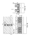
- FIG. 1A is a top view of an exemplary semiconductor structure including an array of first semiconductor fins and an array of second semiconductor fins formed on a substrate in accordance with an embodiment of present application.
- FIG. 1B is a cross-sectional view of the exemplary semiconductor structure of FIG. 1A along line B-B′.
- FIG. 1C is a cross-sectional view of the exemplary semiconductor structure of FIG. 1A along line C-C′.
- FIG. 2A is a top view of the exemplary semiconductor structure of FIGS. 1A-1C after forming sacrificial gate structures over a channel portion of each of the first semiconductor fins and the second semiconductor fins.
- FIG. 2B is a cross-sectional view of the exemplary semiconductor structure of FIG. 2A along line B-B′.
- FIG. 2C is a cross-sectional view of the exemplary semiconductor structure of FIG. 2A along line C-C′.
- FIG. 3A is a top view of the exemplary semiconductor structure of FIGS. 2A-2C after forming an interlevel dielectric (ILD) layer over the substrate to laterally surround the sacrificial gate structures.
- ILD interlevel dielectric
- FIG. 3B is a cross-sectional view of the exemplary semiconductor structure of FIG. 3A along line B-B′.
- FIG. 3C is a cross-sectional view of the exemplary semiconductor structure of FIG. 3A along line C-C′.
- FIG. 4A is a top view of the exemplary semiconductor structure of FIGS. 3A-3C after forming gate cavities.
- FIG. 4B is a cross-sectional view of the exemplary semiconductor structure of FIG. 4A along line B-B′.
- FIG. 4C is a cross-sectional view of the exemplary semiconductor structure of FIG. 4A along line C-C′.
- FIG. 5B is a cross-sectional view of the exemplary semiconductor structure of FIG. 5A along line B-B′.
- FIG. 5C is a cross-sectional view of the exemplary semiconductor structure of FIG. 5A along line C-C′.
- FIG. 6A is a top view of the exemplary semiconductor structure of FIGS. 5A-5C after forming a contact level dielectric over the ILD layer and the functional gate structures.
- FIG. 6B is a cross-sectional view of the exemplary semiconductor structure of FIG. 6A along line B-B′.
- FIG. 6C is a cross-sectional view of the exemplary semiconductor structure of FIG. 6A along line C-C′.
- FIG. 7A is a top view of a first exemplary semiconductor structure that can be derived from the exemplary semiconductor structure of FIGS. 6A-6C after forming a gate contact trench to expose topmost surfaces and portions of outermost sidewalls of a portion of a gate conductive portion in each functional gate structure in accordance with a first embodiment of the present application.
- FIG. 7B is a cross-sectional view of the first exemplary semiconductor structure of FIG. 7A along line B-B′.
- FIG. 7C is a cross-sectional view of the first exemplary semiconductor structure of FIG. 7A along line C-C′.
- FIG. 8B is a cross-sectional view of the first exemplary semiconductor structure of FIG. 8A along line B-B′.
- FIG. 8C is a cross-sectional view of the first exemplary semiconductor structure of FIG. 8A along line C-C′.
- FIG. 9A is a top view of a second exemplary semiconductor structure that can be derived from the exemplary semiconductor structure of FIGS. 6A-6C after forming a gate contact trench to expose topmost surfaces and entire outermost sidewalls of a portion of a gate conductive portion in each functional gate structure in accordance with a second embodiment of the present application.
- FIG. 9B is a cross-sectional view of the second exemplary semiconductor structure of FIG. 9A along line B-B′.
- FIG. 9C is a cross-sectional view of the second exemplary semiconductor structure of FIG. 9A along line C-C′.
- FIG. 10A is a top view of the second exemplary semiconductor structure of FIGS. 9A-9C after forming a gate contact within the gate contact trench.
- FIG. 10B is a cross-sectional view of the second exemplary semiconductor structure of FIG. 10A along line B-B′.
- FIG. 10C is a cross-sectional view of the second exemplary semiconductor structure of FIG. 10A along line C-C′.
- FIG. 11C is a cross-sectional view of the third exemplary semiconductor structure of FIG. 9A along line C-C′.
- FIG. 12A is a top view of the third exemplary semiconductor structure of FIGS. 11A-11C after forming a gate contact within the gate contact trench.
- FIG. 12C is a cross-sectional view of the exemplary semiconductor structure of FIG. 12A along line C-C′.
- the semiconductor structure includes a substrate having an array of first semiconductor fins 16 A formed on a first device region of the substrate and an array of second semiconductor fins 16 B formed on a second device region of the substrate.
- the first device region can be an n-type FinFET region and the second device region can be a p-type FinFET region.
- the first and the second semiconductor fins 16 A, 16 B can be formed from a bulk substrate including a bulk semiconductor material throughout (not shown).
- the first and the second semiconductor fins 16 A, 16 B can be formed by patterning a top semiconductor layer of a semiconductor-on-insulator (SOI) substrate.
- SOI substrate typically includes, from bottom to top, a handle substrate 12 , a buried insulator layer 14 and a top semiconductor layer (not shown) from which the first and the second semiconductor fins 16 A, 16 B are formed.
- the handle substrate 12 may include a semiconductor material which can be Si, Ge, SiGe, SiC, SiGeC, or a III/V compound semiconductor such as, for example, InAs, GaAs, and InP.
- the handle substrate 12 provides mechanical support to the buried insulator layer 14 and the top semiconductor layer.
- the thickness of the handle substrate 12 can be from 30 ⁇ m to about 2 mm, although lesser and greater thicknesses can also be employed.
- the buried insulator layer 14 may include a dielectric material which can be silicon oxide, silicon nitride, silicon oxynitride, or a combination thereof.
- the thickness of the buried insulator layer 14 can be from 50 nm to 200 nm, although lesser and greater thicknesses can also be employed.
- the top semiconductor layer may include a semiconductor material which can be Si, Ge, SiGe, SiC, SiGeC, or a III/V compound semiconductor such as, for example, InAs, GaAs, and InP.
- the semiconductor materials of the top semiconductor layer and the handle substrate 12 may be same or different.
- each of the handle substrate 12 and the top semiconductor layer comprises a single crystalline semiconductor material, such as, for example, single crystalline silicon.
- the top semiconductor layer may or may not be doped with p-type dopants and/or n-type dopants. Examples of p-type dopants include, but are not limited to, boron, aluminum, gallium and indium. Examples of n-type dopants, include but are not limited to, antimony, arsenic and phosphorous.
- the thickness of the top semiconductor layer can be from 10 nm to 200 nm, although lesser and greater thicknesses can also be employed.
- a pad layer which may be comprised of silicon nitride or a stack of a silicon nitride layer and an underlying silicon oxide layer can be deposited on the top semiconductor layer.
- the pad layer when present, protects the top semiconductor layer during the subsequent patterning processes.
- the first and the second semiconductor fins 16 A, 16 B can be formed by lithography and etching.
- the lithographic step includes applying a photoresist layer (not shown) atop the top semiconductor layer (or the pad layer, if present), exposing the photoresist layer to a desired pattern of radiation, and developing the exposed photoresist layer utilizing a conventional resist developer.
- the etching process may be a dry etch and/or a wet chemical etch.
- suitable dry etching processes that can be used in the present application include reactive ion etch (RIE), ion beam etching, plasma etching or laser ablation. Typically, a RIE process is used.
- the etching process transfers the pattern from the patterned photoresist layer to the top semiconductor layer or first to the pad layer, if present, and thereafter to the underlying top semiconductor layer to provide the first and the second semiconductor fins 16 A, 16 B utilizing the buried insulator layer 14 as an etch stop.
- the patterned photoresist layer can be removed utilizing a conventional resist stripping process such as, for example, ashing.
- the semiconductor fins 16 A, 16 B can also be formed utilizing a sidewall image transfer (SIT) process.
- SIT sidewall image transfer
- spacers are formed on sacrificial mandrels. The sacrificial mandrels are removed and the remaining spacers are used as an etch mask to etch the top semiconductor layer. The spacers are then removed after the semiconductor fins 16 A, 16 B have been formed.
- the first and the second semiconductor fins 16 A, 16 B are formed substantially parallel to each other.
- the height of each of the first and the second semiconductor fin 16 A, 16 B that is formed can be from 5 nm to 300 nm, although lesser or greater heights can also be employed.
- the width of each of the first and the second semiconductor fin 16 A, 16 B can be in a range from 5 nm to 50 nm, although lesser or greater widths can also be employed.
- the first and the second semiconductor fins 16 A, 16 B in each array may have a pitch ranging from 20 nm to 100 nm, with a pitch ranging from 30 nm to 50 nm being more typical.
- the pad layer that remains atop the first and the second semiconductor fins 16 A, 16 B can be removed at this stage.
- the removal of the remaining non-etched portion of pad layer can be achieved by performing a selective etching process or by utilizing a planarization process such as chemical mechanical planarization (CMP).
- CMP chemical mechanical planarization
- a portion of the pad layer can remain atop each of the first and the second semiconductor fins 16 A, 16 B.
- At least one gate structure is formed over a channel portion of each of the first and the second semiconductor fins 16 A, 16 B.
- the at least one gate structure includes a pair of sacrificial gate structures that are subsequently replaced as described below.
- the sacrificial gate structures are aligned substantially parallel to one another and straddles the first and the second semiconductor fins 16 A, 16 B.
- Each sacrificial gate structure includes a sacrificial gate stack and a gate spacer 28 formed on each sidewall of the sacrificial gate stack.
- Each sacrificial gate stack includes, from bottom to top, a sacrificial gate dielectric 22 , a sacrificial gate conductor 24 and a sacrificial gate cap 26 .
- the sacrificial gate stack ( 22 , 24 , 26 ) can be formed by first providing a material stack (not shown) that includes, from bottom to top, a sacrificial gate dielectric layer, a sacrificial gate conductor layer and a sacrificial gate cap layer over the first and the second semiconductor fins 16 A, 16 B and the buried insulator layer 14 .
- the sacrificial gate dielectric layer can be omitted.
- the sacrificial gate dielectric layer includes a dielectric material such as an oxide or a nitride.
- the sacrificial gate dielectric layer may include silicon oxide, silicon nitride, or silicon oxynitride.
- the sacrificial gate dielectric layer can be formed by a conventional deposition process, including but not limited to, chemical vapor deposition (CVD) or physical vapor deposition (PVD).
- the sacrificial gate dielectric layer can also be formed by conversion of a surface portion of the first and the second semiconductor fins 16 A, 16 B.
- the sacrificial gate dielectric layer that is formed may have a thickness from 1 nm to 10 nm, although lesser and greater thicknesses can also be employed.
- the sacrificial gate conductor layer may include a semiconductor material such as polysilicon or a silicon-containing semiconductor alloy such as a silicon-germanium alloy.
- the sacrificial gate conductor layer can be formed using CVD or plasma enhanced chemical vapor deposition (PECVD).
- PECVD plasma enhanced chemical vapor deposition
- the sacrificial gate conductor layer that is formed may have a thickness from 20 nm to 300 nm, although lesser and greater thicknesses can also be employed.
- the sacrificial gate cap layer may include a dielectric material such as an oxide, a nitride or an oxynitride.
- the sacrificial gate cap layer is comprised of silicon nitride.
- the sacrificial gate cap layer can be formed utilizing a conventional deposition process including, for example, CVD and PECVD.
- the sacrificial gate cap layer that is formed may have a thickness from 10 nm to 200 nm, although lesser and greater thicknesses can also be employed.
- the material stack can then be patterned by lithography and etching to form the sacrificial gate stack ( 22 . 24 , 26 ).
- a photoresist layer (not shown) is applied over the topmost surface of the material stack and is lithographically patterned by lithographic exposure and development.
- the pattern in the photoresist layer is transferred into the material stack by an etch, which can be an anisotropic etch such as RIE.
- the remaining portions of the material stack after the pattern transfer constitute the sacrificial gate stack ( 22 , 24 , 26 ).
- the patterned photoresist layer may be subsequently removed by, for example, ashing.
- the gate spacer 28 may include a dielectric material such as, for example, an oxide, a nitride, an oxynitride, or any combination thereof.
- the gate spacer 28 may be composed of silicon nitride, silicon boron carbon nitride, or silicon carbon oxynitride.
- the gate spacer 28 can be formed by first providing a conformal gate spacer material layer (not shown) on exposed surfaces of the sacrificial gate stacks ( 22 , 24 , 26 ) and the buried insulator layer 14 and then etching the conformal gate spacer material layer to remove horizontal portions of the conformal gate spacer material layer.
- the conformal gate spacer material layer can be provided by a deposition process including, for example, CVD, PECVD, or PVD.
- the etching of the conformal gate spacer material layer may be performed by a dry etch process such as, for example, RIE.
- the remaining portions of the conformal gate spacer material layer constitute the gate spacer(s) 28 .
- the width of each gate spacer 28 as measured at the base of the gate spacer 28 can be from 5 nm to 100 nm, although lesser and greater widths can also be employed.
- first source region and a first drain region may be formed on opposite sides of each of the sacrificial gate structures ( 22 , 24 , 26 , 28 ) in the first device region of the substrate, while a second source region and a second drain region (collectively referred to as second source/drain regions) (not shown) may be formed on opposite sides of each of the sacrificial gate structures ( 22 , 24 , 26 , 28 ) in the second device region of the substrate.
- the first and second source/drain regions are planar source/drain regions located within the first and second semiconductor fins 16 A, 16 B, respectively.
- the planar source/drain regions can be formed utilizing ion implantation.
- the source/drain regions can be made by implanting an n-type dopant
- the source/drain regions can be made by implanting a p-type dopant.
- Exemplary n-type dopants include, but are not limited to, P, As or Sb.
- Exemplary p-type dopants include, but are not limited to, B, Al, Ga or In.
- An activation anneal can be subsequently performed to activate the implanted dopants in the source/drain regions.
- the first and second source/drain regions are raised source/drain regions located on top and sidewall surfaces of the first and second semiconductor fins 16 A, 16 B, respectively.
- the raised source/drain regions may be formed by selective epitaxy.
- the deposited semiconductor material grows only on exposed semiconductor surfaces, i.e., exposed surfaces of the first and the second semiconductor fins 16 A, 16 B on opposite sides of the sacrificial gate structures ( 22 , 24 , 26 , 28 ) and does not grow on dielectric surfaces, such as surfaces of the sacrificial gate cap 26 , the gate spacer 28 and the buried insulator layer 14 .
- the semiconductor material of the raised source/drain regions can be deposited as an intrinsic semiconductor material, or can be deposited with in-situ doping. If the semiconductor material is deposited as an intrinsic semiconductor material, the raised source/drain regions can be subsequently doped (ex-situ) utilizing ion implantation, gas phase doping or dopant out diffusion from a sacrificial dopant source material.
- the semiconductor material for n-type FinFETs may include Si:C, while the semiconductor material for p-type FinFETs may include SiGe.
- an interlevel dielectric (ILD) layer 30 is formed over the substrate to laterally surround the sacrificial gate structures ( 22 , 24 , 26 , 28 ).
- the ILD layer 30 may include a dielectric material such as undoped silicon oxide, doped silicon oxide, silicon nitride, porous or non-porous organosilicate glass, porous or non-porous nitrogen-doped organosilicate glass, or a combination thereof.
- the ILD layer 30 can be formed by CVD, PVD or spin coating. The thickness of the ILD layer 30 can be selected so that an entirety of the top surface of the ILD layer 30 is formed above top surfaces of the sacrificial gate cap 26 .
- the ILD layer 30 can be subsequently planarized, for example, by CMP and/or a recess etch using the sacrificial gate cap 26 as an etch stop. After the planarization, the ILD layer 30 has a top surface coplanar with the top surfaces of the sacrificial gate cap 26 .
- the sacrificial gate stacks ( 22 , 24 , 26 ) in the sacrificial gate structures ( 22 , 24 , 26 , 28 ) are removed to provide gate cavities 32 .
- the sacrificial gate stacks ( 22 , 24 , 26 ) can be removed selectively to the buried insulator layer 14 , the first and the second semiconductor fins 16 A, 16 B, the gate spacers 28 and the ILD layer 30 by at least one etch, which can be a dry etch and/or a wet chemical etch.
- Each of the gate cavities 32 occupies a volume from which a corresponding sacrificial gate stack ( 22 , 24 , 26 ) is removed and is laterally confined by inner sidewalls of the gate spacers 28 .
- Each functional gate stack includes a gate dielectric 34 , a work function metal 36 , and a gate electrode 38 . As shown, the gate dielectric 34 and the work function metal layer portion 36 are both U-shaped. Each functional gate stack ( 34 , 36 , 38 ) and the gate spacer 28 present on sidewalls of the functional gate stack ( 34 , 36 , 38 ) constitute a functional gate structure ( 34 , 36 , 38 , 28 ).
- the work function metal 36 and the gate electrode 38 in each functional gate structure ( 34 , 36 , 38 , 28 ) are collectively referred to as the gate conductive portion ( 36 , 38 ), while the gate spacer 28 and the gate dielectric 34 are collectively referred to as the gate dielectric portion ( 28 , 34 ).
- the work function metal 36 can be omitted.
- the functional gate stacks ( 34 , 36 , 38 ) can be formed by first depositing a conformal gate dielectric layer (not shown) on the bottom surfaces and sidewalls of the gate cavities 32 and the topmost surface of the ILD layer 30 .
- the gate dielectric layer may be a high dielectric constant (high-k) material layer having a dielectric constant greater than 8.0.
- Exemplary high-k materials include, but are not limited to, HfO 2 , ZrO 2 , La 2 O 3 , Al 2 O 3 , TiO 2 , SrTiO 3 , LaAlO 3 , Y2O 3 , HfO x N y , ZrO x N y , La 2 O x N y , Al 2 O x N y , TiO x N y , SrTiO x N y , LaAlO x N y , Y 2 O x N y , SiON, SiN x , a silicate thereof, and an alloy thereof.
- the gate dielectric layer can be formed by a conventional deposition process, such as, for example, CVD, PVD, or atomic layer deposition (ALD).
- the gate dielectric layer that is formed may have a thickness ranging from 0.9 nm to 6 nm, with a thickness ranging from 1.0 nm to 3 nm being more typical.
- the gate dielectric layer may have an effective oxide thickness on the order of or less than 1 nm.
- a first work function metal layer portion (not shown) is formed over a portion of the gate dielectric layer in the first device region of the substrate (e.g., n-type FinFET region), while a second work function metal layer portion (not shown) is formed over another portion of the gate dielectric layer in the second device region of the substrate (e.g., p-type FinFET region).
- the first work function metal layer portion can be formed by depositing a conformal first work function material layer (not shown) over the gate dielectric layer and the ILD layer 30 by, for example, CVD, PVD, or ALD.
- the first work function metal layer may include a first metal selected to optimize the performance of n-type FinFETs to be subsequently formed.
- the first work function metal layer may include La, Ti, Ta or TiAl.
- the thickness of the work function metal layer can be from 3 nm to 15 nm, although lesser and greater thicknesses can also be employed.
- a portion of the first work function metal layer is removed from the second device region of the substrate by conventional lithography and etching processes to expose a portion of the gate dielectric layer in the second device region. The remaining portion of the first work function metal layer constitutes the first work function metal layer portion.
- a conformal second work function metal layer (not shown) is then formed over the exposed portion of the gate dielectric layer, the first work function metal layer portion and the ILD layer 30 by, for example, CVD, PVD, or ALD.
- the second work function metal layer may include a second metal selected to optimize the performance of p-type FinFETs to be subsequently formed.
- the first work function metal layer may include Pt, Ni, Co or TiN.
- the thickness of the work function metal layer can be from 3 nm to 15 nm, although lesser and greater thicknesses can also be employed.
- a portion of the second work function metal layer that is formed on the first work function metal layer portion is removed by conventional lithography and etching processes to re-expose the first work function metal layer portion.
- the remaining portion of the second work function metal layer constitutes the second work function metal layer portion.
- the step of the removal of the second work function metal layer from the first work function metal layer portion can be omitted.
- a gate electrode material layer (not shown) is formed over the first and the second work function metal layer portions if a portion of the second work function metal layer is removed from the first function metal layer portion and the ILD layer to completely fill the gate cavities 32 .
- the gate electrode material layer may include any conductive material including, for example, doped polysilicon, Al, Au, Ag, Cu or W.
- the gate electrode material layer can be formed by a conventional deposition process such as, for example, CVD, PVD or ALD.
- Portions of the gate electrode material layer, the first work function metal layer portion, the second work function metal layer portion and the gate dielectric layer that are located above the top surface of the ILD layer 30 are removed by employing a planarization process, such as, for example, CMP.
- a remaining portion of the gate dielectric layer in each gate cavity 32 constitutes a gate dielectric 34 .
- a remaining portion of the first work function metal layer portion in each gate cavity 32 constitutes a first work function metal, while a remaining portion of the second work function metal layer portion in each gate cavity 32 constitutes a second work function metal.
- the first work function metal and the second work function metal in each gate cavity 32 are herein collectively referred to as the work function metal 36 .
- a remaining portion of the gate electrode material layer in each cavity 32 constitutes a gate electrode 38 .
- Topmost surfaces of the gate dielectric 34 , the work function metal 36 and the gate electrode 38 in each gate cavity 32 are coplanar with the top surface of the ILD layer 30 .
- a contact level dielectric layer 40 is deposited over the ILD layer 30 and the functional gate structures ( 34 , 36 , 38 , 28 ).
- the contact level dielectric layer 40 may include a dielectric material such as undoped silicon oxide, doped silicon oxide, porous or non-porous organosilicate glass, porous or non-porous nitrogen-doped organosilicate glass, or a combination thereof.
- the contact level dielectric layer 40 may include a same dielectric material as that used in the ILD layer 30 . In other embodiments, the contact level dielectric layer 40 may include a different dielectric material from that used in the ILD layer 30 .
- the contact level dielectric layer 40 can be formed by CVD, PVD or spin coating. If the contact level dielectric layer 40 is not self-planarizing, the top surface of the contact level dielectric layer 40 can be planarized, for example, by CMP. The planarized top surface of the contact level dielectric layer 40 is located above the topmost surfaces of the functional gate structures ( 34 , 36 , 38 , 28 ).
- FIGS. 7A-7C and 8A-8C are various top and cross-section views illustrating steps for forming a first exemplary gate contact with reduced contact resistance from the exemplary semiconductor structure of FIGS. 6A-6C in accordance with a first embodiment of the present application.
- a gate contact trench 50 is formed extending through the contact level dielectric layer 40 and a portion of the ILD layer 30 to expose a portion of each functional gate structure ( 34 , 36 , 38 , 28 ) located in the non-device regions of the substrate.
- the exposed portions of the functional gate structures ( 34 , 36 , 38 , 28 ) are located between the array of the first semiconductor fins 16 A and the array of the second semiconductor fins 16 B.
- the gate contact trench 50 exposes the topmost surfaces and portions of the outermost sidewalls of the gate conductive portion ( 36 , 38 ) in each of the functional gate structures ( 34 , 36 , 38 , 28 ).
- the gate contact trench 50 can be formed by applying a mask layer (not shown) over the contact level dielectric layer 40 , and then lithographically patterning the mask layer to form an opening therein.
- the opening overlies a portion of each of the functional gate structures ( 34 , 36 , 38 , 28 ) located between the array of the first semiconductor fins 16 A and the array of the second semiconductor fins 16 B, and portions of the ILD layer 30 adjoined the functional gate structures ( 34 , 36 , 38 , 28 ).
- the mask layer can be a photoresist layer or a photoresist layer in conjunction with hardmask layer(s).
- a portion of the contact level dielectric layer 40 exposed by the opening and portions of the ILD layer 30 , the gate spacer 28 and the gate dielectric 34 underlying the exposed portion of the contact level dielectric layer 40 are removed by an anisotropic etch, such as, for example, RIE to form the gate contact trench 50 .
- the anisotropic etch is selected to remove the dielectric materials of the contact level dielectric layer 40 , the ILD layer 30 , the gate spacer 28 and the gate dielectric 34 selective to the conductive materials of the work function metal 36 and the gate electrode 38 .
- the remaining portions of the gate spacer 28 are herein referred to as gate spacer portions 28 A.
- the remaining portions of the gate dielectric 34 are herein referred to as gate dielectric portions 34 A.
- portions of the gate spacer 28 and the gate dielectric 34 that are not covered by the gate conductive portion ( 36 , 38 ) of each functional gate structure ( 34 , 36 , 38 , 28 ) are partially removed.
- the topmost surfaces of the gate spacer portions 28 A and the gate dielectric portions 34 A are thus located between the topmost surfaces of the gate conductive portions ( 36 , 38 ) of the functional gate structures ( 34 , 36 , 38 , 28 ) (i.e., the top surface of the gate electrode 38 ) and the bottommost surfaces of the gate conductive portions ( 36 , 38 ) of the functional gate structures ( 34 , 36 , 38 , 28 ) (i.e., the bottommost surface of the work function metal 36 ).
- the partial removal of the gate spacer 28 and the gate dielectric 34 exposes the topmost surfaces and portions of the outermost sidewalls of the gate conductive portion ( 36 , 38 ) in each functional gate structure ( 34 , 36 , 38 , 28 ).
- the remaining mask layer can be removed by oxygen-based plasma etching.
- an optional plasma nitridation may be performed to nitridize portions of the gate dielectric portions 34 A exposed on sidewalls of the gate contact trench 50 (not shown). The nitridation encapsulates exposed portions of the gate dielectric portions 34 A to prevent oxygen ingress into the gate dielectric portions 34 A.
- a gate contact is formed within the gate contact trench 50 .
- the gate contact includes a contact liner 52 formed on sidewalls and a bottom surface of the gate contact trench 50 and a contact plug 54 formed over the contact liner 52 filling the gate contact trench 50 .
- the gate contact ( 52 , 54 ) extends through the contact level dielectric layer 40 and a portion of the ILD layer 30 to laterally surround an upper portion of the gate conductive portion ( 36 , 38 ) of each functional gate structure ( 34 , 36 , 38 , 28 ).
- the gate contact ( 52 , 54 ) thus directly contacts the topmost surfaces and portions of outermost sidewalls of the gate conductive portion ( 36 , 38 ) of each functional gate structure ( 34 , 36 , 38 , 28 ).
- the gate contact ( 52 , 54 ) may be formed by first forming a conformal contact liner material layer (not shown) on the sidewalls and the bottom surface of the gate contact trench 50 and the top surface of the contact level dielectric layer 40 .
- the contact liner material layer may include titanium, titanium nitride, tantalum, tantalum nitride, nickel, platinum, cobalt, tungsten, rhenium, palladium, erbium, hafnium, lanthanum or their alloys and may be formed utilizing a conformal deposition process including CVD or ALD.
- the contact liner material layer that is formed can have a thickness ranging from 1 nm to 5 nm, although lesser and greater thicknesses can also be employed.
- a contact material layer (not shown) is deposited in the remaining volumes of the gate contact trench 50 to completely fill the gate contact trench 50 .
- the contact material layer may include a metal such as, for example, tungsten, aluminum, copper or their alloys.
- the contact material layer can be formed by any suitable deposition method such as, for example, CVD, PVD or plating.
- Portions of the contact liner material layer and the contact material layer that are located above the top surface of the contact level dielectric layer 40 can be subsequently removed by employing a planarization process, such as, for example, CMP.
- the remaining portion of the contact liner material layer in the gate contact trench 50 constitutes a contact liner 52 .
- the remaining portion of the contact material layer in the gate contact trench 50 constitutes a contact plug 54 .
- the gate contact ( 52 , 54 ) in addition to contacting the topmost surfaces of the gate conductive portion ( 36 , 38 ) of each functional gate structure ( 34 , 36 , 38 , 28 ), the gate contact ( 52 , 54 ) directly contacts portions of outermost sidewalls of the gate conductive portion ( 36 , 38 ), thus increasing contact area between the gate contact ( 52 , 54 ) and the functional gate structures ( 34 , 36 , 38 , 28 ).
- the increased contact area of the present application reduces gate contact resistance, which in turn can enhance the device performance.
- FIGS. 9A-9C and 10A-10C are various top and cross-section views illustrating steps for forming a second exemplary gate contact with reduced contact resistance from the exemplary semiconductor structure of FIGS. 6A-6C in accordance with a second embodiment of the present application.
- a gate contact trench 150 can be derived from the exemplary semiconductor structure of FIGS. 6A-6C by altering the process for the anisotropic etch at the processing steps of FIGS. 7A-7C .
- the anisotropic etch that is employed to recess the gate spacer 28 and the gate dielectric 34 in FIGS. 7A-7C is continued until portions of gate spacer 28 and the gate dielectric 34 that are present on the outermost sidewalls of the gate conductive portion ( 36 , 38 ) of each functional gate structure ( 34 , 36 , 38 , 28 ) are completely removed.
- a gate contact ( 152 , 154 ) is formed within the gate contact trench 150 utilizing the same processing steps described above with respect to FIGS. 8A -AC.
- the gate contact ( 152 , 154 ) extends through the contact level dielectric layer 40 and into the ILD layer 30 and laterally surrounds an entirety of the gate conductive portion ( 36 , 38 ) of each functional gate structure ( 33 , 36 , 38 , 28 ).
- the gate contact ( 152 , 154 ) thus is in contact with the topmost surfaces and entire outermost sidewalls of the gate conductive portion ( 36 , 38 ) of each functional gate structure ( 34 , 36 , 38 , 28 ).
- the gate contact ( 152 , 154 ) directly contacts the entire outermost sidewalls of the gate conductive portion ( 36 , 38 ) of each functional gate structure ( 34 , 36 , 38 , 28 ).
- FIGS. 11A-11C and 12A-12C are various top and cross-section views illustrating steps for forming a third exemplary gate contact with reduced contact resistance from the exemplary semiconductor structure of FIGS. 6A-6C in accordance with a third embodiment of the present application.
- An anisotropic etch described above with respect to FIGS. 7A-7C is performed first to remove a portion of the contact level dielectric layer 50 exposed by the opening in the patterned mask layer and portions of the ILD layer 30 , the gate spacer 28 and the vertical portions of the gate dielectric 34 underlying the exposed contact level dielectric layer 50 such that the top surface of the buried insulation layer 14 and sidewalls of the horizontal portions of the gate dielectric 34 a are exposed.
- the anisotropic etch is continued until the top surfaces of the exposed portions of the buried insulation layer 14 are recessed below the bottommost surface of the gate dielectric 34 .
- the anisotropic etch can be a dry etch, such as, for example, RIE.
- An isotropic etch selectively removing the dielectric materials of the buried insulator layer 14 and the gate dielectrics 34 is subsequently performed to laterally etch the horizontal portions of the gate dielectric 34 and portion of the buried insulator layer 14 underlying the exposed gate conductive portions ( 36 , 38 ) of the functional gate structures ( 34 , 36 , 38 , 28 ) to provide the gate contact trench 250 .
- the isotropic etch can be a wet etch employing a combination of hydrogen peroxide and hydrofluoric acid.
- the remaining portions of the gate spacer 28 are herein referred to as the gate spacer portions (not shown).
- the remaining portions of the gate dielectric 34 are herein referred to as the gate dielectric portions 234 A.
- the gate contact trench 250 that is formed exposes portions of the entire gate conductive portions ( 36 , 38 ) of the functional gate structures ( 34 . 36 . 38 , 28 ) located between the array of the first semiconductor fins 16 A and the array of the second semiconductor fins 16 B.
- an optional plasma nitridation may be subsequently performed to nitridize portions of the gate dielectric portions 234 A exposed on sidewalls of the gate contact trench 250 when the gate dielectric portions 34 is composed of a high-k dielectric material (not shown).
- the nitridation encapsulates exposed portions of the gate dielectric portions 234 A to prevent oxygen ingress into the gate dielectric portions 234 A.
- a gate contact is formed within the gate contact trench 250 utilizing the same processing steps described above with respect to FIGS. 8A-8C .
- the gate contact includes a contact liner 252 formed on sidewalls and a bottom surface of the gate contact trench 250 and a contact plug 254 formed over the contact liner filling the gate contact trench 250 .
- the gate contact ( 252 , 254 ) extends through the contact level dielectric layer 50 and the ILD layer 30 and into the buried insulator layer 14 .
- the gate contact ( 252 , 254 ) completely surrounds a portion of the gate conductive portion of each functional gate structure ( 34 , 36 , 38 , 28 ) located in a non-device region of the substrate to maximize the contact area between the gate contact ( 252 , 254 ) and the functional gate structure ( 34 , 36 , 38 , 28 ).
- the maximized contact area can result in a significant reduction in the gate contact resistance.
- the gate contact ( 252 , 254 ) in accordance with the third embodiment forms a direct contact with both work function metal 36 and gate electrode 38 , the overall gate contact resistance can be reduced due to the minimization of the vertical/interface resistance resulting from the indirect contact of the work function metal and the gate contact in the prior art.
Landscapes
- Chemical & Material Sciences (AREA)
- Chemical Kinetics & Catalysis (AREA)
- General Chemical & Material Sciences (AREA)
- Electrodes Of Semiconductors (AREA)
Abstract
Description
Claims (7)
Priority Applications (1)
| Application Number | Priority Date | Filing Date | Title |
|---|---|---|---|
| US14/566,779 US9412759B2 (en) | 2014-12-11 | 2014-12-11 | CMOS gate contact resistance reduction |
Applications Claiming Priority (1)
| Application Number | Priority Date | Filing Date | Title |
|---|---|---|---|
| US14/566,779 US9412759B2 (en) | 2014-12-11 | 2014-12-11 | CMOS gate contact resistance reduction |
Publications (2)
| Publication Number | Publication Date |
|---|---|
| US20160172378A1 US20160172378A1 (en) | 2016-06-16 |
| US9412759B2 true US9412759B2 (en) | 2016-08-09 |
Family
ID=56111937
Family Applications (1)
| Application Number | Title | Priority Date | Filing Date |
|---|---|---|---|
| US14/566,779 Active US9412759B2 (en) | 2014-12-11 | 2014-12-11 | CMOS gate contact resistance reduction |
Country Status (1)
| Country | Link |
|---|---|
| US (1) | US9412759B2 (en) |
Families Citing this family (6)
| Publication number | Priority date | Publication date | Assignee | Title |
|---|---|---|---|---|
| US9716064B2 (en) * | 2015-08-14 | 2017-07-25 | International Business Machines Corporation | Electrical fuse and/or resistor structures |
| US9711617B2 (en) * | 2015-12-09 | 2017-07-18 | International Business Machines Corporation | Dual isolation fin and method of making |
| US10020198B1 (en) * | 2016-12-15 | 2018-07-10 | Taiwan Semiconductor Manufacturing Company Ltd. | Semiconductor structure having low-k spacer and method of manufacturing the same |
| US10177037B2 (en) * | 2017-04-25 | 2019-01-08 | Globalfoundries Inc. | Methods of forming a CT pillar between gate structures in a semiconductor |
| US10629492B2 (en) | 2018-04-27 | 2020-04-21 | Taiwan Semiconductor Manufacturing Co., Ltd. | Gate structure having a dielectric gate and methods thereof |
| CN114724951B (en) * | 2021-01-06 | 2025-05-30 | 深圳市鹏芯微集成电路制造有限公司 | A semiconductor structure and its preparation method, and electronic component |
Citations (3)
| Publication number | Priority date | Publication date | Assignee | Title |
|---|---|---|---|---|
| US20070096212A1 (en) * | 2005-10-27 | 2007-05-03 | Yoshihiro Sato | Semiconductor device and method for fabricating the same |
| US7382027B2 (en) | 2003-09-17 | 2008-06-03 | Chartered Semiconductor Manufacturing, Ltd. | MOSFET device with low gate contact resistance |
| US8674457B2 (en) | 2010-08-11 | 2014-03-18 | Globalfoundries Singapore Pte., Ltd. | Methods to reduce gate contact resistance for AC reff reduction |
-
2014
- 2014-12-11 US US14/566,779 patent/US9412759B2/en active Active
Patent Citations (3)
| Publication number | Priority date | Publication date | Assignee | Title |
|---|---|---|---|---|
| US7382027B2 (en) | 2003-09-17 | 2008-06-03 | Chartered Semiconductor Manufacturing, Ltd. | MOSFET device with low gate contact resistance |
| US20070096212A1 (en) * | 2005-10-27 | 2007-05-03 | Yoshihiro Sato | Semiconductor device and method for fabricating the same |
| US8674457B2 (en) | 2010-08-11 | 2014-03-18 | Globalfoundries Singapore Pte., Ltd. | Methods to reduce gate contact resistance for AC reff reduction |
Also Published As
| Publication number | Publication date |
|---|---|
| US20160172378A1 (en) | 2016-06-16 |
Similar Documents
| Publication | Publication Date | Title |
|---|---|---|
| US12159913B2 (en) | Contact structures for gate-all-around devices and methods of forming the same | |
| US9917014B2 (en) | Vertical air gap subtractive etch back end metal | |
| US10340355B2 (en) | Method of forming a dual metal interconnect structure | |
| US9666533B1 (en) | Airgap formation between source/drain contacts and gates | |
| US10211095B2 (en) | High performance middle of line interconnects | |
| US9431296B2 (en) | Structure and method to form liner silicide with improved contact resistance and reliablity | |
| US10615078B2 (en) | Method to recess cobalt for gate metal application | |
| US9576858B2 (en) | Dual work function integration for stacked FinFET | |
| JP5587639B2 (en) | Semiconductor structure and method for forming the same (semiconductor nanowire having internal stress) | |
| US10079280B2 (en) | Asymmetric FET | |
| US10686074B2 (en) | Fin field effect transistor (FinFET) device structure with doped region in source/drain structure and method for forming the same | |
| US9748239B2 (en) | Fin-double-gated junction field effect transistor | |
| US9899397B1 (en) | Integration of floating gate memory and logic device in replacement gate flow | |
| US9412759B2 (en) | CMOS gate contact resistance reduction | |
| US9484401B2 (en) | Capacitance reduction for advanced technology nodes | |
| US20200176326A1 (en) | Semiconductor Device and Method | |
| US12356645B2 (en) | Self-aligned source/drain metal contact | |
| TW202314868A (en) | Methods of manufacturing semiconductor device |
Legal Events
| Date | Code | Title | Description |
|---|---|---|---|
| AS | Assignment |
Owner name: INTERNATIONAL BUSINESS MACHINES CORPORATION, NEW Y Free format text: ASSIGNMENT OF ASSIGNORS INTEREST;ASSIGNORS:CHOU, ANTHONY I.;KUMAR, ARVIND;LEE, SUNGJAE;REEL/FRAME:034476/0219 Effective date: 20141201 |
|
| AS | Assignment |
Owner name: GLOBALFOUNDRIES U.S. 2 LLC, NEW YORK Free format text: ASSIGNMENT OF ASSIGNORS INTEREST;ASSIGNOR:INTERNATIONAL BUSINESS MACHINES CORPORATION;REEL/FRAME:036550/0001 Effective date: 20150629 |
|
| AS | Assignment |
Owner name: GLOBALFOUNDRIES INC., CAYMAN ISLANDS Free format text: ASSIGNMENT OF ASSIGNORS INTEREST;ASSIGNORS:GLOBALFOUNDRIES U.S. 2 LLC;GLOBALFOUNDRIES U.S. INC.;REEL/FRAME:036779/0001 Effective date: 20150910 |
|
| FEPP | Fee payment procedure |
Free format text: PAYOR NUMBER ASSIGNED (ORIGINAL EVENT CODE: ASPN); ENTITY STATUS OF PATENT OWNER: LARGE ENTITY |
|
| STCF | Information on status: patent grant |
Free format text: PATENTED CASE |
|
| AS | Assignment |
Owner name: WILMINGTON TRUST, NATIONAL ASSOCIATION, DELAWARE Free format text: SECURITY AGREEMENT;ASSIGNOR:GLOBALFOUNDRIES INC.;REEL/FRAME:049490/0001 Effective date: 20181127 |
|
| MAFP | Maintenance fee payment |
Free format text: PAYMENT OF MAINTENANCE FEE, 4TH YEAR, LARGE ENTITY (ORIGINAL EVENT CODE: M1551); ENTITY STATUS OF PATENT OWNER: LARGE ENTITY Year of fee payment: 4 |
|
| AS | Assignment |
Owner name: GLOBALFOUNDRIES U.S. INC., CALIFORNIA Free format text: ASSIGNMENT OF ASSIGNORS INTEREST;ASSIGNOR:GLOBALFOUNDRIES INC.;REEL/FRAME:054633/0001 Effective date: 20201022 |
|
| AS | Assignment |
Owner name: GLOBALFOUNDRIES INC., CAYMAN ISLANDS Free format text: RELEASE BY SECURED PARTY;ASSIGNOR:WILMINGTON TRUST, NATIONAL ASSOCIATION;REEL/FRAME:054636/0001 Effective date: 20201117 |
|
| AS | Assignment |
Owner name: GLOBALFOUNDRIES U.S. INC., NEW YORK Free format text: RELEASE BY SECURED PARTY;ASSIGNOR:WILMINGTON TRUST, NATIONAL ASSOCIATION;REEL/FRAME:056987/0001 Effective date: 20201117 Owner name: GLOBALFOUNDRIES U.S. INC., NEW YORK Free format text: RELEASE OF SECURITY INTEREST;ASSIGNOR:WILMINGTON TRUST, NATIONAL ASSOCIATION;REEL/FRAME:056987/0001 Effective date: 20201117 |
|
| MAFP | Maintenance fee payment |
Free format text: PAYMENT OF MAINTENANCE FEE, 8TH YEAR, LARGE ENTITY (ORIGINAL EVENT CODE: M1552); ENTITY STATUS OF PATENT OWNER: LARGE ENTITY Year of fee payment: 8 |